

Datasheet TPS61006DGST, TPS61006DGSR, TPS61006DGS, TPS61005DGST, TPS61002DGS Datasheet (Texas Instruments)
...
TPS61000, TPS61001, TPS61002, TPS61003, TPS61004, TPS61005, TPS61006
SINGLE-CELL BOOST CONVERTER WITH START-UP INTO FULL LOAD
SLVS279A – MARCH 2000 – REVISED MAY 2000
1
POST OFFICE BOX 655303 • DALLAS, TEXAS 75265
D
Start Up Into a Full Load With Supply
Voltages as Low as 0.9 V Over Full
T emperature Range
D
Minimum 100-mA Output Current From
0.8 V Supply Voltage
D
High Power Conversion Efficiency,
up to 90%
D
Power-Save Mode for Improved Efficiency
at Low Output Currents
D
Device Quiescent Current Less Than 50 µA
D
Added System Security With Integrated
Low-Battery Comparator
D
Low-EMI Converter (Integrated Antiringing
Switch Across Inductor)
D
Micro-Size 10-Pin MSOP Package
D
Evaluation Modules Available
(TPS6100xEVM–156)
D
Applications Include:
– Single- and Dual-Cell Battery Operated
Products
– MP3-Players and Wireless Headsets
– Pagers and Cordless Phones
– Portable Medical Diagnostic Equipment
– Remote Controls
·
description
The TPS6100x devices are boost converters intended for systems that are typically operated from a single- or
dual-cell nickel-cadmium (NiCd), nickel-metal hydride (NiMH), or alkaline battery . The converter output voltage
can be adjusted from 1.5 V to a maximum of 3.3 V and provides a minimum output current of 100 mA. The
converter starts up into a full load with a supply voltage of 0.9 V and stays in operation with supply voltages as
low as 0.8 V.
The converter is based on a fixed-frequency , current-mode pulse-width-modulation (PWM) controller that goes
into power-save mode at low load currents. The current through the switch is limited to a maximum of 1 100 mA,
depending on the output voltage. The current sense is integrated to further minimize external component count.
The converter can be disabled to minimize battery drain when the system is put into standby.
A low-EMI mode is implemented to reduce interference and radiated electromagnetic energy that is caused by
the ringing of the inductor when the inductor discharge-current decreases to zero. The device is packaged in
the space saving 10-pin MSOP package.
5
6
TPS61006
9
8
1
10
3
2
7
4
SW
V
BAT
LBI
NC
EN
V
OUT
LBO
FB
COMP
GND
Low Battery
Warning
R4
10 kΩ
R3
ON
OFF
R2
R1
C
i
10 µF
L1
D1
VO = 3.3 V
C1
100 pF
C2
33 nF
C
o
22 µF
33 µH
2
024681012
3
TPS61006
START UP TIMING INTO 33 Ω LOAD
14 16 18 20
1
0
– Output Voltage – V
V
O
V
OUT
EN
I
OUT
80
60
20
100
120
140
0
40
– Output Current – mA
I
O
time – ms
TYPICAL APPLICATION CIRCUIT FOR FIXED
OUTPUT VOLTAGE OPTION
Copyright 2000, Texas Instruments Incorporated
Please be aware that an important notice concerning availability, standard warranty, and use in critical applications of
Texas Instruments semiconductor products and disclaimers thereto appears at the end of this data sheet.
PRODUCTION DATA information is current as of publication date.
Products conform to specifications per the terms of Texas Instruments
standard warranty. Production processing does not necessarily include
testing of all parameters.
TPS61000, TPS61001, TPS61002, TPS61003, TPS61004, TPS61005, TPS61006
SINGLE-CELL BOOST CONVERTER WITH START-UP INTO FULL LOAD
SLVS279A – MARCH 2000 – REVISED MAY 2000
2
POST OFFICE BOX 655303 • DALLAS, TEXAS 75265
AVAILABLE OPTIONS
T
A
PACKAGE
OUTPUT VOLTAGE
(V)
PART NUMBER
†
MARKING DGS
PACKAGE
Adj. from 1.5 V to 3.3 V TPS61000DGS ADA
1.5 TPS61001DGS ADB
1.8 TPS61002DGS ADC
–40°C to 85°C 10-Pin MSOP DGS 2.5 TPS61003DGS ADD
2.8 TPS61004DGS ADE
3.0 TPS61005DGS ADF
3.3 TPS61006DGS ADG
†
The DGS package is available taped and reeled. Add R suffix to device type (e.g. TPS61000DGSR) to order quantities of
3000 devices per reel.
Terminal Functions
TERMINAL
NAME NO.
I/O
DESCRIPTION
COMP 2
Compensation of error amplifier. Connect R-C-C network to set frequency response of control loop. See the
Application
section for more details.
EN 1 I
Chip-enable input. The converter is switched on if EN is set high and is switched off when EN is connected to ground
(shutdown mode).
FB 3 I
Feedback input for adjustable output voltage (TPS61000 only). The output voltage is programmed depending on the
values of resistors R1 and R2. For the fixed output voltage versions (TPS61001, 2, 3, 4, 5, 6), leave the FB pin
unconnected.
GND 4 Ground
LBI 9 I
Low-battery detector input. A low-battery signal is generated at the LBO pin when the voltage on LBI drops below the
threshold of 500 mV . Connect LBI to GND or V
BAT
if the low-battery detector function is not used. Do not leave this
pin floating.
LBO 10 O
Open-drain low-battery detector output. This pin is pulled low if the voltage on LBI drops below the threshold of
500 mV. A pull-up resistor should be connected between LBO and V
OUT
.
NC 8 Not connected
SW 7 I Switch input pin. The node between inductor and anode of the rectifier diode is connected to this pin.
V
BAT
6 I Supply pin
V
OUT
5 O Output voltage. For the fixed output voltage versions, the integrated resistive divider is connected to this pin.
1
2
3
4
5
10
9
8
7
6
EN
COMP
FB
GND
V
OUT
LBO
LBI
NC
SW
V
BAT
DGS PACKAGE
(TOP VIEW)
TPS61000, TPS61001, TPS61002, TPS61003, TPS61004, TPS61005, TPS61006
SINGLE-CELL BOOST CONVERTER WITH START-UP INTO FULL LOAD
SLVS279A – MARCH 2000 – REVISED MAY 2000
3
POST OFFICE BOX 655303 • DALLAS, TEXAS 75265
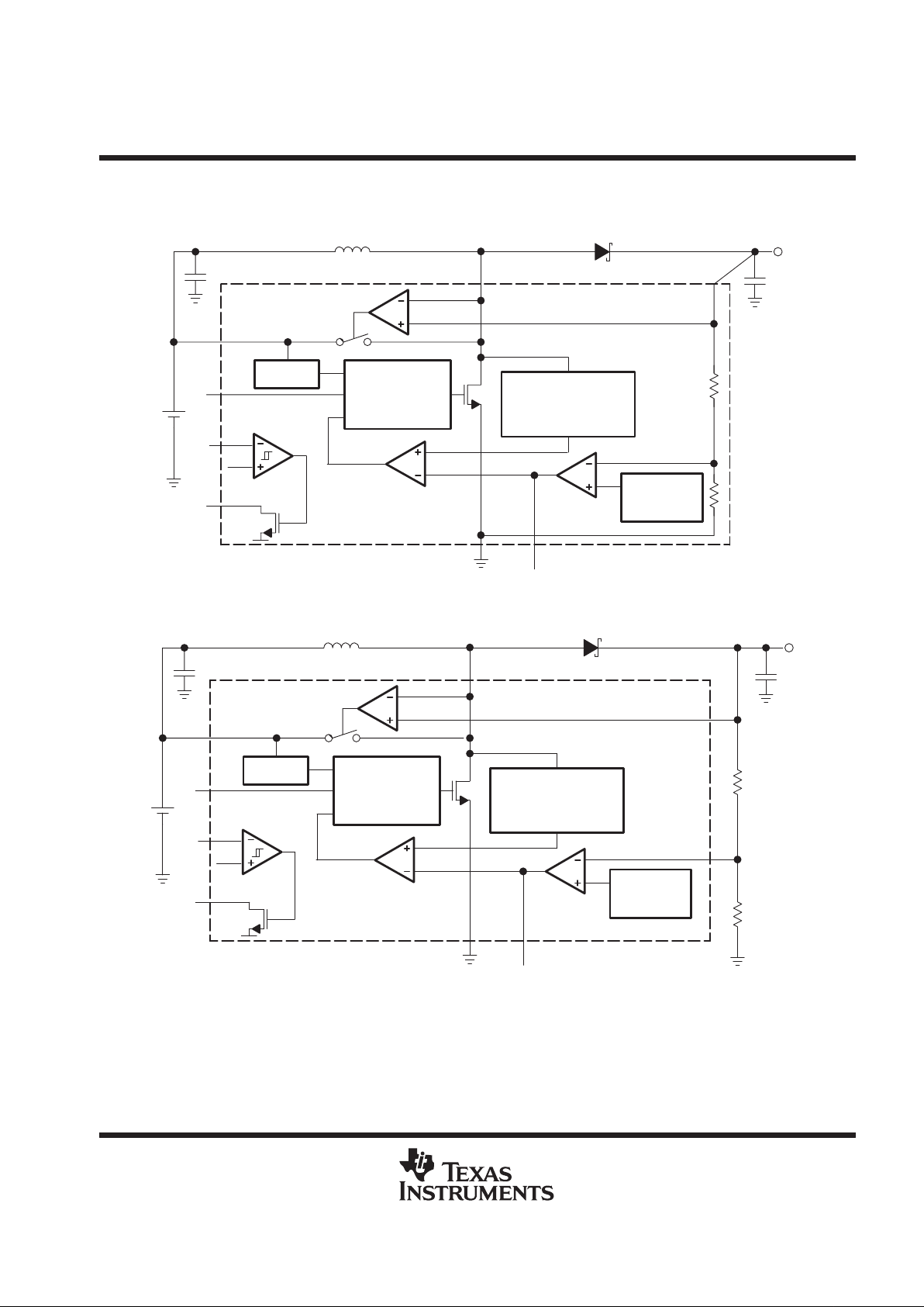
functional block diagram
fixed output-voltage option
V
REF
V
BAT
Control Logic
Oscillator
Gate Drive
UVLO
Current Sense
Current Limit
Slope Compensation
Bandgap
Reference
EN
LBI
LBO
GND COMP
L1 D1
V
OUT
C
O
C
I
SW
Comparator
LBI/LBO
Comparator
Error
Amplifier
Anti-Ringing
Comparator
and Switch
adjustable output-voltage option
V
REF
V
BAT
Control Logic
Oscillator
Gate Drive
UVLO
Current Sense
Current Limit
Slope Compensation
Bandgap
Reference
EN
LBI
LBO
GND COMP
L1 D1
V
OUT
C
O
C
I
SW
Comparator
LBI/LBO
Comparator
Error
Amplifier
Anti-Ringing
Comparator
and Switch
FB

TPS61000, TPS61001, TPS61002, TPS61003, TPS61004, TPS61005, TPS61006
SINGLE-CELL BOOST CONVERTER WITH START-UP INTO FULL LOAD
SLVS279A – MARCH 2000 – REVISED MAY 2000
4
POST OFFICE BOX 655303 • DALLAS, TEXAS 75265
detailed description
controller circuit
The device is based on a current-mode control topology using a constant-frequency pulse-width modulator to
regulate the output voltage. It runs at an oscillator frequency of 500 kHz. The current sense is implemented by
measuring the voltage across the switch. The controller also limits the current through the power switch on a
pulse by pulse basis. Care must be taken that the inductor saturation current is higher than the current limit of
the TPS6100x. This prevents the inductor from going into saturation and therefore protects both device and
inductor. The current limit should not become active during normal operating conditions.
The TPS6100x is designed for high efficiency over a wide output current range. Even at light loads the efficiency
stays high because the controller enters a power-save
mode, minimizing switching losses of the converter. In
this mode, the controller only switches if the output voltage trips below a set threshold voltage. It ramps up the
output voltage with one or several pulses, and again goes into the power-save mode once the output voltage
exceeds the threshold voltage. The controller enters the power-save mode when the output current drops to
levels that force the discontinuous current mode. It calculates a minimum duty cycle based on input and output
voltage and uses the calculation for the transition out of the
power-save mode into continuous current mode.
The control loop must be externally compensated with an R/C/C network connected to the COMP pin. See the
application section for more details on the design of the compensation network.
device enable
The device is put into operation when EN is set high. During start-up of the converter the input current from the
battery is limited until the voltage on COMP reaches its operating point. The device is put into a shutdown mode
when EN is set to GND. In this mode, the regulator stops switching and all internal control circuitry including
the low-battery comparator is switched off. The output voltage drops to one diode drop below the input voltage
in shutdown.
under-voltage lockout
An under-voltage lockout function prevents the device start-up if the supply voltage on V
BAT
is lower than
approximately 0.7 V . This under-voltage lockout function is implemented in order to prevent the malfunctioning
of the converter. When in operation and the battery is being discharged, the device will automatically enter the
shutdown mode if the voltage on V
BAT
drops below approximately 0.7 V.
If the EN pin is hardwired to V
BAT
and if the voltage at V
BAT
drops temporarily below the UVLO threshold voltage,
the device will switch off and will not start up again automatically , even if the supply voltage rises above 0.9 V.
The device will start up again only after a signal change from low to high on EN or if the battery voltage is
completely removed.

TPS61000, TPS61001, TPS61002, TPS61003, TPS61004, TPS61005, TPS61006
SINGLE-CELL BOOST CONVERTER WITH START-UP INTO FULL LOAD
SLVS279A – MARCH 2000 – REVISED MAY 2000
5
POST OFFICE BOX 655303 • DALLAS, TEXAS 75265
detailed description (continued)
low Battery detector circuit (LBI and LBO)
The low-battery detector circuit is typically used to supervise the battery voltage and to generate an error flag
when the battery voltage drops below a user-set threshold voltage. The function is active only when the device
is enabled. When the device is disabled, the LBO pin is high impedance. The LBO pin goes active low when
the voltage on the LBI pin decreases below the set threshold voltage of 500 mV ±15 mV , which is equal to the
internal reference voltage. The battery voltage, at which the detection circuit switches, can be programmed with
a resistive divider connected to the LBI pin. The resistive divider scales down the battery voltage to a voltage
level of 500 mV, which is then compared to the LBI threshold voltage. The LBI pin has a build-in hysteresis of
10 mV. Please see the application section for more details about the programming of the LBI threshold.
If the low-battery detection circuit is not used, the LBI pin should be connected to GND (or to V
BAT
) and the LBO
pin can be left unconnected. Do not let the LBI pin float.
low-EMI switch
The device integrates a circuit which removes the ringing that typically appears on the SW-node when the converter enters the discontinuous current mode. In this case, the current through the inductor ramps to zero and
the Schottky diode stops conducting. Due to remaining energy that is stored in parasitic components of diode,
inductor and switch, a ringing on the SW pin is induced. The integrated anti-ringing switch clamps this voltage
internally to V
BAT
and therefore dampens this ringing.
The anti-ringing switch is turned on by a comparator that monitors the voltage between SW and V
OUT
. This
voltage indicates when the diode is reverse biased. The ringing on the SW-node is damped to a large degree,
reducing the electromagnetic interference generated by the switching regulator to a very great extends.
adjustable output voltage
The accuracy of the internal voltage reference, the controller topology , and the accuracy of the external resistor
divider determine the accuracy of the adjustable output voltage version of the TPS61000. The reference voltage
has an accuracy of ±4% over line, load, and temperature. The controller switches between fixed frequency and
pulse-skip mode, depending on load current. This adds an offset to the output voltage that is equivalent to 1%
of VO. Using 1% accurate resistors for the feedback divider, a total accuracy of ±6% can be achieved over the
complete output current range.
TPS61000, TPS61001, TPS61002, TPS61003, TPS61004, TPS61005, TPS61006
SINGLE-CELL BOOST CONVERTER WITH START-UP INTO FULL LOAD
SLVS279A – MARCH 2000 – REVISED MAY 2000
6
POST OFFICE BOX 655303 • DALLAS, TEXAS 75265
absolute maximum ratings
†
Input voltage range, VI (V
BAT
, V
OUT
, COMP, FB, LBO, EN, LBI) –0.3 V to 3.6 V. . . . . . . . . . . . . . . . . . . . . . . . .
Input voltage, VI (SW) –0.3 V to 7 V. . . . . . . . . . . . . . . . . . . . . . . . . . . . . . . . . . . . . . . . . . . . . . . . . . . . . . . . . . . . . .
Peak current into SW 1300 mA. . . . . . . . . . . . . . . . . . . . . . . . . . . . . . . . . . . . . . . . . . . . . . . . . . . . . . . . . . . . . . . . . . .
Continuous total power dissipation See dissipation rating table. . . . . . . . . . . . . . . . . . . . . . . . . . . . . . . . . . . . . . . .
Operating free-air temperature range, T
A
–40°C to 85°C. . . . . . . . . . . . . . . . . . . . . . . . . . . . . . . . . . . . . . . . . . . . .
Maximum junction temperature, T
J
150°C. . . . . . . . . . . . . . . . . . . . . . . . . . . . . . . . . . . . . . . . . . . . . . . . . . . . . . . . .
Storage temperature range, T
stg
–65°C to 150°C. . . . . . . . . . . . . . . . . . . . . . . . . . . . . . . . . . . . . . . . . . . . . . . . . . . .
Lead temperature 260°C. . . . . . . . . . . . . . . . . . . . . . . . . . . . . . . . . . . . . . . . . . . . . . . . . . . . . . . . . . . . . . . . . . . . . . . .
†
Stresses beyond those listed under “absolute maximum ratings” may cause permanent damage to the device. These are stress ratings only, and
functional operation of the device at these or any other conditions beyond those indicated under “recommended operating conditions” is not
implied. Exposure to absolute-maximum-rated conditions for extended periods may affect device reliability.
DISSIPATION RATING TABLE
PACKAGE
TA ≤ 25_C
POWER RATING
DERATING FACTOR
ABOVE TA = 25_C
TA = 70_C
POWER RATING
TA = 85_C
POWER RATING
DGS 424 mW 3.4 mW/_C 271 mW 220 mW
recommended operating conditions
MIN NOM MAX UNIT
Supply voltage at V
BAT
0.8 V
O
V
p
V
BAT
= 1.2 V 100
Output current
V
BAT
= 2.4 V 250
mA
Inductor 10 33 µH
Input capacitor 10 µF
Output capacitor 22 µF
Operating junction temperature, T
J
–40 125 °C
TPS61000, TPS61001, TPS61002, TPS61003, TPS61004, TPS61005, TPS61006
SINGLE-CELL BOOST CONVERTER WITH START-UP INTO FULL LOAD
SLVS279A – MARCH 2000 – REVISED MAY 2000
7
POST OFFICE BOX 655303 • DALLAS, TEXAS 75265
electrical characteristics over recommended operating free-air temperature range, V
BA T
= 1.2 V , EN
= V
BAT
(unless otherwise noted)
PARAMETER TEST CONDITIONS MIN TYP MAX UNIT
V
I
Input voltage for start-up RL = 33 Ω 0.9 V
V
I
Input voltage for start-up RL = 3 kΩ, TA = 25 °C 0.8 V
V
I
Input voltage once started IO = 100 mA 0.8 V
V
O
Programmable output voltage range TPS61000 IO = 100 mA 1.5 3.3 V
1.2 V IO = 1 mA 1.44 1.5 1.55
TPS61001
0.8 V < VI < VO, IO = 100 mA 1.45 1.5 1.55
1.2 V IO = 1 mA 1.72 1.8 1.86
TPS61002
0.8 V < VI < VO, IO = 100 mA 1.74 1.8 1.86
1.2 V IO = 1 mA 2.40 2.5 2.58
TPS61003
0.8 V < VI < VO, IO = 100 mA 2.42 2.5 2.58
1.6 V < VI < VO, IO = 200 mA 2.42 2.5 2.58
p
1.2 V IO = 1 mA 2.68 2.8 2.89
VOOutput voltage
TPS61004
0.8 V < VI < VO, IO = 100 mA 2.72 2.8 2.89
V
1.6 V < VI < VO, IO = 200 mA 2.72 2.8 2.89
1.2 V IO = 1 mA 2.88 3.0 3.1
TPS61005
0.8 V < VI < VO, IO = 100 mA 2.9 3.0 3.1
1.6 V < VI < VO, IO = 200 mA 2.9 3.0 3.1
1.2 V IO = 1 mA 3.16 3.3 3.4
TPS61006
0.8 V < VI < VO, IO = 100 mA 3.2 3.3 3.4
1.6 V < VI < VO, IO = 200 mA 3.2 3.3 3.4
p
VI = 0.8 V 100
IOMaximum continuous output current
VI = 1.8 V 250
mA
TPS61001 0.5
TPS61002 0.65
TPS61003
0.9
ISWSwitch current limit
TPS61004
0.8 V
<
V
I
<
V
O
0.95
A
TPS61005 1
TPS61006 1.1
V
FB
Feedback voltage TPS61006 468 500 515 mV
f Oscillator frequency 360 500 840 kHz
D
MAX
Maximum duty cycle 85%
r
DS(on)
Switch-on resistance VO = 3.3 V 0.18 0.27 Ω
Line regulation (see Note 1) VI = 0.8V to 1.25V , IO = 50 mA 0.3 %/V
Load regulation fixed output voltage versions
(see Note 1)
VI = 1.2 V; IO = 10 mA to 90 mA 0.25%
NOTE 1: Line and load regulation is measured as a percentage deviation from the nominal value (i.e. as percentage deviation from the nominal
output voltage). For line regulation, x %/V stands for ±x% change of the nominal output voltage per 1-V change on the input/supply
voltage. For load regulation, y% stands for ±y% change of the nominal output voltage per the specified current change.

TPS61000, TPS61001, TPS61002, TPS61003, TPS61004, TPS61005, TPS61006
SINGLE-CELL BOOST CONVERTER WITH START-UP INTO FULL LOAD
SLVS279A – MARCH 2000 – REVISED MAY 2000
8
POST OFFICE BOX 655303 • DALLAS, TEXAS 75265
electrical characteristics over recommended operating free-air temperature range, V
BA T
= 1.2 V , EN
= V
BAT
(unless otherwise noted) (continued)
PARAMETER TEST CONDITIONS MIN TYP MAX UNIT
Quiescent current drawn from power source IO = 0 mA
V
BAT
44
I
Q
(current into V
BAT
and into V
OUT
)
O
VEN = VI, VO = 3.4 V
V
OUT
6
µ
A
I
SD
Shutdown current from power source
(current into V
BAT
and into V
OUT
)
VEN = 0 V 0.2 5 µA
V
IL
EN low-level input voltage
0.2 ×
V
BAT
V
V
IH
EN high-level input voltage
0.8 ×
V
BAT
V
EN input current EN = GND or V
BAT
0.1 1 µA
V
IL
LBI low-level input voltage threshold V
LBI
voltage decreasing 470 500 530 mV
LBI input hysteresis 10 mV
I
I
LBI input current 0.01 0.1 µA
V
OL
LBO low-level output voltage V
LBI
= 0 V, VO = 3.3 V, IOL = 50 µA 0.04 0.2 V
LBO output leakage current V
LBI
= 650 mV , V
LBO
= 3.3 V 0.01 1 µA
I
FB
FB input bias current (TPS61000 only) VFB = 500 mV 0.01 0.1 µA
PARAMETER MEASUREMENT INFORMATION
List of Components:
IC1: Only fixed output versions
(unless otherwise noted)
L1: Coilcraft DO3308P–333
D1: Motorola Schottky Diode
MBRM120L T3
CI: Ceramic
CO:
Ceramic
5
6
TPS6100x
9
8
1
10
3
2
7
4
SW
V
BAT
LBI
NC
EN
V
OUT
LBO
FB
COMP
GND
Low Battery
Warning
R4
10 kΩ
R3
ON
OFF
R2
R1
C
i
10 µF
L1
D1
C1
100 pF
C2
33 nF
C
o
22 µF
33 µH
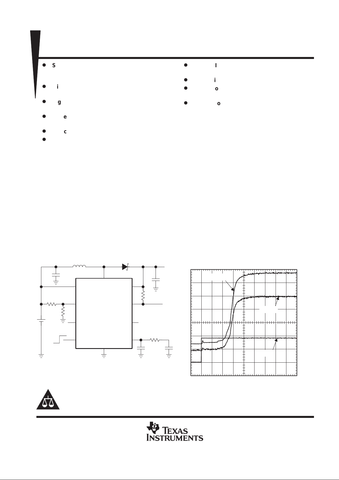
Figure 1. Circuit Used For Typical Characteristics Measurements

TPS61000, TPS61001, TPS61002, TPS61003, TPS61004, TPS61005, TPS61006
SINGLE-CELL BOOST CONVERTER WITH START-UP INTO FULL LOAD
SLVS279A – MARCH 2000 – REVISED MAY 2000
9
POST OFFICE BOX 655303 • DALLAS, TEXAS 75265
TYPICAL CHARACTERISTICS
Table of Graphs
FIGURE
vs Output Current 2, 3
η Efficiency
vs Inductor Type 4
vs Input Voltage 5
I
O
Maximum Output Current vs Input Voltage 6
V
O
Output Voltage vs Output Current 7
V
O
TPS61000 Output Voltage vs Output Current 8
I
Q
No-Load Supply Current vs Input Voltage 9
I
SD
Shutdown Current vs Input Voltage 10
V
I
Minimum Start-Up Input Voltage vs Load Current 11
I
LIM
Switch current limit vs Output Voltage 12
Output Voltage Ripple Amplitude 13
Output Voltage Ripple Amplitude 14
Load Transient Response 15
Line Transient Response 16
Start-Up Timing 17
Figure 2
50
40
20
0
110
Efficiency – %
80
90
EFFICIENCY
vs
OUTPUT CURRENT
100
100
70
60
30
10
VO = 3.3 V
VO = 1.5 V
VI = 1.2 V
IO – Output Current – mA
1000
Figure 3
0
10
20
30
40
50
60
70
80
90
100
1 10 100 1000
VO = 3.3 V
VO = 2.8 V
VI = 2.4 V
Efficiency – %
EFFICIENCY
vs
OUTPUT CURRENT
IO – Output Current – mA

TPS61000, TPS61001, TPS61002, TPS61003, TPS61004, TPS61005, TPS61006
SINGLE-CELL BOOST CONVERTER WITH START-UP INTO FULL LOAD
SLVS279A – MARCH 2000 – REVISED MAY 2000
10
POST OFFICE BOX 655303 • DALLAS, TEXAS 75265
TYPICAL CHARACTERISTICS
50
55
60
65
70
75
80
85
90
95
100
Coilcraft
DO1608C
Coilcraft
DS1608C
Coiltronics
UP1B
Coiltronics
UP2B
Sumida
CD43
Sumida
CD54
Efficiency – %
EFFICIENCY
vs
INDUCTOR TYPE
Inductor Type
VI = 1.2 V
VO = 3.3 V
IO = 100 mA
Figure 4
60
65
70
75
80
85
90
95
0.80 1.30 1.80 2.30 2.80 3.30
Efficiency – %
EFFICIENCY
vs
INPUT VOLTAGE
VI – Input Voltage – V
IO = 50 mA
IO = 100 mA
Figure 5
0
0.10
0.20
0.30
0.40
0.50
0.60
0.70
0.80
0.90
1
0.8 1 1.2 1.4 1.6 1.8 2 2.2 2.4 2.6 2.8 3
– Output Current –
MAXIMUM OUTPUT CURRENT
vs
INPUT VOLTAGE
A
VI – Input Voltage – V
VO = 1.45 V
VO = 1.75 V
Figure 6
I
O
VO = 2.42 V
VO = 3.2 V

TPS61000, TPS61001, TPS61002, TPS61003, TPS61004, TPS61005, TPS61006
SINGLE-CELL BOOST CONVERTER WITH START-UP INTO FULL LOAD
SLVS279A – MARCH 2000 – REVISED MAY 2000
11
POST OFFICE BOX 655303 • DALLAS, TEXAS 75265
TYPICAL CHARACTERISTICS
1.60
1.80
2.00
2
2.40
2.60
2.80
3
3.20
3.40
3.60
1 10 100 1000
VI = 1.2 V
3.3 V
2.5 V
1.8 V
– Output Voltage – V
TPS61002/3/6
OUTPUT VOLTAGE
vs
OUTPUT CURRENT
V
O
IO – Output Current – mA
Figure 7
Figure 8
1.60
1.80
2
2.20
2.40
2.60
2.80
3
3.20
3.40
3.60
0.1 1 10 100 1000
VO = 3.3 V
– Output Voltage – V
TPS61000
OUTPUT VOLTAGE
vs
OUTPUT CURRENT
V
O
IO – Output Current – mA
VO = 2.5 V
VO = 1.8 V
Figure 9
0
5
10
15
20
25
30
35
40
45
0.80 1.30 1.80 2.30 2.80 3.30 3.80
TA = 85°C
TA = 25°C
TA = –40°C
– Supply Current –
NO-LOAD SUPPLY CURRENT
vs
INPUT VOLTAGE
Aµ
VI – Input Voltage – V
I
Q
Figure 10
0
200
400
600
800
1000
1200
1400
1600
1800
0.80 1.30 1.80 2.30 2.80 3.30 3.80
Supply Current – nA
SHUTDOWN CURRENT
vs
INPUT VOLTAGE
VI – Input Voltage – V
TA = 85°C
TA = 25°C
TA = –40°C

TPS61000, TPS61001, TPS61002, TPS61003, TPS61004, TPS61005, TPS61006
SINGLE-CELL BOOST CONVERTER WITH START-UP INTO FULL LOAD
SLVS279A – MARCH 2000 – REVISED MAY 2000
12
POST OFFICE BOX 655303 • DALLAS, TEXAS 75265
TYPICAL CHARACTERISTICS
Figure 11
0.60
0.65
0.70
0.75
0.80
0.85
0.90
010
20
100
VO = min 3.2 V
– Input Voltage – V
MINIMUM START-UP INPUT VOLTAGE
vs
LOAD CURRENT
V
I
IO – Output Current – mA
30 40 50 60 70 80 90
Figure 12
0
0.5
1
1.5
1.5 1.7 1.9 2.1 2.3 2.5 2.7 2.9 3.1 3.3 3.5
VI = 1.2 V
Switch Current Limit – A
TPS61000
SWITCH CURRENT LIMIT
vs
OUTPUT VOLTAGE
VO – Output Voltage – V
Figure 13
3.28
3.26
3.22
3.18
3.30
3.32
TPS61006
OUTPUT VOLTAGE RIPPLE AMPLITUDE
3.34
3.24
3.20
IO = 2 mA
time – ms
– Output Voltage – VV
O
01 5432
Figure 14
3.30
0123
3.32
3.34
3.36
45
TPS61006
OUTPUT VOLTAGE RIPPLE AMPLITUDE
2
0
time – µs
VI = 1.2 V
– Output Voltage – V
V
SW
V
OUT
V
O
V
SW

TPS61000, TPS61001, TPS61002, TPS61003, TPS61004, TPS61005, TPS61006
SINGLE-CELL BOOST CONVERTER WITH START-UP INTO FULL LOAD
SLVS279A – MARCH 2000 – REVISED MAY 2000
13
POST OFFICE BOX 655303 • DALLAS, TEXAS 75265
TYPICAL CHARACTERISTICS
Figure 15
3.2
20
0
0123456
3.3
3.4
TPS61006
LOAD TRANSIENT RESPONSE
78910
60
40
– Output Voltage – V
V
O
VI = 1.2 V
RC = 33 kΩ
50 mA
5 mA
– Output Current – mA
I
O
time – ms
Figure 16
3.25
1.2
1
0123456
3.35
3.45
TPS61006
LINE TRANSIENT RESPONSE
3.55
78910
0.8
– Output Voltage – V
V
O
– Input Voltage – V
V
I
V
OUT
V
BAT
time – ms
IO = 50 mA
RC = 33 kΩ
2
024681012
3
TPS61006
START-UP TIMING INTO 33 Ω LOAD
14 16 18 20
1
0
– Output Voltage – V
V
O
V
OUT
EN
I
OUT
80
60
20
100
120
140
0
40
– Output Current – mA
I
O
time – ms
Figure 17

TPS61000, TPS61001, TPS61002, TPS61003, TPS61004, TPS61005, TPS61006
SINGLE-CELL BOOST CONVERTER WITH START-UP INTO FULL LOAD
SLVS279A – MARCH 2000 – REVISED MAY 2000
14
POST OFFICE BOX 655303 • DALLAS, TEXAS 75265
APPLICATION INFORMATION
The TPS6100x boost converter family is intended for systems that are powered by a single-cell NiCd or NiMH
battery with a typical terminal voltage between 0.9 V to 1.6 V . It can also be used in systems that are powered
by two-cell NiCd or NiMH batteries with a typical stack voltage between 1.8 V and 3.2 V. Additionally, singleor dual-cell, primary and secondary alkaline battery cells can be the power source in systems where the
TPS6100x is used.
programming the TPS61000 adjustable output voltage device
The output voltage of the TPS61000 can be adjusted with an external resistor divider. The typical value of the
voltage on the FB pin is 500 mV in fixed frequency operation and 485 mV in the power-save operation mode.
The maximum allowed value for the output voltage is 3.3 V . The current through the resistive divider should be
about 100 times greater than the current into the FB pin. The typical current into the FB pin is 0.01 µA, the voltage
across R4 is typically 500 mV. Based on those two values, the recommended value for R4 is in the range of
500 kΩ in order to set the divider current at 1 µA. From that, the value of resistor R3, depending on the needed
output voltage V
OUT
, can be calculated using the following equation:
R3+R4
ǒ
V
O
V
FB
*
1
Ǔ +
500 kΩ
ǒ
V
O
500 mV
*
1
Ǔ
(1)
If, as an example, an output voltage of 2.5 V is needed, a 2 MΩ resistor should be chosen for R3.
V
BAT
V
OUT
LBO
5
10
3
R5 R3
R4
6
TPS61000
LBI
9
FB
COMP
2
C
C1
100 pF
C
C2
33 nF
R
C
10 kΩ
EN
NC
R2
R1
1
8
GND
SW
7
4
C
i
10 µF
10 V
C
o
22 µF
10 V
Low Battery
Warning
L1
33 µH
D1
Figure 18. Typical Application Circuit for Adjustable Output Voltage Option
The output voltage of the adjustable output voltage version changes with the output current. Due to
device-internal ground shift, which is caused by the high switch current, the internal reference voltage and hence
the voltage on the FB pin increases with increasing output current. Since the output voltage follows the voltage
on the FB pin, the output voltage rises as well with a rate of 1 mV per 1 mA output current increase. Additionally ,
when the converter goes into pulse-skip mode at output currents around 5 mA and lower, the output voltage
drops due to the hysteresis of the controller. This hysteresis is about 15 mV measured on the FB pin.

TPS61000, TPS61001, TPS61002, TPS61003, TPS61004, TPS61005, TPS61006
SINGLE-CELL BOOST CONVERTER WITH START-UP INTO FULL LOAD
SLVS279A – MARCH 2000 – REVISED MAY 2000
15
POST OFFICE BOX 655303 • DALLAS, TEXAS 75265
APPLICATION INFORMATION
programming the low battery comparator threshold voltage
The current through the resistive divider should be about 100 times greater than the current into the LBI pin.
The typical current into the LBI pin is 0.01 µA, the voltage across R2 is equal to the reference voltage that is
generated on chip, which has a value of 500 mV ±15 mV. The recommended value for R2 is therefore in the
range of 500 kΩ. From that, the value of resistor R1 depending on the desired minimum battery voltage V
BAT
,
can be calculated using below equation:
R1+R2
ǒ
V
TRIP
V
REF
*
1Ǔ+
500 kΩ
ǒ
V
BAT
0.5 V
*
1
Ǔ
(2)
For example, if the low-battery detection circuit should flag an error condition on the LBO output pin at a battery
voltage of 1.0 V, a resistor in the range of 500 kΩ should be chosen for R1.
The output of the low battery comparator is a simple open-drain output that goes active low if the battery voltage
drops below the programmed threshold voltage on LBI. The output requires a pullup resistor with a
recommended value of 1MΩ, and should only be pulled up to the V
OUT
. If not used, the LBO pin can be left
floating.
inductor selection
The output filter of inductive switching regulators is a low pass filter of second order. It consists of an inductor and
a capacitor, often referred to as storage inductor and output capacitor.
To select an inductor, keep the possible peak inductor current below the current limit threshold of the power
switch in your chosen configuration. For example, the current limit threshold of the TPS61000’s switch is
1 100 mA at an output voltage of 3.3 V . The highest peak current through the inductor and the switch depends on
the output load, the input (V
BAT
) and the output voltage (V
OUT
). Estimation of the maximum average inductor
current can be done using the following equation:
IL+
I
OUT
x
V
OUT
V
BAT
x0.8
(3)
For example, for an output current of 100 mA at 3.3 V , at least 515 mA current will flow through the inductor at a
minimum input voltage of 0.8 V.
The second parameter for choosing the inductor is the desired current ripple in the inductor. Normally it is advisable to work with a ripple of less than 20% of the average inductor current. A smaller ripple will reduce the magnetic hysteresis losses in the inductor as well as output voltage ripple and EMI. But in the same way , regulation
time at load changes will rise. In addition, a larger inductor will increase the total system costs.

TPS61000, TPS61001, TPS61002, TPS61003, TPS61004, TPS61005, TPS61006
SINGLE-CELL BOOST CONVERTER WITH START-UP INTO FULL LOAD
SLVS279A – MARCH 2000 – REVISED MAY 2000
16
POST OFFICE BOX 655303 • DALLAS, TEXAS 75265
APPLICATION INFORMATION
With those parameters it is possible to calculate the value for the inductor:
L
+
V
BAT
xǒV
OUT
–V
BAT
Ǔ
∆ILxfxV
OUT
(4)
Parameter f is the switching frequency and ∆IL is the ripple current in the inductor, i.e. 20% x IL.
In this example, the desired inductor will have the value of 12 µH. With this calculated value and the calculated
currents, it is possible to chose a suitable inductor. Care has to be taken that load transients and losses in the
circuit can lead to higher currents as estimated in equation 3. Also, the losses in the inductor caused by magnetic
hysteresis losses and copper losses are a major parameter for total circuit efficiency.
The following inductors from different suppliers were tested. All will work with the TPS6100x converter within
their specified parameters:
Table 1. Recommended Inductors
VENDOR PART NUMBER
Coilcraft DO1608P Series
DS1608P Series
DO3308 Series
Coiltronics UP1B Series
UP2B Series
Murata LQH3N Series
Sumida CD43 Series
CD54 Series
CDR74B Series
TDK NLC453232T Series
capacitor selection
The major parameter necessary to define the output capacitor is the maximum allowed output voltage ripple of
the converter. This ripple is determined by two parameters of the capacitor, the capacitance and the ESR. It is
possible to calculate the minimum capacitance needed for the defined ripple, supposing that the ESR is zero.
C
min
+
I
OUT
xǒV
OUT
–V
BAT
Ǔ
fx∆VxV
OUT
(5)
Parameter f is the switching frequency and ∆V is the maximum allowed ripple.
With a chosen ripple voltage of 15 mV , a minimum capacitance of 10 µF is needed. The total ripple will be larger
due to the ESR of the output capacitor. This additional component of the ripple can be calculated using the following equation:
∆V
ESR
+
I
OUT
xR
ESR
(6)

TPS61000, TPS61001, TPS61002, TPS61003, TPS61004, TPS61005, TPS61006
SINGLE-CELL BOOST CONVERTER WITH START-UP INTO FULL LOAD
SLVS279A – MARCH 2000 – REVISED MAY 2000
17
POST OFFICE BOX 655303 • DALLAS, TEXAS 75265
APPLICATION INFORMATION
An additional ripple of 30 mV is the result of using a tantalum capacitor with a low ESR of 300 mΩ. The total ripple
is the sum of the ripple caused by the capacitance and the ripple caused by the ESR of the capacitor. In this
example, the total ripple will be 45 mV. It is possible to improve the design by enlarging the capacitor or using
smaller capacitors in parallel to reduce the ESR or by using better capacitors with lower ESR, like ceramics. For
example, a 10 µF ceramic capacitor with an ESR of 50 mΩ is used on the evaluation module (EVM). Tradeoffs
have to be made between performance and costs of the converter circuit.
A 10 µF input capacitor is recommended to improve transient behavior of the regulator. A ceramic capacitor or a
tantalum capacitor with a 100 nF ceramic capacitor in parallel placed close to the IC is recommended.
rectifier selection
The rectifier diode has a major impact on the overall converter efficiency. Standard diodes are not suitable for
low-voltage switched mode power supplies. A Schottky diode with low forward voltage and fast reverse recovery
should be used as rectifier to minimize overall losses of the dc-dc converter. The maximum current rating of the
diode must be high enough for the application. The maximum diode current is equal to the maximum current in
the inductor that was calculated in equation 3. The maximum reverse voltage is the output voltage. The chosen
diode should therefore have a reverse voltage rating higher than the output voltage.
Table 2. Recommended Diodes
VENDOR PART NUMBER
Motorola Surface Mount MBRM120LT3
MBR0520L T1
Motorola Axial Lead 1N1517
ROHM RB520S-30
RB160L–40
The typical forward voltage of those diodes is in the range of 0.35 to 0.45 V assuming a peak diode current of
600 mA.
compensation of the control loop
An R/C/C network must be connected to the COMP pin in order to stabilize the control loop of the converter. Both
the pole generated by the inductor L1 and the zero caused by the ESR and capacitance of the output capacitor
must be compensated. The network shown in Figure 19 will satisfy these requirements.
C
C2
33 nF
C
C1
100 pF
R
C
10 kΩ
COMP
Figure 19. Compensation of the Control Loop

TPS61000, TPS61001, TPS61002, TPS61003, TPS61004, TPS61005, TPS61006
SINGLE-CELL BOOST CONVERTER WITH START-UP INTO FULL LOAD
SLVS279A – MARCH 2000 – REVISED MAY 2000
18
POST OFFICE BOX 655303 • DALLAS, TEXAS 75265
APPLICATION INFORMATION
Resistor RC and capacitor CC2 depend on the chosen inductance. For a 33 µH inductor, the capacitance of C
C2
should be chosen to 33 nF , or in other words, if the inductor is xx µH, the chosen compensation capacitor should
be xx nF , the same number value. The value of the compensation resistor is then chosen based on the requirement to have a time constant of 0.3 ms for the R/C network of RC and CC2; hence for a 33-nF capacitor, a 10-kΩ
resistor should be chosen for RC.
Capacitor CC1 is depending on the ESR and capacitance value of the output capacitor, and on the value chosen
for RC. Its value is calculated using following equation:
CC1+
COx ESR
COUT
3 R
C
(7)
For a selected output capacitor of 22 µF with an ESR of 0.2 Ω, and RC of 33 kΩ, the value of CC1 is in the range of
100 pF.
Table 3. Recommended Compensation Components
OUTPUT CAPACITOR
INDUCTOR
[µH]
CAPACITANCE
[µF]
ESR
[Ω]
R
C
[kΩ]
C
C1
[pF]
C
C2
[nF]
33 22 0.2 10 100 33
22 22 0.3 15 100 22
10 22 0.4 33 100 10
10 10 0.1 33 100 10
schematic of TPS6100x evaluation modules (TPS6100xEVM–156)
LBO
LBI
NC
SW
V
BAT
EN
COMP
FB
GND
V
OUT
R6
LP1
D1
L1
C1 C3
R2 R1
IN
J1
C6
R5
C5
R3
C2
R4
OUT
TPS6100x

TPS61000, TPS61001, TPS61002, TPS61003, TPS61004, TPS61005, TPS61006
SINGLE-CELL BOOST CONVERTER WITH START-UP INTO FULL LOAD
SLVS279A – MARCH 2000 – REVISED MAY 2000
19
POST OFFICE BOX 655303 • DALLAS, TEXAS 75265
APPLICATION INFORMATION
suggested board layout and component placement (21 mm x 21 mm board size)
Figure 20. Top Layer Layout and Component Placement
Figure 21. Bottom Layer Layout and Component Placement
device family products
Other devices in this family are:
PART NUMBER DESCRIPTION
UCC2941-3/-5/-ADJ
p
UCC3941-3/-5/-ADJ
1-V synchronous boost converter with secondary output
UCC29411/2/3
p
p
UCC39411/2/3
1-V low power synchronous boost converter with secondary output

TPS61000, TPS61001, TPS61002, TPS61003, TPS61004, TPS61005, TPS61006
SINGLE-CELL BOOST CONVERTER WITH START-UP INTO FULL LOAD
SLVS279A – MARCH 2000 – REVISED MAY 2000
20
POST OFFICE BOX 655303 • DALLAS, TEXAS 75265
THERMAL INFORMATION
Implementation of integrated circuits in low-profile and fine-pitch surface-mount packages typically requires
special attention to power dissipation. Many system-dependent issues such as thermal coupling, airflow, added
heat sinks and convection surfaces, and the presence of other heat-generating components affect the powerdissipation limits of a given component.
Three basic approaches for enhancing thermal performance are listed below:
• Improving the power dissipation capability of the PWB design
• Improving the thermal coupling of the component to the PWB
• Introducing airflow in the system
The maximum junction temperature (TJ) of the TPS6100x devices is 125°C. The thermal resistance of the
10-pin MSOP package (DSG) is R
θJA
= 294°C/W. Specified regulator operation is assured to a maximum
ambient temperature T
A
of 85 °C. Therefore, the maximum power dissipation is about 130 mW. More power can
be dissipated if the maximum ambient temperature of the application is lower.
mW
WC
CC
JA
R
A
MAXJ
T
MAXD
P 136
/294
85125)(
)(
=
°
°–°
=
Θ
=
(8)
–
Under normal operating conditions, the sum of all losses generated inside the converter IC is less than 50 mW,
which is well below the maximum allowed power dissipation of 136 mW as calculated in equation 8. Therefore,
power dissipation is given no special attention.
Table 4 shows where the losses inside the converter are generated.
Table 4. Losses Inside the Converter
LOSSES AMOUNTS
Conduction losses in the switch 36 mW
Switching losses 8 mW
Gate drive losses 2.3 mW
Quiescent current losses < 1 mW
TOTAL < 50 mW

TPS61000, TPS61001, TPS61002, TPS61003, TPS61004, TPS61005, TPS61006
SINGLE-CELL BOOST CONVERTER WITH START-UP INTO FULL LOAD
SLVS279A – MARCH 2000 – REVISED MAY 2000
21
POST OFFICE BOX 655303 • DALLAS, TEXAS 75265
MECHANICAL DATA
DGS (S-PDSO-G10) PLASTIC SMALL-OUTLINE PACKAGE
0,69
0,41
0,25
0,15 NOM
Gage Plane
4073272/A 03/98
4,98
0,17
6
3,05
4,78
2,95
10
5
3,05
2,95
1
0,27
0,15
0,05
1,07 MAX
Seating Plane
0,10
0,50
M
0,25
0°–6°
NOTES: A. All linear dimensions are in millimeters.
B. This drawing is subject to change without notice.
C. Body dimensions do not include mold flash or protrusion.

IMPORTANT NOTICE
T exas Instruments and its subsidiaries (TI) reserve the right to make changes to their products or to discontinue
any product or service without notice, and advise customers to obtain the latest version of relevant information
to verify, before placing orders, that information being relied on is current and complete. All products are sold
subject to the terms and conditions of sale supplied at the time of order acknowledgment, including those
pertaining to warranty, patent infringement, and limitation of liability.
TI warrants performance of its semiconductor products to the specifications applicable at the time of sale in
accordance with TI’s standard warranty. Testing and other quality control techniques are utilized to the extent
TI deems necessary to support this warranty. Specific testing of all parameters of each device is not necessarily
performed, except those mandated by government requirements.
Customers are responsible for their applications using TI components.
In order to minimize risks associated with the customer’s applications, adequate design and operating
safeguards must be provided by the customer to minimize inherent or procedural hazards.
TI assumes no liability for applications assistance or customer product design. TI does not warrant or represent
that any license, either express or implied, is granted under any patent right, copyright, mask work right, or other
intellectual property right of TI covering or relating to any combination, machine, or process in which such
semiconductor products or services might be or are used. TI’s publication of information regarding any third
party’s products or services does not constitute TI’s approval, warranty or endorsement thereof.
Copyright 2000, Texas Instruments Incorporated
 Loading...