

www.ti.com
95
90
85
80
75
70
65
60
55
50
3 3.5
4 4.5 5 5.5
6
V -InputVoltage-V
I
Efficiency-%
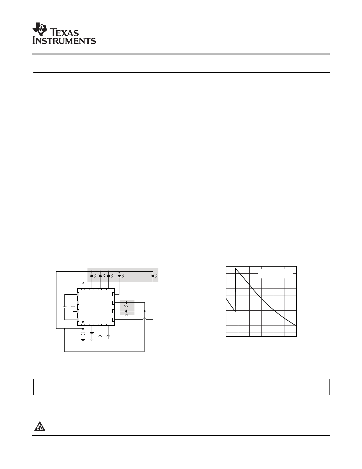
4MainLED-15mA,
V =3.1V
F
C1-
C2+
C2-
C1+
DM1
DM5
DS2
DS1
DM3DM4 DM2
GND
SDAT
SCLKVIN
C1
1mF
C2
1mFC31mF
MainDisplay
C4
4.7mF
SubDisplay
I2CInterface
On/Off, DigitalDimming
VOUT
HIGH EFFICIENCY CHARGE PUMP FOR 7 WLEDs WITH I2C INTERFACE
FEATURES DESCRIPTION
• 3.0-V to 6.0-V Input Voltage Range
• × 1 and × 1.5 Charge Pump
• Fully Programmable Current with I2C
– 64 Dimming Steps with 25mA Maximum
(Sub and Main Display Banks)
– 4 Dimming Steps with 80mA Maximum
(DM5 for Auxiliary Application)
• 2% Current Matching for Sub LEDs at Light
Load Condition (Each 100 µ A)
• 750-kHz Charge Pump Frequency
• Continuous 230-mA Maximum Output Current
• Auto Switching Between × 1 and × 1.5 Mode for
Maximum Efficiency
• Built-in Soft Start and Current Limit
• Open Lamp Detection
• 16-Pin 3mm x 3mm QFN
APPLICATIONS
• Cellular Phones
• PDA, PMP, GPS (Up To 4 Inch LCD Display)
• Multidisplay Handheld Devices
TPS60250
SLVS769 – APRIL 2007
The TPS60250 is a high efficiency, constant
frequency charge pump DC/DC converter that uses a
dual mode 1 × and 1.5 × conversion to maximize
efficiency over the input voltage range. It drives up to
five white LEDs for a main display and up to two
white LEDs for a sub display with regulated constant
current for uniform intensity. By utilizing adaptive
1 × /1.5 × charge pump modes and very low-dropout
current regulators, the TPS60250 achieves high
efficiency over the full 1-cell lithium-battery input
voltage range.
Four enable inputs, ENmain, ENsub1, ENsub2, and
ENaux, available through I2C, are used for simple
on/off controls for the independent main, sub1, sub2,
and DM5 displays, respectively. To lower operating
current when using one sub display LED, the device
provides completely separate operation in sub
display LEDs.
The TPS60250 is available in a 16-pin 3mmx3mm
thin QFN.
Figure 1. Typical Application for Sub and Main Figure 2. Efficiency vs Input Voltage
ORDERING INFORMATION
(1) For the most current package and ordering information, see the Package Option Addendum at the end of this document, or see the TI
PRODUCTION DATA information is current as of publication date.
Products conform to specifications per the terms of the Texas
Instruments standard warranty. Production processing does not
necessarily include testing of all parameters.
PART NUMBER PACKAGE T
TPS60250RTE 16 Pin 3 mm × 3 mm QFN (RTE) –40 ° C to +85 ° C
web site at www.ti.com.
Please be aware that an important notice concerning availability, standard warranty, and use in critical applications of Texas
Instruments semiconductor products and disclaimers thereto appears at the end of this data sheet.
(1)
A
Copyright © 2007, Texas Instruments Incorporated
www.ti.com
TPS60250
SLVS769 – APRIL 2007
These devices have limited built-in ESD protection. The leads should be shorted together or the device placed in conductive foam
during storage or handling to prevent electrostatic damage to the MOS gates.
ABSOLUTE MAXIMUM RATINGS
over operating free-air temperature range (unless otherwise noted)
V
T
T
T
(1) Stresses beyond those listed under absolute maximum ratings may cause permanent damage to the device. These are stress ratings
(2) The Human body model (HBM) is a 100-pF capacitor discharged through a 1.5-k Ω resistor into each pin. The testing is done according
(3) Charged Device Model
(4) Machine Model (MM) is a 200-pF capacitor discharged through a 500-nH inductor with no series resistor into each pin. The testing is
Input voltage range (all pins) –0.3 to 7 V
I
MAX Output current limit 650 mA
HBM ESD Rating
CDM ESD Rating
MM ESD Rating
Operating temperature range –40 to 85 ° C
A
Maximum operating junction temperature 150 ° C
J
Storage temperature –55 to 150 ° C
ST
(2)
(3)
(4)
only and functional operation of the device at these or any other conditions beyond those indicated under recommended operating
conditions is not implied. Exposure to absolute-maximum-rated conditions for extended periods may affect device reliability.
JEDECs EIA/JESD22-A114.
done according JEDECs EIA/JESD22-A115.
(1)
VALUE UNIT
2 kV
500 V
200 V
DISSIPATION RATINGS
PACKAGE
QFN 3 × 3 RTE 74.6 ° C/W 48.7 ° C/W 2.05 W 1.13 W 0.821 W
THERMAL THERMAL TA≤ 25 ° C POWER DERATING FACTOR TA= 85 ° C POWER
RESISTANCE, R
θ JC
RESISTANCE, R
θ JA
RATING ABOVE TA= 25 ° C RATING
RECOMMENDED OPERATING CONDITIONS
MIN NOM MAX UNIT
V
I
I
O(max)
C
I
C
O
C1, C
T
A
T
J
Input voltage range 3.0 6.0 V
Maximum output current 230 mA
Input capacitor 1.0 µ F
Output capacitor 4.7 µ F
Flying capacitor 1.0 µ F
2
Operating ambient temperature –40 85 ° C
Operating junction temperature –40 125 ° C
ELECTRICAL CHARACTERISTICS
VI= 3.5 V, TA= –40 ° C to 85 ° C, typical values are at TA= 25 ° C (unless otherwise noted)
PARAMETER TEST CONDITIONS MIN TYP MAX UNIT
SUPPLY VOLTAGE
V
I
I
Q
I
SD
V
UVLO1
V
UVLO2
Input voltage range 3.0 6.0 V
750-kHz Switching in 1.5 × Mode
Operating quiescent current
Shutdown current Enable Control Register has 0x00 1.3 µ A
UVLO Threshold voltage1
UVLO Threshold voltage2
(1)
(2)
(I
No switching in × 1 mode (IO= 100 µ A) 68 µ A
VIfalling 2.2 2.4 2.6 V
VIfalling 1.2 1.3 1.5 V
MAIN_LED
= 15 mA × 4, IO= 60 mA)
6.7 mA
(1) Shut down charge pump and power stage and keep I2C content
(2) Shut down completely and come up with all 0's after device restart
2
Submit Documentation Feedback
www.ti.com
ELECTRICAL CHARACTERISTICS (continued)
VI= 3.5 V, TA= –40 ° C to 85 ° C, typical values are at TA= 25 ° C (unless otherwise noted)
PARAMETER TEST CONDITIONS MIN TYP MAX UNIT
V
hys
T
S
CHARGE PUMP
V
out
F
s
R
O
CURRENT SINK
K
m_sub
K
m_main
K
a
I
D_MS
I
D_DM5
V
DropOut
V
TH_GU
V
TH_GD
SERIAL INTERFACE TIMING REQUIREMENTS
f
max
t
wH(HIGH)
t
wL(LOW)
t
r
t
f
t
h(STA)
t
su(STA)
t
h(DATA)
t
su(DATA)
t
su(STO)
t
(BUF)
I2C COMPATIBLE INTERFACE VOLTAGE SPECIFICATION (SCLK, SDAT, VIO)
V
IL
V
IH
V
OL
Under-voltage lockout hysterisis UVLO1 210 mV
Soft start time
(3)
VI= 3 V, CO= 1 µ F,
I
= 15 mA × 4
MAIN_LED
Overvoltage limit 6.5 V
Switching frequency 750 kHz
× 1 Mode, (VI– VO)/I
Open loop output impedance Ω
× 1.5 Mode, (VI× 1.5 – VO)/IOVI= 3.0V (IO=
O
120mA)
Current matching of sub LEDs at light I
load condition
LED to LED Current matching
(4)
(5)
Current accuracy I
Maximum LED current of DM1-4 and
DS1-2
Maximum LED current of DM5 80 mA
LED Drop out voltage See
1 × Mode to 1.5 × mode transition V
threshold voltage
(7)
Input voltage hysteresis for 1.5 × to 1 × Measured as VI– (VO– V
mode transition mA × 4
= 100 µ A × 2, V
SUB_LED
I
= 15 mA × 4,
MAIN_LED
3.0 V ≤ VI≤ 4.2 V
= 15 mA ± 7%
LED
= 0.4 V
DXX
Main and Sub Display Current Register =
0 × 01&2(111111), 25.5 mA
V
= 0.2 V
DXX
Aux Display Current Register = 0 × 03
(XXXX11), V
(6)
Falling, 15 mA × 4 measured on the
DXX
lowest V
= 0.4 V
DM5
DXX
), I
DXX_MIN
MAIN_LED
Clock frequency 400 kHz
Pulse duration, clock high time 600 ns
Pulse duration, clock low time 1300 ns
DATA and CLK rise time 300 ns
DATA and CLK fall time 300 ns
High time (repeated) START
condition(after this period the first clock 600 ns
pulse is generated)
Setup time for repeated START
condition
Data input hold time 0 ns
Data input setup time 100 ns
STOP condition setup time 600 ns
Bus free time 1300 ns
Low-leveI input voltage 3.0V ≤ VI≤ 6.0V 0 0.5 V
High-level input voltage 3.0V ≤ VI≤ 6.0V 1.1 V
Low-level output voltage I
= 2 mA 0.4 V
LOAD
TPS60250
SLVS769 – APRIL 2007
0.5 ms
1.2
3.5 5.0
0 ± 2%
± 1% ± 5%
80 120 mV
85 100 120 mV
= 15
470 mV
600 ns
(3) Measurement Condition: From enabling the LED driver to 90% output voltage after VIis already up.
(4) LED current matching is defined as: (I
(5) LED to LED Current Matching is defined as: (I
(6) Dropout Voltage is defined as V
V
= 0.2 V, WLED current = 15 mA × 4.
DXX
(7) As VIdrops, V
Principle section for details about the mode transition thresholds.
eventually falls below the switchover threshold of 100mV, and TPS60250 switches to 1.5 × mode. See the Operating
DXX
SUB_LED_WORST
(WLED Cathode) to GND voltage at which current into the LED drops 10% from the LED current at
DXX
– I
MAIN_LED_WORST
) / I
AVG_SUB
AVG_SUB
– I
AVG_MAIN
) / I
AVG_MAIN
Submit Documentation Feedback
3
www.ti.com
C1-
C2+
C2-
C1+
DM1
DM
3
DM4
GND
DM2
VOUT VIN SCLK SDAT
DM5
DS2
DS1
1 2
91012 11
7
8
6
5
3 4
13
14
15
16
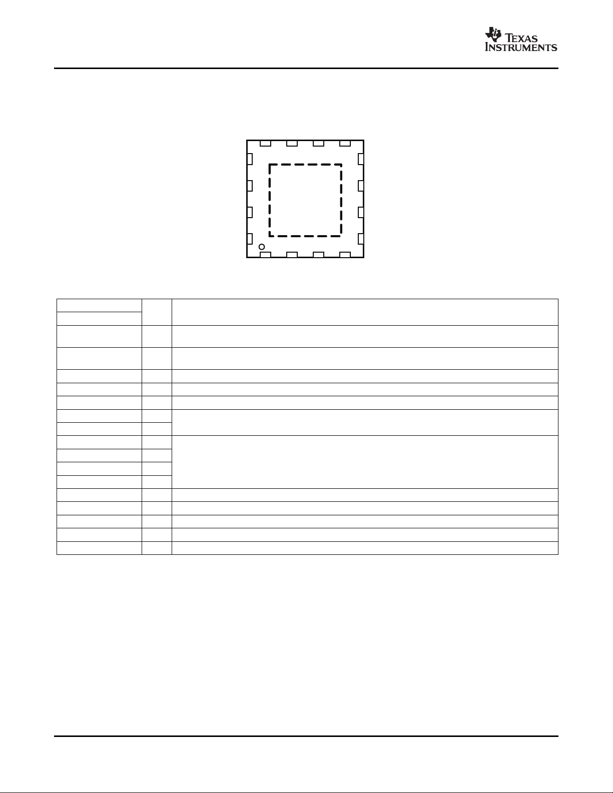
QFN16-PINRTE
3mmX3mm
(TOP VIEW)
TPS60250
SLVS769 – APRIL 2007
PIN ASSIGNMENTS
TERMINAL FUNCTIONS
TERMINAL
NAME NO.
VOUT 1 O
VIN 2 I
SCLK 3 I I2C Interface
SDAT 4 I/O I2C Interface
DM5 5 I Current sink input. Connect the cathode of the aux display or the 5th main display white LED to this pin.
DS1 6 I
DS2 7 I
DM1 8 I
DM2 9 I
DM3 10 I
DM4 11 I
GND 12 – Ground
C1– 13 – Connect to the flying capacitor C1
C2+ 14 – Connect to the flying capacitor C2
C2– 15 – Connect to the flying capacitor C2
C1+ 16 – Connect to the flying capacitor C1
I/O DESCRIPTION
Connect the anodes of the sub, main, and aux display white LEDs to this pin. Bypass decouple VOUT to
GND with a 4.7- µ F or greater ceramic capacitor.
Supply voltage input. Connect to a 3-V to 6-V input supply source. Bypass VIN to GND with a 1- µ F or
greater ceramic capacitor.
Current sink input. Connect the cathode of one of the sub display white LEDs to this pin.
Current sink input. Connect the cathode of one of the main display white LED to this pin.
4
Submit Documentation Feedback
www.ti.com
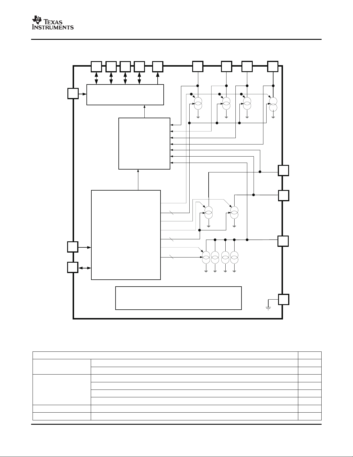
FUNCTIONAL BLOCK DIAGRAM
5
DM5
6
DS1
7 DS2
11 10 9 8
DM 4 DM 3 DM 2 DM 1
GEAR
CONTROL
&
OPENLAMP
DETECTION
1X, 1.5XCHARGEPUMP
1
VOUT
13141516
C
1
-
C
2
+
C
2
-
C
1
+
2
VIN
I2C
INTERFACE
ENmain
MainDimming
ENsub 1
ENsub 2
SubDimming
ENaux
AUXDimming
SCLK
SDAT 4
3
6
6
6
12 GND
BIAS, TEST,& MONITORING
ENold
TPS60250
SLVS769 – APRIL 2007
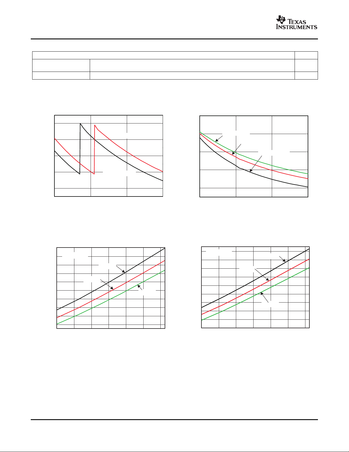
TABLE OF GRAPHS
Efficiency
Output Impedance of × 1
and × 1.5 Mode
Shutdown Current Shutdown Current vs Input Voltage Figure 9
Input Current Input Current vs Supply Voltage, 4 Main LED Figure 10
Efficiency vs Input Voltage, 4 Main LED - 15mA, 25mA Figure 3
Efficiency vs Input Voltage, 2 Sub LED with Light Load Condition, × 1 Mode Operation Figure 4
Switch Resistance vs Free-Air Temperature, × 1 Mode, I
Switch Resistance vs Free-Air Temperature, × 1 Mode, I
Switch Resistance vs Free-Air Temperature, × 1.5 Mode Charge Pump Open-Loop , I
Switch Resistance vs Free-Air Temperature, × 1.5 Mode Charge Pump Open-Loop, I
TYPICAL CHARACTERISTICS
DESCRIPTION REF
= 230 mA Figure 5
LED
= 100 mA Figure 6
LED
= 230 mA Figure 7
LED
= 100 mA Figure 8
LED
Submit Documentation Feedback
5
www.ti.com
90
80
70
60
50
Efficiency-%
3 4 5 6
V -InputVoltage-V
I
15mA,V =3.43V
F
25mA,V =3.79V
F
100
80
40
60
20
Efficiency-%
3 4 5 6
V -InputVoltage-V
I
0.2mA,V =2.6V
F
1mA,V =2.8V
F
0.5mA,V =2.7V
F
-40 -20 0 20 40 60 80
0.65
0.70
0.75
0.80
0.85
0.90
0.95
1
1.05
1.10
SwitchResistance- W
T -Free-AirTemperature-°C
A
I
LED
=100mA
V =3.6V
I
V =3.9V
I
V =3.3V
I
-40 -20 0 20 40 60 80
0.70
0.75
0.80
0.85
0.90
0.95
1
1.05
1.10
1.15
T -Free-AirTemperature-°C
A
V =3.6V
I
V =3.9V
I
I
LED
=230mA
V =3.3V
I
SwitchResistance- W
TPS60250
SLVS769 – APRIL 2007
TYPICAL CHARACTERISTICS (continued)
DESCRIPTION REF
DM5 with Maximum 80
mA
Current Accuracy WLED Current vs Input Voltage, 4 Main LED with 15 mA Figure 12
DM5 Current vs Input Voltage, Programmed with 80 mA Figure 11
EFFICIENCY vs
vs INPUT VOLTAGE
INPUT VOLTAGE (2 Sub LED with Light Load Condition,
(4 Main LED - 15mA, 25mA) × 1 Mode Operation)
Figure 3. Figure 4.
SWITCH RESISTANCE SWITCH RESISTANCE
vs vs
FREE-AIR TEMPERATURE FREE-AIR TEMPERATURE
( × 1 Mode) ( × 1 Mode)
EFFICIENCY
6
Figure 5. Figure 6.
Submit Documentation Feedback
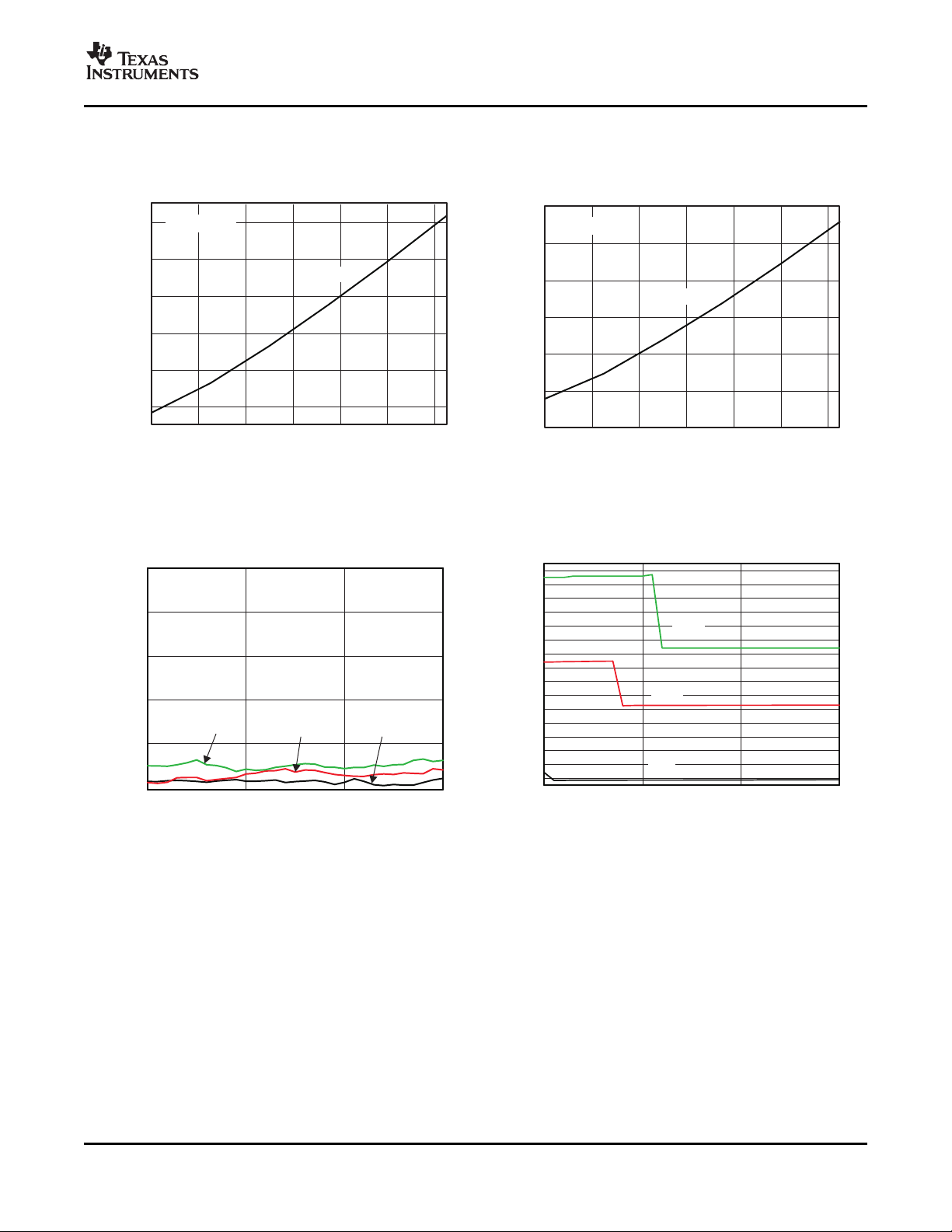
www.ti.com
-40
-20
0
20
40 60 80
2.8
3
3.2
3.4
3.6
3.8
I
LED
=230mA
V =3V
I
SwitchResistance- W
T -Free-AirTemperature-°C
A
-40 -20 0 20 40 60 80
2.6
2.8
3
3.2
3.4
3.6
3.8
SwitchResistance-
W
T -Free-AirTemperature-°C
A
I
LED
=100mA
V =3V
I
0.16
0.15
0.14
0.13
0.12
0.11
0.10
0.09
0.08
0.07
0.06
0.05
0.04
0.03
0.02
0.01
I
-InputCurrent- A
CC
3
4
5
6
V -InputVoltage-V
I
25mA
15mA
2mA
10
8
6
4
2
0
ShutdownCurrent- Am
3
4
5
6
V -InputVoltage-V
I
T =85°C
A
T =25°C
A
T =-40°C
A
TPS60250
SLVS769 – APRIL 2007
SWITCH RESISTANCE SWITCH RESISTANCE
vs vs
FREE-AIR TEMPERATURE FREE-AIR TEMPERATURE
( × 1.5 Mode Charge Pump Open-Loop) ( × 1.5 Mode Charge Pump Open-Loop)
Figure 7. Figure 8.
INPUT CURRENT
SHUTDOWN CURRENT vs
vs SUPPLY VOLTAGE
INPUT VOLTAGE (4 Main LED)
Figure 9. Figure 10.
Submit Documentation Feedback
7

www.ti.com
2.5 3 3.5 4
0
0.01
0.02
0.03
0.04
0.05
0.06
0.07
0.08
V -InputVoltage-V
I
0.3V
0.15V
0.1V
0.05V
0.4V
0.35V
0.25V
0.2V
DM5Current- A
0.016
0.014
0.012
0.010
3 4 5 6
V -InputVoltage-V
I
WLEDCurrent-
A
IDM3IDM2
IDM1
IDM4
TPS60250
SLVS769 – APRIL 2007
DM5 CURRENT WLED CURRENT
vs vs
INPUT VOLTAGE INPUT VOLTAGE
(Programmed with 80 mA) (4 Main LED with 15 mA)
Figure 11. Figure 12.
8
Submit Documentation Feedback

www.ti.com
TPS60250
SLVS769 – APRIL 2007
APPLICATION INFORMATION
APPLICATION OVERVIEW
Most of the current handsets fall into one of three categories. First is the clamshell design, with a main display
on the inside, a secondary display on the outside and a keypad backlight. Second is the bar design, with a main
display and a keypad backlight. Third is the slide type (slide-up and slide-down) design, with a main display and
two keypad banks (inside and outside). The TPS60250 is well suited for use in these three major phone designs
because it has 7 individually regulated white LED current paths and that drive up to five white LEDs in main
display and up to two white LEDs in sub display with regulated constant current for uniform intensity. The main
and sub display LED channels drive up to 25mA and an auxiliary LED output (DM5) drives up to 80mA that can
be assigned for keypad backlight, torch light or low cost/weak camera flash application using I2C interface.
The TPS60250 circuit uses only 4 external components: the input/output capacitors and 2 chargepump flying
capacitors. The few external components combined with the small 3mm × 3mm QFN package provide for a small
total solution size. By combining independent control of three separate banks of backlight LEDs with low cost
and weak flash capability, the TPS60250 helps designers minimize power consumption especially in case of
light load condition while reducing component count and package size.
OPERATING PRINCIPLE
Charge pumps are becoming increasingly attractive in battery-operated applications where board space and
maximum height of the converter are critical constraints. The major advantage of a charge pump is the use of
only capacitors as storage elements. The TPS60250 chargepump provides regulated LED current from a 3-V to
6-V input source. It operates in two modes. The 1 × mode, where the input is connected to the output through a
pass element, and a high efficiency 1.5 × charge pump mode. The IC maximizes power efficiency by operating in
1 × and 1.5 × modes as input voltage and LED current conditions require. The mode of operation is automatically
selected by comparing the forward voltage of the WLED plus the voltage of current sink for each LED with the
input voltage. The IC starts up in 1 × mode, and automatically transitions to 1.5 × if the voltage at any current sink
input (DM_or DS_) falls below the 100-mV transition voltage. The IC returns to 1 × mode as the input rises.
Figure 13 provides a visual explanation of the 1 × to 1.5 × transition.
In 1.5 × mode, the internal oscillator determines the charge/discharge cycles for the flying capacitors. During a
charge cycle, the flying capacitors are connected in series and charged up to the input voltage. After the on-time
of the internal oscillator expires, the flying capacitors are reconfigured to be in parallel and then connected in
series to the input voltage. This provides an output of 1.5 × the input voltage. After the off-time of the internal
oscillator expires, another charge cycle initiates and the process repeats.
Submit Documentation Feedback
9

www.ti.com
x1Operating
Area
x1.5
Operating
Area
V
I
V
I
V
O
V
A
V
F
V
DX
CP WLEDDriver
V
B
V
C
V
HYS
TPS60250
SLVS769 – APRIL 2007
APPLICATION INFORMATION (continued)
Figure 13. Input Voltage Hysteresis Between × 1 and × 1.5 Mode
As shown in Figure 13 , there is input voltage hysteresis voltage between 1 × and 1.5 × mode to ensure stable
operation during mode transition. For the 1 cell Li-Ion battery input voltage range, the TPS60250 operates in 1 ×
mode when a fully charged battery is installed. Once the battery voltage drops below the V
level, which is the
B
mode transition voltage from 1 × to 1.5 × , the WLED driver operates in 1.5 × mode. Once in 1.5 × mode, the battery
voltage must rise to the V
level in order to transition from 1.5 × to 1 × . This hysteresis ensures stable operation
C
when there is some input voltage fluctuation at the 1 × /1.5 × mode transition. The WLED driver provides a typical
280mV hysteresis voltage (V
The transition voltage, VB, depends on V
drop) and V
V
B
V
A
Where R
impedance specifications.
The TPS60250 switches up to 1.5 × mode when the input voltage is below V
(the drop out voltage of the charge pump stage) and is calculated as follows:
A
= V
+ V
A
= R
OUT1X
OUT1X
+ V
F
DX
× I
LEDTOTAL
is the 1 × mode output impedance of the IC. See the Electrical Characteristics table for output
as the input is lower than VC. 1.5 × Mode is exited when the input voltage rises above VC. V
V
= V
C
+ 470 mV
F
The input voltage mode transition hysteresis voltage (V
) that changes based on LED current, to prevent oscillating between modes.
HYS
(the mode transition threshold voltage), V
DX
and remains in 1.5 × mode as long
B
) between 1 × and 1.5 × is calculated using the
HYS
(WLED forward voltage
F
is calculated as:
C
following equation.
V
HYS
Note that V
= VC– V
A
= 520 mV – V
B
– VA, where V
DX
is the key factor in determining V
= 100mV
DX
and is dependant on the 1 × mode charge pump output
HYS
impedance and WLED current.
10
Submit Documentation Feedback

www.ti.com
TPS60250
SLVS769 – APRIL 2007
APPLICATION INFORMATION (continued)
LED CURRENT SINKS (DM_, DS_)
The TPS60250 has constant current sinks which drive seven individual LED current paths. Each current sink
regulates the LED current to a constant value determined by the I2C interface. The internal register addressing
allows the LED main channels DM1~DM5 to be controlled independently from the LED sub channels DS1~DS2.
All the LED channels sink up to 25mA of current except DM5 which has an 80-mA maximum current when
configured as an auxiliary output. Using the I2C interface, the user may assign DM5 to the main display bank
with up to 25-mA current or as an auxiliary output for torch or keypad light or low/weak camera flash with 80-mA
current. DM5 has 64 dimming steps same as main and sub display banks when assigned to the main display.
However, it has its own current programming register and enable control. When assigned as an auxiliary, DM5
has 4 dimming steps (full scale, 70%, 40%, 20%).
These optimized current sinks minimize the voltage headroom required to drive each LED and maximize power
efficiency by increasing the amount of time the controller stays in 1 × mode before transitioning to 1.5 × mode.
OPEN LAMP DETECTION
In system production it is often necessary to leave LED current paths open depending on the phone model. For
example, one phone may use 2 LEDs to backlight the main display while another uses 4 LEDs. Rather than use
two different ICs for these different phone applications, the TPS60250 may be used in both applications with no
additional efficiency loss in the 2 LED applications. In traditional LED driver applications when an LED current
path is open, the current sink voltage falls to ground and the current regulation circuitry drives the output to a
maximum voltage in an attempt to regulate the current for the missing LED path. This severely reduces the
system efficiency. The TPS60250 uses 7 internal comparators to detect when one or more open LED condition
occurs and shut down prevent it from forcing the device to gear up the open current sink. The open lamp
detection is enabled/disabled using the I2C interface.
CAPACITOR SELECTION
The TPS60250 is optimized to work with ceramic capacitors with a dielectric of X5R or better. The two flying
capacitors must be the same value for proper operation. The 750-kHz switching frequency requires that the
flying capacitor be less than 4.7 µ F. Use of 1- µ F ceramic capacitors for both chargepump flying capacitors is
recommended.
For good input voltage filtering, low ESR ceramic capacitors are recommended. A 1- µ F ceramic input capacitor
is sufficient for most of the applications. For better input voltage filtering this value can be increased.
The output capacitor controls the amount of ripple on the output. Since small ripple is undetectable by the
human eye, a 4.7- µ F output capacitor works well. If better output filtering and lower ripple is desired, a larger
output capacitor may be used.
SETTING THE LED CURRENT
Figure 14. Dimming Steps for Sub, Main, and Keypad Backlight
Submit Documentation Feedback
11

www.ti.com
Dataline
stable;
datavalid
DATA
CLK
Change
ofdata
allowed
STARTCondition
DATA
CLK
STOP Condition
S P
CE
TPS60250
SLVS769 – APRIL 2007
APPLICATION INFORMATION (continued)
Figure 14 shows the dimming steps for sub, main, and auxiliary display banks in the 25mA maximum current
application. In order to satisfy today's requirement on LED current, the TPS60250 covers low LED current area
from 100 µ A to 1.5mA with 100- µ A dimming step (total 16 steps for 25-mA maximum current) for the new LCD
panels which have improved transparency rates. For LED currents in the range from 2mA to 25mA, the device
uses 48 dimming steps with 0.5mA step. Also, DM5 has 4 dimming steps once the current path is assigned for
auxiliary applications with maximum 80-mA current.
SERIAL INTERFACE
The serial interface is compatible with the standard and fast mode I2C specifications, allowing transfers at up to
400 kHz. The interface adds flexibility to the WLED driver solution, enabling most functions to be programmed to
new values depending on the instantaneous application requirements. Register contents remain intact as long
as V
For normal data transfer, DATA is allowed to change only when CLK is low. Changes when CLK is high are
reserved for indicating the start and stop conditions. During data transfer, the data line must remain stable
whenever the clock line is high. There is one clock pulse per bit of data. Each data transfer is initiated with a
start condition and terminated with a stop condition. When addressed, the TPS60250 device generates an
acknowledge bit after the reception of each byte. The master device (microprocessor) must generate an extra
clock pulse that is associated with the acknowledge bit. The TPS60250 device must pull down the DATA line
during the acknowledge clock pulse so that the DATA line is a stable low during the high period of the
acknowledge clock pulse. Setup and hold times must be taken into account. During read operations, a master
must signal the end of data to the slave by not generating an acknowledge bit on the last byte that was clocked
out of the slave. In this case, the slave TPS60250 device must leave the data line high to enable the master to
generate the stop condition.
remains above UVLO2 (typical 1.3V).
CC
Figure 15. Bit Transfer on the Serial Interface
Figure 16. START and STOP Conditions
12
Submit Documentation Feedback

www.ti.com
SCLK
... ......
SDAT
Slave Address DataRegister Address
.........
A6 R6 R5 R0
AC
K
D7 D6 D5 D0
AC
K
R7
AC
K
R/WA0A4A5
0 0 0 0
StopStart
NOTE: SLAVE=TPS60250
SCLK
... ......
SDAT
Slave Address Slave Address
Register
Address
....
A6 R0
AC
K
R7
AC
K
R/WA0
0 0 0 0
Stop
Start
NOTE: SLAVE=TPS60250
...
..
AC
K
D0D7
AC
K
R/WA0A6
1
Slave
Drives
theData
Master
Drives
ACKandStop
Repeated
Start
..
APPLICATION INFORMATION (continued)
Figure 17. Serial I/F READ From TPS60250: Protocol A
TPS60250
SLVS769 – APRIL 2007
Figure 18. Serial I/F READ From TPS60250: Protocol B
Figure 19. Serial I/F Timing Diagram
The I2C interface uses a combined protocol in which the START condition and the Slave Address are both
repeated. The TPS60250 provides 2 I2C Slave Address using internal EEPROM in case more than 1 device is
used in the system. The primary I2C Slave Address is 1110111. For alternative I2C address, contact the factory.
Submit Documentation Feedback
13

www.ti.com
TPS60250
SLVS769 – APRIL 2007
APPLICATION INFORMATION (continued)
Enable Control Register (Address: 0x00h)
ENABLE B7 B6 B5 B4 B3 B2 B1 B0
BIT NAME X ENold ENmain ENsub2 ENsub1 ENaux DM5H DM5L
Bit 6 ENold (Enable Open Lamp Detection)
1: Open Lamp Detection Enabled
0: Open Lamp Detection Disabled
Bit 5 ENmain
1: Enable Main Display LEDs (DM1-DM4)
0: Disable Main Display LEDs
Bit 4 ENsub2
1: Enable Sub Display LED 2 (DS2)
0: Disable Sub Display LED 2
Bit 3 ENsub1
1: Enable Sub Display LED 1 (DS1)
0: Disable Sub Display LED 1
Bit 2 ENaux
1: Enable Aux Display LED (DM5)
0: Disable Aux Display LED
Bits 1,0 DM5H, DM5L
DM5H DM5L
(B1) (B0)
0 0 Shutdown mode. All outputs disabled, all internal registers set to 0x00h
0 1 Enable the IC and Group DM5 as main display with maximum current of 25mA
1 0 Enable the IC and set DM5 as Aux output with maximum current of 80mA.
Dimming steps determined by Iaux0 and Iaux1 bits.
1 1 Shutdown mode. All outputs disabled, all internal registers set to 0x00h
DM5 Mode and Shutdown Mode
Sub Display Current Control Register (Address: 0x01h)
SUB DISP
CURRENT
BIT NAME X X Isub5 Isub4 Isub3 Isub2 Isub1 Isub0
B7 B6 B5 B4 B3 B2 B1 B0
Bits 5 - 0 Isub5 - Isub0 (total 64 steps)
6-Bit command (64 steps) to these bits sets the current for DS1 and DS2.
For LED currents between 0 and 1.5mA, one step = 0.1mA increment
For LED currents between 1.5 and 25.5mA, one step = 0.5mA increment
Main Display Current Control Register (Address: 0x02h)
MAIN DISP
CURRENT
BIT NAME X X Imain5 Imain4 Imain3 Imain2 Imain1 Imain0
B7 B6 B5 B4 B3 B2 B1 B0
Bits 5 - 0 Imain5 - Imain0 (total 64 steps)
6-Bit command (64 steps) to these bits sets the current for DM1-DM4.
For LED currents between 0 and 1.5mA, one step = 0.1mA increment
For LED currents between 1.5 and 25.5mA, one step = 0.5mA increment
14
Submit Documentation Feedback

www.ti.com
Aux Output Brightness and Operation Mode Control Register (Address: 0x03h)
AUX DISP
CURRENT
BIT NAME Iaux5 Iaux4 Iaux3 Iaux2 Iaux1 Iaux0 Mode1 Mode0
B7 B6 B5 B4 B3 B2 B1 B0
Bits 7 - 2 (DM5 set to Main Display Mode)
Iaux5 - Iaux0 (total 64 steps)
6-Bit command (64 steps) to these bits sets the current for DM5.
For LED currents between 0 and 1.5mA, one step = 0.1mA increment
For LED currents between 1.5 and 25.5mA, one step = 0.5mA increment
Bits 7 - 2 (DM5 set to Aux Display Mode)
Iaux5 Iaux4 Iaux3 Iaux2 Iaux1 Iaux0 Aux Dimming
(B7) (B6) (B5) (B4) (B3) (B2) Step
X X X X 0 0 20%
X X X X 0 1 40%
X X X X 1 0 70%
X X X X 1 1 100%
TPS60250
SLVS769 – APRIL 2007
Bits 1,0 Mode1, Mode0
Mode1 Mode0
(B1) (B0)
TPS60250 Mode
0 0 Auto-Switchover Mode. The TPS60250 selects
1 × /1.5 × mode as described in the Operating Principle
section.
0 1 1 × Mode. TPS60250 remains in 1 × mode regardless
of the input voltage. LED current may not regulate at
lower input voltages when in this mode.
1 0 1.5 × Mode. TPS60250 remains in 1.5 × mode
regardless of the input voltage.
1 1 Auto-Switchover Mode. The TPS60250 selects
1 × /1.5 × mode as described in the Operating Principle
section.
Submit Documentation Feedback
15

www.ti.com
C1-
C2+
C2-
C1+
DM1
DM5
DS2
DS1
DM3DM4 DM2GND
SDATSCLKVIN
C1
1
mF
C2
1
mF
C3
1
mF
MainDisplay
C4
4.7
mF
SubDisplay
I2CInterface
On/Off, DigitalDimming
VOUT
h
Light
+
IO V
F
V
in
ǒ
IO) I
op
Ǔ
TPS60250
SLVS769 – APRIL 2007
APPLICATION CIRCUITS
Figure 20. The Typical Application Circuit for Sub and Main Display
As shown in Figure 20 , this is a typical application circuit for a clam shell phone with 5 main LEDs and 2 sub
LEDs. Recently, the LCD panel makers have developed a new panel that has improved the transparency rate
which makes the system efficiency with a 100- µ A LED current a critical load point. To meet system efficiency
requirements with the light load conditions for the new LCD operating panel, the TPS60250 has a maximum
55- µ A operating current with the 100- µ A output load condition. In this application, the controller always operates
in 1 × mode due to the WLED's low forward voltage drop (about 2.6V
with a 100- µ A WLED current). Thus, the
F
total efficiency at a light load condition is determined using Equation 1 :
Where:
IO: Output Load (WLED) Current
VF: Forward Voltage Drop of WLED
Vin: Input Voltage
Iop: Operating Current of LED Driver
(1)
16
Submit Documentation Feedback

www.ti.com
C1-
C2+
C2-
C1+
DM1
DM5
DS2
DS1
DM3DM 4 DM2GND
SDATSCLKVIN
C1
1uF
C2
1mFC31mF
MainDisplay
C4
4.7mF
SubDisplay
I2CInterface
On/Off, DigitalDimming
VOUT
AuxiliaryPortforKeyPad
orFlashLight
TPS60250
SLVS769 – APRIL 2007
Figure 21. The Typical Application Circuit for Sub, Main, and Keypad Backlight
Figure 21 shows the typical application circuit for sub, main, and keypad backlight. In this application, DM5 is
assigned as the auxiliary input for the keypad lighting application.
LAYOUT GUIDELINES
There are several points to consider when laying out a PCB for charge pump based solutions. In general, all
capacitors should be as close as possible to the device. This is especially important when placing the flying
capacitors (C2, C3 in Figure 20 and Figure 21 ). In cases where DM5 is assigned for torch/flash applications,
with a maximum 80-mA WLED current, this current path must be kept wide to reduce the trace resistance.
Submit Documentation Feedback
17

PACKAGE OPTION ADDENDUM
www.ti.com
7-May-2007
PACKAGING INFORMATION
Orderable Device Status
(1)
Package
Type
Package
Drawing
Pins Package
Qty
Eco Plan
TPS60250RTER ACTIVE QFN RTE 16 3000 Green (RoHS &
no Sb/Br)
TPS60250RTET ACTIVE QFN RTE 16 250 Green (RoHS &
no Sb/Br)
(1)
The marketing status values are defined as follows:
ACTIVE: Product device recommended for new designs.
LIFEBUY: TI has announced that the device will be discontinued, and a lifetime-buy period is in effect.
NRND: Not recommended for new designs. Device is in production to support existing customers, but TI does not recommend using this part in
a new design.
PREVIEW: Device has been announced but is not in production. Samples may or may not be available.
OBSOLETE: TI has discontinued the production of the device.
(2)
Eco Plan - The planned eco-friendly classification: Pb-Free (RoHS), Pb-Free (RoHS Exempt), or Green (RoHS & no Sb/Br) - please check
http://www.ti.com/productcontent for the latest availability information and additional product content details.
TBD: The Pb-Free/Green conversion plan has not been defined.
Pb-Free (RoHS): TI's terms "Lead-Free" or "Pb-Free" mean semiconductor products that are compatible with the current RoHS requirements
for all 6 substances, including the requirement that lead not exceed 0.1% by weight in homogeneous materials. Where designed to be soldered
at high temperatures, TI Pb-Free products are suitable for use in specified lead-free processes.
Pb-Free (RoHS Exempt): This component has a RoHS exemption for either 1) lead-based flip-chip solder bumps used between the die and
package, or 2) lead-based die adhesive used between the die and leadframe. The component is otherwise considered Pb-Free (RoHS
compatible) as defined above.
Green (RoHS & no Sb/Br): TI defines "Green" to mean Pb-Free (RoHS compatible), and free of Bromine (Br) and Antimony (Sb) based flame
retardants (Br or Sb do not exceed 0.1% by weight in homogeneous material)
(2)
Lead/Ball Finish MSL Peak Temp
CU NIPDAU Level-2-260C-1 YEAR
CU NIPDAU Level-2-260C-1 YEAR
(3)
(3)
MSL, Peak Temp. -- The Moisture Sensitivity Level rating according to the JEDEC industry standard classifications, and peak solder
temperature.
Important Information and Disclaimer:The information provided on this page represents TI's knowledge and belief as of the date that it is
provided. TI bases its knowledge and belief on information provided by third parties, and makes no representation or warranty as to the
accuracy of such information. Efforts are underway to better integrate information from third parties. TI has taken and continues to take
reasonable steps to provide representative and accurate information but may not have conducted destructive testing or chemical analysis on
incoming materials and chemicals. TI and TI suppliers consider certain information to be proprietary, and thus CAS numbers and other limited
information may not be available for release.
In no event shall TI's liability arising out of such information exceed the total purchase price of the TI part(s) at issue in this document sold by TI
to Customer on an annual basis.
Addendum-Page 1

PACKAGE MATERIALS INFORMATION
www.ti.com
2-Jul-2007
TAPE AND REEL INFORMATION
Pack Materials-Page 1

PACKAGE MATERIALS INFORMATION
www.ti.com
Device Package Pins Site Reel
Diameter
(mm)
TPS60250RTER RTE 16 MLA 330 12 3.3 3.3 1.1 8 12 Q2
TPS60250RTET RTE 16 MLA 180 12 3.3 3.3 1.1 8 12 Q2
Reel
Width
(mm)
A0 (mm) B0 (mm) K0 (mm) P1
(mm)W(mm)
2-Jul-2007
Pin1
Quadrant
TAPE AND REEL BOX INFORMATION
Device Package Pins Site Length (mm) Width (mm) Height (mm)
TPS60250RTER RTE 16 MLA 346.0 346.0 29.0
TPS60250RTET RTE 16 MLA 190.0 212.7 31.75
Pack Materials-Page 2


IMPORTANT NOTICE
Texas Instruments Incorporated and its subsidiaries (TI) reserve the right to make corrections, modifications, enhancements,
improvements, and other changes to its products and services at any time and to discontinue any product or service without notice.
Customers should obtain the latest relevant information before placing orders and should verify that such information is current and
complete. All products are sold subject to TI’s terms and conditions of sale supplied at the time of order acknowledgment.
TI warrants performance of its hardware products to the specifications applicable at the time of sale in accordance with TI’s
standard warranty. Testing and other quality control techniques are used to the extent TI deems necessary to support this
warranty. Except where mandated by government requirements, testing of all parameters of each product is not necessarily
performed.
TI assumes no liability for applications assistance or customer product design. Customers are responsible for their products and
applications using TI components. To minimize the risks associated with customer products and applications, customers should
provide adequate design and operating safeguards.
TI does not warrant or represent that any license, either express or implied, is granted under any TI patent right, copyright, mask
work right, or other TI intellectual property right relating to any combination, machine, or process in which TI products or services
are used. Information published by TI regarding third-party products or services does not constitute a license from TI to use such
products or services or a warranty or endorsement thereof. Use of such information may require a license from a third party under
the patents or other intellectual property of the third party, or a license from TI under the patents or other intellectual property of TI.
Reproduction of TI information in TI data books or data sheets is permissible only if reproduction is without alteration and is
accompanied by all associated warranties, conditions, limitations, and notices. Reproduction of this information with alteration is an
unfair and deceptive business practice. TI is not responsible or liable for such altered documentation. Information of third parties
may be subject to additional restrictions.
Resale of TI products or services with statements different from or beyond the parameters stated by TI for that product or service
voids all express and any implied warranties for the associated TI product or service and is an unfair and deceptive business
practice. TI is not responsible or liable for any such statements.
TI products are not authorized for use in safety-critical applications (such as life support) where a failure of the TI product would
reasonably be expected to cause severe personal injury or death, unless officers of the parties have executed an agreement
specifically governing such use. Buyers represent that they have all necessary expertise in the safety and regulatory ramifications
of their applications, and acknowledge and agree that they are solely responsible for all legal, regulatory and safety-related
requirements concerning their products and any use of TI products in such safety-critical applications, notwithstanding any
applications-related information or support that may be provided by TI. Further, Buyers must fully indemnify TI and its
representatives against any damages arising out of the use of TI products in such safety-critical applications.
TI products are neither designed nor intended for use in military/aerospace applications or environments unless the TI products are
specifically designated by TI as military-grade or "enhanced plastic." Only products designated by TI as military-grade meet military
specifications. Buyers acknowledge and agree that any such use of TI products which TI has not designated as military-grade is
solely at the Buyer's risk, and that they are solely responsible for compliance with all legal and regulatory requirements in
connection with such use.
TI products are neither designed nor intended for use in automotive applications or environments unless the specific TI products
are designated by TI as compliant with ISO/TS 16949 requirements. Buyers acknowledge and agree that, if they use any
non-designated products in automotive applications, TI will not be responsible for any failure to meet such requirements.
Following are URLs where you can obtain information on other Texas Instruments products and application solutions:
Products Applications
Amplifiers amplifier.ti.com Audio www.ti.com/audio
Data Converters dataconverter.ti.com Automotive www.ti.com/automotive
DSP dsp.ti.com Broadband www.ti.com/broadband
Interface interface.ti.com Digital Control www.ti.com/digitalcontrol
Logic logic.ti.com Military www.ti.com/military
Power Mgmt power.ti.com Optical Networking www.ti.com/opticalnetwork
Microcontrollers microcontroller.ti.com Security www.ti.com/security
RFID www.ti-rfid.com Telephony www.ti.com/telephony
Low Power www.ti.com/lpw Video & Imaging www.ti.com/video
Wireless
Wireless www.ti.com/wireless
Mailing Address: Texas Instruments, Post Office Box 655303, Dallas, Texas 75265
Copyright © 2007, Texas Instruments Incorporated
 Loading...