

Page 1

User’s Guide
July 2004
PMP Portable Power Products
SBVU008
Page 2

IMPORTANT NOTICE
Texas Instruments Incorporated and its subsidiaries (TI) reserve the right to make corrections, modifications,
enhancements, improvements, and other changes to its products and services at any time and to discontinue
any product or service without notice. Customers should obtain the latest relevant information before placing
orders and should verify that such information is current and complete. All products are sold subject to TI’s terms
and conditions of sale supplied at the time of order acknowledgment.
TI warrants performance of its hardware products to the specifications applicable at the time of sale in
accordance with TI’s standard warranty. Testing and other quality control techniques are used to the extent TI
deems necessary to support this warranty . Except where mandated by government requirements, testing of all
parameters of each product is not necessarily performed.
TI assumes no liability for applications assistance or customer product design. Customers are responsible for
their products and applications using TI components. To minimize the risks associated with customer products
and applications, customers should provide adequate design and operating safeguards.
TI does not warrant or represent that any license, either express or implied, is granted under any TI patent right,
copyright, mask work right, or other TI intellectual property right relating to any combination, machine, or process
in which TI products or services are used. Information published by TI regarding third-party products or services
does not constitute a license from TI to use such products or services or a warranty or endorsement thereof.
Use of such information may require a license from a third party under the patents or other intellectual property
of the third party, or a license from TI under the patents or other intellectual property of TI.
Reproduction of information in TI data books or data sheets is permissible only if reproduction is without
alteration and is accompanied by all associated warranties, conditions, limitations, and notices. Reproduction
of this information with alteration is an unfair and deceptive business practice. TI is not responsible or liable for
such altered documentation.
Resale of TI products or services with statements different from or beyond the parameters stated by TI for that
product or service voids all express and any implied warranties for the associated TI product or service and
is an unfair and deceptive business practice. TI is not responsible or liable for any such statements.
Following are URLs where you can obtain information on other Texas Instruments products and application
solutions:
Products Applications
Amplifiers amplifier.ti.com Audio www.ti.com/audio
Data Converters dataconverter.ti.com Automotive www.ti.com/automotive
DSP dsp.ti.com Broadband www.ti.com/broadband
Interface interface.ti.com Digital Control www.ti.com/digitalcontrol
Logic logic.ti.com Military www.ti.com/military
Power Mgmt power.ti.com Optical Networking www.ti.com/opticalnetwork
Microcontrollers microcontroller.ti.com Security www.ti.com/security
Telephony www.ti.com/telephony
Video & Imaging www.ti.com/video
Wireless www.ti.com/wireless
Mailing Address: Texas Instruments
Post Office Box 655303 Dallas, Texas 75265
Copyright 2004, Texas Instruments Incorporated
Page 3

EVM IMPORTANT NOTICE
Texas Instruments (TI) provides the enclosed product(s) under the following conditions:
This evaluation kit being sold by TI is intended for use for ENGINEERING DEVELOPMENT OR EVALUATION
PURPOSES ONLY and is not considered by TI to be fit for commercial use. As such, the goods being provided
may not be complete in terms of required design-, marketing-, and/or manufacturing-related protective
considerations, including product safety measures typically found in the end product incorporating the goods.
As a prototype, this product does not fall within the scope of the European Union directive on electromagnetic
compatibility and therefore may not meet the technical requirements of the directive.
Should this evaluation kit not meet the specifications indicated in the EVM User’s Guide, the kit may be returned
within 30 days from the date of delivery for a full refund. THE FOREGOING WARRANTY IS THE EXCLUSIVE
WARRANTY MADE BY SELLER TO BUYER AND IS IN LIEU OF ALL OTHER WARRANTIES, EXPRESSED,
IMPLIED, OR S TATUTORY, INCLUDING ANY WARRANTY OF MERCHANTABILITY OR FITNESS FOR ANY
PARTICULAR PURPOSE.
The user assumes all responsibility and liability for proper and safe handling of the goods. Further, the user
indemnifies TI from all claims arising from the handling or use of the goods. Please be aware that the products
received may not be regulatory compliant or agency certified (FCC, UL, CE, etc.). Due to the open construction
of the product, it is the user’s responsibility to take any and all appropriate precautions with regard to electrostatic
discharge.
EXCEPT TO THE EXTENT OF THE INDEMNITY SET FORTH ABOVE, NEITHER PARTY SHALL BE LIABLE
TO THE OTHER FOR ANY INDIRECT, SPECIAL, INCIDENTAL, OR CONSEQUENTIAL DAMAGES.
TI currently deals with a variety of customers for products, and therefore our arrangement with the user is not
exclusive.
TI assumes no liability for applications assistance, customer product design, software performance, or
infringement of patents or services described herein.
Please read the EVM User’s Guide and, specifically, the EVM Warnings and Restrictions notice in the EVM
User’s Guide prior to handling the product. This notice contains important safety information about temperatures
and voltages. For further safety concerns, please contact the TI application engineer.
Persons handling the product must have electronics training and observe good laboratory practice standards.
No license is granted under any patent right or other intellectual property right of TI covering or relating to any
machine, process, or combination in which such TI products or services might be or are used.
Mailing Address:
Texas Instruments
Post Office Box 655303
Dallas, Texas 75265
Copyright 2004, Texas Instruments Incorporated
Page 4

EVM WARNINGS AND RESTRICTIONS
It is important to operate this EVM within the input voltage range of 0 V and 7 V.
Exceeding the specified input range may cause unexpected operation and/or irreversible
damage to the EVM. If there are questions concerning the input range, please contact a TI
field representative prior to connecting the input power.
Applying loads outside of the specified output range may result in unintended operation and/or
possible permanent damage to the EVM. Please consult the EVM User’s Guide prior to
connecting any load to the EVM output. If there is uncertainty as to the load specification,
please contact a TI field representative.
During normal operation, some circuit components may have case temperatures greater than
+25°C. The EVM is designed to operate properly with certain components above +25°C as
long as the input and output ranges are maintained. These components include but are not
limited to linear regulators, switching transistors, pass transistors, and current sense
resistors. These types of devices can be identified using the EVM schematic located in the
EVM User’s Guide. When placing measurement probes near these devices during operation,
please be aware that these devices may be very warm to the touch.
Mailing Address:
Texas Instruments
Post Office Box 655303
Dallas, Texas 75265
Copyright 2004, Texas Instruments Incorporated
Page 5

About This Manual
This user’s guide provides the information needed to set up and operate the
TPS60230EVM-047 evaluation module. For a more detailed description of the
TPS60230, please refer to the product data sheet available from the Texas In struments web site at http://www.ti.com
listed in the sections of this guide entitled Related Documentation from Texas
Instruments.
How to Use This Manual
Throughout this document, the acronym EVM and the phrase evaluation
module are synonymous with the TPS60230EVM−047.
Preface
Read This First
. Additional support documents are
Related Documentation From Texas Instruments
The following document(s) provide information regarding Texas Instrument integrated circuits used in the assembly of the TPS60230EVM−047. These documents are available from the TI web site. The last character of the literature
number corresponds to the document revision, which is current at the time of
the writing of this user’s guide. Newer revisions may be available from the TI
web site at http://www.ti.com
sponse Center at (800) 477−8924 or the Product Information Center at (972)
644−5580. When ordering, identify the document(s) by both title and literature
number.
Data Sheets: Literature Number:
TPS60230 SLVS516
or by calling the Texas Instruments Literature Re-
Page 6

Contents
If You Need Assistance
If you have questions regarding either the use of this evaluation module or the
information contained in the accompanying documentation, please contact
your local TI sales representative, the Texas Instruments Product Information
Center at (972) 644−5580, or visit the TI Semiconductor Online Technical Support pages at http://www.ti.com
FCC Warning
This equipment is intended for use in a laboratory test environment only. It may
generate, use, or radiate radio frequency energy and has not been tested for
compliance with the limits of computing devices pursuant to sub−part J of part
15 of the FCC regulations, which are designed to provide reasonable protection against radio frequency interference. Operation of this equipment in other
environments may cause interference with radio communications, in which
case the user at his own expense will be required to take whatever measures
may be required to correct this interference.
Trademarks
.
All trademarks are the property of their respective owners.
iv
Page 7

TPS60230EVMĆ047
This user’s guide describes the characteristics, operation, and use of the
TPS60230EVM-047 LED charge-pump current-source evaluation module
(EVM). This EVM features a high-efficiency charge-pump-based white LED
driver designed to operate off a single cell Li-Ion battery and drive up to five
white LEDs with up to 20mA each. This user’s guide includes setup
instructions, test results, a schematic diagram, a bill of materials (BOM), and
printed circuit board (PCB) layout drawings for the evaluation module.
Topic Page
1 Introduction 2. . . . . . . . . . . . . . . . . . . . . . . . . . . . . . . . . . . . . . . . . . . . . . . . . . . .
2 Initial Configuration 2. . . . . . . . . . . . . . . . . . . . . . . . . . . . . . . . . . . . . . . . . . . . .
3 Printed Circuit Board (PCB) Layout 4. . . . . . . . . . . . . . . . . . . . . . . . . . . . . . .
4 Schematic 5. . . . . . . . . . . . . . . . . . . . . . . . . . . . . . . . . . . . . . . . . . . . . . . . . . . . . .
5 Bill of Materials 5. . . . . . . . . . . . . . . . . . . . . . . . . . . . . . . . . . . . . . . . . . . . . . . . .
TPS60230EVM-047
1
Page 8

Introduction
1 Introduction
The Texas Instruments TPS60230EVM-047 evaluation module (EVM) helps
designers evaluate the operation and performance of the TPS60230. This device is an efficient charge-pump-based current sink that can drive up to five
white LEDs with 25mA each. Efficiency is improved by switching between a
1.0x and 1.5x mode, based on the input voltage.
This EVM is specifically designed and optimized to operate with a single-cell
Li-Ion battery input. The default maximum current setting for this EVM is 20mA
per LED. If desired, this EVM can easily be modified to supply higher or lower
currents by appropriately selecting the ISET resistor, R1. Refer to the data
sheet (SLVS516) for more information on adjusting the LED current.
2 Initial Configuration
This section describes the jumpers and connectors on the EVM, as well as how
to properly connect, set up, and use the TPS60230EVM-047.
2.1 Input/Output Connector Descriptions
2.1.1 J1: VIN
2.1.2 J2: GND
2.1.3 JP1: EN2
2.1.4 JP2: EN1
This is the positive connection to the input power supply or battery.
This is the return connection for the input power supply or battery.
This jumper will ground the EN2 pin or connect it to VIN. If the both EN1 and
EN2 are connected to VIN, the LED current will be the full programmed value
set by R1. For this EVM, that current is 20mA. If EN2 is connected to ground
and EN1 is high, the LED current will be set to 1/3 the programmed value, or
6.66mA. If both EN1 and EN2 are grounded, the LEDs will turn off.
This jumper will ground the EN1 pin or connect it to VIN. If the both EN1 and
EN2 are connected to VIN, the LED current will be the full programmed value
set by R1. For this EVM, that current is 20mA. If EN1 is connected to ground
and EN2 is high, the LED current will be set to 2/3 the programmed value, or
13.33mA. If both EN1 and EN2 are grounded, the LEDs will turn off.
2
Page 9

2.2 Setup
Connect an input supply or battery between J1 and J2. The voltage range on
this supply should stay between 2.7V and 6.0V. Set the appropriate brightness
by configuring JP1 and JP2.
2.3 Operation
The EVM has been optimized to operate from a single-cell Li-Ion battery with
an input voltage range of 2.7V to 6.0V. The value for R1 programs the maximum LED current. For this EVM, the maximum current is set to 20mA. However, by changing the value of R1, LED currents up to 25mA can be achieved.
Currents less than 20mA can be achieved by appropriately configuring JP1
and JP2, as shown in Table 1.
Table 1. Relative LED Current Levels
JP1 (EN2) JP2 (EN1) LED CURRENT
0 0 0
0 1 1/3 full
1 0 2/3 full
1 1 Full (20mA for R1 = 7.87kΩ)
Input/Output Connector Descriptions
EN1 and EN2 can also be used for pulse width modulator (PWM) dimming.
The PWM signal can be applied to EN1, EN2, or both. In this case, the LED
current is proportional to duty factor and can have a maximum current dictated
by how EN1 and EN2 are configured. The maximum recommended PWM frequency is 50kHz, and the minimum recommended ON time is 2.5us. Refer to
the datasheet (SLVS516) for more information in regards to PWM dimming.
2.4 Test Results
The efficiency curve in Figure 1 reflects the power delivered to the LED. The
output power used for the efficiency calculation is the sum of all the LED currents multiplied by the LED forward voltage.
Figure 1. Efficiency vs VIN
90
80
70
60
50
40
Efficiency (%)
30
20
10
0
2.7 3.1 3.5 3.9 4.3 4.7 5.1 5.5 5.9 6.3 6.5
Input Voltage (V)
EN2 and EN1 = On
=20mA
I
LED
TPS60230EVM-047
3
Page 10
Printed Circuit Board (PCB) Layout
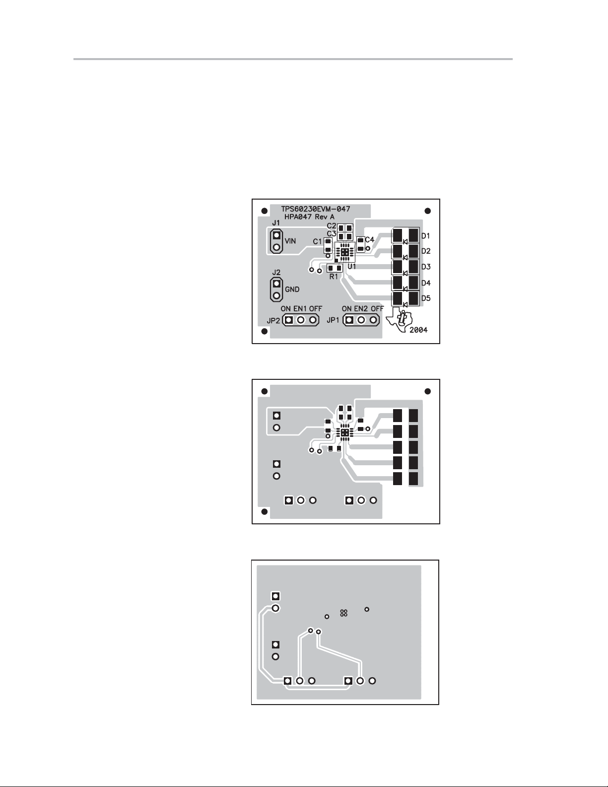
3 Printed Circuit Board (PCB) Layout
PCB layout is critical for all switch-mode power supplies. Figure 2, Figure 3,
and Figure 4 show the board layout for the TPS60230EVM-047 PWB. The
nodes with high switching frequencies and currents are short and are isolated
from the noise-sensitive feedback circuitry. Careful attention has been given
to the routing of high-frequency current loops. Refer to the product datasheet
(SLVS516) for specific layout guidelines.
Figure 2. Assembly Layer
Figure 3. Top Layer Routing
Figure 4. Bottom Layer Routing
4
Page 11

4 Schematic
Figure 5. TPS60230EVM−047 Schematic
Schematic
5 Bill of Materials
Table 2. Bill of Materials
Qty Ref Des Description Size Mfr Part Number
2 C1, C4 Capacitor, ceramic, 1.0µF, 6.3V,
X5R, 10%
2 C2, C3 Capacitor, ceramic, 0.47µF, 10V,
X5R, 10%
5 D1 − D5 Diode, LED, White, 30mA 1210 Lumex SML−LX2832UWC−TR
2 J1, J2 Header, 2-pin, 100mil spacing,
(36-pin strip)
2 JP1, JP2 Header, 3-pin, 100mil spacing,
(36-pin strip)
1 R1 Resistor, chip, 7.87kΩ, 1/16W, 1% 603 Std Std
1 U1 IC, white LED charge pump current
source
1 −− PCB, 1.55 in x 1.195 in x 0.062 in Any HPA047
2 −− Shunt, 100mil, black 0.100 3M 929950−00
603 TDK C1608X5R0J105KT
603 TDK C1608X5R1A474KT
0.100 x 2 Sullins PTC36SAAN
0.100 x 3 Sullins PTC36SAAN
0.80 x 0.80 TI TPS60230RGT
TPS60230EVM-047
5
 Loading...