

TPS60100
REGULATED 3.3 V 200-mA LOW-NOISE
CHARGE PUMP DC/DC CONVERTER
SLVS213B – MAY 1999 – REVISED SEPTEMBER 1999
1
POST OFFICE BOX 655303 • DALLAS, TEXAS 75265
features
D
Up to 200-mA Output Current
D
Less Than 5-mVpp Output Voltage Ripple
D
No Inductors Required/Low EMI
D
Regulated 3.3-V ±4% Output
D
Only Four External Components Required
D
Up to 90% Efficiency
D
1.8-V to 3.6-V Input Voltage Range
D
50-µA Quiescent Supply Current
D
0.05-µA Shutdown Current
D
Load Isolated in Shutdown
D
Space-Saving Thermally-Enhanced TSSOP
PowerPAD Package
D
Evaluation Module Available
(TPS60100EVM–131)
applications
Replaces DC/DC Converters With Inductors in
– Battery-Powered Applications
– Two Battery Cells to 3.3-V Conversion
– Portable Instruments
– Battery-Powered Microprocessor and
DSP Systems
– Miniature Equipment
– Backup-Battery Boost Converters
– PDAs
– Laptops
– Handheld Instrumentation
– Medical Instruments
– Cordless Phones
description
The TPS60100 step-up, regulated charge pump
generates a 3.3-V ±4% output voltage from a
1.8-V to 3.6-V input voltage (two alkaline, NiCd, or
NiMH batteries). Output current is 200 mA from a
2-V input. Only four external capacitors are
needed to build a complete low-noise dc/dc
converter. The push-pull operating mode of two
single-ended charge pumps assures the low
output voltage ripple as current is continuously
transferred to the output. From a 2-V input, the
TPS60100 can start into full load with loads as low
as 16 Ω.
The TPS60100 features either constant frequency mode to minimize noise and output voltage
ripple or the power-saving pulse-skip mode to
extend battery life at light loads. The TPS60100
switching frequency is 300 kHz. The logic
shutdown function reduces the supply current to
1-µA (max) and disconnects the load from the
input. Special current-control circuitry prevents
excessive current from being drawn from the
battery during start-up. This dc/dc converter
requires no inductors and has low EMI. It is
available in the small 20-pin TSSOP PowerP AD
package (PWP).
Copyright 1999, Texas Instruments Incorporated
PRODUCTION DATA information is current as of publication date.
Products conform to specifications per the terms of Texas Instruments
standard warranty. Production processing does not necessarily include
testing of all parameters.
Please be aware that an important notice concerning availability, standard warranty, and use in critical applications of
Texas Instruments semiconductor products and disclaimers thereto appears at the end of this data sheet.
PowerPAD is a trademark of Texas Instruments Incorporated.
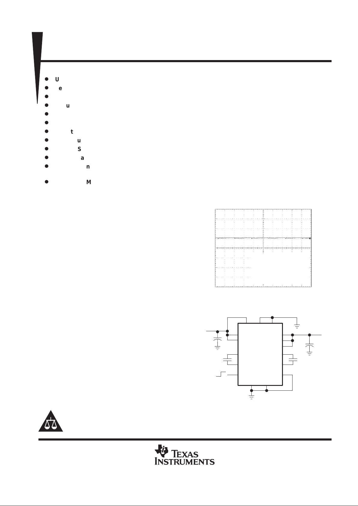
output voltage ripple
typical operating circuit
Figure 1
3.45
10
3.25
3.3
3.35
3.4
3.05
3.1
3.15
3.2
501234 6789
t – Time – µs
– Output Voltage – VV
O
SKIP =COM = 3V8 = 0 V
VIN = 2.4 V
IO = 200 mA
CO = 22 µF
X5R Ceramic
IN
IN
C1+
C1–
ENABLE
OUT
OUT
FB
C2+
C2–
SYNC
SKIP COM 3V8
PGND GND
INPUT
1.8 V to
3.6 V
CIN
10 µF
OUTPUT
3.3 V
200 mA
C
O
22 µF
C
2F
2.2 µF
C
1F
2.2 µF
+
OFF/ON
TPS60100
+
TPS60100
REGULATED 3.3 V 200-mA LOW-NOISE
CHARGE PUMP DC/DC CONVERTER
SLVS213B – MAY 1999 – REVISED SEPTEMBER 1999
2
POST OFFICE BOX 655303 • DALLAS, TEXAS 75265
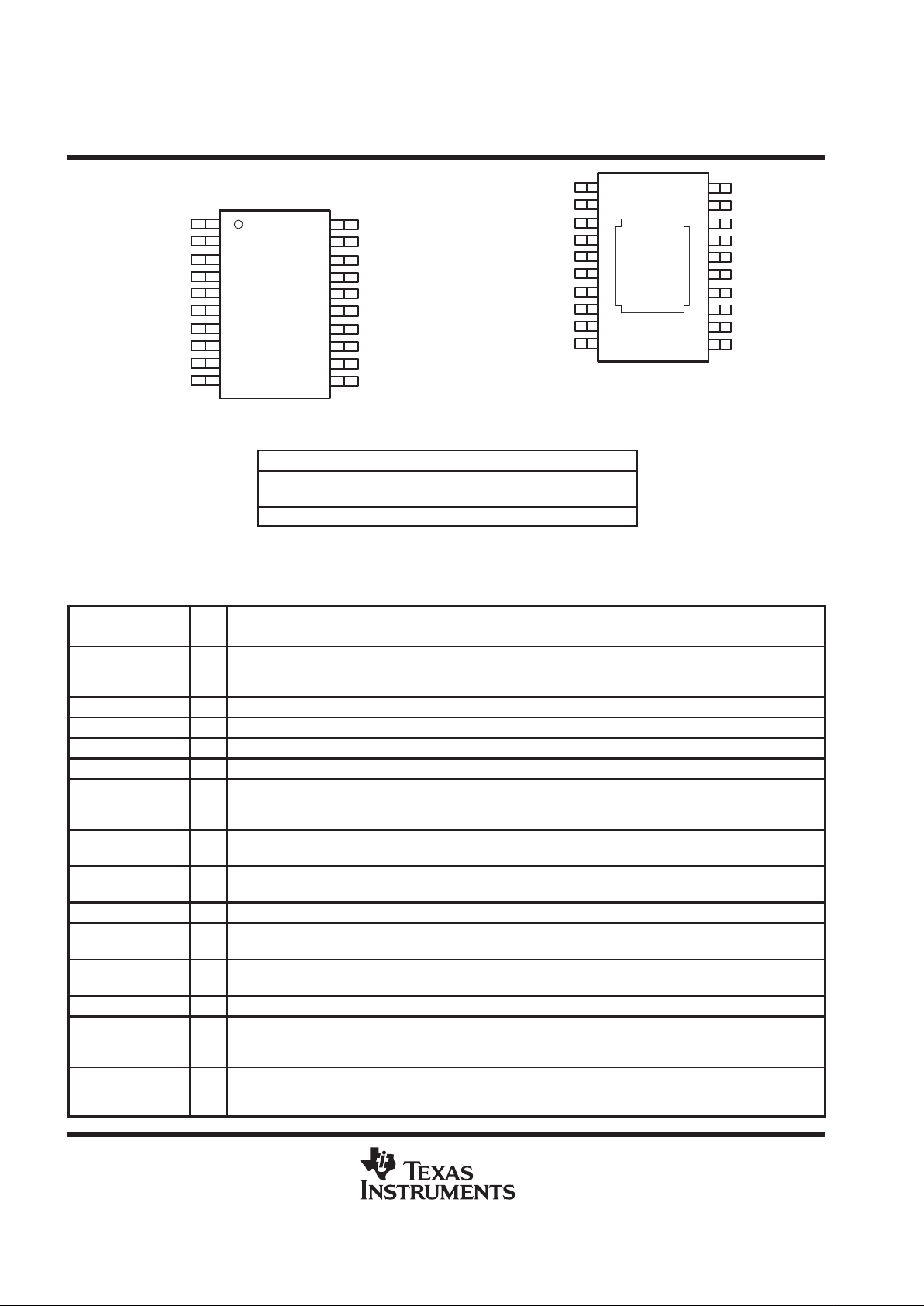
1
2
3
4
5
6
7
8
9
10
20
19
18
17
16
15
14
13
12
11
GND
SYNC
ENABLE
FB
OUT
C1+
IN
C1–
PGND
PGND
GND
3V8
COM
SKIP
OUT
C2+
IN
C2–
PGND
PGND
PWP PACKAGE
(TOP VIEW)
Figure 2. Bottom View of PWP Package,
Showing the Thermal Pad
Thermal
Pad
AVAILABLE OPTIONS
PACKAGE
TSSOP
†
(PWP)
TPS60100PWP
†
This package is available taped and reeled. To order this packaging
option, add an R suffix to the part number (e.g., TPS60100PWPR).
Terminal Functions
TERMINAL
NAME NO.
I/O
DESCRIPTION
3V8 19 I Mode selection.
When 3V8 is logic low the charge pump operates in the regulated 3.3-V mode. When 3V8 is connected to IN the
regulator operates in preregulated 3.8-V mode.
C1+ 6 Positive terminal of the charge-pump capacitor C
1F
C1– 8 Negative terminal of the charge-pump capacitor C
1F
C2+ 15 Positive terminal of the charge-pump capacitor C
2F
C2– 13 Negative terminal of the charge-pump capacitor C
2F
COM 18 I Mode selection.
When COM is logic low the charge pump operates in push-pull mode to minimize output ripple. When COM is
connected to IN the regulator operates in single-ended mode requiring only one flying capacitor.
ENABLE 3 I ENABLE Input. The device turns off, the output disconnects from the input, and the supply current decreases to
0.05 µA when ENABLE is a logic low. Connect ENABLE to IN for normal operation.
FB 4 I FEEDBACK input. Connect FB to OUT as close to the load as possible to achieve best regulation. Resistive divider
is on chip to match internal reference voltage of 1.22 V .
GND 1, 20 GROUND. Analog ground for internal reference and control circuitry. Connect to PGND through a short trace.
IN 7, 14 I Supply Input. Connect to an input supply in the 1.8-V to 3.6-V range. Bypass IN to GND with a (CO/2) µF capacitor.
Connect both INs through a short trace.
OUT 5, 16 O Regulated power output. Connect both OUT s through a short trace and bypass OUT to GND with the output filter
capacitor CO. VO = 3.3 V when 3V8 = low and VO = 3.8 V when 3V8 = high.
PGND 9–12 PGND power ground. Charge-pump current flows through this pin. Connect all PGNDs together.
SKIP 17 I Mode selection. When SKIP is logic low, the charge pump operates in constant-frequency mode. Output ripple
and noise are minimized in this mode. When SKIP is connect to IN, the device operates in pulse skip mode.
Quiescent current is lowest in this mode.
SYNC 2 I Selection for external clock signal. Connect to GND to use the internally generated clock signal. Connect to IN
for external synchronization. In this case, the clock signal needs to be fed through 3V8 and the device operates
in the regulated 3.3-V mode.
TPS60100
REGULATED 3.3 V 200-mA LOW-NOISE
CHARGE PUMP DC/DC CONVERTER
SLVS213B – MAY 1999 – REVISED SEPTEMBER 1999
3
POST OFFICE BOX 655303 • DALLAS, TEXAS 75265
absolute maximum ratings (unless otherwise noted)
†‡
Input voltage range, V
I
(IN, OUT, ENABLE, SKIP, COM, 3V8, FB, SYNC) –0.3 V to 5.5 V. . . . . . . . . . . . . . . .
Differential input voltage, V
ID
(C1+, C2+ to GND) –0.3 V to (V
OUT
+ 0.3 V). . . . . . . . . . . . . . . . . . . . . . . . . . . .
Differential input voltage, V
ID
(C1–, C2– to GND) –0.3 V to (VIN + 0.3 V). . . . . . . . . . . . . . . . . . . . . . . . . . . . . .
Continuous total power dissipation See Dissipation Rating Tables. . . . . . . . . . . . . . . . . . . . . . . . . . . . . . . . . . . .
Continuous output current 300 mA. . . . . . . . . . . . . . . . . . . . . . . . . . . . . . . . . . . . . . . . . . . . . . . . . . . . . . . . . . . . . . . .
Storage temperature range, T
stg
–55°C to 150°C. . . . . . . . . . . . . . . . . . . . . . . . . . . . . . . . . . . . . . . . . . . . . . . . . . .
Lead temperature 1,6 mm (1/16 inch) from case for 10s 260°C. . . . . . . . . . . . . . . . . . . . . . . . . . . . . . . . . . . . . . .
Maximum junction temperature, TJ 150°C. . . . . . . . . . . . . . . . . . . . . . . . . . . . . . . . . . . . . . . . . . . . . . . . . . . . . . . . .
†
Stresses beyond those listed under “absolute maximum ratings” may cause permanent damage to the device. These are stress ratings only, and
functional operation of the device at these or any other conditions beyond those indicated under “recommended operating conditions” is not
implied. Exposure to absolute-maximum-rated conditions for extended periods may affect device reliability.
‡
V
ENABLE
, V
SKIP
, V
COM
, V
3V8
and V
SYNC
can exceed VIN up to the maximum rated voltage without increasing the leakage current drawn by these
mode select inputs.
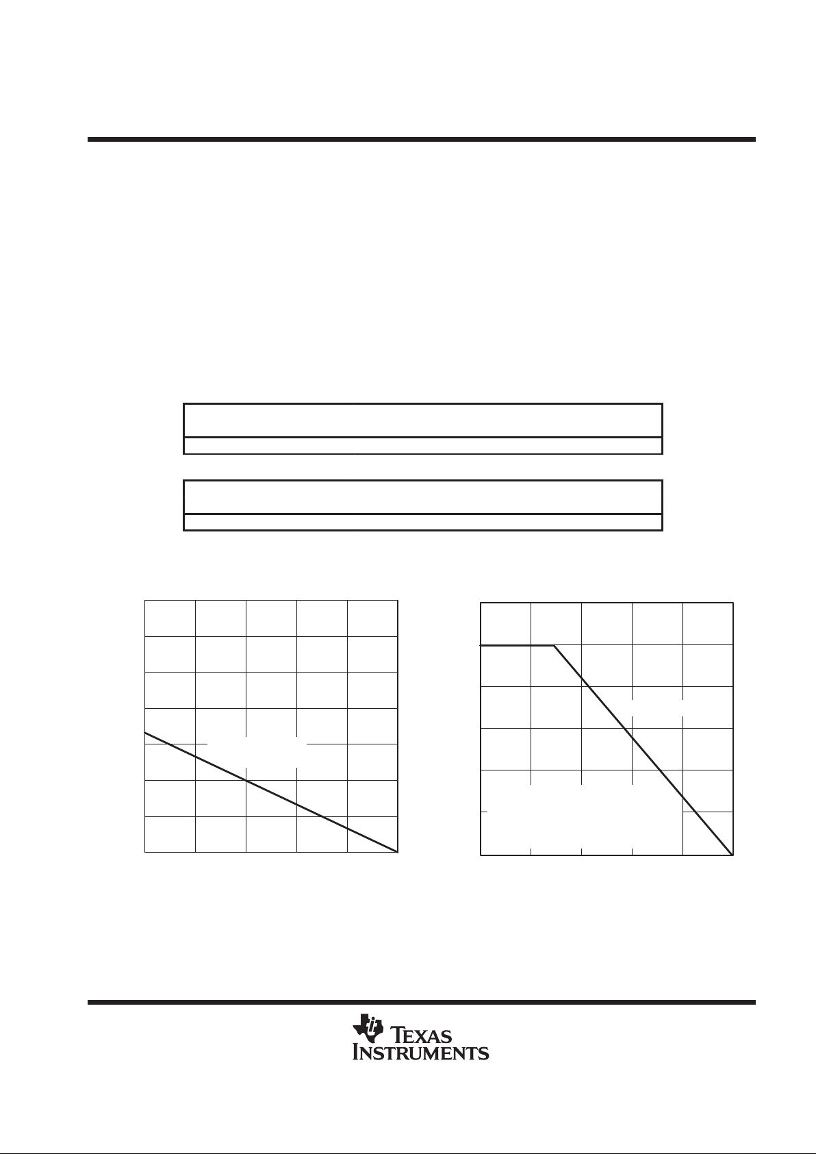
DISSIPATION RATING TABLE 1 – FREE-AIR TEMPERATURE (see Figure 3)
T
≤ 25°C DERATING FACTOR T
= 70°C T
= 85°C
PACKAGE
A
POWER RATING ABOVE TA = 25°CAPOWER RATINGAPOWER RATING
PWP 700 mW 5.6 mW/°C 448 mW 364 mW
DISSIPATION RATING TABLE 2 – CASE TEMPERATURE (see Figure 4)
T
≤ 62.5°C DERATING FACTOR T
= 70°C T
= 85°C
PACKAGE
C
POWER RATING ABOVE TC = 62.5°CCPOWER RATINGCPOWER RATING
PWP 25 W 285.7 mW/°C 22.9 W 18.5 W
Figure 3
1200
800
400
0
25 50 75 100
– Maximum Continuous Dissipation – mW
DISSIPATION DERATING CURVE
§
vs
FREE-AIR TEMPERATURE
125 150
1400
1000
600
200
PWP Package
R
θJA
= 178°C/W
P
D
TA – Free-Air Temperature – °C
Figure 4
MAXIMUM CONTINUOUS DISSIPATION
§
vs
CASE TEMPERATURE
TC – Case Temperature – °C
15
10
5
0
25 50 75 100
20
25
30
125 150
Measured with the exposed thermal pad
coupled to an infinite heat sink with a
thermally conductive compound (the
thermal conductivity of the compound
is 0.815 W/m ⋅°C). The R
θJC
is 3.5°C/W.
PWP Package
– Maximum Continuous Dissipation – W
P
D
§
Dissipation rating tables and figures are provided for maintenance of junction temperature at or below absolute maximum temperature of 150°C.
It is recommended not to exceed a junction temperature of 125°C.
TPS60100
REGULATED 3.3 V 200-mA LOW-NOISE
CHARGE PUMP DC/DC CONVERTER
SLVS213B – MAY 1999 – REVISED SEPTEMBER 1999
4
POST OFFICE BOX 655303 • DALLAS, TEXAS 75265
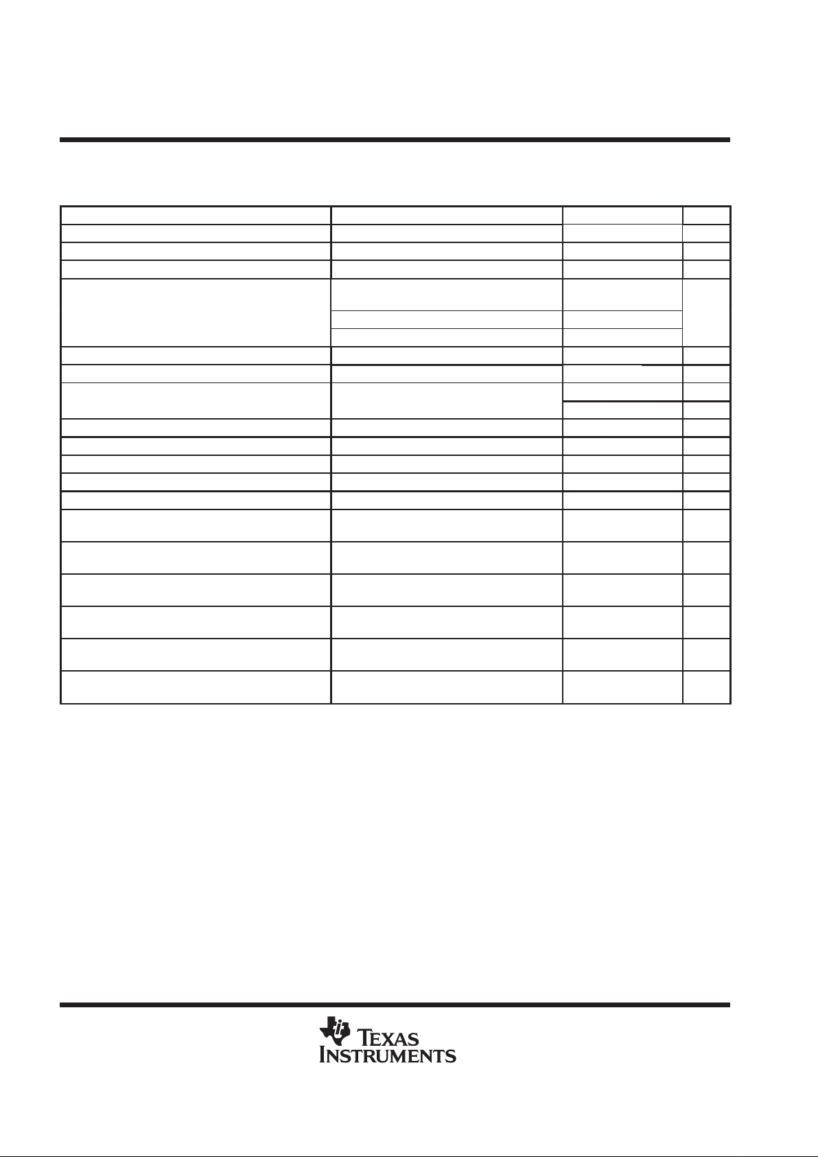
electrical characteristics at CIN = 10 µF, C1F = C2F = 2.2 µF†, CO = 22 µF, TC = –40°C to 85°C,
V
IN
= 2 V, VFB = VO, V
ENABLE
= VIN, V
SKIP
= VIN or 0 V and V
COM
= V
3V8
= V
SYNC
= 0 V (unless otherwise
noted)
PARAMETER TEST CONDITIONS MIN TYP MAX UNIT
V
IN
Input voltage
1.8 3.6 V
V
IN(UV)
Input undervoltage lockout threshold 1.6 1.8 V
I
O(MAX)
Maximum output current 200 mA
1.8 V < VIN < 2 V, 0 < IO < 100 mA,
V
O(Start-Up)
= 3.3 V, TC = 25°C
3.17 3.3 3.43
V
O
Output voltage
2 V < VIN < 3.3 V, 0 < IO < 200 mA
3.17 3.3 3.43
V
3.3 V < VIN < 3.6 V, 0 < IO < 200 mA 3.17 3.3 3.47
V
O(RIP)
Output voltage ripple IO = 200 mA, V
SKIP
= 0 V 5
‡
mV
PP
I
O(LEAK)
Output leakage current VIN = 2.4 V, V
ENABLE
= 0 V 1 µA
Quiescent current V
= V
= 2.4 V
50 90 µA
I
Q
(no-load input current)
SKIP IN
V
SKIP
= 0 V, VIN = 2.4 V
1.5 mA
I
DD(SDN)
Shutdown supply current VIN = 2.4 V, V
ENABLE
= 0 V 0.05 1 µA
f
OSC(int)
Internal switching frequency VIN = 2.4 V 200 300 400 kHz
f
OSC(ext)
External clock frequency V
SYNC
= VIN,V
IN
= 1.8V to 3.6 V 400 600 800 kHz
External clock duty cycle V
SYNC
= VIN,V
IN
= 1.8V to 3.6 V 20% 80%
Efficiency IO = 100 mA 80%
V
INL
Input voltage low,
ENABLE, SKIP, COM, 3V8, SYNC
VIN = 1.8 V
0.3 ×
V
IN
V
V
INH
Input voltage high,
ENABLE, SKIP, COM, 3V8, SYNC
VIN = 3.6 V
0.7 ×
V
IN
V
I
I(LEAK)
Input leakage current,
ENABLE, SKIP, COM, 3V8, SYNC
V
ENABLE
= V
SKIP
= V
COM
= V
3V8
=
V
SYNC
= V
GND
or V
IN
0.01 0.1 µA
Output load regulation
VO = 3.3 V, 1 mA < IO < 200 mA
TC = 25°C
0.004 %/mA
Output line regulation
2 V < VIN < 3.3 V, VO = 3.3 V,
IO = 100 mA, TC = 25°C
0.6 %/V
Short circuit current
VIN = 2.4 V VO = 0 V,
TC = 25°C
125 mA
†
Use only ceramic capacitors with X5R or X7R dielectric as flying capacitors.
‡
Achieved with CO = 22 µF X5R dielectric ceramic capacitor
TPS60100
REGULATED 3.3 V 200-mA LOW-NOISE
CHARGE PUMP DC/DC CONVERTER
SLVS213B – MAY 1999 – REVISED SEPTEMBER 1999
5
POST OFFICE BOX 655303 • DALLAS, TEXAS 75265
electrical characteristics for preregulated 3.8-V Mode (V
(3V8)
= VIN), CIN = 10 µF,
C
1F
= C2F = 2.2 µF†, CO = 22 µF, TC = –40°C to 85°C, VIN = 2.4 V, VFB = VO, V
ENABLE
= VIN,
V
SKIP
= VIN or 0 V and V
COM
= V
SYNC
= 0 V (unless otherwise noted)
PARAMETER TEST CONDITIONS MIN TYP MAX UNIT
V
IN
Input voltage 2.2 3.6 V
I
O(MAX)
Maximum output current 200 mA
V
O
Output voltage 2.2 V < VIN < 3.6 V, 0 < IO < 200 mA 3.6 3.8 4 V
I
O(LEAK)
Output leakage current V
ENABLE
= 0 V 1 µA
Quiescent current
V
SKIP
= V
IN
60 µA
I
Q
(no-load input current)
V
SKIP
= 0 V
2 mA
I
DD(SDN)
Shutdown supply current V
ENABLE
= 0 V 0.05 1 µA
f
OSC
Internal switching frequency 200 300 400 kHz
Short circuit current VO = 0 V, TC = 25°C 125 mA
†
Use only ceramic capacitors with X5R or X7R dielectric as flying capacitors.
TPS60100
REGULATED 3.3 V 200-mA LOW-NOISE
CHARGE PUMP DC/DC CONVERTER
SLVS213B – MAY 1999 – REVISED SEPTEMBER 1999
6
POST OFFICE BOX 655303 • DALLAS, TEXAS 75265
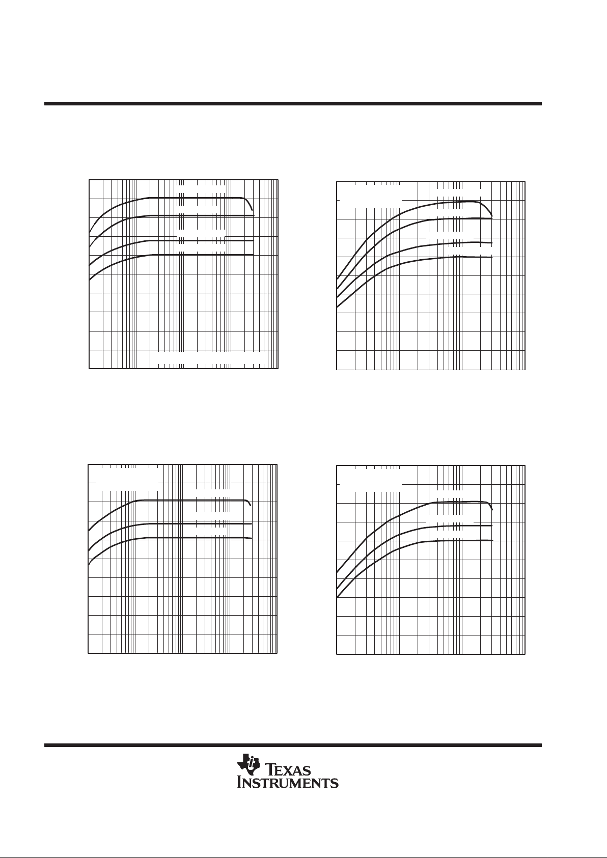
TYPICAL CHARACTERISTICS
†
Figure 5
50
40
20
0
0.1 1 10
Efficiency – %
70
90
EFFICIENCY
vs
OUTPUT CURRENT (V
O
= 3.3 V)
100
100 1000
80
60
30
10
IO – Output Current – mA
V
(SKIP)
= VIN, V
(3V8)
= 0 V
VIN = 1.8 V
VIN = 2 V
VIN = 2.4 V
VIN = 2.7 V
Figure 6
50
40
20
0
110
Efficiency – %
70
90
EFFICIENCY
vs
OUTPUT CURRENT (V
O
= 3.3 V)
100
100 1000
80
60
30
10
IO – Output Current – mA
V
(SKIP)
= 0 V
V
(3V8)
= 0 V
VIN = 1.8 V
VIN = 2 V
VIN = 2.4 V
VIN = 2.7 V
Figure 7
50
40
20
0
0.1 1 10
Efficiency – %
70
90
EFFICIENCY
vs
OUTPUT CURRENT (V
O
= 3.8 V)
100
100 1000
80
60
30
10
IO – Output Current – mA
V
(SKIP)
= V
IN
V
(3V8)
= V
IN
VIN = 3 V
VIN = 2.3 V
VIN = 2.7 V
Figure 8
50
40
20
0
110
Efficiency – %
70
90
EFFICIENCY
vs
OUTPUT CURRENT (V
O
= 3.8 V)
100
100 1000
80
60
30
10
IO – Output Current – mA
V
(SKIP)
= 0 V
V
(3V8)
= V
IN
VIN = 3 V
VIN = 2.3 V
VIN = 2.7 V
†TC = 25°C, V
COM
= V
SYNC
= 0 V, CIN = 10 µF, C1F = C2F = 2.2 µF, CO = 22 µF, unless otherwise noted
TPS60100
REGULATED 3.3 V 200-mA LOW-NOISE
CHARGE PUMP DC/DC CONVERTER
SLVS213B – MAY 1999 – REVISED SEPTEMBER 1999
7
POST OFFICE BOX 655303 • DALLAS, TEXAS 75265
TYPICAL CHARACTERISTICS
†
Figure 9
40
35
30
25
1.5 2 2.5 3
– Quiescent Supply Current –
50
55
QUIESCENT SUPPLY CURRENT
vs
INPUT VOLTAGE
60
3.5 4
45
VIN – Input Voltage – V
I
Q
Aµ
V
(SKIP)
= V
IN
V
(3V8)
= 0 V
Figure 10
1.5
1.25
1
1.5 2 2.5 3
1.75
2
3.5 4
– Quiescent Supply Current – mA
QUIESCENT SUPPLY CURRENT
vs
INPUT VOLTAGE
VIN – Input Voltage – V
I
Q
V
(SKIP)
= 0 V
V
(3V8)
= 0 V
Figure 11
IO – Output Current – mA
3.3
3.2
3.1
3
110
– Output Voltage – V
3.4
3.5
OUTPUT VOLTAGE
vs
OUTPUT CURRENT
3.6
100 1000
V
O
V
(SKIP)
= VIN or 0 V
V
(3V8)
= 0 V
VIN = 2.7 V
VIN = 2.4 V
VIN = 2 V
VIN = 1.8 V
VIN = 3.6 V
Figure 12
IO – Output Current – mA
3.8
3.7
3.6
3.5
110
– Output Voltage – V
3.9
4
OUTPUT VOLTAGE
vs
OUTPUT CURRENT
4.1
100 1000
V
O
V
(SKIP)
= VIN or 0 V
V
(3V8)
= V
IN
VIN = 3.6 V
VIN = 2.7 V
VIN = 2.4 V
†TC = 25°C, V
COM
= V
SYNC
= 0 V, CIN = 10 µF, C1F = C2F = 2.2 µF, CO = 22 µF, unless otherwise noted

TPS60100
REGULATED 3.3 V 200-mA LOW-NOISE
CHARGE PUMP DC/DC CONVERTER
SLVS213B – MAY 1999 – REVISED SEPTEMBER 1999
8
POST OFFICE BOX 655303 • DALLAS, TEXAS 75265
TYPICAL CHARACTERISTICS
†
Figure 13
3.35
3.2
3.1
3
1.5 2 2.5 3
– Output Voltage – V
3.4
3.45
OUTPUT VOLTAGE
vs
INPUT VOLTAGE
3.5
3.5 4
3.3
3.25
3.15
3.05
VIN – Input Voltage – V
V
O
V
(SKIP)
= VIN or 0 V
V
(3V8)
= 0 V
IO = 1 mA to 200 mA
Figure 14
3.7
3.4
3.2
3
1.5 2 2.5 3
– Output Voltage – V
3.8
3.9
OUTPUT VOLTAGE
vs
INPUT VOLTAGE
3.10
3.5 4
3.6
3.5
3.3
3.1
VIN – Input Voltage – V
V
O
V
(SKIP)
= VIN or 0 V
V
(3V8)
= V
IN
IO = 10 mA
IO = 100 mA
IO = 200 mA
Figure 15
3.33
3.32
3.31
3.30
012345
3.34
3.35
OUTPUT VOLTAGE
vs
TIME
3.36
678
t – Time – µs
V
(SKIP)
= 0 V
V
(3V8)
= 0 V
VIN = 2.4 V
IO = 100 mA
CO = 22 µF (X5R ceramic)
Constant
Frequency
Mode
Less than
5 mVpp
– Output Voltage – V
V
O
Figure 16
3.34
3.32
3.3
02 4 6 81012
3.36
OUTPUT VOLTAGE
vs
TIME
3.38
14 16 18 20
t – Time – µs
V
(SKIP)
= V
IN
V
(3V8)
= 0 V
VIN = 2.4 V
IO = 200 mA
Pulse-Skip Mode
– Output Voltage – V
V
O
†TC = 25°C, V
COM
= V
SYNC
= 0 V, CIN = 10 µF, C1F = C2F = 2.2 µF, CO = 22 µF, unless otherwise noted

TPS60100
REGULATED 3.3 V 200-mA LOW-NOISE
CHARGE PUMP DC/DC CONVERTER
SLVS213B – MAY 1999 – REVISED SEPTEMBER 1999
9
POST OFFICE BOX 655303 • DALLAS, TEXAS 75265
TYPICAL CHARACTERISTICS
†
Figure 17
3.32
400
200
0
0 2 4 6 8 10 12
– Output Voltage – V
3.33
3.35
t – Time – ms
LOAD TRANSIENT RESPONSE
3.36
14 16 18 20
600
3.34
V
O
– Output Current – mA
I
O
V
(SKIP)
= 0 V
V
(3V8)
= 0 V
V
(IN)
= 2.7 V
IO = 10 mA to 200 mA
Constant
Frequency
Mode
Figure 18
3.31
400
200
0
0 2 4 6 8 10 12
3.33
3.37
t – Time – ms
LOAD TRANSIENT RESPONSE
3.39
14 16 18 20
600
3.35
V
(SKIP)
= V
IN
V
(3V8)
= 0 V
V
(IN)
= 2.7 V
IO = 10 mA to 200 mA
Pulse-Skip Mode
– Output Voltage – V
V
O
– Output Current – mA
I
O
Figure 19
3.31
2.5
2
1.5
0123456
– Output Voltage – V
3.33
3.37
t – Time – ms
LINE TRANSIENT RESPONSE
3.39
78 910
3
3.35
V
O
– Input Voltage – V
V
IN
V
(SKIP)
= 0 V
V
(3V8)
= 0 V
IO = 100 mA
Constant
Frequency
Mode
Figure 20
3.25
2.5
2
1.5
0123456
3.3
3.4
t – Time – ms
LINE TRANSIENT RESPONSE
3.45
78 910
3
3.35
V
(SKIP)
= V
IN
V
(3V8)
= 0 V
IO = 100 mA
Pulse-Skip Mode
– Output Voltage – V
V
O
– Input Voltage – V
V
IN
†TC = 25°C, V
COM
= V
SYNC
= 0 V, CIN = 10 µF, C1F = C2F = 2.2 µF, CO = 22 µF, unless otherwise noted

TPS60100
REGULATED 3.3 V 200-mA LOW-NOISE
CHARGE PUMP DC/DC CONVERTER
SLVS213B – MAY 1999 – REVISED SEPTEMBER 1999
10
POST OFFICE BOX 655303 • DALLAS, TEXAS 75265
TYPICAL CHARACTERISTICS
†
Figure 21
50
40
20
0
0 2.5 5
Output – dB
60
80
f – Frequency – MHz
FREQUENCY SPECTRUM
CONSTANT FREQUENCY MODE
‡
90
7.5 10
70
30
10
Vµ
V
(SKIP)
= 0 V
V
(3V8)
= 0 V
VIN = 2.4 V
IO = 100 mA
RBW = 300 Hz
Figure 22
40
20
0
0 2.5 5
Output – dB
60
100
f – Frequency – MHz
FREQUENCY SPECTRUM
PULSE-SKIP MODE
‡
7.5 10
Vµ
V
(SKIP)
= V
IN
V
(3V8)
= 0 V
VIN = 2.4 V
IO = 100 mA
RBW = 300 Hz
80
Figure 23
50
20
10
0
0 2.5 5
60
70
f – Frequency – MHz
FREQUENCY SPECTRUM
CONSTANT FREQUENCY MODE
‡
90
7.5 10
30
40
80
Output – dB Vµ
V
(SKIP)
= 0 V
V
(3V8)
= 0 V
VIN = 2.4 V
IO = 10 mA
RBW = 300 Hz
Figure 24
50
40
20
0
0 2.5 5
Output – dB
60
80
f – Frequency – MHz
FREQUENCY SPECTRUM
PULSE-SKIP MODE
‡
90
7.5 10
70
30
10
Vµ
V
(SKIP)
= V
IN
V
(3V8)
= 0 V
VIN = 2.4 V
IO = 10 mA
RBW = 300 Hz
†TC = 25°C, V
COM
= V
SYNC
= 0 V, CIN = 10 µF, C1F = C2F = 2.2 µF, CO = 22 µF, unless otherwise noted
‡Test circuit: TPS60100EVM–131

TPS60100
REGULATED 3.3 V 200-mA LOW-NOISE
CHARGE PUMP DC/DC CONVERTER
SLVS213B – MAY 1999 – REVISED SEPTEMBER 1999
11
POST OFFICE BOX 655303 • DALLAS, TEXAS 75265
TYPICAL CHARACTERISTICS
†
Figure 25
Skip = High
Skip = Low
V
(3V8)
= 0 V
IO = 100 mA
50
30
20
0
1.5 2 2.5 3
Efficiency – %
70
80
EFFICIENCY
vs
INPUT VOLTAGE
100
3.5 4
10
40
60
90
VIN – Input Voltage – V
Figure 26
Skip = High
Skip = Low
V
(3V8)
= V
IN
IO = 100 mA
50
30
20
0
1.5 2 2.5 3
Efficiency – %
70
80
EFFICIENCY
vs
INPUT VOLTAGE
100
3.5 4
10
40
60
90
VIN – Input Voltage – V
Figure 27
t – Time –µs
2
1.5
1
0.5
–100 0
– Output Voltage – V
2.5
3
START-UP TIMING
3.5
100 200
V
O
R0 = 16.5 Ω
VIN = 2.4 V
V
(3V8)
= 0 V
Enable
OUTPUT
0
–0.5
300 400 500 600
Figure 28
t – Time –µs
2.5
2
1.5
1
–100 0
– Output Voltage – V
3
3.5
START-UP TIMING
4
100 200
V
O
0.5
–0.5
300 400 500 600
0
Enable
OUTPUT
R0 = 19 Ω
VIN = 2.4 V
V
(3V8)
= V
IN
†TC = 25°C, V
COM
= V
SYNC
= 0 V, CIN = 10 µF, C1F = C2F = 2.2 µF, CO = 22 µF, unless otherwise noted

TPS60100
REGULATED 3.3 V 200-mA LOW-NOISE
CHARGE PUMP DC/DC CONVERTER
SLVS213B – MAY 1999 – REVISED SEPTEMBER 1999
12
POST OFFICE BOX 655303 • DALLAS, TEXAS 75265
detailed description
operating principle
The TPS60100 charge pump provides a regulated 3.3-V output from a 1.8-V to 3.6-V input. It delivers a
maximum load current of 200 mA. Designed specifically for space critical battery powered applications, the
complete charge pump circuit requires only four external capacitors. The circuit can be optimized for highest
efficiency at light loads or lowest output noise. The TPS60100 consists of an oscillator, a 1.22-V bandgap
reference, an internal resistive feedback circuit, an error amplifier, high current MOSFET switches, a
shutdown/start-up circuit, and a control circuit (Figure 29)
C1+
C1–
ENABLE
OUT
FB
0°
180°
PGND
C
1F
IN
CHARGE PUMP 2
C2+
C2–
OUT
PGND
C
2F
IN
T
22
T
21
OSCILLATOR
GND
SKIP
COM
3V8
V
REF
–
+
–
+
CONTROL
CIRCUIT
0.8 × V
IN
–
+
–
+
SHUTDOWN/
START-UP
CONTROL
SYNC
T
11
T
12
T
13
T
14
T
24
T
23
CHARGE PUMP 1
Figure 29. Functional Block Diagram TPS60100
The oscillator runs at a 50% duty cycle. The device consists of two single-ended charge pumps which operate
with 180° phase shift. Each single ended charge pump transfers charge into its transfer capacitor (CxF) in one
half of the period. During the other half of the period (transfer phase), CxF is placed in series with the input to
transfer its charge to C
O
. While one single-ended charge pump is in the charge phase, the other one is in the
transfer phase. This operation guarantees an almost constant output current which ensures a low output ripple.
If the clock were to run continuously , this process would eventually generate an output voltage equal to two times
the input voltage (hence the name doubler). In order to provide a regulated fixed output voltage of 3.3 V, the
TPS60100 uses either pulse-skip mode or constant-frequency mode. Pulse-skip mode and constant-frequency
mode are externally selected via the SKIP input pin.

TPS60100
REGULATED 3.3 V 200-mA LOW-NOISE
CHARGE PUMP DC/DC CONVERTER
SLVS213B – MAY 1999 – REVISED SEPTEMBER 1999
13
POST OFFICE BOX 655303 • DALLAS, TEXAS 75265
detailed description (continued)
start-up procedure
During start-up, i.e. when ENABLE is set from logic low to logic high, the switches T12 and T14 (charge pump
1), and the switches T22 and T24 (charge pump 2) are conducting to charge up the output capacitor until the
output voltage VO reaches 0.8×VIN. When the start-up comparator detects this limit, the IC begins to operate
in the mode selected with SKIP , COM and 3V8. This start-up charging of the output capacitor guarantees a short
start-up time and eliminates the need for a Schottky diode between IN and OUT.
pulse-skip mode
In pulse-skip mode (SKIP = high), the error amplifier disables switching of the power stages when it detects an
output higher than 3.3 V . The oscillator halts. The IC then skips switching cycles until the output voltage drops
below 3.3 V . Then the error amplifier reactivates the oscillator and switching of the power stages starts again.
The pulse-skip regulation mode minimizes operating current because it does not switch continuously and
deactivates all functions except bandgap reference and error amplifier when the output is higher than 3.3 V.
When switching is disabled from the error amplifier, the load is also isolated from the input. SKIP is a logic input
and should not remain floating. The typical operating circuit of the TPS60100 in pulse skip mode is shown in
Figure 1.
constant-frequency mode
When SKIP is low, the charge pump runs continuously at the frequency f
OSC
. The control circuit, fed from the
error amplifier, controls the charge on C1F and C2F by driving the gates of the FETs T12/T13 and T22/T23,
respectively. When the output voltage falls, the gate drive increases, resulting in a larger voltage across C
1F
and C2F. This regulation scheme minimizes output ripple. Since the device switches continuously, the output
noise contains well-defined frequency components, and the circuit requires smaller external capacitors for a
given output ripple. However, constant-frequency mode, due to higher operating current, is less ef ficient at light
loads than pulse-skip mode.
IN
IN
C1+
C1–
ENABLE
OUT
OUT
FB
C2+
C2–
SYNC
SKIP COM 3V8
PGND GND
INPUT
1.8 V to 3.6 V
CIN
10 µF
OUTPUT
3.3 V 200 mA
CO = 22 µF
C
2F
2.2 µF
C
1F
2.2 µF
+
OFF/ON
TPS60100
+
Figure 30. Typical Operating Circuit TPS60100 in Constant Frequency Mode
Table 1. Tradeoffs Between Operating Modes
FEATURE PULSE-SKIP MODE
(SKIP = High)
CONSTANT-FREQUENCY MODE
(SKIP = Low)
Best light-load efficiency X
Smallest external component size for a given output ripple X
Output ripple amplitude Small amplitude Very small amplitude
Output ripple frequency Variable Constant
Load regulation Very good Good
NOTE: Even in pulse-skip mode the output ripple amplitude is small if the push-pull operating mode is selected via COM.

TPS60100
REGULATED 3.3 V 200-mA LOW-NOISE
CHARGE PUMP DC/DC CONVERTER
SLVS213B – MAY 1999 – REVISED SEPTEMBER 1999
14
POST OFFICE BOX 655303 • DALLAS, TEXAS 75265
detailed description (continued)
push-pull operating mode
In push-pull operating mode (COM = low), the two single-ended charge pumps operate with 180° phase shift.
The oscillator signal has a 50% duty cycle. Each single-ended charge pump transfers charge into its transfer
capacitor (CxF) in one-half of the period. During the other half of the period (transfer phase), CxF is placed in
series with the input to transfer its charge to C
O
. While one single-ended charge pump is in the charge phase,
the other one is in the transfer phase. This operation guarantees an almost constant output current which
ensures a low output ripple. COM is a logic input and should not remain floating. The typical operating circuit
of the TPS60100 in push-pull mode is shown in Figure 1 and Figure 30.
single-ended operating mode
When COM is high, the device runs in single-ended operating mode. The two single-ended charge pumps
operate in parallel without phase shift. They transfer charge into the transfer capacitor (CF) in one half of the
period. During the other half of the period (transfer phase), CF is placed in series with the input to transfer its
charge to CO. In single-ended operating mode only one transfer capacitor (CF = C1F + C2F) is required, resulting
in less board space.
IN
IN
C1+
C1–
ENABLE
OUT
OUT
FB
C2+
C2–
SYNC
SKIP COM 3V8
PGND GND
INPUT
1.8 V to 3.6 V
CIN
10 µF
OUTPUT
3.3 V 200 mA
CO = 22 µF
CF = 4.7 µF
+
OFF/ON
TPS60100
+
Figure 31. Typical Operating Circuit TPS60100 in Single-Ended Operating Mode
Table 2. Tradeoffs Between Operating Modes
FEATURE PUSH-PULL MODE
(COM = Low)
SINGLE-ENDED MODE
(COM = High)
Output ripple amplitude Small amplitude Large amplitude
Smallest board space X
regulated 3.3 V operating mode
In regulated 3.3 V operating mode (3V8 = low) the device provides a regulated 3.3-V output from a1.8-V to 3.6-V
input. 3V8 is a logic input and should not remain floating. The typical operating circuit of the TPS60100 in (3.3
V) regulated mode is shown in Figure 1 and Figure 30.
pre-regulated 3.8 V operating mode
When 3V8 is high, the device provides a preregulated 3.8-V output from a 2.2-V to 3.6-V input. This mode should
be used if a tighter output voltage tolerance is a major concern. In this case the charge pump generates the input
voltage for a low-dropout regulator.

TPS60100
REGULATED 3.3 V 200-mA LOW-NOISE
CHARGE PUMP DC/DC CONVERTER
SLVS213B – MAY 1999 – REVISED SEPTEMBER 1999
15
POST OFFICE BOX 655303 • DALLAS, TEXAS 75265
detailed description (continued)
shutdown
Driving ENABLE low places the device in shutdown mode. This disables all switches, the oscillator, and control
logic. The device typically draws 0.05-µA (1-µA max) of supply current in this mode. Leakage current drawn from
the output is as low as 1 µA max. The device exits shutdown once ENABLE is set high level. The typical no-load
shutdown exit time is 10 µs. When the device is in shutdown, the load is isolated from the input and the output
is high impedance.
external clock signal
If the device shall operate at a user defined frequency , an external clock signal can be used. Therefore, SYNC
needs to be connected to IN and the external oscillator signal can drive 3V8. The maximum external frequency
is limited to 800 kHz. The switching frequency of the converter is half of the external oscillator frequency . It is
recommended to operate the charge pump in constant-frequency mode if an external clock signal is used so
that the output noise contains only well-defined frequency components.
IN
IN
C1+
C1–
ENABLE
OUT
OUT
FB
C2+
C2–
SYNC
SKIP COM 3V8
PGND GND
INPUT
1.8 V to 3.6 V
CIN
10 µF
OUTPUT
3.3 V 200 mA
CO = 22 µF
C
2F
2.2 µF
C
1F
2.2 µF
+
OFF/ON
TPS60100
+
External Clock
Figure 32. Typical Operating Circuit TPS60100 With External Synchronization
undervoltage lockout
The TPS60100 has an undervoltage lockout feature that deactivates the device and places it in shutdown mode
when the input voltage falls below 1.6 V.

TPS60100
REGULATED 3.3 V 200-mA LOW-NOISE
CHARGE PUMP DC/DC CONVERTER
SLVS213B – MAY 1999 – REVISED SEPTEMBER 1999
16
POST OFFICE BOX 655303 • DALLAS, TEXAS 75265
APPLICATION INFORMATION
capacitor selection
The TPS60100 requires only four external capacitors as shown in the basic application circuit. Their values are
closely linked to the output current capacity , output noise requirements, and mode of operation. Generally , the
transfer capacitors (CxF) will be the smallest.
The input capacitor improves system efficiency by reducing the input impedance and stabilizes the input current.
CIN is recommended to be about two to four times as large as CxF.
The output capacitor (CO) can be selected from 5-times to 50-times larger than CxF, depending on the mode
of operation and ripple tolerance†. Tables 3 and 4 show capacitor values recommended for low
quiescent-current operation (pulse-skip mode) and for low output voltage ripple operation (constant-frequency
mode). A recommendation is given for smallest size.
Table 3. Recommended Capacitor Values for Low Quiescent-Current Operation
†
(pulse-skip mode)
VIN
I
[mA]
C
IN
[µF]
CxF
C
O
[µF]
OUTPUT
VOLTAGE
[V]
O
[]
TANTALUM CERAMIC
[µF]
TANTALUM CERAMIC
RIPPLE V
PP
[mV]
2.4 150 10 2.2 22 90
2.4 150 10 (X5R) 2.2 22 (X5R) 45
2.4 200 10 2.2 22 55
2.4 200 10 (X5R) 2.2 22 (X5R) 30
†
All measurements are done with additional 1-µF X7R ceramic capacitors at input and output.
Table 4. Recommended Capacitor Values for Low Output Voltage Ripple Operation
†
(constant-frequency mode)
VIN
I
O
C
IN
[µF]
CxF
C
O
[µF]
OUTPUT
VOLTAGE
[V]
[mA]
TANTALUM CERAMIC
[µF]
TANTALUM CERAMIC
RIPPLE V
PP
[mV]
2.4 150 10 2.2 22 13
2.4 150 10 (X5R) 2.2 22 (X5R) 4
2.4 200 10 2.2 22 15
2.4 200 10 (X5R) 2.2 22 (X5R) 5
†
All measurements are done with additional 1-µF X7R ceramic capacitors at input and output.
†
In constant-frequency mode always select CO ≥ 22 µF

TPS60100
REGULATED 3.3 V 200-mA LOW-NOISE
CHARGE PUMP DC/DC CONVERTER
SLVS213B – MAY 1999 – REVISED SEPTEMBER 1999
17
POST OFFICE BOX 655303 • DALLAS, TEXAS 75265
APPLICATION INFORMATION
For the TPS60100, the smallest board space size can be achieved using Sprague’s 595D-series tantalum
capacitors for input and output. However, with the trend towards high capacitance ceramic capacitors in smaller
size packages, these type of capacitors might become competitive in size soon.
Table 5. Recommended Capacitors
MANUFACTURER PART NUMBER CAPACITANCE TYPE
Taiyo Yuden LMK212BJ105KG–T
LMK212BJ225MG–T
JMK316BJ106ML–T
LMK432BJ226MM–T
1 µF
2.2 µF
10 µF
22 µF
Ceramic
Ceramic
Ceramic
Ceramic
AVX 0805ZC105KAT2A
1206ZC225KAT2A
TPSC106025R0500
TPSC226016R0375
1 µF
2.2 µF
10 µF
22 µF
Ceramic
Ceramic
Tantalum
Tantalum
Sprague 595D106X0010A2T
595D226X06R3A2T
595D226X06R3B2T
595D226X0020C2T
10 µF
22 µF
22 µF
22 µF
Tantalum
Tantalum
Tantalum
Tantalum
Kemet T494C106M010AS
T494C226M010AS
10 µF
22 µF
Tantalum
Tantalum
Table 6 lists the manufacturers of recommended capacitors. In most applications surface-mount tantalum
capacitors will be the right choice. However, ceramic capacitors will provide the lowest output voltage ripple due
to their typically lower ESR.
Table 6. Recommended Capacitor Manufacturers
MANUFACTURER CAPACITOR TYPE INTERNET
Taiyo Yuden X7R/X5R ceramic www.t–yuden.com
AVX X7R/X5R ceramic
TPS–series tantalum
www.avxcorp.com
Sprague 595D–series tantalum
593D–series tantalum
www.vishay.com
Kemet T494–series tantalum www.kemet.com
power dissipation
The power dissipated in the TPS60100 depends on output current and is approximated by:
P
DISS
+
IO ǒ2VIN*
V
O
Ǔ
for IQtt
I
O
P
DISS
must be less than that allowed by the package rating. See the ratings for 20-PowerPAD package
power-dissipation limits and deratings.

TPS60100
REGULATED 3.3 V 200-mA LOW-NOISE
CHARGE PUMP DC/DC CONVERTER
SLVS213B – MAY 1999 – REVISED SEPTEMBER 1999
18
POST OFFICE BOX 655303 • DALLAS, TEXAS 75265
APPLICATION INFORMATION
layout
All capacitors should be soldered in close proximity to the IC. A PCB layout proposal for a two-layer board is
given in Figure 33. Care has been taken to connect both single-ended charge pumps symmetrically to the load
to achive optimized output voltage ripple performance. The proposed layout also provides improved thermal
performance as the exposed leadframe is soldered to the PCB. The bottom layer of the PCB is a ground plain
only . All ground areas on the PCB should be connected. Connect ground areas on top layer to the bottom layer
via through hole connections.
GND
GND
GND
ENABLE
SYNC
C1+
C1–
GND
GND
OUT
IN
3V8
COM
SKIP
C2+
C2–
Figure 33. Recommended PCB Layout for TPS60100 (top view)
An evaluation module for the TPS60100 is available and can be ordered under literature code SL VP131 or under
product code TPS60100EVM–131.

TPS60100
REGULATED 3.3 V 200-mA LOW-NOISE
CHARGE PUMP DC/DC CONVERTER
SLVS213B – MAY 1999 – REVISED SEPTEMBER 1999
19
POST OFFICE BOX 655303 • DALLAS, TEXAS 75265
APPLICATION INFORMATION
applications proposals
paralleling of two TPS60100 to deliver 400 mA
The TPS60100 can be paralleled to yield higher load currents. The circuit of Figure 34 can deliver 400 mA at
an output voltage of 3.3 V. It uses two TPS60100 devices in parallel. The devices can share the output
capacitors, but each one requires its own transfer capacitors and input capacitor. For best performance, the
paralleled devices should operate in the same mode (pulse-skip or constant frequency).
IN
IN
C1+
C1–
ENABLE
OUT
OUT
FB
C2+
C2–
SYNC
SKIP COM 3V8
PGND GND
INPUT
1.8 V to
3.6 V
10 µF
2.2 µF
2.2 µF
+
OFF/ON
TPS60100
IN
IN
C1+
C1–
ENABLE
OUT
OUT
FB
C2+
C2–
SYNC
SKIP COM 3V8
PGND GND
10 µF
OUTPUT
3.3 V
200 mA
47 µF
2.2 µF2.2 µF
+
TPS60100
+
Figure 34. Paralleling of Two TPS60100
TPS60100 with LC output filter for ultra low ripple
For applications where extremely low output ripple is required, a small LC filter is recommended. This is shown
in Figure 35. The addition of a small inductor and filter capacitor will reduce the output ripple well below what
could be achieved with capacitors alone. The corner frequency of 500 kHz was chosen above the 300 kHz
switching frequency to avoid loop stability issues in case the feedback is taken from the output of the LC filter.
Leaving the feedback (FB) connection point before the LC filter, the filter capacitance value can be increased
to achieve even higher ripple attenuation without affecting stability margin.
IN
IN
C1+
C1–
ENABLE
OUT
OUT
FB
C2+
C2–
SYNC
SKIP COM 3V8
PGND GND
INPUT
1.8 V to 3.6 V
CIN
10 µF
OUTPUT
3.3 V 200 mA
CO = 22 µF
C
2F
2.2 µF
C
1F
2.2 µF
+
OFF/ON
TPS60100
+ 1 µF
+
0.1 µH
Figure 35. TPS60100 With LC Filter for Ultra Low Output Ripple Applications

TPS60100
REGULATED 3.3 V 200-mA LOW-NOISE
CHARGE PUMP DC/DC CONVERTER
SLVS213B – MAY 1999 – REVISED SEPTEMBER 1999
20
POST OFFICE BOX 655303 • DALLAS, TEXAS 75265
APPLICATION INFORMATION
related information
application reports
For more application information see:
D
PowerPAD Application Report
(Literature Number: SLMA002)
D
TPS6010x/TPS6011x Charge Pump Application Report
(Literature Number: SLVA070)
device family products
Other devices in this family are:
PART NUMBER
LITERATURE
NUMBER
DESCRIPTION
TPS60101 SL VS214 Regulated 3.3-V, 100-mA Low-Noise Charge Pump DC/DC Converter
TPS60110 SLVS215 Regulated 5-V, 300-mA Low-Noise Charge Pump DC/DC Converter
TPS60111 SLVS216 Regulated 5-V, 150-mA Low-Noise Charge Pump DC/DC Converter

TPS60100
REGULATED 3.3 V 200-mA LOW-NOISE
CHARGE PUMP DC/DC CONVERTER
SLVS213B – MAY 1999 – REVISED SEPTEMBER 1999
21
POST OFFICE BOX 655303 • DALLAS, TEXAS 75265
MECHANICAL DATA
PWP (R-PDSO-G**) PowerPAD PLASTIC SMALL-OUTLINE PACKAGE
4073225/E 03/97
0,50
0,75
0,25
0,15 NOM
Thermal Pad
(See Note D)
Gage Plane
2824
7,70
7,90
20
6,40
6,60
9,60
9,80
6,60
6,20
11
0,19
4,50
4,30
10
0,15
20
A
1
0,30
1,20 MAX
1614
5,10
4,90
PINS **
4,90
5,10
DIM
A MIN
A MAX
0,05
Seating Plane
0,65
0,10
M
0,10
0°–8°
20-PIN SHOWN
NOTES: A. All linear dimensions are in millimeters.
B. This drawing is subject to change without notice.
C. Body dimensions do not include mold flash or protrusions.
D. The package thermal performance may be enhanced by bonding the thermal pad to an external thermal plane. This pad is electrically
and thermally connected to the backside of the die and possibly selected leads.
E. Falls within JEDEC MO-153
PowerPAD is a trademark of Texas Instruments Incorporated.

IMPORTANT NOTICE
T exas Instruments and its subsidiaries (TI) reserve the right to make changes to their products or to discontinue
any product or service without notice, and advise customers to obtain the latest version of relevant information
to verify, before placing orders, that information being relied on is current and complete. All products are sold
subject to the terms and conditions of sale supplied at the time of order acknowledgement, including those
pertaining to warranty, patent infringement, and limitation of liability.
TI warrants performance of its semiconductor products to the specifications applicable at the time of sale in
accordance with TI’s standard warranty. Testing and other quality control techniques are utilized to the extent
TI deems necessary to support this warranty. Specific testing of all parameters of each device is not necessarily
performed, except those mandated by government requirements.
CERT AIN APPLICATIONS USING SEMICONDUCTOR PRODUCTS MAY INVOLVE POTENTIAL RISKS OF
DEATH, PERSONAL INJURY, OR SEVERE PROPERTY OR ENVIRONMENTAL DAMAGE (“CRITICAL
APPLICATIONS”). TI SEMICONDUCTOR PRODUCTS ARE NOT DESIGNED, AUTHORIZED, OR
WARRANTED TO BE SUITABLE FOR USE IN LIFE-SUPPORT DEVICES OR SYSTEMS OR OTHER
CRITICAL APPLICATIONS. INCLUSION OF TI PRODUCTS IN SUCH APPLICA TIONS IS UNDERSTOOD T O
BE FULLY AT THE CUSTOMER’S RISK.
In order to minimize risks associated with the customer’s applications, adequate design and operating
safeguards must be provided by the customer to minimize inherent or procedural hazards.
TI assumes no liability for applications assistance or customer product design. TI does not warrant or represent
that any license, either express or implied, is granted under any patent right, copyright, mask work right, or other
intellectual property right of TI covering or relating to any combination, machine, or process in which such
semiconductor products or services might be or are used. TI’s publication of information regarding any third
party’s products or services does not constitute TI’s approval, warranty or endorsement thereof.
Copyright 1999, Texas Instruments Incorporated
 Loading...