

Page 1
User's Guide
SLUU896–March 2012
Using the TPS59650EVM-753 Intel™ IMVP-7 3-Phase
CPU/2-Phase GPU SVID Power System
The TPS59650EVM-753 evaluation module (EVM) is a complete solution for Intel™ IMVP7 Serial
VID(SVID) Power System from a 9V-20V input bus. This EVM uses the TPS59650 for IMVP7 - 3-Phase
CPU and 2-Phase GPU Vcore controller, the TPS51219 for 1.05VCCIO, TPS51916 for DDR3L/DDR4
Memory rail (1.2VDDQ, 0.6VTT and 0.6VTTREF) and also uses the (CSD87350Q5D) a 5mm x 6mm TI’s
power block MOSFETs that uses Powerstack™ technology with high-side and low-side MOSFETs for high
power density and superior thermal performance.
Contents
1 Description ................................................................................................................... 5
1.1 Typical Applications ................................................................................................ 5
1.2 Features ............................................................................................................. 5
2 TPS59650EVM-753 Power System Block Diagram .................................................................... 6
3 Electrical Performance Specifications .................................................................................... 7
4 Test Setup ................................................................................................................... 8
4.1 Test Equipment ..................................................................................................... 8
4.2 Recommended Wire Gauge ...................................................................................... 9
4.3 Recommended Test Setup ....................................................................................... 9
4.4 USB Cable Connections ......................................................................................... 10
4.5 Input Connections ................................................................................................ 10
4.6 Output Connections .............................................................................................. 11
5 Configuration ............................................................................................................... 11
5.1 CPU and GPU Configuration ................................................................................... 11
5.2 1.2VDDQ, 0.6V VTT and 0.6V VTTREF Configuration ...................................................... 13
5.3 1.05V VCCIO Configuration ..................................................................................... 13
6 Test Procedure ............................................................................................................ 14
6.1 Line/Load Regulation and Efficiency Measurement Procedure ............................................ 14
6.2 Equipment Shutdown ............................................................................................ 17
7 Performance Data and Typical Characteristic Curves ................................................................ 18
7.1 CPU 3-Phase Operation ......................................................................................... 18
7.2 CPU 2-Phase Operation ......................................................................................... 21
7.3 CPU1-Phase Operation .......................................................................................... 25
7.4 GPU 2 Phase Operation ......................................................................................... 29
7.5 GPU 1 Phase Operation ......................................................................................... 32
7.6 1.05V VCCIO ...................................................................................................... 36
7.7 1.2V VDDQ ........................................................................................................ 39
8 EVM Assembly Drawings and PCB Layout ............................................................................ 42
9 Bill of Materials ............................................................................................................. 47
10 Schematics ................................................................................................................. 50
1 TPS59650EVM-753 Power System Block Diagram.................................................................... 6
2 TPS59650EVM-753 EVM Illustration..................................................................................... 7
Powerstack is a trademark of Texas Instruments.
Intel is a trademark of Intel.
All other trademarks are the property of their respective owners.
SLUU896–March 2012 Using the TPS59650EVM-753 Intel™ IMVP-7 3-Phase CPU/2-Phase GPU
Submit Documentation Feedback
List of Figures
Copyright © 2012, Texas Instruments Incorporated
SVID Power System
1
Page 2

www.ti.com
3 USB Cable................................................................................................................... 8
4 TPS59650EVM-753 Recommended Test Set Up..................................................................... 10
5 TPS59650EVM-753 CPU GUI set up Window ........................................................................ 15
6 TPS59650EVM-753 GPU GUI set up Window........................................................................ 16
7 CPU3 Efficiency ........................................................................................................... 18
8 CPU3 Load regulation .................................................................................................... 18
9 CPU3 Enable Turn on .................................................................................................... 18
10 CPU3 Enable Turn off .................................................................................................... 18
11 CPU3 Switching Node(Ripple) .......................................................................................... 18
12 CPU3 Dynamic VID: SetVID-Slow/Slow................................................................................ 18
13 CPU3 Dynamic VID:SetVID-Fast/Fast ................................................................................. 19
14 CPU3 Dynamic VID:SetVID-Decay/Fast ............................................................................... 19
15 CPU3 Output Load Insertion with OSR/USR middle level .......................................................... 19
16 CPU3 Output Load Release with OSR/USR middle level............................................................ 19
17 CPU3 Bode Plot at 12Vin, 1.05V/60A .................................................................................. 20
18 CPU3 MOSFET ........................................................................................................... 20
19 CPU3 IC .................................................................................................................... 20
20 CPU2 Efficiency ........................................................................................................... 21
21 CPU2 Load regulation .................................................................................................... 21
22 CPU2 Enable Turn on .................................................................................................... 21
23 CPU2 Enable Turn off .................................................................................................... 21
24 CPU2 Switching Node(Ripple) .......................................................................................... 22
25 CPU2 Dynamic VID: SetVID-Slow/Slow................................................................................ 22
26 CPU2 Dynamic VID:SetVID-Fast/Fast ................................................................................. 22
27 CPU2 Dynamic VID:SetVID-Decay/Fast ............................................................................... 22
28 CPU2 Output Load Insertion with OSR/USR middle level .......................................................... 23
29 CPU2 Output Load Release with OSR/USR middle level............................................................ 23
30 CPU2 Bode Plot at 12Vin, 1.05V/55A .................................................................................. 24
31 CPU2 MOSFET ........................................................................................................... 24
32 CPU2 IC .................................................................................................................... 24
33 CPU1 Efficiency ........................................................................................................... 25
34 CPU1 Load regulation .................................................................................................... 25
35 CPU1 Enable Turn on .................................................................................................... 25
36 CPU1 Enable Turn off .................................................................................................... 25
37 CPU1 Switching Node ................................................................................................... 25
38 CPU1 Switching node and Ripple ...................................................................................... 25
39 CPU1 Dynamic VID:SetVID-Slow/Slow ................................................................................ 26
40 CPU1 Dynamic VID:SetVID-Fast/Fast ................................................................................. 26
41 CPU1 Dynamic VID:SetVID-Decay/Fast ............................................................................... 26
42 CPU1 Output Load Insertion with OSR/USR middle level .......................................................... 26
43 CPU1 Output Load Release with OSR/USR middle level............................................................ 27
44 CPU1 Bode Plot at 12Vin, 1.05V/33A .................................................................................. 28
45 CPU1 MOSFET ........................................................................................................... 28
46 CPU1 IC .................................................................................................................... 28
47 GPU2 Efficiency .......................................................................................................... 29
48 GPU2 Load regulation .................................................................................................... 29
49 GPU2 Enable Turn on ................................................................................................... 29
50 GPU2 Enable Turn off ................................................................................................... 29
51 GPU2 Switching Node and Ripple ..................................................................................... 29
2
Using the TPS59650EVM-753 Intel™ IMVP-7 3-Phase CPU/2-Phase GPU SLUU896–March 2012
SVID Power System
Copyright © 2012, Texas Instruments Incorporated
Submit Documentation Feedback
Page 3

www.ti.com
52 GPU2 Dynamic VID:SetVID-Slow/Slow ................................................................................ 29
53 GPU2 Dynamic VID:SetVID-Fast/Fast ................................................................................. 30
54 GPU2 Dynamic VID:SetVID-Decay/Fast ............................................................................... 30
55 GPU2 Output Load Insertion with OSR/USR OFF ................................................................... 30
56 GPU2 Output Load Release with OSR/USR OFF .................................................................... 30
57 GPU2 Bode Plot at 12Vin, 1.23V/50A .................................................................................. 31
58 GPU2 MOSFET ........................................................................................................... 31
59 GPU2 IC .................................................................................................................... 31
60 GPU1 Efficiency .......................................................................................................... 32
61 GPU1 Load regulation .................................................................................................... 32
62 GPU1 Enable Turn on ................................................................................................... 32
63 GPU1 Enable Turn off ................................................................................................... 32
64 GPU1 Switching Node ................................................................................................... 33
65 GPU1 Switching Node and Ripple ..................................................................................... 33
66 GPU1 Dynamic VID:SetVID-Slow/Slow ................................................................................ 33
67 GPU1 Dynamic VID:SetVID-Fast/Fast ................................................................................. 33
68 GPU1 Dynamic VID:SetVID-Decay/Fast .............................................................................. 34
69 GPU1 Output Load Insertion with OSR/USR OFF.................................................................... 34
70 GPU1 Output Load Release with OSR/USR OFF .................................................................... 34
71 GPU1 Bode Plot at 12Vin, 1.23V/33A .................................................................................. 35
72 GPU1 MOSFET ........................................................................................................... 35
73 GPU1 IC .................................................................................................................... 35
74 1.05V Efficiency ........................................................................................................... 36
75 1.05V Load regulation .................................................................................................... 36
76 1.05V Enable Turn on .................................................................................................... 36
77 1.05V Enable Turn off .................................................................................................... 36
78 1.05V Switching Node ................................................................................................... 37
79 1.05V Ripple ............................................................................................................... 37
80 1.05V Transient DCM TO CCM ......................................................................................... 37
81 1.05V Transient CCM to DCM........................................................................................... 37
82 TPS51219 Thermal........................................................................................................ 38
83 1.2V Efficiency ............................................................................................................ 39
84 1.2V Load regulation...................................................................................................... 39
85 1.2V Enable Turn on ..................................................................................................... 39
86 1.2V Enable Turn off ..................................................................................................... 39
87 1.2V Switching Node ..................................................................................................... 39
88 1.2V Ripple................................................................................................................. 39
89 1.2V Transient DCM TO CCM .......................................................................................... 40
90 1.2V Transient CCM to DCM ............................................................................................ 40
91 TPS51916 Thermal........................................................................................................ 41
92 TPS59650EVM-753 Top Layer Assembly Drawing (Top view) ..................................................... 42
93 TPS59650EVM-753 Bottom Assembly Drawing (Bottom view)..................................................... 42
94 TPS59650EVM-753 Top Copper ....................................................................................... 43
95 TPS59650EVM-753 Bottom Copper ................................................................................... 43
96 TPS59650EVM-753 Internal Layer 2 .................................................................................. 44
97 TPS59650EVM-753 Internal Layer 3 .................................................................................. 44
98 TPS59650EVM-753 Internal Layer 4 .................................................................................. 45
99 TPS59650EVM-753 Internal Layer 5 ................................................................................... 45
SLUU896–March 2012 Using the TPS59650EVM-753 Intel™ IMVP-7 3-Phase CPU/2-Phase GPU
Submit Documentation Feedback
Copyright © 2012, Texas Instruments Incorporated
SVID Power System
3
Page 4

www.ti.com
100 TPS59650EVM-753 Internal Layer 6 ................................................................................... 46
101 TPS59650EVM-753 Internal Layer 7 ................................................................................... 46
List of Tables
1 TPS59650EVM-753 Electrical Performance Specifications........................................................... 7
2 Current Limit Trip Selection.............................................................................................. 11
3 CPU Frequency Selection................................................................................................ 11
4 GPU Frequency Selection ............................................................................................... 12
5 F2808 DSP Program Mode Selection .................................................................................. 12
6 5Vin Bias Voltage Option (J33).......................................................................................... 12
7 On Board Dynamic Load Selection ..................................................................................... 12
8 VR_ON Enable Selection................................................................................................. 13
9 VDDQ S3, S5 Enable Selection ........................................................................................ 13
10 1.05V Enable Selection .................................................................................................. 13
11 VCCIO Output Voltage Selection ....................................................................................... 13
12 On Board Dynamic Load Enable/Disable selection .................................................................. 14
13 EVM Major Components List ............................................................................................ 47
4
Using the TPS59650EVM-753 Intel™ IMVP-7 3-Phase CPU/2-Phase GPU SLUU896–March 2012
SVID Power System
Copyright © 2012, Texas Instruments Incorporated
Submit Documentation Feedback
Page 5

www.ti.com
1 Description
The TPS59650EVM-753 is designed to use a 9V-20V Input bus to produce 6 regulated outputs for IMVP7
SVID CPU/GPU Power System. The TPS59650EVM-753 is specially designed to demonstrate the
TPS59650 full IMVP7 mobile feature while providing GUI communication programing and a number of test
points to evaluate the static and dynamic performance of TPS59650.
1.1 Typical Applications
• IMVP7 Vcore Applications for Adapter, Battery, NVDC or 3V/5V/12V rails
1.2 Features
The TPS59650EVM-753 features:
• Complete solution for 9V-20V Input Intel IMVP7 SVID Power System
• GUI communication to demonstrate full IMVP7 Mobile feature
• 3-Phase CPU Vcore can support up to 94A output current
• 2-Phase GPU Vcore can support up to 46A output current
• 8 Selectable Switching frequency for CPU and GPU power
• 8 Levels selectable current limit for CPU and GPU power
• Switches or Jumpers for each output enable
• On Board Dynamic Load for CPU, GPU Vcore and VCCIO output
• High efficiency and high density by using TI power block MOSFET
• Convenient test points for probing critical waveforms
• Eight Layer PCB with 1oz copper
Description
SLUU896–March 2012 Using the TPS59650EVM-753 Intel™ IMVP-7 3-Phase CPU/2-Phase GPU
Submit Documentation Feedback
Copyright © 2012, Texas Instruments Incorporated
SVID Power System
5
Page 6
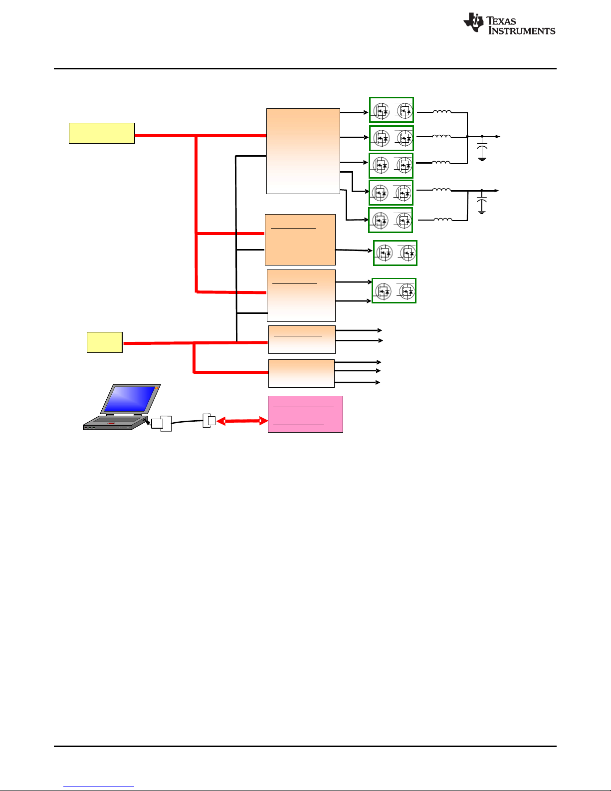
9-20VBAT
CPU Core
(94A)
GPU Core
(46A)
Power Block
IMVP7
TPS59650
48 Pin
6x6 QFN
TPS51219
16 Pin
3x3 QFN
VCCIO: 1.05V/10A
TPS70102PWP
20 Pin
PWP
TPS51916
20 Pin
3x3 QFN
TMS320F2808PZS
TUSB3410RHB
VCCIO: 0A-10A
VDDQ: 1.2V/8A
VTT: 0.6V/2A,
VTTREF: 0.6V/10mA
1.8V/500mA
GPU: 0A-19A
On Board Dynamic
Load for CPU, GPU
and VCCIO
CPU: 0A-32A
SVID
5Vin
3.3V/250mA
Host Computer
B
USB Cable
A
GUI communication
DDR3L/DDR4 Memory Rail
TPS59650EVM-753 Power System Block Diagram
2 TPS59650EVM-753 Power System Block Diagram
www.ti.com
Figure 1. TPS59650EVM-753 Power System Block Diagram
6
Using the TPS59650EVM-753 Intel™ IMVP-7 3-Phase CPU/2-Phase GPU SLUU896–March 2012
SVID Power System
Copyright © 2012, Texas Instruments Incorporated
Submit Documentation Feedback
Page 7
CPU Core
GPU CORE
TPS51219
VCCIO
TPS59650
Chief River CPU
socket
OCL, FSW
selection
TPS51916
DDR3L/DDR4
Memory Rail
Intel SVID GUI
from USB
CPU/GPU
VR_ON
CPU Load
Connector
CSD87350Q5D
GPU Load Connector
www.ti.com
Electrical Performance Specifications
3 Electrical Performance Specifications
PARAMETER TEST CONDITIONS MIN TYP MAX UNITS
INPUT CHARACTERISTICS
12VBAT input voltage range VBAT 9 12 20 V
Maximum input current VBAT = 12V, all full load (3-Phase CPU/2-Phase GPU) 15.5 A
No load input current VBAT=12V, all no load(3-Phase CPU/2 Phase GPU) 0.14 A
5VIN input voltage range 5Vin 4.5 5 5.5 V
Maximum input current VBAT =12 V, all full load 0.3 A
No load input current VBAT=12V, all no load 0.1 A
OUTPUT CHARACTERISTICS
CPU(TPS59650)
Output voltage Vcore SVID: Address:00 CPU, Payload: 1.05V 1.05 V
Output voltage regulation
Output voltage ripple VBAT=12V, 1.05V/90A(3-Phase) at 300kHz 25 mVpp
Output load current CPU 3-Phase operation 0 94 A
Output over current Selectable per phase 37 A
Switching frequency Selectable 250 300 600 kHz
Full load efficiency VBAT=12V, 1.05V/95A at 300kHz 80.05%
GPU(TPS59650)
Output voltage Vcore SVID: Address:01 GPU, Payload: 1.23V 1.23 V
(1)
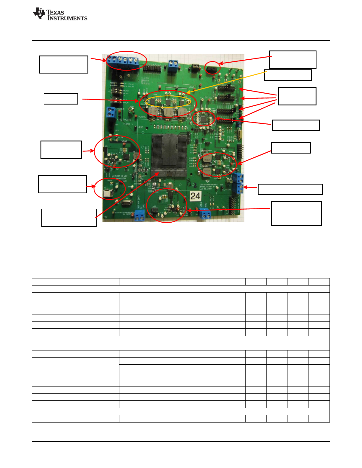
Figure 2. TPS59650EVM-753 EVM Illustration
Table 1. TPS59650EVM-753 Electrical Performance Specifications
Line regulation 0.1%
Load regulation(Droop) Load Line –1.9 mΩ
Jumpers set to default locations, see section 6 of this user’s guide
(1)
SLUU896–March 2012 Using the TPS59650EVM-753 Intel™ IMVP-7 3-Phase CPU/2-Phase GPU
Submit Documentation Feedback
Copyright © 2012, Texas Instruments Incorporated
SVID Power System
7
Page 8

Test Setup
www.ti.com
Table 1. TPS59650EVM-753 Electrical Performance Specifications
PARAMETER TEST CONDITIONS MIN TYP MAX UNITS
Output voltage regulation
Output voltage ripple VBAT=12V, 1.23V/50A 2 Phase at 385kHz 30 mVpp
Output load current 0 50 A
Output over current Selectable per phase 37 A
Switching frequency Selectable 275 385 660 kHz
Full load efficiency VBAT=12V, 1.23V/50A 2 Phase at 385KHz 86.58%
1.05V VCCIO (TPS51219)
Output voltage 1.05 V
Output voltage regulation
Output voltage ripple VBAT=12V, 1.05V/10A 30 mVpp
Output load current 0 10 A
Output over current 16 A
Switching frequency Selectable 500 kHz
Full load efficiency VBAT=12V, 1.05V/10A 89.87%
DDR3L/DDR4 Memory Rail (TPS51916)
Output voltage 1.2 V
Output voltage regulation
Output voltage ripple VBAT=12V, 1.2V/8A 30 mVpp
Output load current 0 8 A
Output over current 10 A
Switching frequency Selectable 500 kHz
Full load efficiency VBAT=12V, 1.2V/8A 89.07%
Operating temperature 25 °C
Line regulation 0.1%
Load regulation(Droop) Load Line –3.9 mΩ
Line regulation 0.1%
Load regulation 0.1%
Line regulation 0.1%
Load regulation 0.1%
(1)
(continued)
4 Test Setup
4.1 Test Equipment
4.1.1 PC Computer (Host Computer)
Microsoft Windows XP or newer with available USB port
4.1.2 USB Cable
The USB Cable: Standard USB_A to USB_B 5 Pin Mini-B cable. See Figure 3 .
Figure 3. USB Cable
8
Using the TPS59650EVM-753 Intel™ IMVP-7 3-Phase CPU/2-Phase GPU SLUU896–March 2012
SVID Power System
Copyright © 2012, Texas Instruments Incorporated
Submit Documentation Feedback
Page 9
www.ti.com
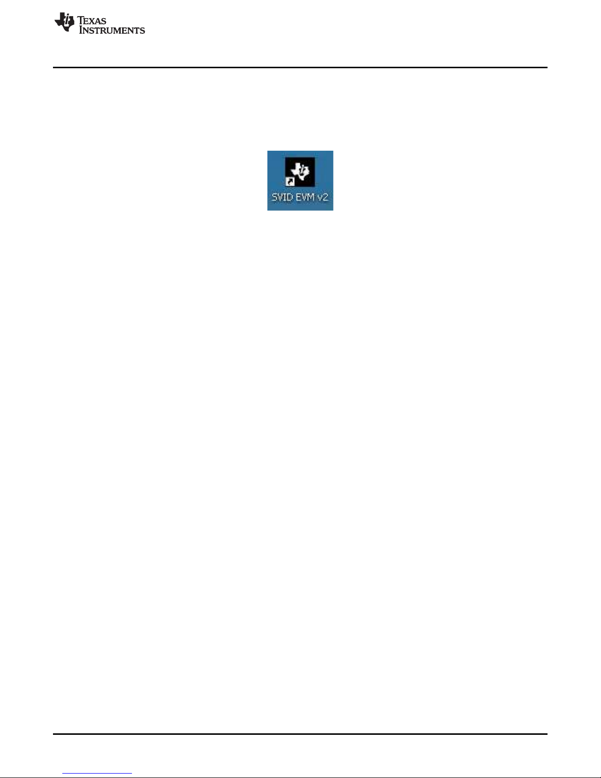
4.1.3 TPS59650 USB driver and SVID GUI Installation
1. Copy the both files: setup.exe and setup.msi to the host computer.
2. Run this setup.exe.
3. Following installation Instructions, this will install the driver and the Texas Instruments SVID GUI.
4. It will add the below icon
4.1.4 DC Source
12VBAT DC Source: The 12VBAT DC source should be a 0-20V variable DC source capable of
supplying 20Adc current. Connect 12VBAT to J21 as shown in Figure 4.
5Vin DC Source: The 5Vin DC source should be a 0-5V variable DC source capable of supplying 1Adc
current. Connect 5Vin to J22 as shown in Figure 4.
4.1.5 Meters
• V1: 5Vin at TP81(5Vin) and TP83(GND)
• V2: 12VBAT at TP82(VBAT) and TP24(GND)
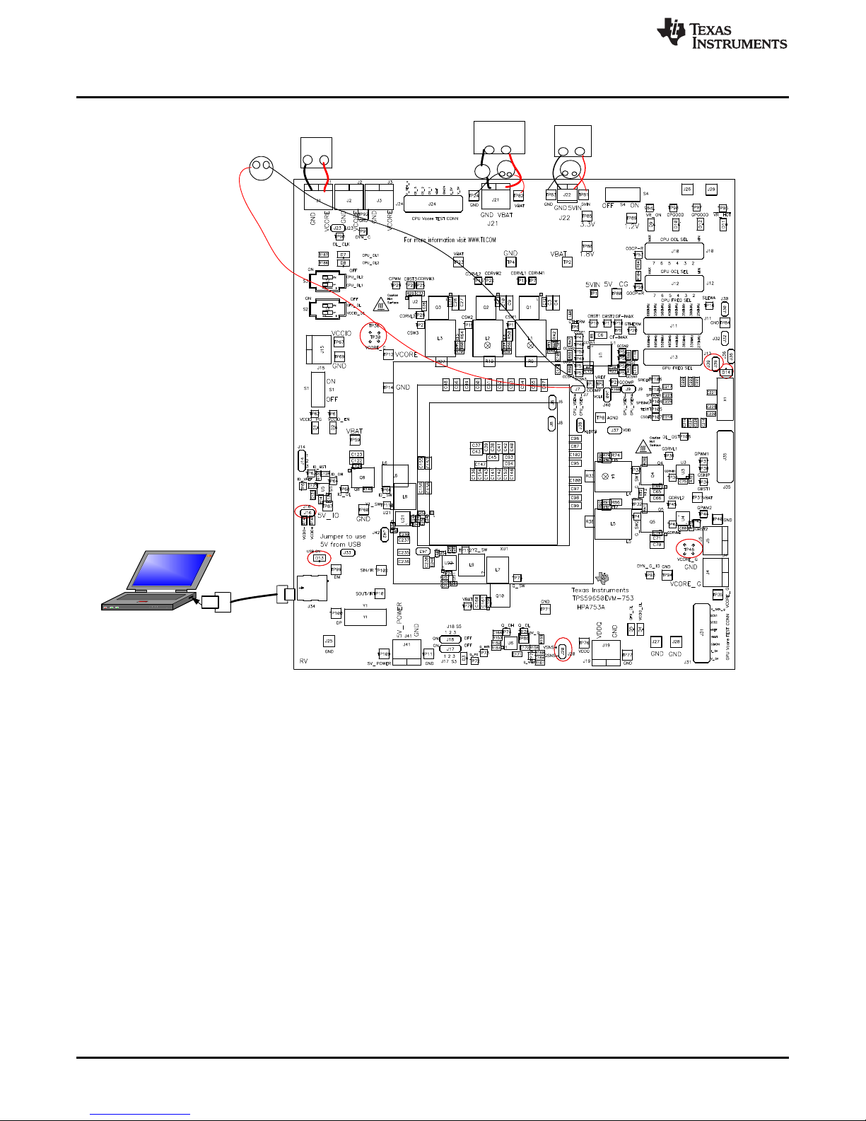
• V3: CPU Vcore sense voltage at J7; GPU Vcore sense voltage at J9; VDDQ sense voltage at J20,
VCCIO sense voltage at J16
• A1: 12VBAT input current
Test Setup
4.1.6 Load
The output load should be an electronic constant current load capable of 0-90Adc.
4.1.7 Oscilloscope
A digital or analog oscilloscope can be used to measure the output ripple. The oscilloscope should be set
for 1MΩ impedance, 20MHz Bandwidth, AC coupling, 2us/division horizontal resolution, 50mV/division
vertical resolution. Test point TP30 and TP46 can be used to measure the output ripple voltage for CPU
and GPU. Do not use a leaded ground connection as this may induce additional noise due to the large
ground loop.
4.2 Recommended Wire Gauge
1. V5in to J22(5V input):
The recommended wire size is 1x AWG #18 per input connection, with the total length of wire less than
4 feet (2 feet input, 2 feet return).
2. 12VBAT to J21(12V input):
The recommended wire size is 1x AWG #16 per input connection, with the total length of wire less than
4 feet (2 feet input, 2 feet return).
3. J1, J2, J3(CPU) to LOAD or J4, J5 (GPU) to LOAD or J19 (VDDQ) to LOAD or J15(VCCIO) to
LOAD:
The minimum recommended wire size is 2x AWG #16, with the total length of wire less than 4 feet (2
feet output, 2 feet return)
4.3 Recommended Test Setup
Figure 4 is the recommended test set up to evaluate the TPS59650EVM-753.Working at an ESD
workstation, make sure that any wrist straps, bootstraps or mats are connected referencing the user to
earth ground before handling the EVM.
SLUU896–March 2012 Using the TPS59650EVM-753 Intel™ IMVP-7 3-Phase CPU/2-Phase GPU
Submit Documentation Feedback
Copyright © 2012, Texas Instruments Incorporated
SVID Power System
9
Page 10
Host Computer
B
USB Cable
A
CPU
V1
- +
5Vin DC
Source
+
-
V2
- +
A1
12VBAT DC
Source
+
-
-
+
++
--
Load
+
-
V3
+
-
VCCIO
+
-
GPU
-
+
VDDQ
_
+
Test Setup
www.ti.com
Figure 4. TPS59650EVM-753 Recommended Test Set Up
4.4 USB Cable Connections
A standard USB_A and 5 pin Mini_B USB cable needed to connect between host computer and J34 USB
port (left bottom side). A GREEN LED(D13) will light up near the USB port on the EVM. This just means
USB cable is connected.
4.5 Input Connections
1. Prior to connecting the 5Vin DC source, it is advisable to limit the source current from 5Vin to 1A
maximum. Make sure 5Vin is initially set to 0V and connected as shown in Figure 4.
2. Prior to connecting the 12VBAT DC source, it is advisable to limit the source current from 12VBAT to
10A maximum. Make sure 12VBAT is initially set to 0V and connected as shown in Figure 4.
3. Connect voltmeters V1 at TP81 (5Vin) and TP83 (GND) to measure 5Vin voltage, V2 at TP82 (VBAT)
and TP24 (GND) to measure 12VBAT voltage as shown in Figure 4.
4. Connect a current meter A1 between 12VBAT DC source and J21 to measure the 12VBAT input
current.
10
Using the TPS59650EVM-753 Intel™ IMVP-7 3-Phase CPU/2-Phase GPU SLUU896–March 2012
SVID Power System
Copyright © 2012, Texas Instruments Incorporated
Submit Documentation Feedback
Page 11
www.ti.com
4.6 Output Connections
1. Connect Load to J1, J2, J3 and set Load to constant resistance mode to sink 0Adc before 5Vin and
12VBAT are applied. This is for CPU operation.
2. Connect a voltmeter V3 at J7 to measure CPU Vcore sense voltage.
5 Configuration
All Jumper selections should be made prior to applying power to the EVM. User can configure this EVM
per following configurations.
5.1 CPU and GPU Configuration
5.1.1 CPU/GPU Current Limit Trip Selection (J10 for CPU and J12 for GPU)
The current limit trip can be set by J10(COCP) and J12(GOCP).
Default setting: Level 5 for both CPU and GPU.
Table 2. Current Limit Trip Selection
Jumper set to Connected Resistor COCP/GOCP Limit (Typ.)
Left (1-2 pin shorted) 150k Max
2nd(3-4 pin shorted) 100k Level 7
3rd(5-6 pin shorted) 75k Level 6
4th(7-8 pin shorted) 56.2k Level 5
5th(9-10 pin shorted) 39.2k Level 4
6th(11-12 pin shorted) 30.1k Level 3
7th(13-14 pin shorted) 24.3k Level 2
Right(15-16 pin shorted) 20.0k Min
Configuration
5.1.2 CPU Frequency Selection (J11)
The operating frequency can be set by J11
Default setting: 300 kHz for CPU
Jumper set to Connected Resistor CPU
Left (1-2 pin shorted) 150k 600 kHz
2nd(3-4 pin shorted) 100k 550 kHz
3rd(5-6 pin shorted) 75k 500 kHz
4th(7-8 pin shorted) 56.2k 450 kHz
5th(9-10 pin shorted) 39.2k 400 kHz
6th(11-12 pin shorted) 30.1k 350 kHz
7th(13-14 pin shorted) 24.3k 300 kHz
Right(15-16 pin shorted) 20.0k 250 kHz
Table 3. CPU Frequency Selection
SLUU896–March 2012 Using the TPS59650EVM-753 Intel™ IMVP-7 3-Phase CPU/2-Phase GPU
Submit Documentation Feedback
Copyright © 2012, Texas Instruments Incorporated
SVID Power System
11
Page 12
Configuration
5.1.3 GPU Frequency Selection (J13)
The operating frequency can be set by J13
Default setting: 385 kHz for GPU.
Table 4. GPU Frequency Selection
Jumper set to Connected Resistor GPU
Left (1-2 pin shorted) 150k 660 kHz
2nd(3-4 pin shorted) 100k 605 kHz
3rd(5-6 pin shorted) 75k 550 kHz
4th(7-8 pin shorted) 56.2k 495 kHz
5th(9-10 pin shorted) 39.2k 440 kHz
6th(11-12 pin shorted) 30.1k 385 kHz
7th(13-14 pin shorted) 24.3k 330 kHz
Right(15-16 pin shorted) 20.0k 275 kHz
5.1.4 F2808 DSP Program Mode Selection (J39)
The F2808 DSP Program Mode(GUI) Selection can be set by J39.
Default setting: No Jumper shorts on J39 for normal operation
Table 5. F2808 DSP Program Mode Selection
Jumper set to Program Mode Selection
No Jumper on J39 Normal Operation
Jumper on J39 Flash the DSP program to the EVM
www.ti.com
5.1.5 5Vin Bias Voltage Option (J33)
The 5Vin Bias Voltage can be used from USB or Externally
Default setting: No Jumper shorts on J33
Table 6. 5Vin Bias Voltage Option (J33)
Jumper set to Selection
No Jumper 5Vin Bias from J22 external
Jumper on J39 5Vin Bias from USB, 5Vin from J22 should not be connected
5.1.6 On Board Dynamic Load Selection (S3 for CPU, S2(upper) for GPU, S2(lower) for VCCIO)
The on board dynamic load can be set by S2 and S3.
Default setting: Push S2 and S3 to “OFF” position to disable the on board dynamic load
Table 7. On Board Dynamic Load Selection
Switch set to Dynamic Load Selection
Push S3 to “ON” position Enable 32A on board dynamic load at CPU
Push S3 to “OFF” position Disable 32A on board dynamic load at CPU
Push S2(upper) to “ON” position Enable 19A on board dynamic load at GPU
Push S2(upper) to “OFF” position Disable 19A on board dynamic load at GPU
Push S2(lower) to “ON” position Enable 10A on board dynamic load at VCCIO
Push S2(lower) to “OFF” position Disable 10A on board dynamic load at VCCIO
12
Using the TPS59650EVM-753 Intel™ IMVP-7 3-Phase CPU/2-Phase GPU SVID SLUU896–March 2012
Power System
Submit Documentation Feedback
Copyright © 2012, Texas Instruments Incorporated
Page 13
www.ti.com
5.1.7 IMVP-7 VR_ON Enable Selection (S4)
The IMVP-7 CPU/GPU can be enabled and disabled by S4
Default setting: Push S4 to “OFF” position to disable both CPU and GPU
Table 8. VR_ON Enable Selection
Switch set to VR_ON Selection
Push S4 to “ON” position Enable IMVP-7 CPU/GPU Vcore
Push S4 to “OFF” position Disable IMVP-7 CPU/GPU Vcore
5.2 1.2VDDQ, 0.6V VTT and 0.6V VTTREF Configuration
5.2.1 VDDQ S3, S5 Enable Selection
The controller can be enabled and disabled by J18 and J17.
Default setting: Jumper shorts on Pin2 and Pin3 of J18,
Def ault setti ng : Jumper shorts on Pin2 and Pin3 of J17
Table 9. VDDQ S3, S5 Enable Selection
State J17 (S3) set to J18(S5) set to VDDQ VTTREF VTT
S0 ON position ON position ON ON ON
S3 OFF position ON position ON ON OFF(High-Z)
S4/S5 OFF position OFF position OFF(Discharge) OFF(Discharge) OFF(Discharge)
Configuration
5.3 1.05V VCCIO Configuration
5.3.1 1.05V Enable Selection (S1)
1.05V Enable can be set by S1
Default setting: Push S1 to ”OFF” position
Table 10. 1.05V Enable Selection
Jumper set to Selection
Push S1 to “ON” position 1.05V Enabled
Push S1 to “OFF” position 1.05V Disabled
5.3.2 VCCIO Output Voltage Selection (J14)
The VCCIO Output Voltage can be selected by J14
Default setting: Jumper shorts Pin1 and Pin2 of J14
Table 11. VCCIO Output Voltage Selection
Jumper set to Selection
Jumper shorts on Pin1 and Pin2 VCCIO: 1.05V
Jumper shorts on Pin2 and Pin3 VCCIO: 1.00V
SLUU896–March 2012 Using the TPS59650EVM-753 Intel™ IMVP-7 3-Phase CPU/2-Phase GPU
Submit Documentation Feedback
Copyright © 2012, Texas Instruments Incorporated
SVID Power System
13
Page 14
Test Procedure
5.3.3 On Board Dyanamic Load Enable Pin (J23)
The on board dynamic load can be enabled or disabled by J23
Default setting: Jumper shorts on J23
Table 12. On Board Dynamic Load Enable/Disable selection
Jumper set to Selection
Jumper shorts Enable on board dynamic load
No Jumper short Disable on board dynamic load
6 Test Procedure
6.1 Line/Load Regulation and Efficiency Measurement Procedure
6.1.1 CPU
1. Set up EVM as described in Section 4.3 through Section 4.6 and Figure 4.
2. Ensure J39 no Jumper shorts on
3. Ensure all other Jumpers configuration setting by Section 5 before 5Vin and 12VBAT are applied.
4. Ensure Load is set to constant resistance mode and to sink 0Adc
5. Ensure S1 and S4 are in “OFF” position
6. Add scope probe on the TP30 for CPU Vcore ripple measurement
7. Ensure USB Cable is connected between host computer and USB port(J34) on the EVM
8. Increase 5Vin from 0V to 5V. Using V1 to measure 5Vin input voltage.
9. Increase 12VBAT from 0V to 12V. Using V2 to measure 12VBAT input voltage.
www.ti.com
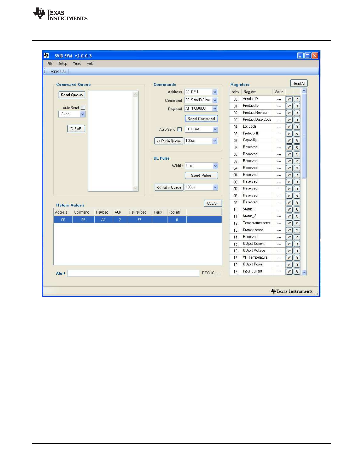
10. Double-Click the icon to launch the GUI program. The GUI window shown in Figure 5.
11. Push S4 to “ON” position to enable the VR_ON of TPS59650. VR_ON LED will light up.
12. Now the user is ready to send SVID commends. The GUI at start-up defaults:
Address: 00 CPU, Commend: SetVIDslow, Payload: 1.05V (The user can select the SVID commend by
using the pull-down menu”)
13. Click “send Commend” and CPU CPGOOD LED will light up, See the GUI window as Figure 5.
14. Measure V3: CPU Vcore at J7 and A1: 12VBAT input current
15. Vary CPU LOAD from 0Adc to 94Adc, CPU Vcore must remain in load line
16. Vary 12VBAT from 9V to 20V CPU Vcore must remain in line regulation
17. Push S4 to “OFF” position to disable CPU Vcore controller.
18. Decrease LOAD to 0A and disconnect the LOAD from terminal J1, J2, J3
19. Disconnect V3 from J7.
20. Disconnect scope probe from TP30
14
Using the TPS59650EVM-753 Intel™ IMVP-7 3-Phase CPU/2-Phase GPU SLUU896–March 2012
SVID Power System
Copyright © 2012, Texas Instruments Incorporated
Submit Documentation Feedback
Page 15
www.ti.com
Test Procedure
Figure 5. TPS59650EVM-753 CPU GUI set up Window
6.1.2 GPU
1. Connect the LOAD to GPU terminal J4, J5 and V3 at J9. Ensure correct polarity.
2. Add scope probe on the TP46 for GPU Vcore_G ripple measurement
3. Push S4 to “ON” position to enable the VR_ON of TPS59650. The VR_ON LED will light up.
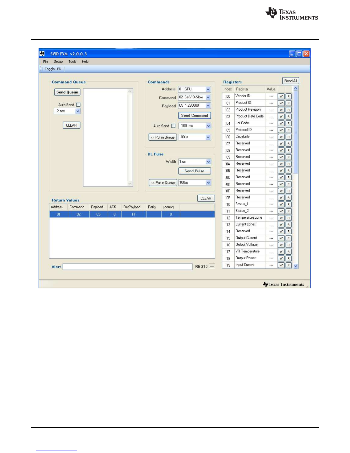
4. Now you are ready to send SVID commends for GPU. Using pull-down menu:
Address: 01 GPU, Commend: SetVIDslow, Payload: 1.23V
5. Click “send Commend” and GPU GPOOD LED will light up, See the GUI window as Figure 6.
SLUU896–March 2012 Using the TPS59650EVM-753 Intel™ IMVP-7 3-Phase CPU/2-Phase GPU
Submit Documentation Feedback
Copyright © 2012, Texas Instruments Incorporated
SVID Power System
15
Page 16
Test Procedure
www.ti.com
Figure 6. TPS59650EVM-753 GPU GUI set up Window
6. Measure V3: GPU Vcore_G at J9 and A1: 12VBAT input current
7. Vary GPU LOAD from 0Adc to 50Adc, GPU Vcore must remain in load line
8. Vary 12VBAT from 9V to 20V GPU Vcore must remain in line regulation
9. Push S4 to “OFF” position to disable GPU Vcore controller.
10. Decrease LOAD to 0A and disconnect the LOAD from terminal J11
11. Disconnect V3 from J9.
12. Disconnect scope probe from TP46
13. Exit SVID GUI window: click File → click Exit
14. Disconnect the USB cable between host Computer and EVM
16
Using the TPS59650EVM-753 Intel™ IMVP-7 3-Phase CPU/2-Phase GPU SLUU896–March 2012
SVID Power System
Copyright © 2012, Texas Instruments Incorporated
Submit Documentation Feedback
Page 17

www.ti.com
6.1.3 VDDQ
1. Connect the LOAD to VDDQ terminal J19 and V3 at J20. Ensure correct polarity.
2. Remove Jumper from J17, J18 from pin2 and pin3 and put this Jumper on pin1 and pin 2 of J18, J17
to enable S5 of VDDQ controller. VDDQ PGOOD LED will light up.
3. Measure V3: VDDQ at J20 and A1: 12Vin input current
4. Vary VDDQ LOAD from 0Adc to 8Adc, VDDQ must remain in the load regulation
5. Vary 12VBAT from 9V to 20V, VDDQ must remain in the line regulation
6. Remove Jumper of J17, J18 and shorts back on pin2 and pin3 of J17, J18 to disable VDDQ controller.
7. Decrease LOAD to 0A and disconnect the LOAD from terminal J19
8. Disconnect V3 from J20.
6.1.4 VCCIO
1. Connect the LOAD to VCCIO terminal J15 and V3 at J16. Ensure correct polarity.
2. Push S1 to “ON” position to enable the VCCIO controller. VCCIO EN and PGOOD LED will light up.
3. Measure V3: VCCIO at J16 and A1: 12Vin input current
4. Vary VDDQ LOAD from 0Adc to 10Adc, VCCIO must remain in the load regulation
5. Vary 12VBAT from 9V to 20V, VCCIO must remain in the line regulation
6. Push S1 to “OFF” position to disable VCCIO controller.
7. Decrease LOAD to 0A and disconnect the LOAD from terminal J15
8. Disconnect V3 from J16.
Test Procedure
6.2 Equipment Shutdown
1. Shut down Load
2. Shut down 12VBAT and 5Vin
3. Shut down oscilloscope
4. Shut down host computer
SLUU896–March 2012 Using the TPS59650EVM-753 Intel™ IMVP-7 3-Phase CPU/2-Phase GPU
Submit Documentation Feedback
Copyright © 2012, Texas Instruments Incorporated
SVID Power System
17
Page 18
0.8
0.85
0.9
0.95
1
1.05
1.1
V - Output Voltage - V
O
0 10 20 30 40 50 60 70 80 90 100
I - Output Current - A
O
V = 12 V
IN
V = 20 V
IN
V = 9 V
IN
SPEC(min)
SPEC(nom)
SPEC(max)
65
70
75
80
85
90
95
Efficiency - %
0 10 20 30 40 50 60 70 80 90 100
I - Output Current - A
O
V = 12 V
IN
V = 20 V
IN
V = 9 V
IN
TPS59650EVM
CPU VR_ON Turn off
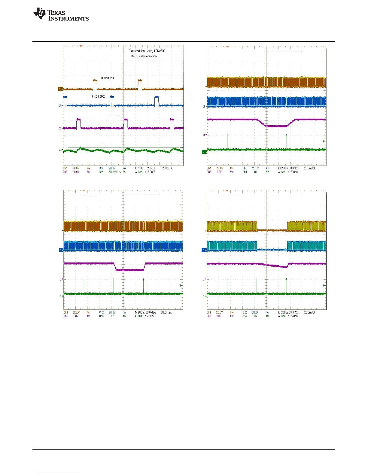
Test condition: 12 Vin, 1.05V/60A
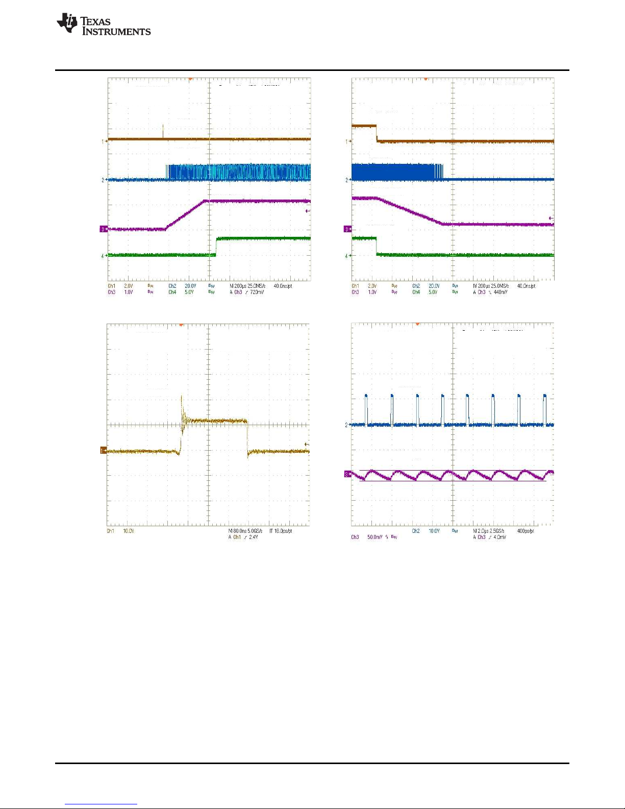
CPU 3 Phase operation
CH4: CPGOOD
CH1: CSW1
CH2: CSW2
CH3: 1.05V core
TPS59650EVM
CPU VDIO Turn on
Test condition: 12 Vin, 1.05V/60A
CPU 3 Phase operation
CH1: CSW1
CH2: CSW2
CH3: 1.05V core
CH4: CPGOOD
Performance Data and Typical Characteristic Curves
7 Performance Data and Typical Characteristic Curves
Figure 7 through Figure 91 present typical performance curves for TPS59650EVM-753. Jumpers set to
default locations, see section 6 of this user’s guide.
7.1 CPU 3-Phase Operation
www.ti.com
Figure 7. CPU3 Efficiency Figure 8. CPU3 Load regulation
18
Using the TPS59650EVM-753 Intel™ IMVP-7 3-Phase CPU/2-Phase GPU SLUU896–March 2012
SVID Power System
Figure 9. CPU3 Enable Turn on Figure 10. CPU3 Enable Turn off
Copyright © 2012, Texas Instruments Incorporated
Submit Documentation Feedback
Page 19
Test condition: 12 Vin, 1.05V/60A
CPU 3 Phase operation
CH1: CSW1
CH2: CSW2
TPS59650EVM
CPU Switching node and Output Ripple
CH3: CSW3
CH4: 1.05V core Ripple
TPS59650EVM
CPU Dynamic VID: Set VID-Slow/Slow
Test condition: 12 Vin, 1.05V/1A
CPU 3 Operation
CH4: VDIO
CH1: CSW1
CH2: CSW2
CH3: 1.05V core
Test condition: 12 Vin, 1.05V/1A
CPU 3 Operation
CH4: VDIO
CH1: CSW1
CH2: CSW2
CH3: 1.05V core
TPS59650EVM
CPU Dynamic VID: Set VID-Fast/fast
TPS59650EVM
CPU Dynamic VID: Set VID-Decay/Fast
Test condition: 12 Vin, 1.05V/1A
CPU 3 Operation
CH4: VDIO
CH1: CSW1
CH2: CSW2
CH3: 1.05V core
www.ti.com
Performance Data and Typical Characteristic Curves
Figure 11. CPU3 Switching Node(Ripple) Figure 12. CPU3 Dynamic VID: SetVID-Slow/Slow
Figure 13. CPU3 Dynamic VID:SetVID-Fast/Fast Figure 14. CPU3 Dynamic VID:SetVID-Decay/Fast
SLUU896–March 2012 Using the TPS59650EVM-753 Intel™ IMVP-7 3-Phase CPU/2-Phase GPU
Submit Documentation Feedback
Copyright © 2012, Texas Instruments Incorporated
SVID Power System
19
Page 20
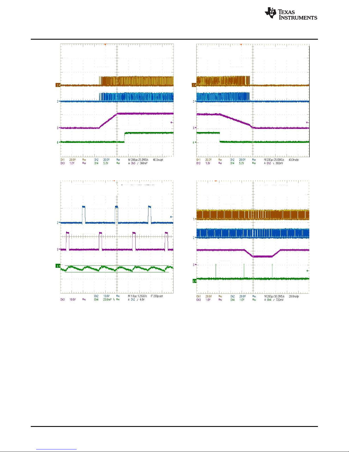
CH1: CSW1
CH2: CSW2
TPS59650EVM
CPU Output Load Releas with
OSR/USR middle level
Test condition: 12 Vin, 1.05V/0A-51A
CPU 3 Phase on board dynamic load
CH3: CSW3
CH4: 1.05V core
TPS59650EVM
CPU Output Load Insertion with
OSR/USR middle level
Test condition: 12 Vin, 1.05V/0A-51A
CPU 3 Phase on board dynamic load
CH1: CSW1
CH2: CSW2
CH4: 1.05V core
CH3: CSW3
Performance Data and Typical Characteristic Curves
Figure 15. CPU3 Output Load Insertion with OSR/USR Figure 16. CPU3 Output Load Release with OSR/USR
middle level middle level
www.ti.com
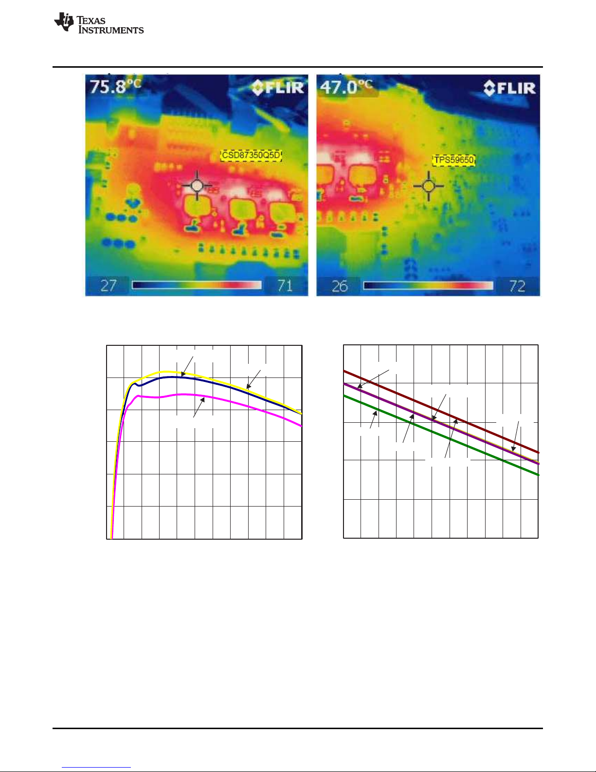
Figure 17. CPU3 Bode Plot at 12Vin, 1.05V/60A
Test condition: CPU3 12Vin, 1.05V/60A no airflow
20
Using the TPS59650EVM-753 Intel™ IMVP-7 3-Phase CPU/2-Phase GPU SLUU896–March 2012
SVID Power System
Copyright © 2012, Texas Instruments Incorporated
Submit Documentation Feedback
Page 21
0.85
0.9
0.95
1
1.05
1.1
V - Output Voltage - V
O
0 5 10 15 20 25 30 35 40 45 50 55
I - Output Current - A
O
SPEC(min)
SPEC(nom)
SPEC(max)
V = 9 V
IN
V = 20 V
IN
V = 12 V
IN
65
70
75
80
85
90
95
Efficiency - %
0 5 10 15 20 25 30 35 40 45 50 55
I - Output Current - A
O
V = 12 V
IN
V = 9 V
IN
V = 20 V
IN
www.ti.com
Figure 18. CPU3 MOSFET Figure 19. CPU3 IC
7.2 CPU 2-Phase Operation
Performance Data and Typical Characteristic Curves
Figure 20. CPU2 Efficiency Figure 21. CPU2 Load regulation
SLUU896–March 2012 Using the TPS59650EVM-753 Intel™ IMVP-7 3-Phase CPU/2-Phase GPU
Submit Documentation Feedback
Copyright © 2012, Texas Instruments Incorporated
SVID Power System
21
Page 22
CH1: CSW1
CH2: CSW2
CH3: 1.05V core
CH4: CPGOOD
TPS59650EVM
CPU VDIO Turn on
Test condition: 12 Vin, 1.05V/40A
CPU 2 Phase Operation
TPS59650EVM
CPU VR_ON Turn off
Test condition: 12 Vin, 1.05V/40A
CPU 2 Phase Operation
CH4: CPGOOD
CH3: 1.05V core
CH2: CSW2
CH1: CSW1
TPS59650EVM
CPU Switching node and Output Ripple
Test condition: 12 Vin, 1.05V/40A
CPU 2 Phase Operation
CH4: 1.05Vcore
CH3: CSW2
CH2: CSW1
TPS59650EVM
CPU Dynamic VID: Set VID-Slow/Slow
Test condition: 12 Vin, 1.05V/1A
CPU 2 Operation
CH1: CSW1
CH2: CSW2
CH3: 1.05Vcore
CH4: VDIO
Performance Data and Typical Characteristic Curves
Figure 22. CPU2 Enable Turn on Figure 23. CPU2 Enable Turn off
www.ti.com
Figure 24. CPU2 Switching Node(Ripple) Figure 25. CPU2 Dynamic VID: SetVID-Slow/Slow
22
Using the TPS59650EVM-753 Intel™ IMVP-7 3-Phase CPU/2-Phase GPU SLUU896–March 2012
SVID Power System
Copyright © 2012, Texas Instruments Incorporated
Submit Documentation Feedback
Page 23

TPS59650EVM
CPU Dynamic VID: Set VID-Decay/Fast
Test condition: 12 Vin, 1.05V/1A
CPU 2 Operation
CH1: CSW1
CH2: CSW2
CH3: 1.05Vcore
CH4: VDIO
TPS59650EVM
CPU Dynamic VID: Set VID-Slow/Slow
Test condition: 12 Vin, 1.05V/1A
CPU 2 Operation
CH1: CSW1
CH2: CSW2
CH3: 1.05Vcore
CH4: VDIO
CH3: CSW2
CH4: 1.05Vcore
TPS59650EVM
CPU Output Load Release with
OSR/USR middle level
Test condition: 12 Vin, 1.05V/0A-51A
CPU 3 Phase on board dynamic load
CH2: CSW1
CH1: DYN_C
CH3: CSW2
CH4: 1.05Vcore
TPS59650EVM
CPU Output Load Insertion with
OSR/USR middle level
Test condition: 12 Vin, 1.05V/0A-51A
CPU 3 Phase on board dynamic load
CH1: DYN_C
CH2: CSW1
www.ti.com
Performance Data and Typical Characteristic Curves
Figure 26. CPU2 Dynamic VID:SetVID-Fast/Fast Figure 27. CPU2 Dynamic VID:SetVID-Decay/Fast
Figure 28. CPU2 Output Load Insertion with OSR/USR Figure 29. CPU2 Output Load Release with OSR/USR
middle level middle level
SLUU896–March 2012 Using the TPS59650EVM-753 Intel™ IMVP-7 3-Phase CPU/2-Phase GPU
Submit Documentation Feedback
Copyright © 2012, Texas Instruments Incorporated
SVID Power System
23
Page 24

Performance Data and Typical Characteristic Curves
www.ti.com
Figure 30. CPU2 Bode Plot at 12Vin, 1.05V/55A
Test condition: CPU2 12Vin, 1.05V/55A no airflow
Figure 31. CPU2 MOSFET Figure 32. CPU2 IC
24
Using the TPS59650EVM-753 Intel™ IMVP-7 3-Phase CPU/2-Phase GPU SLUU896–March 2012
SVID Power System
Copyright © 2012, Texas Instruments Incorporated
Submit Documentation Feedback
Page 25

0 5 10 15 20 25 30 35
I - Output Current - A
O
70
75
80
85
90
95
Efficiency - %
V = 12 V
IN
V = 9 V
IN
V = 20 V
IN
0.9
0.95
1
1.05
1.1
V - Output Voltage - V
O
0 5 10 15 20 25 30 35
I - Output Current - A
O
V = 9 V
IN
SPEC(max)
SPEC(nom)
SPEC(min)
V = 20 V
IN
V = 12 V
IN
CH4: CPGOOD
TPS59650EVM
CPU VDIO Turn on
Test condition: 12 Vin, 1.05V/20A
CPU 3 Phase on board dynamic load
CH2: CSW1
CH1: VDIO
CH3: 1.05Vcore
CH3: 1.05Vcore
CH1: VR_ON
TPS59650EVM
CPU VR_ON Turn off
Test condition: 12 Vin, 1.05V/20A
CPU 1 Phase operation
CH2: CSW1
CH4: CPGOOD
www.ti.com
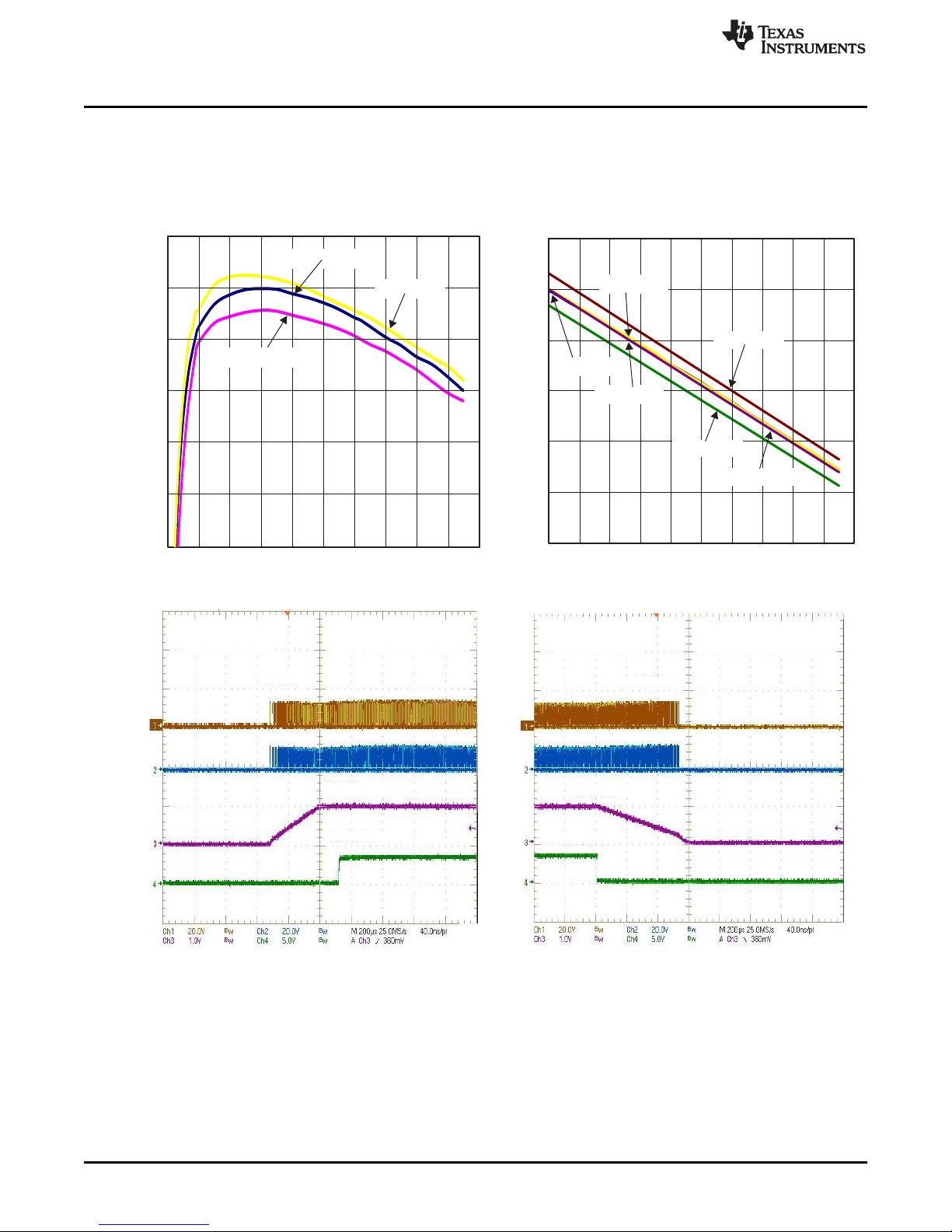
7.3 CPU1-Phase Operation
Figure 33. CPU1 Efficiency Figure 34. CPU1 Load regulation
Performance Data and Typical Characteristic Curves
Figure 35. CPU1 Enable Turn on Figure 36. CPU1 Enable Turn off
SLUU896–March 2012 Using the TPS59650EVM-753 Intel™ IMVP-7 3-Phase CPU/2-Phase GPU
Submit Documentation Feedback
Copyright © 2012, Texas Instruments Incorporated
SVID Power System
25
Page 26

TPS59650EVM
CPU Switching Node
Test condition: 12 Vin, 1.05V/20A
CPU 1 Phase operation
CH1: CSW1
CH2: 1.05Vcore Ripple
CH1: CSW1
TPS59650EVM
CPU Switching Node and Output Ripple
Test condition: 12 Vin, 1.05V/20A
CPU 1 Phase operation
CH3: 1.05Vcore
CH4: VDIO
TPS59650EVM
CPU Dynamic VID: Set VID-Fast/Fast
Test condition: 12 Vin, 1.05V/1A
CPU 1 Operation
CH1: CSW1
CH3: 1.05Vcore
CH4: VDIO
TPS59650EVM
CPU Dynamic VID: Set VID-Slow/Slow
Test condition: 12 Vin, 1.05V/21A
CPU 1 Operation
CH1: CSW1
Performance Data and Typical Characteristic Curves
Figure 37. CPU1 Switching Node Figure 38. CPU1 Switching node and Ripple
www.ti.com
Figure 39. CPU1 Dynamic VID:SetVID-Slow/Slow Figure 40. CPU1 Dynamic VID:SetVID-Fast/Fast
26
Using the TPS59650EVM-753 Intel™ IMVP-7 3-Phase CPU/2-Phase GPU SLUU896–March 2012
SVID Power System
Copyright © 2012, Texas Instruments Incorporated
Submit Documentation Feedback
Page 27

CH3: 1.05Vcore
CH4: VDIO
TPS59650EVM
CPU Dynamic VID: Set VID-Decay/Fast
Test condition: 12 Vin, 1.05V/1A
CPU 1 Operation
CH1: CSW1
CH3: 1.05Vcore
TPS59650EVM
CPU Output Load Insertion with
OSR/USR middle level
Test condition: 12 Vin, 1.05V/0A-27A
CPU 1 Phase on board dynamic load
CH2: CSW1
CH1: DYN_C
CH3: 1.05Vcore
TPS59650EVM
CPU Output Load Releas with
OSR/USR middle level
Test condition: 12 Vin, 1.05V/0A-27A
CPU 1 Phase on board dynamic load
CH2: CSW1
CH1: DYN_C
www.ti.com
Performance Data and Typical Characteristic Curves
Figure 41. CPU1 Dynamic VID:SetVID-Decay/Fast Figure 42. CPU1 Output Load Insertion with OSR/USR
middle level
Figure 43. CPU1 Output Load Release with OSR/USR middle level
SLUU896–March 2012 Using the TPS59650EVM-753 Intel™ IMVP-7 3-Phase CPU/2-Phase GPU
Submit Documentation Feedback
Copyright © 2012, Texas Instruments Incorporated
SVID Power System
27
Page 28

Performance Data and Typical Characteristic Curves
www.ti.com
Figure 44. CPU1 Bode Plot at 12Vin, 1.05V/33A
Test condition: CPU1 12Vin, 1.05V/33A no airflow
Figure 45. CPU1 MOSFET Figure 46. CPU1 IC
28
Using the TPS59650EVM-753 Intel™ IMVP-7 3-Phase CPU/2-Phase GPU SLUU896–March 2012
SVID Power System
Copyright © 2012, Texas Instruments Incorporated
Submit Documentation Feedback
Page 29

70
75
80
85
90
95
Efficiency - %
V = 20 V
IN
V = 12 V
IN
V = 9 V
IN
0 5 10 15 20 25 30 35 40 45 50
I - Output Current - A
O
V - Output Voltage - V
O
0 5 10 15 20 25 30 35 40 45 50
I - Output Current - A
O
1
1.05
1.1
1.15
1.2
1.25
1.3
V = 12 V
IN
V = 9 V
IN
V = 20 V
IN
SPEC(min)
SPEC(max)
SPEC(nom)
CH3: 1.23Vcore
TPS59650EVM
GPU VDIO Turn on
Test condition: 12 Vin, 1.23V/40A
GPU 2 Phase operation
CH2: GSW2
CH4: GPGOOD
CH1: GSW1
CH3: 1.23Vcore
CH1: GSW1
Test condition: 12 Vin, 1.23V/40A
GPU 2 Phase operation
CH2: GSW2
CH4: GPGOOD
TPS59650EVM
GPU VR_ON Turn off
www.ti.com
7.4 GPU 2 Phase Operation
Figure 47. GPU2 Efficiency Figure 48. GPU2 Load regulation
Performance Data and Typical Characteristic Curves
Figure 49. GPU2 Enable Turn on Figure 50. GPU2 Enable Turn off
SLUU896–March 2012 Using the TPS59650EVM-753 Intel™ IMVP-7 3-Phase CPU/2-Phase GPU
Submit Documentation Feedback
Copyright © 2012, Texas Instruments Incorporated
SVID Power System
29
Page 30

CH3: GSW2
CH4: 1.23Vcore Ripple
TPS59650EVM
GPU Switching Node and Output Ripple
Test condition: 12 Vin, 1.23V/20A
GPU 2 Phase operation
CH2: GSW1
Test condition: 12 Vin, 1.23V/1A
GPU 2 Operation
CH2: GSW2
TPS59650EVM
GPU Dynamic VID: Set VID-Slow/Slow
CH1: GSW1
CH3: 1.23Vcore_G
CH4: VDIO
TPS59650EVM
GPU Dynamic VID: Set VID-Decay/Fast
CH1: GSW1
CH3: 1.23Vcore_G
CH4: VDIO
Test condition: 12 Vin, 1.23V/1A
GPU 2 Operation
CH2: GSW2
TPS59650EVM
GPU Dynamic VID: Set VID-Fast/Fast
CH1: GSW1
CH3: 1.23Vcore_G
CH4: VDIO
Test condition: 12 Vin, 1.23V/1A
GPU 2 Operation
CH2: GSW2
Performance Data and Typical Characteristic Curves
Figure 51. GPU2 Switching Node and Ripple Figure 52. GPU2 Dynamic VID:SetVID-Slow/Slow
www.ti.com
Figure 53. GPU2 Dynamic VID:SetVID-Fast/Fast Figure 54. GPU2 Dynamic VID:SetVID-Decay/Fast
30
Using the TPS59650EVM-753 Intel™ IMVP-7 3-Phase CPU/2-Phase GPU SLUU896–March 2012
SVID Power System
Copyright © 2012, Texas Instruments Incorporated
Submit Documentation Feedback
Page 31

TPS59650EVM
GPU Output Load Insertion with OSR/USR
least reduction
CH4: 1.23Vcore
CH3: GSW2
Test condition: 12 Vin, 1.23V/0A-18A
GPU 2 Phase on board dynamic load
CH2: GSW1
CH1: DYN_G
CH1: DYN_G
TPS59650EVM
GPU Output Load Release with OSR/USR
least reduction
Test condition: 12 Vin, 1.23V/0A-18A
GPU 2 Phase on board dynamic load
CH2: GSW1
CH4: 1.23Vcore
CH3: GSW2
www.ti.com
Figure 55. GPU2 Output Load Insertion with OSR/USR Figure 56. GPU2 Output Load Release with OSR/USR
Performance Data and Typical Characteristic Curves
OFF OFF
Figure 57. GPU2 Bode Plot at 12Vin, 1.23V/50A
Test condition: GPU2 12Vin, 1.23V/50A no airflow
SLUU896–March 2012 Using the TPS59650EVM-753 Intel™ IMVP-7 3-Phase CPU/2-Phase GPU
Submit Documentation Feedback
Copyright © 2012, Texas Instruments Incorporated
SVID Power System
31
Page 32

V = 9 V
IN
V = 20 V
IN
V = 12 V
IN
70
75
80
85
90
95
Efficiency - %
0 5 10 15 20 25 30 35
I - Output Current - A
O
1.05
1.1
1.15
1.2
1.25
1.3
V = 9 V
IN
SPEC(max)
SPEC(nom)
SPEC(min)
V = 20 V
IN
V = 12 V
IN
0 5 10 15 20 25 30 35
I - Output Current - A
O
V - Output Voltage - V
O
Performance Data and Typical Characteristic Curves
Figure 58. GPU2 MOSFET Figure 59. GPU2 IC
7.5 GPU 1 Phase Operation
www.ti.com
Figure 60. GPU1 Efficiency Figure 61. GPU1 Load regulation
32
Using the TPS59650EVM-753 Intel™ IMVP-7 3-Phase CPU/2-Phase GPU SLUU896–March 2012
SVID Power System
Copyright © 2012, Texas Instruments Incorporated
Submit Documentation Feedback
Page 33
CH3: 1.23Vcore
CH1: VDIO
TPS59650EVM
GPU VDIO Turn on
Test condition: 12 Vin, 1.05V/20A
GPU 1 Phase operation
CH2: GSW1
CH4: GPGOOD
CH3: 1.23Vcore
CH1: VR_ON
TPS59650EVM
GPU VR_ON Turn on
Test condition: 12 Vin, 1.23V/20A
GPU 1 Phase operation
CH2: GSW1
CH4: GPGOOD
TPS59650EVM
GPU Switching Node
Test condition: 12 Vin, 1.23V/0A-18A
GPU 1 Phase operation
CH1: GSW1
TPS59650EVM
GPU Switching Node and Output Ripple
Test condition: 12 Vin, 1.23V/20A
GPU 1 Phase operation
CH2: GSW1
CH3: 1.23Vcore Ripple
www.ti.com
Performance Data and Typical Characteristic Curves
Figure 62. GPU1 Enable Turn on Figure 63. GPU1 Enable Turn off
Figure 64. GPU1 Switching Node Figure 65. GPU1 Switching Node and Ripple
SLUU896–March 2012 Using the TPS59650EVM-753 Intel™ IMVP-7 3-Phase CPU/2-Phase GPU
Submit Documentation Feedback
Copyright © 2012, Texas Instruments Incorporated
SVID Power System
33
Page 34

TPS59650EVM
CPU Dynamic VID: Set VID-Fast/Fast
Test condition: 12 Vin, 1.23V/1A
GPU 1 Operation
CH1: CSW1
CH3: 1.23Vcore_G
CH4: VDIO
TPS59650EVM
GPU Dynamic VID: Set VID-Slow/Slow
CH1: GSW1
CH3: 1.23Vcore_G
CH4: VDIO
Test condition: 12 Vin, 1.23V/1A
GPU 1 Operation
TPS59650EVM
GPU Dynamic VID: Set VID-Decay/Fast
Test condition: 12 Vin, 1.23V/1A
GPU 1 Operation
CH1: GSW1
CH3: 1.23Vcore_G
CH4: VDIO
CH1: DYN_G
TPS59650EVM
GPU Output Load Insertion with OSR/USR
least reduction
Test condition: 12 Vin, 1.23V/0A-18A
GPU 1 Phase on board dynamic load
CH2: GSW1
CH3: 1.23Vcore
Performance Data and Typical Characteristic Curves
Figure 66. GPU1 Dynamic VID:SetVID-Slow/Slow Figure 67. GPU1 Dynamic VID:SetVID-Fast/Fast
www.ti.com
Figure 68. GPU1 Dynamic VID:SetVID-Decay/Fast Figure 69. GPU1 Output Load Insertion with OSR/USR
34
Using the TPS59650EVM-753 Intel™ IMVP-7 3-Phase CPU/2-Phase GPU SLUU896–March 2012
SVID Power System
Copyright © 2012, Texas Instruments Incorporated
OFF
Submit Documentation Feedback
Page 35

CH1: DYN_G
TPS59650EVM
GPU Output Load Release with OSR/USR
least reduction
Test condition: 12 Vin, 1.23V/0A-18A
GPU 1 Phase on board dynamic load
CH2: GSW1
CH3: 1.23Vcore
www.ti.com
Performance Data and Typical Characteristic Curves
Figure 70. GPU1 Output Load Release with OSR/USR OFF
Figure 71. GPU1 Bode Plot at 12Vin, 1.23V/33A
Test condition: GPU1 12Vin, 1.23V/33A no airflow
SLUU896–March 2012 Using the TPS59650EVM-753 Intel™ IMVP-7 3-Phase CPU/2-Phase GPU
Submit Documentation Feedback
Copyright © 2012, Texas Instruments Incorporated
SVID Power System
35
Page 36

I - Output Current - A
O
0.001 0.01 0.1 1 10 100
0
10
20
30
40
50
60
70
80
90
100
Efficiency - %
V = 9 V
IN
V = 20 V
IN
V = 12 V
IN
0 2 4 6 8 10
I - Output Current - A
O
1.02
1.04
1.06
1.08
V - Output Voltage - V
O
V = 9 V
IN
V = 20 V
IN
V = 12 V
IN
Performance Data and Typical Characteristic Curves
Figure 72. GPU1 MOSFET Figure 73. GPU1 IC
7.6 1.05V VCCIO
www.ti.com
Figure 74. 1.05V Efficiency Figure 75. 1.05V Load regulation
36
Using the TPS59650EVM-753 Intel™ IMVP-7 3-Phase CPU/2-Phase GPU SLUU896–March 2012
SVID Power System
Copyright © 2012, Texas Instruments Incorporated
Submit Documentation Feedback
Page 37

CH3: VCCIO_PG
CH1: VCCIO_EN
TPS59650EVM
VCCIO Enable Turn on
Test condition: 12 Vin, 1.05VCCIO/10A
CH2: 1.05VCCIO
CH3: VCCIO_PG
CH1: VCCIO_EN
TPS59650EVM
VCCIO Enable Turn off
Test condition: 12 Vin, 1.05VCCIO/10A
CH2: 1.05VCCIO
CH1: SW
TPS59650EVM
VCCIO Switching Node
Test condition: 12 Vin, 1.05VCCIO/10A
CH1: VCCIO Output Ripple
TPS59650EVM
VCCIO Output Ripple
Test condition: 12 Vin, 1.05VCCIO/10A
www.ti.com
Performance Data and Typical Characteristic Curves
Figure 76. 1.05V Enable Turn on Figure 77. 1.05V Enable Turn off
Figure 78. 1.05V Switching Node Figure 79. 1.05V Ripple
SLUU896–March 2012 Using the TPS59650EVM-753 Intel™ IMVP-7 3-Phase CPU/2-Phase GPU
Submit Documentation Feedback
Copyright © 2012, Texas Instruments Incorporated
SVID Power System
37
Page 38

CH1: VCCIO Output
TPS59650EVM
VCCIO Output Transient from
DCM to CCM
Test condition: 12 Vin, 1.05VCCIO/0A-10A
CH2: VCCIO Output current
CH1: VCCIO Output
TPS59650EVM
VCCIO Output Transient from
CCM to DCM
Test condition: 12 Vin, 1.05VCCIO/0A-10A
CH2: VCCIO Output current
Performance Data and Typical Characteristic Curves
Figure 80. 1.05V Transient DCM TO CCM Figure 81. 1.05V Transient CCM to DCM
Test condition: 12Vin, 1.05V/10A no airflow
www.ti.com
38
Using the TPS59650EVM-753 Intel™ IMVP-7 3-Phase CPU/2-Phase GPU SLUU896–March 2012
SVID Power System
Figure 82. TPS51219 Thermal
Copyright © 2012, Texas Instruments Incorporated
Submit Documentation Feedback
Page 39

0
10
20
30
40
50
60
70
80
90
100
Efficiency - %
I - Output Current - A
O
0.001 0.01 0.1 1 10
V = 9 V
IN
V = 20 V
IN
V = 12 V
IN
0 2 4 6 8
I - Output Current - A
O
1.14
1.16
1.18
1.20
1.22
1.24
1.26
V - Output Voltage - V
O
V = 9 V
IN
V = 20 V
IN
V = 12 V
IN
CH3: VTTREF
CH1: VDDQ S5
TPS59650EVM
VDDQ S5 Turn on
Test condition: 12 Vin, 1.2VDDQ/8A
CH2: VDDQ
CH4: VDDQ_PG
CH4: VDDQ_PG
CH3: VTTREF
CH2: VDDQ
CH1: VDDQ S5
Test condition: 12 Vin, 1.2VDDQ/8A
TPS59650EVM
VDDQ S5 Turn off
www.ti.com
7.7 1.2V VDDQ
Performance Data and Typical Characteristic Curves
Figure 83. 1.2V Efficiency Figure 84. 1.2V Load regulation
SLUU896–March 2012 Using the TPS59650EVM-753 Intel™ IMVP-7 3-Phase CPU/2-Phase GPU
Submit Documentation Feedback
Figure 85. 1.2V Enable Turn on Figure 86. 1.2V Enable Turn off
Copyright © 2012, Texas Instruments Incorporated
SVID Power System
39
Page 40

CH1: VDDQ Output Ripple
Test condition: 12 Vin, 1.2VDDQ/8A
TPS59650EVM
VDDQ Output Ripple
CH1: VDDQ SW
Test condition: 12 Vin, 1.2VDDQ/8A
TPS59650EVM
VDDQ Output Switching Node
CH4: VDDQ Output current
CH1: VDDQ Output
TPS59650EVM
VDDQ Output transient
from DCM to CCM
Test condition: 12 Vin, 1.2VDDQ/0A-8A
CH4: VDDQ Output current
CH1: VDDQ Output
Test condition: 12 Vin, 1.2VDDQ/0A-8A
TPS59650EVM
VDDQ Output transient
from CCM to DCM
Performance Data and Typical Characteristic Curves
Figure 87. 1.2V Switching Node Figure 88. 1.2V Ripple
www.ti.com
Figure 89. 1.2V Transient DCM TO CCM Figure 90. 1.2V Transient CCM to DCM
Test condition: 12Vin, 1.2V/7.5A no airflow
40
Using the TPS59650EVM-753 Intel™ IMVP-7 3-Phase CPU/2-Phase GPU SLUU896–March 2012
SVID Power System
Copyright © 2012, Texas Instruments Incorporated
Submit Documentation Feedback
Page 41

www.ti.com
Performance Data and Typical Characteristic Curves
Figure 91. TPS51916 Thermal
SLUU896–March 2012 Using the TPS59650EVM-753 Intel™ IMVP-7 3-Phase CPU/2-Phase GPU
Submit Documentation Feedback
Copyright © 2012, Texas Instruments Incorporated
SVID Power System
41
Page 42
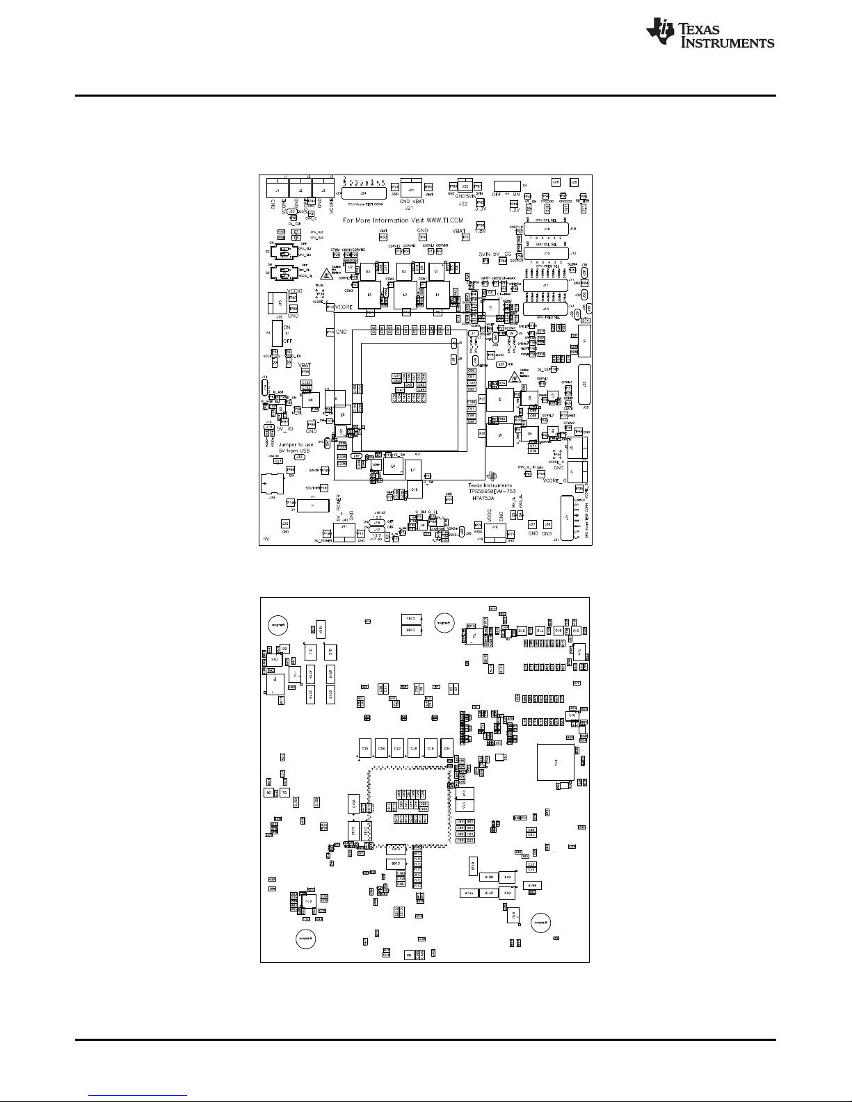
EVM Assembly Drawings and PCB Layout
8 EVM Assembly Drawings and PCB Layout
The following figures (Figure 92 through Figure 101) show the design of the TPS59650EVM-753 printed
circuit board. The EVM has been designed using 8 Layers circuit board with 1oz copper on outside layers.
www.ti.com
Figure 92. TPS59650EVM-753 Top Layer Assembly Drawing (Top view)
Figure 93. TPS59650EVM-753 Bottom Assembly Drawing (Bottom view)
42
Using the TPS59650EVM-753 Intel™ IMVP-7 3-Phase CPU/2-Phase GPU SLUU896–March 2012
SVID Power System
Copyright © 2012, Texas Instruments Incorporated
Submit Documentation Feedback
Page 43

www.ti.com
EVM Assembly Drawings and PCB Layout
Figure 94. TPS59650EVM-753 Top Copper
Figure 95. TPS59650EVM-753 Bottom Copper
SLUU896–March 2012 Using the TPS59650EVM-753 Intel™ IMVP-7 3-Phase CPU/2-Phase GPU
Submit Documentation Feedback
Copyright © 2012, Texas Instruments Incorporated
SVID Power System
43
Page 44

EVM Assembly Drawings and PCB Layout
Figure 96. TPS59650EVM-753 Internal Layer 2
www.ti.com
Figure 97. TPS59650EVM-753 Internal Layer 3
44
Using the TPS59650EVM-753 Intel™ IMVP-7 3-Phase CPU/2-Phase GPU SLUU896–March 2012
SVID Power System
Copyright © 2012, Texas Instruments Incorporated
Submit Documentation Feedback
Page 45

www.ti.com
EVM Assembly Drawings and PCB Layout
Figure 98. TPS59650EVM-753 Internal Layer 4
Figure 99. TPS59650EVM-753 Internal Layer 5
SLUU896–March 2012 Using the TPS59650EVM-753 Intel™ IMVP-7 3-Phase CPU/2-Phase GPU
Submit Documentation Feedback
Copyright © 2012, Texas Instruments Incorporated
SVID Power System
45
Page 46

EVM Assembly Drawings and PCB Layout
Figure 100. TPS59650EVM-753 Internal Layer 6
www.ti.com
Figure 101. TPS59650EVM-753 Internal Layer 7
46
Using the TPS59650EVM-753 Intel™ IMVP-7 3-Phase CPU/2-Phase GPU SLUU896–March 2012
SVID Power System
Copyright © 2012, Texas Instruments Incorporated
Submit Documentation Feedback
Page 47

www.ti.com
Bill of Materials
9 Bill of Materials
The EVM major components list according to the schematic shown in the following pages.
Table 13. EVM Major Components List
QTY REF DES Description MFR Part Number
C1, C12, C31, C69, C74,
11 C124, C159, C121, C130, Capacitor, Ceramic, 1nF, 50V, X7R, 10%, 0603 STD STD
C184, C204
C104, C108, C112, C115,
5 Capacitor, Ceramic, 33nF, 25V, X7R, 10%, 0603 STD STD
C118
C128, C164, C198, C199,
C201, C127, C172, C188,
C192, C203, C207, C190,
C209, C210, C216, C217,
29 Capacitor, Ceramic, 0.1uF, 25V, X7R, 10%, 0603 STD STD
C218, C219, C220, C221,
C222, C223, C224, C225,
C226, C227, C228, C229,
C230
3 C129, C133, C168 Capacitor, Polymer, 330uF, 2V, 6mohm, 20%, 7343 Sanyo 2TPF330M6
2 C13, C26 Capacitor, Ceramic, 100pF, 50V, C0G, 10%, 0603 STD STD
3 C131, C239, C246 Capacitor, Ceramic, 10nF, 50V, X7R, 10%, 0603 STD STD
C15, C16, C19, C20, C76,
6 Capacitor, Polymer, 470uF, 2V, 4mohm, 20%, D2T Sanyo 2TPLF470M4E
C77
1 C166 Capacitor, Ceramic, 2.2uF, 6.3V, X5R, 10%, 0805 STD STD
1 C17 Capacitor, Ceramic, 0.33uF, 6.3V, X7R, 10%, 0603 STD STD
1 C171 Capacitor, Ceramic, 0.22uF, 50V, X7R, 10%, 0603 STD STD
C18, C23, C33, C75, C80,
C196, C202, C208, C195,
15 Capacitor, Ceramic, 1uF, 25V, X7R, 10%, 0603 STD STD
C200, C242, C250, C22,
C233, C234
C193, C36, C79, C82, C7,
7 Capacitor, Ceramic, 2.2uF, 6.3V, X5R, 10%, 0603 STD STD
C135, C170
3 C194, C197, C215 Capacitor, Ceramic, 0.01uF, 50V, X7R, 10%, 0603 STD STD
C2, C3, C4, C5, C8, C9, C10,
C11, C27, C28, C29, C30,
C65, C66, C67, C68, C70,
28 Capacitor, Ceramic, 10uF, 25V, X7R, 20%, 1206 STD STD
C71, C72, C73, C122, C123,
C125, C126, C160, C161,
C162, C163
2 C205, C206 Capacitor, Ceramic, 10pF, 50V, C0G, 10%, 0603 STD STD
2 C213, C214 Capacitor, Ceramic, 22pF, 50V, C0G, 10%, 0603 STD STD
2 C240, C248 Capacitor, Ceramic, 0.22uF, 25V, X7R, 10%, 0402 STD STD
2 C241, C249 Capacitor, Ceramic, 220pF, 25V, X7R, 10%, 0402 STD STD
2 C243, C251 Capacitor, Ceramic, 680pF, 25V, X7R, 10%, 0402 STD STD
2 C244, C252 Capacitor, Ceramic, 100pF, 25V, C0G, 10%, 0402 STD STD
2 C245, C253 Capacitor, Ceramic, 1.8nF, 25V, X7R, 10%, 0402 STD STD
2 C247, C254 Capacitor, Ceramic, 2200pF, 25V, X7R, 10%, 0402 STD STD
44 C37, C38, C39, C40, C41, Capacitor, Ceramic, 22uF, 6.3V, X5R, 10%, 0805 STD STD
C42, C43, C45, C49, C50,
C51, C52, C53, C54, C55,
C56, C87, C88, C89, C90,
C91, C92, C93, C94, C95,
C100, C101, C102, C136,
C140, C141, C143, C145,
C146, C147, C148, C150,
C151, C152, C154, C235,
C236, C237, C238
C44, C46, C57, C58, C59,
C60, C61, C62, C63, C64,
20 C173, C174, C175, C176, Capacitor, Ceramic, 10uF, 6.3V, X5R, 10%, 0805 STD STD
C180, C182, C165, C185,
C189, C191
1 C6 Capacitor, Ceramic, 4.7uF, 6.3V, X5R, 10%, 0805 STD STD
D1, D2, D3, D9, D10, D12,
8 Diode, LED, Green Clear, 20mcd, 0.079x0.049 Lite On LTST-C170GKT
D13, D14
SLUU896–March 2012 Using the TPS59650EVM-753 Intel™ IMVP-7 3-Phase CPU/2-Phase GPU
Submit Documentation Feedback
Copyright © 2012, Texas Instruments Incorporated
SVID Power System
47
Page 48

Bill of Materials
Table 13. EVM Major Components List (continued)
QTY REF DES Description MFR Part Number
5 D4, D5, D7, D8, D11 Diode, LED, Red Clear, 20mcd, 0.079x0.049 Lite On LTST-C170CKT
1 D6 Diode, Schottky, 200mA, 30V, SOT-23, Vishay-Liteon BAT54-V-GS08
1 FB1 Bead, SMD,Ferrite, 100MHz Max, 200mA, +/-25%, 0603 WE 74279266A
5 L1, L2, L3, L4, L5 Inductor, SMT, 0.36uH, 35A , 0.82mohm, 10x11.5mm Toko FCUL1040-H-R36M
1 L6 Inductor, SMT, 0.42uH, 17A , 1.5mohm, 8.7x7.0mm Panasonic ETQP4LR42AFM
1 L7 Inductor, SMT, 1.0uH, 8.1A , 6.9mohm, 7.3x6.6mm Panasonic ETQP3W1R0WFN
7 Q1, Q2, Q3, Q4, Q5, Q8, Q10 MOSFET, Synchronous Buck NexFET Power Block SON 5X6mm TI CSD87350Q5D
4 Q11, Q12, Q13, Q14 MOSFET, Nchan, 25V, 31A, 2.5mohm, QFN5X6mm TI CSD16407Q5
1 Q15 MOSFET, Pchan, -60V, -0.33A, 2ohm, SOT23 Infineon BSS83P
6 Q6, Q7, Q9, Q16, Q17, Q18 MOSFET, Nchan, 100V, 0.17A, 6ohm, SOT23 Fairchild BSS123
1 R1 Resistor,Chip, 42.2k, 1/10W, 1%, 0603 STD STD
4 R101, R102, R118, R119 Resistor, Chip, 56.2k, 1/10W, 1%, 0603 STD STD
1 R104 Resistor, Chip, 2.43k, 1/10W, 1%, 0603 STD STD
R106, R107, R122, R123,
7 Resistor, Chip, 30.1k, 1/10W, 1%, 0603 STD STD
R141, R165, R166
4 R108, R109, R124, R125 Resistor, Chip, 24.3k, 1/10W, 1%, 0603 STD STD
R12, R15, R24, R31, R36,
R41, R54, R58, R73, R76,
22 R140, R142, R144, R145, Resistor, Chip, 0, 1/10W, 1%, 0603 STD STD
R156, R157, R159, R161,
R232, R233, R250, R268
R130, R131, R147, R215,
7 Resistor, Chip, 180, 1/10W, 1%, 0603 STD STD
R216, R217, R222
R132, R148, R149, R150,
R158, R183, R185, R205,
14 Resistor, Chip, 10.0k, 1/10W, 1%, 0603 STD STD
R214, R219, R220, R221,
R230, R231
R133, R134, R151, R213,
5 Resistor, Chip, 1.00k, 1/10W, 1%, 0603 STD STD
R218
1 R139 Resistor, Chip, 10.5k, 1/10W, 1%, 0603 STD STD
1 R152 Resistor, Chip, 22.1k, 1/10W, 1%, 0603 STD STD
R16, R110, R111, R126,
6 Resistor, Chip, 20.0k, 1/10W, 1%, 0603 STD STD
R127, R160
1 R163 Resistor, Chip, 15.0k, 1/10W, 1%, 0603 STD STD
4 R164, R237, R238, R239 Resistor, Chip, 2.00k, 1/10W, 1%, 0603 STD STD
1 R167 Resistor, Chip, 51.1k, 1/10W, 1%, 0603 STD STD
1 R168 Resistor, Chip, 1, 1/10W, 1%, 0603 STD STD
1 R176 Resistor, Chip Array, 10.0k, 62.5mW, 5%, 1206 Yageo TC164-JR-0710KL
3 R169, R170, R171 Resistor, Chip, 1, 1/8W, 1%, 0805 STD STD
3 R172, R173, R178 Resistor, Chip, 0.01, 1W, 1%, 2512 STD STD
R174, R175, R177, R179,
5 Resistor, Chip, 0.05, 1W, 1%, 2512 STD STD
R180
R176, R177, R178, R179,
5 Resistor, Chip, 330, 1/10W, 1%, 0603 STD STD
R199
R18, R194, R202, R246,
7 Resistor, Chip, 10.0k, 1/16W, 1%, 0402 STD STD
R248, R260, R262
2 R181, R189 Resistor, Chip, 0.005, 1W, 1%, 2512 STD STD
1 R182 Resistor, Chip, 8.06k, 1/10W, 1%, 0603 STD STD
R186, R187, R188, R190,
5 Resistor, Chip, 330, 1/10W, 1%, 0603 STD STD
R212
1 R192 Resistor, Chip, 100, 1/10W, 1%, 0603 STD STD
R193, R195, R196, R197,
10 R198, R199, R203, R204, Resistor, Chip, 1M, 1/16W, 1%, 0402 STD STD
R206, R207
1 R2 Resistor,Chip, 130, 1/16W, 1%, 0402 STD STD
www.ti.com
48
Using the TPS59650EVM-753 Intel™ IMVP-7 3-Phase CPU/2-Phase GPU SLUU896–March 2012
SVID Power System
Copyright © 2012, Texas Instruments Incorporated
Submit Documentation Feedback
Page 49

www.ti.com
Bill of Materials
Table 13. EVM Major Components List (continued)
QTY REF DES Description MFR Part Number
R43, R49, R51, R60, R65,
R71, R75, R85, R87, R93,
20 R200, R201, R208, R209, Resistor, Chip, 0, 1/16W, 1%, 0402 STD STD
R243, R249, R253, R254,
R263, R265
1 R21 Resistor, Chip, 200k, 1/10W, 1%, 0603 STD STD
2 R210, R211 Resistor, Chip, 3.01k, 1/10W, 1%, 0603 STD STD
1 R224 Resistor, Chip, 75, 1/10W, 1%, 0603 STD STD
1 R225 Resistor, Chip, 130, 1/10W, 1%, 0603 STD STD
1 R226 Resistor, Chip, 43.2, 1/10W, 1%, 0603 STD STD
1 R227 Resistor, Chip, 1.50k, 1/10W, 1%, 0603 STD STD
2 R228, R229 Resistor, Chip, 33.2, 1/10W, 1%, 0603 STD STD
1 R23 Resistor, Chip, 4.02k, 1/10W, 1%, 0603 STD STD
2 R234, R236 Resistor, Chip, 470, 1/10W, 1%, 0603 STD STD
1 R235 Resistor, Chip, 2.21k, 1/10W, 1%, 0603 STD STD
2 R240, R241 Resistor, Chip, 2.74k, 1/10W, 1%, 0603 STD STD
2 R242, R251 Resistor, Chip, 2.21, 1/16W, 1%, 0402 STD STD
2 R244, R255 Resistor, Chip, 475k, 1/16W, 1%, 0402 STD STD
2 R245, R257 Resistor, Chip, 5.62k, 1/16W, 1%, 0402 STD STD
2 R252, R264 Resistor, Chip, 2.00k, 1/16W, 1%, 0402 STD STD
1 R258 Resistor, Chip, 3.09k, 1/16W, 1%, 0402 STD STD
1 R259 Resistor, Chip, 20.0k, 1/16W, 1%, 0402 STD STD
R26, R97, R98, R114, R115,
7 Resistor, Chip, 100k, 1/10W, 1%, 0603 STD STD
R162, R184
1 R267 Resistor, Chip, 1.37k, 1/16W, 1%, 0603 STD STD
1 R4 Resistor,Chip, 54.9, 1/16W, 1%, 0402 STD STD
5 R42, R50, R64, R74, R86 Resistor, Chip, 17.8k, 1/8W, 1%, 0805 STD STD
5 R46, R56, R68, R79, R91 Resistor, Chip, 162k, 1/10W, 1%, 0603 STD STD
5 R48, R59, R70, R84, R92 Resistor, Chip, 28.7k, 1/10W, 1%, 0603 STD STD
R5, R52, R61, R72, R80,
7 Resistor, Chip, 10, 1/10W, 1%, 0603 STD STD
R143, R146
1 R6 Resistor,Chip, 8.25k, 1/10W, 1%, 0603 STD STD
2 R7, R22 Resistor, Chip, 15.4k, 1/10W, 1%, 0603 STD STD
R8, R11, R14, R20, R28,
14 R29, R32, R34, R37, R39, Resistor, Chip, 2.21, 1/10W, 1%, 0603 STD STD
R135, R136, R153, R154
R94, R103, R105, R120,
5 Resistor, Chip, 39.2k, 1/10W, 1%, 0603 STD STD
R121
4 R95, R96, R112, R113 Resistor, Chip, 150k, 1/10W, 1%, 0603 STD STD
4 R99, R100, R116, R117 Resistor, Chip, 75.0k, 1/10W, 1%, 0603 STD STD
RT1, RT2, RT3, RT4, RT5,
7 NTC Thermistor, 100k, 0603, 5% Murata NCP18WF104J03RB
RT6, RT7
1 U1 IC,3+2 phase, IMVP-7 VCORE CPU and GPU Controller, QFN-48 TI TPS59650RSL
1 U12 IC, Timer, Low-Power CMOS, SO-8 TI TLC555CDR
1 U13 IC, Dual 10 ohm SPDT Analogy Switch, DGS_10P TI TS5A23157DGS
1 U14 IC, Nano Power, Open output comparators, PW14 TI TLV3404IPW
1 U15 IC, USB to series port controller, QFN-32 TI TUSB3410RHB
1 U16 IC, CMOS programmable controller, QFP-100 TI TMS320F2808PZS
3 U17, U19, U20 IC, Dual Schmitt-trigger inverter, DCK-6 TI SN74LVC2G07DCK
1 U18 IC, Dual-bit dual-supply bus transceiver, RSW-10 TI SN74AVC2T245RSW
3 U2, U3, U4 IC, Dual high voltage, efficient synchronous MOSFET buck driver, QFN-8 TI TPS51601ADRB
1 U5 IC,High performance, single synchronous step down controller, QFN-16 TI TPS51219RTE
1 U6 IC,Complete DDR2, DDR3 and DDR3L memory power solution, QFN-20 TI TPS51916RUK
1 U7 IC,Dual low dropout regulator, 500mA and 250mA outputs, PWP20 TI TPS70102PWP
1 U8 IC,150mA, low Iq, wide bandwidth, LDO, SC70 TI TPS71712DCK
SLUU896–March 2012 Using the TPS59650EVM-753 Intel™ IMVP-7 3-Phase CPU/2-Phase GPU
Submit Documentation Feedback
Copyright © 2012, Texas Instruments Incorporated
SVID Power System
49
Page 50

Schematics
www.ti.com
Table 13. EVM Major Components List (continued)
QTY REF DES Description MFR Part Number
1 U9 IC,Quadruple 2-input positive –AND gates, SO-14 TI SN74HC08D
2 U10, U11 IC, Dual 4A High speed low side power MOSFET drivers, SO-8 TI UCC27324D
1 X1 Crystal, controlled oscillators, 0.150”x0.528” ABRACON ABLS-20.000MHZ-B2-T
1 Y1 Crystal, controlled oscillators, 0.150”x0.528” ABRACON ABLS-12.000MHZ-B2-T
1 XU1 Socket, CPU Molex rPGA989
10 Schematics
50
Using the TPS59650EVM-753 Intel™ IMVP-7 3-Phase CPU/2-Phase GPU SLUU896–March 2012
SVID Power System
Copyright © 2012, Texas Instruments Incorporated
Submit Documentation Feedback
Page 51

C1
C4
C5
C3
1nF
10uF
C12
C11
10uF
C10
C9
10uF
C8
1nF
10uF
10uF
10uF
10uF
TP12
L1
TP11
0.36uH
C15
1
C16
+
+
R10
470uF
C20
470uF
1
470uF
+
+
C19
470uF
TP14
C21
1
L2
0.36uH
1
1
R17
C24
1
CPU and GPU Control, 1st and 2nd Phase CPU Power
TP19
TP2
TP1
R1
42.2k
R5
See Sheet 5 CPU
OCP selection
See Sheet 5
TP4
C2
10uF
C6
4.7uF
10
C7
2.2uF
4
and OSR setting
2
for FREQ selection
TP3
TP5
RT1
100k
C14
1
TP6
R7
TP7
15.4k
TP8
R8
2.21
TP10
TP13
C18
R11
1uF
2.21
R12
R15
0
2.21
R20
GPU phase: See sheet 3
CPU thrid phase: See sheet 2
GPU OSR/USR selection: See sheet 5
8
7
6
C23
1uF
GPU OCP selection: See sheet 5
Not used
CPU Switching frequency selection: See sheet 5
1
2
TP22
CPU OCP selection: See sheet 5
GPU Switching frequency selection: See sheet 5
3
5
4
0
TP15
TP17
R14
2.21
15.4k
8
C25
See Sheet 3
R25
RT2
1
for GPU Vcore
1
100k
R26
100k
R18
10.0k
See Sheet 2
7
for 3rd phase
R22
TP20
R6
8.25k
C13 100pF
R4
54.9
R3
R2
1
130
6
See Sheet 5
5
for OCP selection
and OSR setting
TP9
C17
C22
0.33uF
1uF
0
R23
TP21
4.02k
C26 100pF
R24
TP18
R21
200k
TP16
R13
1
R16
20.0k
See Sheet 5
3
for FREQ selection
Page 52

C31
C30
C29
C28
1nF
10uF
10uF
10uF
1
C34
+
1
C32
+
1
L3
0.36uH
C35
1
R30
1
TP27
C50
C49
C48
C47
C46
C45
22uF
C64
22uF
C63
1
C62
1
C61
10uF
C60
22uF
10uF
10uF
10uF
10uF
10uF
CPU 3rd Phase Power
C59
C44
C43
10uF
C58
22uF
C57
10uF
10uF
10uF
C27
10uF
0
TP23
TP24
R28
2.21
R31
TP28
TP25
C42
22uF
C56
22uF
C41
22uF
C36
2.2uF
1uF
C33
2.21
R29
TP26
TP29
C40
C39
C38
C55
22uF
C54
22uF
C53
22uF
C52
22uF
22uF
22uF
22uF
Not used
1
C37
22uF
C51
22uF
Page 53

TP35
C77
470uF
+
+
C76
470uF
TP40
C74
C73
C72
C71
C70
C69
C68
C67
C66
C65
1nF
10uF
10uF
10uF
10uF
1nF
10uF
10uF
10uF
10uF
1
1
GPU Power
L4
0.36uH
C78
R36
1
TP41
0
1
R34
R35
2.21
TP33
TP39
TP36
TP43
C79
2.2uF
C80
1uF
C75
R37
R32
2.21
TP34
TP37
TP42
TP44
1uF
2.21
R39
L5
0.36uH
R40
2.21
1
1
C81
Not used
1
GND_PWR
C92
22uF
0
R41
C102
22uF
C91
22uF
C101
22uF
TP45
C90
22uF
C100
22uF
C89
22uF
1
C99
C82
2.2uF
C88
C87
C86
C85
C84
22uF
22uF
1
1
1
C98
C97
C96
C95
1
1
1
22uF
TP31
TP32
TP38
C83
C94
22uF
1
C93
22uF
Page 54

0
R54
To controller
J7
0
R58
R63
R62
To controller
J9
1
0
R76
R82
R81
1
1
e order.Phase 3, then 2, then 1.
1
1
1
0
R73
10
R52
10
R61
10
J6
9
1
R47
TP48
TP47
1
C103
C106
C105
1
1
To processor
TP49
1
C107
R55
TP50
1
1
C110
1
C109
1
R72
J8
To processor
1
R69
TP51
TP52
C114
1
1
C111
C113
10
R80
Not used
A phase can be disabled by pulling the corresponding xCSPx pin to 3.3V.
Default setting for CPU: 3 phase operation
Dafault setting for GPU: 2 phase operation
CPU:
Phase disable can be done in revers
1. CPU 3 Phase operation: R47, R55, R69 open
2. CPU 2 Phase operation: R69 used 0ohm
9
1
R83
TP53
1
1
1
TP54
3. CPU 1 Phase operation: R47, R55 used 0ohm
1
1
C117
1
C116
Current Feedback Selection and Filtering
Differential Voltage Feedback and termination
GPU:
1. GPU 2 Phase operation: R83, R89 open
2. GPU 1 Phase operation: R89 used 0ohm
1
R89
TP55
TP56
1
1
C120
C119
1
1
0
R51
R50
100k
RT4
17.8k
1
R53
R43 0
R42
RT3
17.8k
100k
R44
1
R46
C104
162k
R45
33nF
1
R48
28.7k
R49 0
R43, R49 = 0 for DCR sense
R44, R45 = 0 for Resistor Sense
C108
R56
1
R57
33nF
162k
R59
R60 0
28.7k
R51, R60 = 0 for DCR sense
R53, R57 = 0 for Resistor Sense
R65 0
R64
RT5
100k
17.8k
1
R66
C112
R68
33nF
162k
1
R67
R70
28.7k
0
R71
R65, R71 = 0 for DCR sense
R66, R67 = 0 for Resistor Sense
0
R75
R74
RT6
17.8k
100k
1
R77
C115
R79
33nF
162k
R78
1
R84
28.7k
0
R85
R75, R85 = 0 for DCR sense
R77, R78 = 0 for Resistor Sense
R87 0
R86
RT7
17.8k
100k
1
R88
R91
C118
33nF
162k
1
R90
R92
28.7k
0
R93
R87, R93 = 0 for DCR sense
R88, R90 = 0 for Resistor Sense
Page 55

R104
2.43k
OSR / USR SETTING
12
OVER-CURRENT PROTECTION SELECTION
11
R95
150k
R94
Level 8 (MAX)
TP57
R97
100k
39.2k
Level 7
R99
75.0k
Level 6
Level 5
R101
56.2k
Level 4
R103
39.2k
Level 3
R106
30.1k
Level 2
R108
24.3k
Level 1 (MIN)
R110
20.0k
R112
150k
TP58
Level 8 (MAX)
R114
100k
Level 7
Level 6
R116
75.0k
Level 5
R118
56.2k
Level 4
R120
39.2k
Level 3
R122
30.1k
Level 2
R124
24.3k
Level 1 (MIN)
R126
20.0k
mper shorts on pin 11 and pin12 to set 385kHz
Jumper shorts on pin13 and pin14 to set 300kHz
Frequency and OCP SELECTIONS for CPU and GPU
pin 7 and pin 8 to level 5 (set 40A)
hase Default Setting: Jumper shorts on
pin 7 and pin 8 to level 5 (set 40A)
OSR/USR Reduction middle level
600kHz (MAX)
550kHz
500kHz
450kHz
400kHz
350kHz
300kHz
R109
R102
R96
R98
R100
R105
R107
150k
100k
75.0k
56.2k
39.2k
30.1k
24.3k
SWITCHING FREQUENCY SELECTION
10
250kHz (MIN)
R111
20.0k
660kHz (MAX)
R113
150k
605kHz
R117
R115
100k
75.0k
550kHz
495kHz
440kHz
R119
R121
56.2k
39.2k
385kHz
330kHz
R125
R123
24.3k
30.1k
275kHz (MIN)
R127
20.0k
R128
2. GPU Over Current Protection Per Phase Default Setting: Jumper shorts on
Over Current Protection Selection:
1. CPU Over Current Protection Per P
Over-Shoot /Under-Shoot Reduction Selection:
1. CPU OSR/USR Default Setting:
2. GPU Switching Frequency Default Setting: Ju
Switching Frequency Selection:
1. CPU Switching Frequency Default Setting:
Not used
1
10
11
1
R129
1
2. GPU OSR/USR Default Setting: OSR/USR Reduction off
Optional parts for using TPS51640
12
13
13
Page 56

C133
330uF
+
C129
330uF
+
1
C132
+
TP67
TP69
L6
C124
1nF
0.42uH
R138
1
1
C134
TP66
C126
10uF
C123
10uF
C125
10uF
C122
10uF
TP59
TP60
R136
2.21
0
R140
TP68
TP64
C135
2.2uF
C144
C143
C142
C141
C140
C139
C138
C137
C136
C154
1
C153
22uF
C152
1
C151
22uF
C150
22uF
C145
1
C149
1
C148
1
C147
22uF
22uF
22uF
22uF
22uF
22uF
1
22uF
22uF
1
VCCIO Power
GND_PWR
1
C158
1
C157
1
C156
1
C155
C121
R131
R130
1nF
R133
180
180
15
1.00k
R132
10.0k
D2
D1
GREEN
GREEN
R134
TP61
Q7
TP62
Q6
BSS123
TP63
1.00k
BSS123
C146
R143
R144
10
22uF
0
To controller
J16
0
R145
R146
J14 to set VCCIO: 1.05V(Default)
Not used
1
VCCIO Output Selection:
1. Jumper shorts on pin1 and pin2 of
2. Jumper shorts on pin2 and pin3 of J14 to set VCCIO: 1.00V
14
S1: VCCIO Enable Pin
15
10
C128
0.1uF
R135
2.21
C131
10nF
TP65
C127
R137
0.1uF
C130
1nF
1
R139
10.5k
14
R141
R142
30.1k
0
To processor
Page 57

C167
+
1
C168
330uF
+
TP76
TP77
L7
1.0uH
C159
1nF
C163
10uF
C161
10uF
C162
10uF
C160
10uF
TP70
TP71
TP75
R155
1
1
C169
0
R156
C177
C176
C175
C174
C173
C183
1
C182
10uF
C181
10uF
C180
10uF
C179
10uF
1
10uF
1
10uF
1
1
VDDQ Power
C178
2.21
R154
R150
10.0k
TP74
2.21
C164
R153
0.1uF
16
TP73
R149
10.0k
TP78
C170
2.2uF
Not used
S3/S5 Enable Control, See datasheet for detail
1
16
0
R157
R151
1.00k
R148
10.0k
TP72
180
D3
GREEN
R147
Q9
R152
BSS123
22.1k
C166
C165
2.2uF
10uF
TP79
C171
0.22uF
C172
R158
0.1uF
10.0k
C184
R160
1nF
20.0k
R159
J20
0
0
R161
Page 58

C185
10uF
R164
2.00k
C190
0.1uF
R168
R181
C195
TP92
0.005
1uF
0.01
R173
0.01
R172
1
R175
0.05
R174
0.05
Q12
CSD16407Q5
TP91
Q11
CSD16407Q5
DYNAMIC LOADs
TP80
1.8V LDO
U7
R162
TPS70102PWP
100k
R163
20
NC
NC
1
15.0k
18
VOUT119VOUT1
VIN12VIN1
3
R165
30.1k
16
17
PGD_1
VSENSE1
MR25MR16ENABLE
4
C189
C188
15
RESET
10uF
0.1uF
30.1k
R166
14
VSENSE2
SEQUENCE8GND9VIN2
7
TP85
R167
11NC12
VOUT213VOUT2
10
51.1k
PwrPad
VIN2
3.3V LDO
C191
10uF
1.2V LDO
disable the Dynamic Load (Default)
TP89
U8
C193
2.2 uF
5
4
OUT
NR/FB
GND
TPS71712DCK
1IN3EN2
C192
C194
0.1uF
0.01uF
150mA LDO
R178
R177
0.01
0.05
R180
R179
0.05
0.05
U10
UCC27324D
D4
RED
D5
Q14
Q13
RED
1uF
C196
CSD16407Q5
CSD16407Q5
U11
UCC27324D
TP93
R190
330
D7
RED
D8
RED
R188
330
R187
R186
R189
C200
TP94
330
0.005
1uF
330
1uF
C202
TP84
C186
+
C187
+
TP83
TP88
1
1
TP86
TP87
TP81
TP82
VBAT Conversion Voltage Input:
9V -20V
5VIN
Not used
1
VCCIO, GPU and CPU Dynamic Load:
1. Switch to "ON" position to enable the Dynamic Load
17
2. Switch to "OFF" position to
R171
R170
R169
U9:A
J23: Default setting: Jumper shorts on to
Enable on board dynamic load
18
TP90
5V Bias
Voltage Input
17
R176
10.0k
Silk:
VCCIO_DL
GFX_DL
CPU_DL1
CPU_DL2
1
1
1
SN74HC08D
GND_PWR
J23
18
R183
10.0k
R182
8.06k
U9:B
R185
D6
BAT54
R184
10.0k
100k
U9:C
C199
C198
C201
C197
U9:D
0.1uF
0.1uF
0.1uF
0.01uF
Page 59

10.0k
R194
1M
R193
1M
R195
1M
R1961MR197
1M
R198
1M
R199
R205
10.0k
0
R200
0
R201
C203
10.0k
R202
0.1uF
1M
R203
C206
C205
1M
R204
10pF
10pF
1M
R206
1M
R207
J24, J31 are labview connections
for EVM testing
0
R208 0
R209
on to Enable TPS59650 controller
C207
0.1uF
R213
1.00k
330
R212
TP96
Disable TPS59650 controller(Default)
R214
Q15
10.0k
BSS83P
C208
R218
1uF
1.00k
R221
VR_HOT
10.0k
D11
Support and Pull-ups
R219
RED
10.0k
180
R222
TP97
Jumper to enter
I2C Mode
J30
19
R192
R191
TP95
100
1
20
C204
1nF
R210
R211
3.01k
3.01k
J32
I2C Terminal
Not used
1
1
S4: IMVP-7 VR Enable:
1. Switch to "ON" positi
19
Default Trim: R117 = Not used, R116 = 1.00k
2. Switch to "OFF" position to
20
Logic Signal Termination and Status LED's
LED is ON when the logic signal is in the ACTIVE state
R217
R216
R215
180
180
180
G_PGOOD
R220
10.0k
C_PGOOD
VR_ON
D12
D10
D9
GREEN
TP98
GREEN
GREEN
Q17
Q16
Q18
BSS123
BSS123
BSS123
Page 60

Not used
1
uC Socket Main
R225
R224
R223
R226 43.2
130
75.0
1
Page 61

uC Socket Others
Page 62

C212
C211
0
0.01uF
10.0k
R232
TP101
1
C215
2
Y1
1
1
R230
R233
0
USB to DSP
upply from J22 should not be used.
TP102
5V is used, external 5V s
U15
J33
TUSB3410RHB
C210
0.1uF
C209
0.1uF
TP100
TP99
1.50k
R227
33.2
R228
R229 33.2
C214
C213
22pF
22pF
R231
FB1
10.0k
470
R234
Not used
1
5V Bias option:
1. Jumper shorts on J33, 5V Bias used from USB. If USB
21
R235
as used from external J22 (Default)
For Internal software developmenet
2. No Jumper shorts on J33, 5V Bi
22
2.21k
21
Jumper to use 5V from USB
V-
NC
DP
DM
V+
J34
D13
GREEN
J35
22
Page 63

J36
24
C229
C228
C227
C226
C225
0.1uF
0.1uF
0.1uF
0.1uF
0.1uF
D14
GREEN
R239
2.00k
U17:B
R236
36
4
C230
0.1uF
3
470
TP103
10
U17:A
6
2
5
1
DIR1
U18
DIR2
SN74AVC2T245RSW
9A27
8
A1
GND
2OE1
3
VCCA
B2
4
J37
6
VCCB
B1
5
C234
C233
1uF
25
1uF
J38
U19:B
J40
25
25
U19:A
6
2
5
DSP to SVID
1
TP106
4
3
Buffers for DSP to SVID Translation
TP104
22
33
30
27
35
38
37
24
31
29
28
32
21
23
34
C224
C223
C216
C222
C221
C220
C219
0.1uF
0.1uF
0.1uF
0.1uF
0.1uF
0.1uF
0.1uF
U16:C
TMS320F2808PZS
R238
2.00k
R237
2.00k
73
74
76
TDI
TMS
TDO
U16:B
VSSA213VSS1AGND
VDDAIO25VSSAIO
VDDA2
TMS320F2808PZS
14
15
26
ADCREFP
ADCREFM
ADCREFIN
EMU1
EMU0
81
80
84
94
75
TCK
TRST
VDD1A18
12
ADCLO
ADCINB0
ADCRESEXT
TEST2
TEST1
VDD3VFL
98
96
97
87
77
89
VSS
VSS
VSS
VSS2AGND
VDD2A1810VDD
39
40
ADCINB1
ADCINB2
XCLKOUT
XCLKIN
66
90
X1
62
69
VSS
VSS
VDD
59
42
ADCINB3
ADCINB4
X1
X2
88
86
55
VSS
VSS
VDD
VDD
68
ADCINB5
XRS
78
41
49
VSS
VDD
93
85
ADCINB6
ADCINA7
16
11
VSS
VDD
3
ADCINA1
ADCINA2
ADCINA0
ADCINB7
ADCINA4
ADCINA618ADCINA520ADCINA3
19
17
1
C231
82
2
VSS
VSS
VDDIO
VDDIO
VDDIO
VDDIO
65
46
C232
1
J39
U16:A
TMS320F2808PZS
23
43
TP105
GPIO34
R240
5
GPIO33
GPIO0
47
2.74k
7
6
100
4
GPIO31
GPIO30
GPIO32
GPIO29
GPIO256GPIO6
GPIO148GPIO351GPIO4
45
44
92
GPIO28
GPIO5
53
Not used
1. Jumper shorts for F2808 DSP Program Mode
2. No Jumper shorts for normal operation (Default)
J39: F2808 DSP Program Mode Selection:
1
83
GPIO24
GPIO9
61
23
71
63
72
GPIO23
GPIO22
GPIO12
GPIO10
GPIO11
1
70
95
64
Level Shifting Tranceiver and Open Drain
91
99
79
GPIO25
GPIO27
GPIO26
GPIO8
GPIO7
60
58
GUI and Intel VRTT Tool Selection
1. Jumper shorts to use Intel VRTT Tool
24
57
GPIO19
GPIO2067GPIO21
GPIO14
GPIO13
8
2. No Jumper shorts to user GUI (Default)
25
54
52
GPIO17
GPIO18
GPIO15
GPIO16
9
50
Differential Probe Test Point
1
5
2
6
C218
0.1uF
C217
0.1uF
TP107
R241
2.74k
TP108
U20:A
U20:B
3
4
Page 64
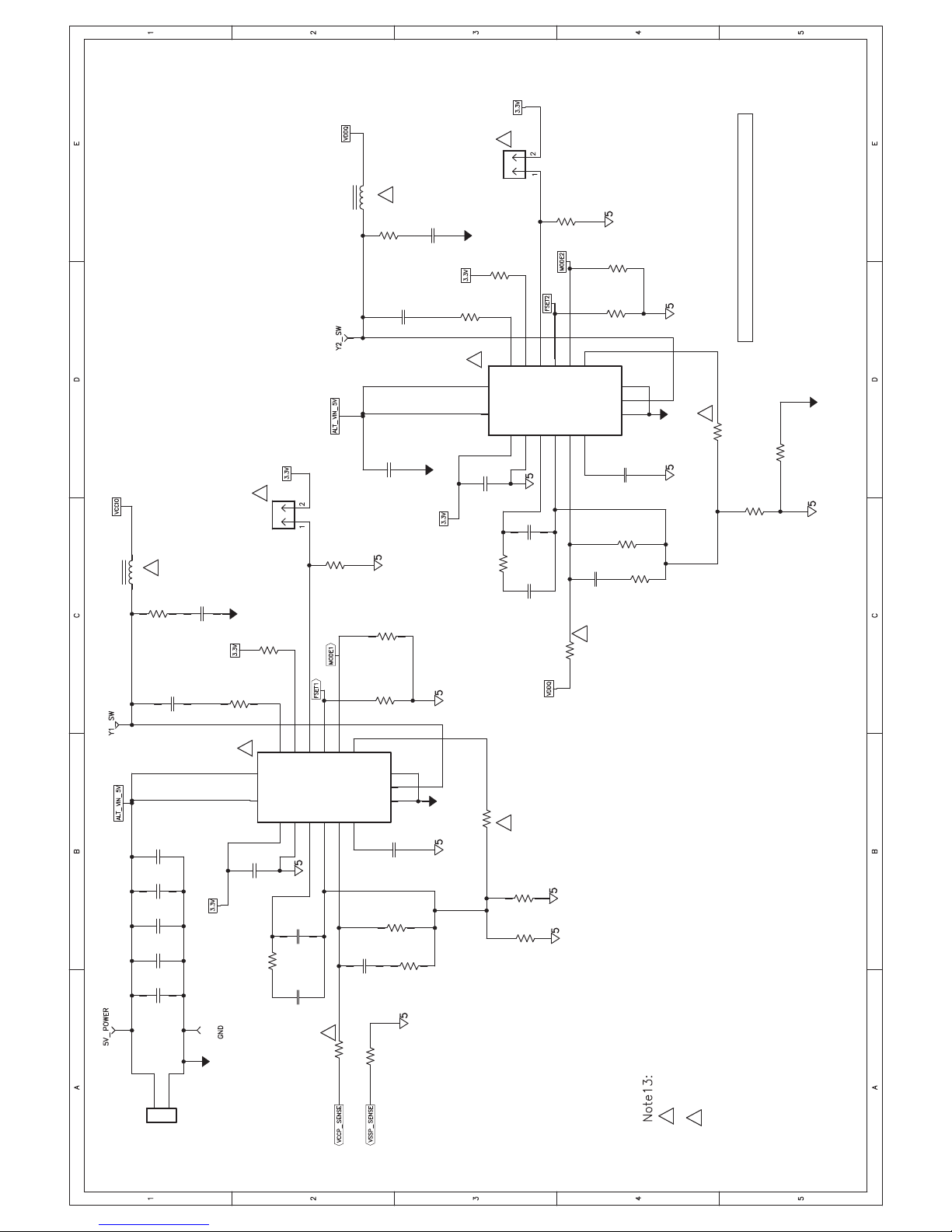
L8
0.42uH
1
R242
2.21
C241
220pF
26
J42
R244
475k
L9
TP112
R246
0.42uH
10.0k
1
R251
C246
R249
2.21
C248
10nF
0
0.22uF
C249
220pF
U22
TPS51318
R254
1
C250
26
J43
R260
10.0k
0
R255
475k
0
R263
R262
10.0k
Optional Solution for VCCIO and VDDQ
14
11
10
13EN12
15
16
VIN
17
VIN
1
VBST
VCCA
2
FSET
PGOOD
GND
COMP6SS
VFB
3
4
MODE
VOUT
5
1uF
C252
100pF
R257 5.62k
C251
680pF
1
IMON
C253
1.8nF
PGND
SW
PGND
C254
R264
9
8
7
2200pF
2.00k
0
R265
1
R266
R267
1.37k
R268
0
TP110
TP109
J41
C239
C238
C237
C236
C235
1
C240
10nF
22uF
22uF
22uF
22uF
2
0.22uF
5V POWER
U21
TP 111
Voltage Input
0
R243
1
16
TPS51318
17
C242
15
VIN
VIN
1
1uF
5.62k
R245
14
VBST
VCCA
2
C244
C243
13EN12
PGOOD
GND
COMP6SS
3
4
100pF
680pF
11
FSET
VFB
5
1
R247
10
IMON
MODE
VOUT
C245
0
R250
R248
PGND
SW
PGND
C247
R252
1.8nF
10.0k
9
8
7
2.00k
2200pF
0
R253
R256
R261
1
R258
3.09k
R259
20.0k
43 to Disable Optional VCCIO and VDDQ
to Enable Optional VCCIO and VDDQ
Not used
J42, J43: Optional VCCIO and VDDQ Enable
1. Jumper shorts on J42, J43
1
2. No Jumper shorts on J42, J
26
Page 65

EVALUATION BOARD/KIT/MODULE (EVM) ADDITIONAL TERMS
Texas Instruments (TI) provides the enclosed Evaluation Board/Kit/Module (EVM) under the following conditions:
The user assumes all responsibility and liability for proper and safe handling of the goods. Further, the user indemnifies TI from all claims
arising from the handling or use of the goods.
Should this evaluation board/kit not meet the specifications indicated in the User’s Guide, the board/kit may be returned within 30 days from
the date of delivery for a full refund. THE FOREGOING LIMITED WARRANTY IS THE EXCLUSIVE WARRANTY MADE BY SELLER TO
BUYER AND IS IN LIEU OF ALL OTHER WARRANTIES, EXPRESSED, IMPLIED, OR STATUTORY, INCLUDING ANY WARRANTY OF
MERCHANTABILITY OR FITNESS FOR ANY PARTICULAR PURPOSE. EXCEPT TO THE EXTENT OF THE INDEMNITY SET FORTH
ABOVE, NEITHER PARTY SHALL BE LIABLE TO THE OTHER FOR ANY INDIRECT, SPECIAL, INCIDENTAL, OR CONSEQUENTIAL
DAMAGES.
Please read the User's Guide and, specifically, the Warnings and Restrictions notice in the User's Guide prior to handling the product. This
notice contains important safety information about temperatures and voltages. For additional information on TI's environmental and/or safety
programs, please visit www.ti.com/esh or contact TI.
No license is granted under any patent right or other intellectual property right of TI covering or relating to any machine, process, or
combination in which such TI products or services might be or are used. TI currently deals with a variety of customers for products, and
therefore our arrangement with the user is not exclusive. TI assumes no liability for applications assistance, customer product design,
software performance, or infringement of patents or services described herein.
REGULATORY COMPLIANCE INFORMATION
As noted in the EVM User’s Guide and/or EVM itself, this EVM and/or accompanying hardware may or may not be subject to the Federal
Communications Commission (FCC) and Industry Canada (IC) rules.
For EVMs not subject to the above rules, this evaluation board/kit/module is intended for use for ENGINEERING DEVELOPMENT,
DEMONSTRATION OR EVALUATION PURPOSES ONLY and is not considered by TI to be a finished end product fit for general consumer
use. It generates, uses, and can radiate radio frequency energy and has not been tested for compliance with the limits of computing
devices pursuant to part 15 of FCC or ICES-003 rules, which are designed to provide reasonable protection against radio frequency
interference. Operation of the equipment may cause interference with radio communications, in which case the user at his own expense will
be required to take whatever measures may be required to correct this interference.
General Statement for EVMs including a radio
User Power/Frequency Use Obligations: This radio is intended for development/professional use only in legally allocated frequency and
power limits. Any use of radio frequencies and/or power availability of this EVM and its development application(s) must comply with local
laws governing radio spectrum allocation and power limits for this evaluation module. It is the user’s sole responsibility to only operate this
radio in legally acceptable frequency space and within legally mandated power limitations. Any exceptions to this are strictly prohibited and
unauthorized by Texas Instruments unless user has obtained appropriate experimental/development licenses from local regulatory
authorities, which is responsibility of user including its acceptable authorization.
For EVMs annotated as FCC – FEDERAL COMMUNICATIONS COMMISSION Part 15 Compliant
Caution
This device complies with part 15 of the FCC Rules. Operation is subject to the following two conditions: (1) This device may not cause
harmful interference, and (2) this device must accept any interference received, including interference that may cause undesired operation.
Changes or modifications not expressly approved by the party responsible for compliance could void the user's authority to operate the
equipment.
FCC Interference Statement for Class A EVM devices
This equipment has been tested and found to comply with the limits for a Class A digital device, pursuant to part 15 of the FCC Rules.
These limits are designed to provide reasonable protection against harmful interference when the equipment is operated in a commercial
environment. This equipment generates, uses, and can radiate radio frequency energy and, if not installed and used in accordance with the
instruction manual, may cause harmful interference to radio communications. Operation of this equipment in a residential area is likely to
cause harmful interference in which case the user will be required to correct the interference at his own expense.
Page 66

FCC Interference Statement for Class B EVM devices
This equipment has been tested and found to comply with the limits for a Class B digital device, pursuant to part 15 of the FCC Rules.
These limits are designed to provide reasonable protection against harmful interference in a residential installation. This equipment
generates, uses and can radiate radio frequency energy and, if not installed and used in accordance with the instructions, may cause
harmful interference to radio communications. However, there is no guarantee that interference will not occur in a particular installation. If
this equipment does cause harmful interference to radio or television reception, which can be determined by turning the equipment off and
on, the user is encouraged to try to correct the interference by one or more of the following measures:
• Reorient or relocate the receiving antenna.
• Increase the separation between the equipment and receiver.
• Connect the equipment into an outlet on a circuit different from that to which the receiver is connected.
• Consult the dealer or an experienced radio/TV technician for help.
For EVMs annotated as IC – INDUSTRY CANADA Compliant
This Class A or B digital apparatus complies with Canadian ICES-003.
Changes or modifications not expressly approved by the party responsible for compliance could void the user’s authority to operate the
equipment.
Concerning EVMs including radio transmitters
This device complies with Industry Canada licence-exempt RSS standard(s). Operation is subject to the following two conditions: (1) this
device may not cause interference, and (2) this device must accept any interference, including interference that may cause undesired
operation of the device.
Concerning EVMs including detachable antennas
Under Industry Canada regulations, this radio transmitter may only operate using an antenna of a type and maximum (or lesser) gain
approved for the transmitter by Industry Canada. To reduce potential radio interference to other users, the antenna type and its gain should
be so chosen that the equivalent isotropically radiated power (e.i.r.p.) is not more than that necessary for successful communication.
This radio transmitter has been approved by Industry Canada to operate with the antenna types listed in the user guide with the maximum
permissible gain and required antenna impedance for each antenna type indicated. Antenna types not included in this list, having a gain
greater than the maximum gain indicated for that type, are strictly prohibited for use with this device.
Cet appareil numérique de la classe A ou B est conforme à la norme NMB-003 du Canada.
Les changements ou les modifications pas expressément approuvés par la partie responsable de la conformité ont pu vider l’autorité de
l'utilisateur pour actionner l'équipement.
Concernant les EVMs avec appareils radio
Le présent appareil est conforme aux CNR d'Industrie Canada applicables aux appareils radio exempts de licence. L'exploitation est
autorisée aux deux conditions suivantes : (1) l'appareil ne doit pas produire de brouillage, et (2) l'utilisateur de l'appareil doit accepter tout
brouillage radioélectrique subi, même si le brouillage est susceptible d'en compromettre le fonctionnement.
Concernant les EVMs avec antennes détachables
Conformément à la réglementation d'Industrie Canada, le présent émetteur radio peut fonctionner avec une antenne d'un type et d'un gain
maximal (ou inférieur) approuvé pour l'émetteur par Industrie Canada. Dans le but de réduire les risques de brouillage radioélectrique à
l'intention des autres utilisateurs, il faut choisir le type d'antenne et son gain de sorte que la puissance isotrope rayonnée équivalente
(p.i.r.e.) ne dépasse pas l'intensité nécessaire à l'établissement d'une communication satisfaisante.
Le présent émetteur radio a été approuvé par Industrie Canada pour fonctionner avec les types d'antenne énumérés dans le manuel
d’usage et ayant un gain admissible maximal et l'impédance requise pour chaque type d'antenne. Les types d'antenne non inclus dans
cette liste, ou dont le gain est supérieur au gain maximal indiqué, sont strictement interdits pour l'exploitation de l'émetteur.
SPACER
SPACER
SPACER
SPACER
SPACER
SPACER
SPACER
SPACER
Page 67

【【Important Notice for Users of this Product in Japan】】
This development kit is NOT certified as Confirming to Technical Regulations of Radio Law of Japan
If you use this product in Japan, you are required by Radio Law of Japan to follow the instructions below with respect to this product:
1. Use this product in a shielded room or any other test facility as defined in the notification #173 issued by Ministry of Internal Affairs and
Communications on March 28, 2006, based on Sub-section 1.1 of Article 6 of the Ministry’s Rule for Enforcement of Radio Law of
Japan,
2. Use this product only after you obtained the license of Test Radio Station as provided in Radio Law of Japan with respect to this
product, or
3. Use of this product only after you obtained the Technical Regulations Conformity Certification as provided in Radio Law of Japan with
respect to this product. Also, please do not transfer this product, unless you give the same notice above to the transferee. Please note
that if you could not follow the instructions above, you will be subject to penalties of Radio Law of Japan.
(address) 24-1, Nishi-Shinjuku 6 chome, Shinjukku-ku, Tokyo, Japan
http://www.tij.co.jp
【ご使用にあたっての注】
本開発キットは技術基準適合証明を受けておりません。
本製品のご使用に際しては、電波法遵守のため、以下のいずれかの措置を取っていただく必要がありますのでご注意ください。
1. 電波法施行規則第6条第1項第1号に基づく平成18年3月28日総務省告示第173号で定められた電波暗室等の試験設備でご使用いただく。
2. 実験局の免許を取得後ご使用いただく。
3. 技術基準適合証明を取得後ご使用いただく。
なお、本製品は、上記の「ご使用にあたっての注意」を譲渡先、移転先に通知しない限り、譲渡、移転できないものとします。
上記を遵守頂けない場合は、電波法の罰則が適用される可能性があることをご留意ください。
日本テキサス・インスツルメンツ株式会社
東京都新宿区西新宿6丁目24番1号
西新宿三井ビル
http://www.tij.co.jp
Texas Instruments Japan Limited
SPACER
SPACER
SPACER
SPACER
SPACER
SPACER
SPACER
SPACER
SPACER
SPACER
SPACER
SPACER
SPACER
SPACER
SPACER
SPACER
Page 68

EVALUATION BOARD/KIT/MODULE (EVM)
WARNINGS, RESTRICTIONS AND DISCLAIMERS
For Feasibility Evaluation Only, in Laboratory/Development Environments. Unless otherwise indicated, this EVM is not a finished
electrical equipment and not intended for consumer use. It is intended solely for use for preliminary feasibility evaluation in
laboratory/development environments by technically qualified electronics experts who are familiar with the dangers and application risks
associated with handling electrical mechanical components, systems and subsystems. It should not be used as all or part of a finished end
product.
Your Sole Responsibility and Risk. You acknowledge, represent and agree that:
1. You have unique knowledge concerning Federal, State and local regulatory requirements (including but not limited to Food and Drug
Administration regulations, if applicable) which relate to your products and which relate to your use (and/or that of your employees,
affiliates, contractors or designees) of the EVM for evaluation, testing and other purposes.
2. You have full and exclusive responsibility to assure the safety and compliance of your products with all such laws and other applicable
regulatory requirements, and also to assure the safety of any activities to be conducted by you and/or your employees, affiliates,
contractors or designees, using the EVM. Further, you are responsible to assure that any interfaces (electronic and/or mechanical)
between the EVM and any human body are designed with suitable isolation and means to safely limit accessible leakage currents to
minimize the risk of electrical shock hazard.
3. You will employ reasonable safeguards to ensure that your use of the EVM will not result in any property damage, injury or death, even
if the EVM should fail to perform as described or expected.
4. You will take care of proper disposal and recycling of the EVM’s electronic components and packing materials.
Certain Instructions. It is important to operate this EVM within TI’s recommended specifications and environmental considerations per the
user guidelines. Exceeding the specified EVM ratings (including but not limited to input and output voltage, current, power, and
environmental ranges) may cause property damage, personal injury or death. If there are questions concerning these ratings please contact
a TI field representative prior to connecting interface electronics including input power and intended loads. Any loads applied outside of the
specified output range may result in unintended and/or inaccurate operation and/or possible permanent damage to the EVM and/or
interface electronics. Please consult the EVM User's Guide prior to connecting any load to the EVM output. If there is uncertainty as to the
load specification, please contact a TI field representative. During normal operation, some circuit components may have case temperatures
greater than 60°C as long as the input and output are maintained at a normal ambient operating temperature. These components include
but are not limited to linear regulators, switching transistors, pass transistors, and current sense resistors which can be identified using the
EVM schematic located in the EVM User's Guide. When placing measurement probes near these devices during normal operation, please
be aware that these devices may be very warm to the touch. As with all electronic evaluation tools, only qualified personnel knowledgeable
in electronic measurement and diagnostics normally found in development environments should use these EVMs.
Agreement to Defend, Indemnify and Hold Harmless. You agree to defend, indemnify and hold TI, its licensors and their representatives
harmless from and against any and all claims, damages, losses, expenses, costs and liabilities (collectively, "Claims") arising out of or in
connection with any use of the EVM that is not in accordance with the terms of the agreement. This obligation shall apply whether Claims
arise under law of tort or contract or any other legal theory, and even if the EVM fails to perform as described or expected.
Safety-Critical or Life-Critical Applications. If you intend to evaluate the components for possible use in safety critical applications (such
as life support) where a failure of the TI product would reasonably be expected to cause severe personal injury or death, such as devices
which are classified as FDA Class III or similar classification, then you must specifically notify TI of such intent and enter into a separate
Assurance and Indemnity Agreement.
Mailing Address: Texas Instruments, Post Office Box 655303, Dallas, Texas 75265
Copyright © 2012, Texas Instruments Incorporated
Page 69

EVALUATION BOARD/KIT/MODULE (EVM) ADDITIONAL TERMS
Texas Instruments (TI) provides the enclosed Evaluation Board/Kit/Module (EVM) under the following conditions:
The user assumes all responsibility and liability for proper and safe handling of the goods. Further, the user indemnifies TI from all claims
arising from the handling or use of the goods.
Should this evaluation board/kit not meet the specifications indicated in the User’s Guide, the board/kit may be returned within 30 days from
the date of delivery for a full refund. THE FOREGOING LIMITED WARRANTY IS THE EXCLUSIVE WARRANTY MADE BY SELLER TO
BUYER AND IS IN LIEU OF ALL OTHER WARRANTIES, EXPRESSED, IMPLIED, OR STATUTORY, INCLUDING ANY WARRANTY OF
MERCHANTABILITY OR FITNESS FOR ANY PARTICULAR PURPOSE. EXCEPT TO THE EXTENT OF THE INDEMNITY SET FORTH
ABOVE, NEITHER PARTY SHALL BE LIABLE TO THE OTHER FOR ANY INDIRECT, SPECIAL, INCIDENTAL, OR CONSEQUENTIAL
DAMAGES.
Please read the User's Guide and, specifically, the Warnings and Restrictions notice in the User's Guide prior to handling the product. This
notice contains important safety information about temperatures and voltages. For additional information on TI's environmental and/or safety
programs, please visit www.ti.com/esh or contact TI.
No license is granted under any patent right or other intellectual property right of TI covering or relating to any machine, process, or
combination in which such TI products or services might be or are used. TI currently deals with a variety of customers for products, and
therefore our arrangement with the user is not exclusive. TI assumes no liability for applications assistance, customer product design,
software performance, or infringement of patents or services described herein.
REGULATORY COMPLIANCE INFORMATION
As noted in the EVM User’s Guide and/or EVM itself, this EVM and/or accompanying hardware may or may not be subject to the Federal
Communications Commission (FCC) and Industry Canada (IC) rules.
For EVMs not subject to the above rules, this evaluation board/kit/module is intended for use for ENGINEERING DEVELOPMENT,
DEMONSTRATION OR EVALUATION PURPOSES ONLY and is not considered by TI to be a finished end product fit for general consumer
use. It generates, uses, and can radiate radio frequency energy and has not been tested for compliance with the limits of computing
devices pursuant to part 15 of FCC or ICES-003 rules, which are designed to provide reasonable protection against radio frequency
interference. Operation of the equipment may cause interference with radio communications, in which case the user at his own expense will
be required to take whatever measures may be required to correct this interference.
General Statement for EVMs including a radio
User Power/Frequency Use Obligations: This radio is intended for development/professional use only in legally allocated frequency and
power limits. Any use of radio frequencies and/or power availability of this EVM and its development application(s) must comply with local
laws governing radio spectrum allocation and power limits for this evaluation module. It is the user’s sole responsibility to only operate this
radio in legally acceptable frequency space and within legally mandated power limitations. Any exceptions to this are strictly prohibited and
unauthorized by Texas Instruments unless user has obtained appropriate experimental/development licenses from local regulatory
authorities, which is responsibility of user including its acceptable authorization.
For EVMs annotated as FCC – FEDERAL COMMUNICATIONS COMMISSION Part 15 Compliant
Caution
This device complies with part 15 of the FCC Rules. Operation is subject to the following two conditions: (1) This device may not cause
harmful interference, and (2) this device must accept any interference received, including interference that may cause undesired operation.
Changes or modifications not expressly approved by the party responsible for compliance could void the user's authority to operate the
equipment.
FCC Interference Statement for Class A EVM devices
This equipment has been tested and found to comply with the limits for a Class A digital device, pursuant to part 15 of the FCC Rules.
These limits are designed to provide reasonable protection against harmful interference when the equipment is operated in a commercial
environment. This equipment generates, uses, and can radiate radio frequency energy and, if not installed and used in accordance with the
instruction manual, may cause harmful interference to radio communications. Operation of this equipment in a residential area is likely to
cause harmful interference in which case the user will be required to correct the interference at his own expense.
Page 70

FCC Interference Statement for Class B EVM devices
This equipment has been tested and found to comply with the limits for a Class B digital device, pursuant to part 15 of the FCC Rules.
These limits are designed to provide reasonable protection against harmful interference in a residential installation. This equipment
generates, uses and can radiate radio frequency energy and, if not installed and used in accordance with the instructions, may cause
harmful interference to radio communications. However, there is no guarantee that interference will not occur in a particular installation. If
this equipment does cause harmful interference to radio or television reception, which can be determined by turning the equipment off and
on, the user is encouraged to try to correct the interference by one or more of the following measures:
• Reorient or relocate the receiving antenna.
• Increase the separation between the equipment and receiver.
• Connect the equipment into an outlet on a circuit different from that to which the receiver is connected.
• Consult the dealer or an experienced radio/TV technician for help.
For EVMs annotated as IC – INDUSTRY CANADA Compliant
This Class A or B digital apparatus complies with Canadian ICES-003.
Changes or modifications not expressly approved by the party responsible for compliance could void the user’s authority to operate the
equipment.
Concerning EVMs including radio transmitters
This device complies with Industry Canada licence-exempt RSS standard(s). Operation is subject to the following two conditions: (1) this
device may not cause interference, and (2) this device must accept any interference, including interference that may cause undesired
operation of the device.
Concerning EVMs including detachable antennas
Under Industry Canada regulations, this radio transmitter may only operate using an antenna of a type and maximum (or lesser) gain
approved for the transmitter by Industry Canada. To reduce potential radio interference to other users, the antenna type and its gain should
be so chosen that the equivalent isotropically radiated power (e.i.r.p.) is not more than that necessary for successful communication.
This radio transmitter has been approved by Industry Canada to operate with the antenna types listed in the user guide with the maximum
permissible gain and required antenna impedance for each antenna type indicated. Antenna types not included in this list, having a gain
greater than the maximum gain indicated for that type, are strictly prohibited for use with this device.
Cet appareil numérique de la classe A ou B est conforme à la norme NMB-003 du Canada.
Les changements ou les modifications pas expressément approuvés par la partie responsable de la conformité ont pu vider l’autorité de
l'utilisateur pour actionner l'équipement.
Concernant les EVMs avec appareils radio
Le présent appareil est conforme aux CNR d'Industrie Canada applicables aux appareils radio exempts de licence. L'exploitation est
autorisée aux deux conditions suivantes : (1) l'appareil ne doit pas produire de brouillage, et (2) l'utilisateur de l'appareil doit accepter tout
brouillage radioélectrique subi, même si le brouillage est susceptible d'en compromettre le fonctionnement.
Concernant les EVMs avec antennes détachables
Conformément à la réglementation d'Industrie Canada, le présent émetteur radio peut fonctionner avec une antenne d'un type et d'un gain
maximal (ou inférieur) approuvé pour l'émetteur par Industrie Canada. Dans le but de réduire les risques de brouillage radioélectrique à
l'intention des autres utilisateurs, il faut choisir le type d'antenne et son gain de sorte que la puissance isotrope rayonnée équivalente
(p.i.r.e.) ne dépasse pas l'intensité nécessaire à l'établissement d'une communication satisfaisante.
Le présent émetteur radio a été approuvé par Industrie Canada pour fonctionner avec les types d'antenne énumérés dans le manuel
d’usage et ayant un gain admissible maximal et l'impédance requise pour chaque type d'antenne. Les types d'antenne non inclus dans
cette liste, ou dont le gain est supérieur au gain maximal indiqué, sont strictement interdits pour l'exploitation de l'émetteur.
SPACER
SPACER
SPACER
SPACER
SPACER
SPACER
SPACER
SPACER
Page 71

【【Important Notice for Users of this Product in Japan】】
This development kit is NOT certified as Confirming to Technical Regulations of Radio Law of Japan
If you use this product in Japan, you are required by Radio Law of Japan to follow the instructions below with respect to this product:
1. Use this product in a shielded room or any other test facility as defined in the notification #173 issued by Ministry of Internal Affairs and
Communications on March 28, 2006, based on Sub-section 1.1 of Article 6 of the Ministry’s Rule for Enforcement of Radio Law of
Japan,
2. Use this product only after you obtained the license of Test Radio Station as provided in Radio Law of Japan with respect to this
product, or
3. Use of this product only after you obtained the Technical Regulations Conformity Certification as provided in Radio Law of Japan with
respect to this product. Also, please do not transfer this product, unless you give the same notice above to the transferee. Please note
that if you could not follow the instructions above, you will be subject to penalties of Radio Law of Japan.
(address) 24-1, Nishi-Shinjuku 6 chome, Shinjuku-ku, Tokyo, Japan
http://www.tij.co.jp
【ご使用にあたっての注】
本開発キットは技術基準適合証明を受けておりません。
本製品のご使用に際しては、電波法遵守のため、以下のいずれかの措置を取っていただく必要がありますのでご注意ください。
1. 電波法施行規則第6条第1項第1号に基づく平成18年3月28日総務省告示第173号で定められた電波暗室等の試験設備でご使用いただく。
2. 実験局の免許を取得後ご使用いただく。
3. 技術基準適合証明を取得後ご使用いただく。
なお、本製品は、上記の「ご使用にあたっての注意」を譲渡先、移転先に通知しない限り、譲渡、移転できないものとします。
上記を遵守頂けない場合は、電波法の罰則が適用される可能性があることをご留意ください。
日本テキサス・インスツルメンツ株式会社
東京都新宿区西新宿6丁目24番1号
西新宿三井ビル
http://www.tij.co.jp
Texas Instruments Japan Limited
SPACER
SPACER
SPACER
SPACER
SPACER
SPACER
SPACER
SPACER
SPACER
SPACER
SPACER
SPACER
SPACER
SPACER
SPACER
SPACER
Page 72

EVALUATION BOARD/KIT/MODULE (EVM)
WARNINGS, RESTRICTIONS AND DISCLAIMERS
For Feasibility Evaluation Only, in Laboratory/Development Environments. Unless otherwise indicated, this EVM is not a finished
electrical equipment and not intended for consumer use. It is intended solely for use for preliminary feasibility evaluation in
laboratory/development environments by technically qualified electronics experts who are familiar with the dangers and application risks
associated with handling electrical mechanical components, systems and subsystems. It should not be used as all or part of a finished end
product.
Your Sole Responsibility and Risk. You acknowledge, represent and agree that:
1. You have unique knowledge concerning Federal, State and local regulatory requirements (including but not limited to Food and Drug
Administration regulations, if applicable) which relate to your products and which relate to your use (and/or that of your employees,
affiliates, contractors or designees) of the EVM for evaluation, testing and other purposes.
2. You have full and exclusive responsibility to assure the safety and compliance of your products with all such laws and other applicable
regulatory requirements, and also to assure the safety of any activities to be conducted by you and/or your employees, affiliates,
contractors or designees, using the EVM. Further, you are responsible to assure that any interfaces (electronic and/or mechanical)
between the EVM and any human body are designed with suitable isolation and means to safely limit accessible leakage currents to
minimize the risk of electrical shock hazard.
3. You will employ reasonable safeguards to ensure that your use of the EVM will not result in any property damage, injury or death, even
if the EVM should fail to perform as described or expected.
4. You will take care of proper disposal and recycling of the EVM’s electronic components and packing materials.
Certain Instructions. It is important to operate this EVM within TI’s recommended specifications and environmental considerations per the
user guidelines. Exceeding the specified EVM ratings (including but not limited to input and output voltage, current, power, and
environmental ranges) may cause property damage, personal injury or death. If there are questions concerning these ratings please contact
a TI field representative prior to connecting interface electronics including input power and intended loads. Any loads applied outside of the
specified output range may result in unintended and/or inaccurate operation and/or possible permanent damage to the EVM and/or
interface electronics. Please consult the EVM User's Guide prior to connecting any load to the EVM output. If there is uncertainty as to the
load specification, please contact a TI field representative. During normal operation, some circuit components may have case temperatures
greater than 60°C as long as the input and output are maintained at a normal ambient operating temperature. These components include
but are not limited to linear regulators, switching transistors, pass transistors, and current sense resistors which can be identified using the
EVM schematic located in the EVM User's Guide. When placing measurement probes near these devices during normal operation, please
be aware that these devices may be very warm to the touch. As with all electronic evaluation tools, only qualified personnel knowledgeable
in electronic measurement and diagnostics normally found in development environments should use these EVMs.
Agreement to Defend, Indemnify and Hold Harmless. You agree to defend, indemnify and hold TI, its licensors and their representatives
harmless from and against any and all claims, damages, losses, expenses, costs and liabilities (collectively, "Claims") arising out of or in
connection with any use of the EVM that is not in accordance with the terms of the agreement. This obligation shall apply whether Claims
arise under law of tort or contract or any other legal theory, and even if the EVM fails to perform as described or expected.
Safety-Critical or Life-Critical Applications. If you intend to evaluate the components for possible use in safety critical applications (such
as life support) where a failure of the TI product would reasonably be expected to cause severe personal injury or death, such as devices
which are classified as FDA Class III or similar classification, then you must specifically notify TI of such intent and enter into a separate
Assurance and Indemnity Agreement.
Mailing Address: Texas Instruments, Post Office Box 655303, Dallas, Texas 75265
Copyright © 2012, Texas Instruments Incorporated
Page 73

IMPORTANT NOTICE FOR TI REFERENCE DESIGNS
Texas Instruments Incorporated ("TI") reference designs are solely intended to assist designers (“Buyers”) who are developing systems that
incorporate TI semiconductor products (also referred to herein as “components”). Buyer understands and agrees that Buyer remains
responsible for using its independent analysis, evaluation and judgment in designing Buyer’s systems and products.
TI reference designs have been created using standard laboratory conditions and engineering practices. TI has not conducted any
testing other than that specifically described in the published documentation for a particular reference design. TI may make
corrections, enhancements, improvements and other changes to its reference designs.
Buyers are authorized to use TI reference designs with the TI component(s) identified in each particular reference design and to modify the
reference design in the development of their end products. HOWEVER, NO OTHER LICENSE, EXPRESS OR IMPLIED, BY ESTOPPEL
OR OTHERWISE TO ANY OTHER TI INTELLECTUAL PROPERTY RIGHT, AND NO LICENSE TO ANY THIRD PARTY TECHNOLOGY
OR INTELLECTUAL PROPERTY RIGHT, IS GRANTED HEREIN, including but not limited to any patent right, copyright, mask work right,
or other intellectual property right relating to any combination, machine, or process in which TI components or services are used.
Information published by TI regarding third-party products or services does not constitute a license to use such products or services, or a
warranty or endorsement thereof. Use of such information may require a license from a third party under the patents or other intellectual
property of the third party, or a license from TI under the patents or other intellectual property of TI.
TI REFERENCE DESIGNS ARE PROVIDED "AS IS". TI MAKES NO WARRANTIES OR REPRESENTATIONS WITH REGARD TO THE
REFERENCE DESIGNS OR USE OF THE REFERENCE DESIGNS, EXPRESS, IMPLIED OR STATUTORY, INCLUDING ACCURACY OR
COMPLETENESS. TI DISCLAIMS ANY WARRANTY OF TITLE AND ANY IMPLIED WARRANTIES OF MERCHANTABILITY, FITNESS
FOR A PARTICULAR PURPOSE, QUIET ENJOYMENT, QUIET POSSESSION, AND NON-INFRINGEMENT OF ANY THIRD PARTY
INTELLECTUAL PROPERTY RIGHTS WITH REGARD TO TI REFERENCE DESIGNS OR USE THEREOF. TI SHALL NOT BE LIABLE
FOR AND SHALL NOT DEFEND OR INDEMNIFY BUYERS AGAINST ANY THIRD PARTY INFRINGEMENT CLAIM THAT RELATES TO
OR IS BASED ON A COMBINATION OF COMPONENTS PROVIDED IN A TI REFERENCE DESIGN. IN NO EVENT SHALL TI BE
LIABLE FOR ANY ACTUAL, SPECIAL, INCIDENTAL, CONSEQUENTIAL OR INDIRECT DAMAGES, HOWEVER CAUSED, ON ANY
THEORY OF LIABILITY AND WHETHER OR NOT TI HAS BEEN ADVISED OF THE POSSIBILITY OF SUCH DAMAGES, ARISING IN
ANY WAY OUT OF TI REFERENCE DESIGNS OR BUYER’S USE OF TI REFERENCE DESIGNS.
TI reserves the right to make corrections, enhancements, improvements and other changes to its semiconductor products and services per
JESD46, latest issue, and to discontinue any product or service per JESD48, latest issue. Buyers should obtain the latest relevant
information before placing orders and should verify that such information is current and complete. All semiconductor products are sold
subject to TI’s terms and conditions of sale supplied at the time of order acknowledgment.
TI warrants performance of its components to the specifications applicable at the time of sale, in accordance with the warranty in TI’s terms
and conditions of sale of semiconductor products. Testing and other quality control techniques for TI components are used to the extent TI
deems necessary to support this warranty. Except where mandated by applicable law, testing of all parameters of each component is not
necessarily performed.
TI assumes no liability for applications assistance or the design of Buyers’ products. Buyers are responsible for their products and
applications using TI components. To minimize the risks associated with Buyers’ products and applications, Buyers should provide
adequate design and operating safeguards.
Reproduction of significant portions of TI information in TI data books, data sheets or reference designs is permissible only if reproduction is
without alteration and is accompanied by all associated warranties, conditions, limitations, and notices. TI is not responsible or liable for
such altered documentation. Information of third parties may be subject to additional restrictions.
Buyer acknowledges and agrees that it is solely responsible for compliance with all legal, regulatory and safety-related requirements
concerning its products, and any use of TI components in its applications, notwithstanding any applications-related information or support
that may be provided by TI. Buyer represents and agrees that it has all the necessary expertise to create and implement safeguards that
anticipate dangerous failures, monitor failures and their consequences, lessen the likelihood of dangerous failures and take appropriate
remedial actions. Buyer will fully indemnify TI and its representatives against any damages arising out of the use of any TI components in
Buyer’s safety-critical applications.
In some cases, TI components may be promoted specifically to facilitate safety-related applications. With such components, TI’s goal is to
help enable customers to design and create their own end-product solutions that meet applicable functional safety standards and
requirements. Nonetheless, such components are subject to these terms.
No TI components are authorized for use in FDA Class III (or similar life-critical medical equipment) unless authorized officers of the parties
have executed an agreement specifically governing such use.
Only those TI components that TI has specifically designated as military grade or “enhanced plastic” are designed and intended for use in
military/aerospace applications or environments. Buyer acknowledges and agrees that any military or aerospace use of TI components that
have not been so designated is solely at Buyer's risk, and Buyer is solely responsible for compliance with all legal and regulatory
requirements in connection with such use.
TI has specifically designated certain components as meeting ISO/TS16949 requirements, mainly for automotive use. In any case of use of
non-designated products, TI will not be responsible for any failure to meet ISO/TS16949.
Mailing Address: Texas Instruments, Post Office Box 655303, Dallas, Texas 75265
Copyright © 2013, Texas Instruments Incorporated
 Loading...