

Page 1
www.ti.com
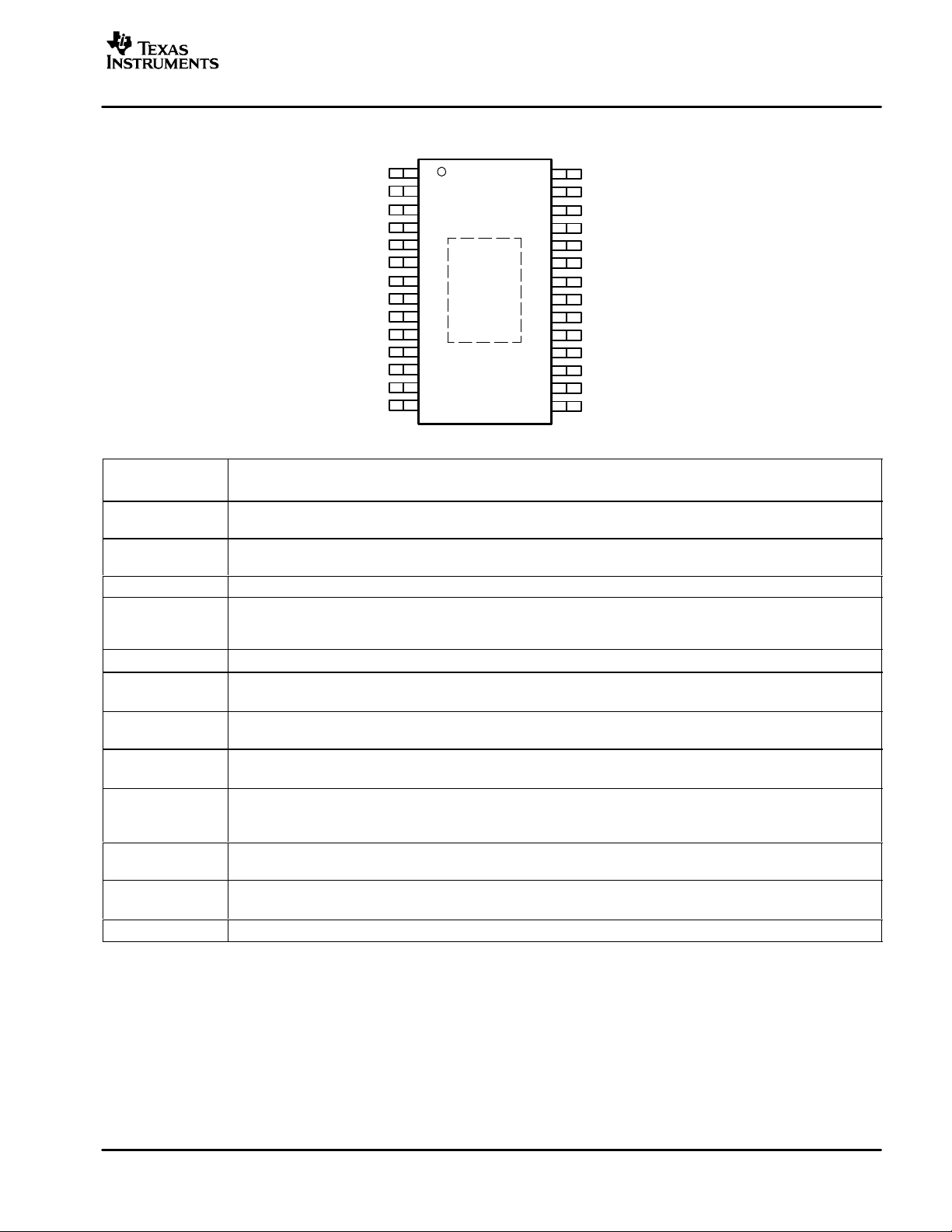
6,4 mm X 9,7 mm
SLVS420B − MARCH 2002 − R EVISED FEBRUARY 2005
4-V TO 6-V INPUT, 8-A OUTPUT SYNCHRONOUS BUCK PWM
SWITCHER WITH INTEGRATED FETS (SWIFT™)
TPS54810
FEATURES
D 30-mΩ MOSFET Switches for High Efficiency
at 8-A Continuous Output
D 0.9-V to 3.3-V Adjustable Output Voltage
Range With 1% Accuracy
D Externally Compensated
D Fast Transient Response
D Wide PWM Frequency:
Fixed 350 kHz, 550 kHz or
Adjustable 280 kHz to 700 kHz
D Load Protected by Peak Current Limit and
Thermal Shutdown
D Integrated Solution Reduces Board Area and
Total Cost
APPLICATIONS
D Low-Voltage, High-Density Systems With
Power Distributed at 5 V
D Point of Load Regulation for High
Performance DSPs, FPGAs, ASICs and
Microprocessors
D Broadband, Networking, and Optical
Communications Infrastructure
D Portable Computing/Notebook PCs
DESCRIPTION
As a member of the SWIFT™ family of dc/dc regulators,
the TPS54810 low-input voltage high-output current
synchronous buck PWM converter integrates all
required active components. Included on the substrate
with the listed features are a true, high performance,
voltage error amplifier that enables maximum
performance under transient conditions and flexibility in
choosing the output filter L and C components; an
under-voltage-lockout circuit to prevent start-up until
the input voltage reaches 3.8 V; an internally or
externally set slow-start circuit to limit in-rush currents;
and a power good output useful for processor/logic
reset, fault signaling, and supply sequencing.
The TPS54810 is available in a thermally enhanced
28-pin TSSOP (PWP) PowerPAD™ package, which
eliminates bulky heatsinks. TI provides evaluation
modules and the SWIFT™ designer software tool to aid
in quickly achieving high-performance power supply
designs to meet aggressive equipment development
cycles.
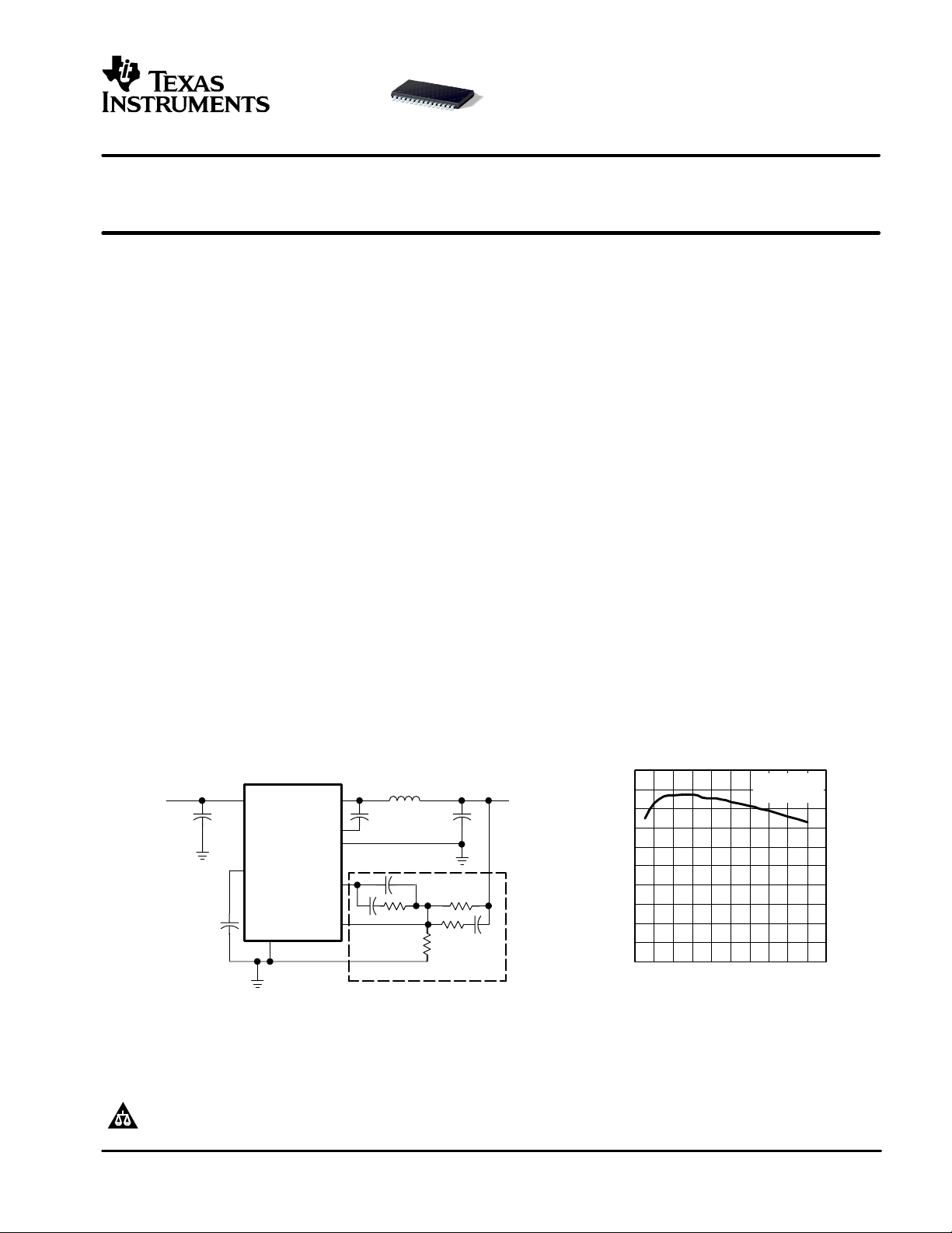
SIMPLIFIED SCHEMATIC
Input
Please be aware that an important notice concerning availability, standard warranty, and use in critical applications of Texas Instruments
semiconductor products and disclaimers thereto appears at the end of this data sheet.
PowerPAD and SWIFT are trademarks of Texas Instruments.
PRODUCTION DATA information is current as of publication date. Products
conform to specifications per the terms of Texas Instruments standard warranty.
Production processing does not necessarily include testing of all parameters.
VIN PH
TPS54810
BOOT
PGND
VBIAS
VSENSE
COMP
VSENSE
AGND
Compensation Network
Output
100
Efficiency − %
EFFICIENCY AT 700 HZ
95
90
85
80
75
70
65
60
55
50
012345678910
IL − Load Current − A
Copyright © 2002, Texas Instruments Incorporated
VI = 5 V
VO = 3.3 V
Page 2
TPS54810
Sink current, I
S
SLVS420B − MARCH 2002 − R EVISED FEBRUARY 2005
These devices have limited built-in ESD protection. The leads should be shorted together or the device placed in conductive foam during
storage or handling to prevent electrostatic damage to the MOS gates.
ORDERING INFORMATION
www.ti.com
T
A
−40°C to 85°C 0.9 V to 3.3 V PLASTIC HTSSOP (PWP)
(1)
The PWP package is also available taped and reeled. Add an R suffix to the device type (i.e., TPS54810PWPR). See the application section
OUTPUT VOLTAGE PACKAGE PART NUMBER
(1)
TPS54810PWP
of the data sheet for PowerPAD™ drawing and layout information.
(2)
For the most current package and ordering information, see the Package Option Addendum at the end of this document, or see the TI website
at www.ti.com.
ABSOLUTE MAXIMUM RATINGS
over operating free-air temperature range unless otherwise noted
VIN, SS/ENA, SYNC −0.3 to 7
Input voltage range, V
I
RT −0.3 to 6
VSENSE −0.3 to 4
BOOT −0.3 to 17
Output voltage range, V
Source current, I
O
O
VBIAS, COMP, PWRGD −0.3 to 7
PH −0.6 to 10
PH Internally Limited
COMP, VBIAS 6 mA
PH 12 A
Sink current, I
S
COMP 6
SS/ENA, PWRGD 10
Voltage differential AGND to PGND ±0.3 V
Operating virtual junction temperature range, T
Storage temperature, T
stg
J
Lead temperature 1,6 mm (1/16 inch) from case for 10 seconds 300 °C
(1)
Stresses beyond those listed under “absolute maximum ratings” may cause permanent damage to the device. These are stress ratings only, and
functional operation of the device at these or any other conditions beyond those indicated under “recommended operating conditions” is not
implied. Exposure to absolute-maximum-rated conditions for extended periods may affect device reliability.
(1)
TPS54810 UNIT
−40 to 125 °C
−65 to 150 °C
V
V
mA
RECOMMENDED OPERATING CONDITIONS
Input voltage range, V
Operating junction temperature, T
DISSIPATION RATINGS
28-Pin PWP with solder 18.2 °C/W 5.49 W
28-Pin PWP without solder 40.5 °C/W 2.48 W 1.36 W 0.99 W
(1)
For more information on the PWP package, refer to TI technical brief, literature number SLMA002.
(2)
Test Board Conditions:
1. 3” x 3”, 4 layers, thickness: 0.062”
2. 1.5 oz. copper traces located on the top of the PCB
3. 1.5 oz. copper ground plane on the bottom of the PCB
4. 0.5 oz. copper ground planes on the 2 internal layers
5. 12 thermal vias (see “Recommended Land Pattern” in applications section of this data sheet)
(3)
Maximum power dissipation may be limited by over current protection.
2
I
PACKAGE
J
(1) (2)
THERMAL IMPEDANCE
JUNCTION-TO-AMBIENT
TA ≤ 25°C
POWER RATING
MIN NOM MAX UNIT
4 6 V
−40 125 °C
TA = 70°C
POWER RATING
(2)
3.02 W 2.20 W
TA = 85°C
POWER RATING
Page 3
www.ti.com
(1) (3)
(1) (3)
Externally set free running frequency range
kHz
ELECTRICAL CHARACTERISTICS
TJ = −40°C to 125°C, VI = 4 V to 6 V unless otherwise noted
PARAMETER TEST CONDITIONS MIN TYP MAX UNIT
SUPPLY VOLTAGE, VIN
Input voltage range, VIN 4.0 6.0 V
I
(Q)
UNDER VOLTAGE LOCK OUT
BIAS VOLTAGE
CUMULATIVE REFERENCE
V
REGULATION
OSCILLATOR
(1)
(2)
(3)
Quiescent current
Start threshold voltage, UVLO 3.8 3.85 V
Stop threshold voltage, UVLO 3.40 3.50 V
Hysteresis voltage, UVLO 0.14 0.16 V
Rising and falling edge deglitch, UVLO
(1)
Output voltage, VBIAS I
Output current, VBIAS
Accuracy 0.882 0.891 0.900 V
ref
(2)
Line regulation
Load regulation
Internally set—free running frequency range
Externally set—free running frequency range
High level threshold, SYNC 2.5 V
Low level threshold, SYNC 0.8 V
Pulse duration, external sychronization, SYNC
Frequency range, SYNC
Ramp valley
(1)
Ramp amplitude (peak-to-peak)
Minimum controllable on time
Maximum duty cycle
(1)
(1)
(1)
(1)
(1)
Specified by design
Static resistive loads only
Specified by the circuit used in Figure 9
TPS54810
SLVS420B − MARCH 2002 − R EVISED FEBRUARY 2005
fs = 350 kHz, SYNC ≤ 0.8 V, RT open,
PH pin open
fs = 550 kHz, SYNC ≥ 2.5 V, RT open,
PH pin open
Shutdown, SS/ENA = 0 V 1.0 1.4
= 0 2.70 2.80 2.90 V
(VBIAS)
IL = 4 A, fs = 350 kHz, TJ = 85°C 0.04
IL = 4 A, fs = 550 kHz, TJ = 85°C 0.04
IL = 0 A to 8 A, fs = 350 kHz, TJ = 85°C 0.03
IL = 0 A to 8 A, fs = 550 kHz, TJ = 85°C 0.03
SYNC ≤ 0.8 V, RT open 280 350 420
SYNC ≥ 2.5 V, RT open 440 550 660
RT = 180 kΩ (1% resistor to AGND) 252 280 308
RT = 100 kΩ (1% resistor to AGND) 460 500 540
RT = 68 kΩ (1% resistor to AGND) 663 700 762
50 ns
330 700 kHz
90%
11 15.8
16 23.5
2.5 µs
100 µA
0.75 V
1 V
200 ns
mA
%/V
%/A
kHz
kHz
3
Page 4
TPS54810
SLVS420B − MARCH 2002 − R EVISED FEBRUARY 2005
www.ti.com
ELECTRICAL CHARACTERISTICS CONTINUED
TJ = −40°C to 125°C, VI = 4 V to 6 V unless otherwise noted
PARAMETER TEST CONDITIONS MIN TYP MAX UNIT
ERROR AMPLIFIER
Error amplifier open loop voltage gain 1 kΩ COMP to AGND
Error amplifier unity gain bandwidth Parallel 10 kΩ, 160 pF COMP to AGND
Error amplifier common mode input voltage
range
Powered by internal LDO
Input bias current, VSENSE VSENSE = V
Output voltage slew rate (symmetric), COMP 1.0 1.4 V/µs
PWM COMPARATOR
PWM comparator propagation delay time, PWM
comparator input to PH pin (excluding dead-
10-mV overdrive
time)
SLOW-START/ENABLE
Enable threshold voltage, SS/ENA 0.82 1.20 1.40 V
Enable hysteresis voltage, SS/ENA
Falling edge deglitch, SS/ENA
(1)
(1)
Internal slow-start time 2.6 3.35 4.1 ms
Charge current, SS/ENA SS/ENA = 0V 3 5 8 µA
Discharge current, SS/ENA SS/ENA = 1.3 V, VI = 1.5 V 1.5 2.3 4.0 mA
POWER GOOD
Power good threshold voltage VSENSE falling 90 %V
Power good hysteresis voltage
Power good falling edge deglitch
Output saturation voltage, PWRGD I
Leakage current, PWRGD V
(1)
(1)
= 2.5 mA 0.18 0.3 V
(sink)
= 3.6 V 1 µA
I
CURRENT LIMIT
(1)
V
Current limit
I
V
I
= 4.5 V
= 6 V
, output shorted 9 11
(1)
, output shorted 10 12
Current limit leading edge blanking time 100 ns
Current limit total response time 200 ns
THERMAL SHUTDOWN
Thermal shutdown trip point
Thermal shutdown hysteresis
(1)
(1)
OUTPUT POWER MOSFETS
(2)
r
DS(on)
(1)
(2)
Power MOSFET switches
Specified by design
Matched MOSFETs, low-side r
production tested, high-side r
DS(on)
VI = 6 V
VI = 4.5 V
(2)
DS(on)
(1)
(1)
ref
(1)
production tested.
90 110 dB
(1)
3 5 MHz
0 VBIAS V
60 250 nA
70 85 ns
0.03 V
2.5 µs
3 %V
35 µs
135 150 165 _C
10 _C
26 47
30 60
ref
ref
A
mΩ
4
Page 5
www.ti.com
TPS54810
SLVS420B − MARCH 2002 − R EVISED FEBRUARY 2005
PWP PACKAGE
(TOP VIEW)
AGND
VSENSE
COMP
PWRGD
BOOT
PH
PH
PH
PH
PH
PH
PH
PH
PH
1
2
3
4
5
6
7
8
9
10
11
12
13
14
THERMAL
PAD
28
27
26
25
24
23
22
21
20
19
18
17
16
15
RT
SYNC
SS/ENA
VBIAS
VIN
VIN
VIN
VIN
VIN
PGND
PGND
PGND
PGND
PGND
Terminal Functions
TERMINAL
NAME NO.
AGND 1 Analog ground. Return for compensation network/output divider, slow-start capacitor, VBIAS capacitor, RT resistor and
SYNC pin. Connect PowerPAD to AGND.
BOOT 5 Bootstrap input. 0.022-µF to 0.1-µF low-ESR capacitor connected from BOOT to PH generates floating drive for the
high-side FET driver.
COMP 3 Error amplifier output. Connect frequency compensation network from COMP to VSENSE.
PGND 15−19 Power ground. High current return for the low-side driver and power MOSFET. Connect PGND with large copper areas
to the input and output supply returns, and negative terminals of the input and output capacitors. A single point
connection to AGND is recommended.
PH 6−14 Phase input/output. Junction of the internal high-side and low-side power MOSFETs, and output inductor.
PWRGD 4 Power good open drain output. High-Z when VSENSE ≥ 90% V
when SS/ENA is low or the internal shutdown signal is active.
RT 28 Frequency setting resistor input. Connect a resistor from RT to AGND to set the switching frequency. When using the
SYNC pin, set the RT value for a frequency at or slightly lower than the external oscillator frequency.
SS/ENA 26 Slow-start/enable input/output. Dual function pin which provides logic input to enable/disable device operation and
capacitor input to externally set the start-up time.
SYNC 27 Synchronization input. Dual function pin which provides logic input to synchronize to an external oscillator or pin select
between two internally set switching frequencies. When used to synchronize to an external signal, a resistor must be
connected to the RT pin.
VBIAS 25 Internal bias regulator output. Supplies regulated voltage to internal circuitry. Bypass VBIAS pin to AGND pin with a
high quality, low-ESR 0.1-µF to 1.0-µF ceramic capacitor.
VIN
VSENSE 2 Error amplifier inverting input. Connect to output voltage through compensation network/output divider.
20−24 Input supply for the power MOSFET switches and internal bias regulator. Bypass VIN pins to PGND pins close to
device package with a high quality, low-ESR 10-µF ceramic capacitor.
DESCRIPTION
ref
, otherwise PWRGD is low. Note that output is low
5
Page 6
TPS54810
SLVS420B − MARCH 2002 − R EVISED FEBRUARY 2005
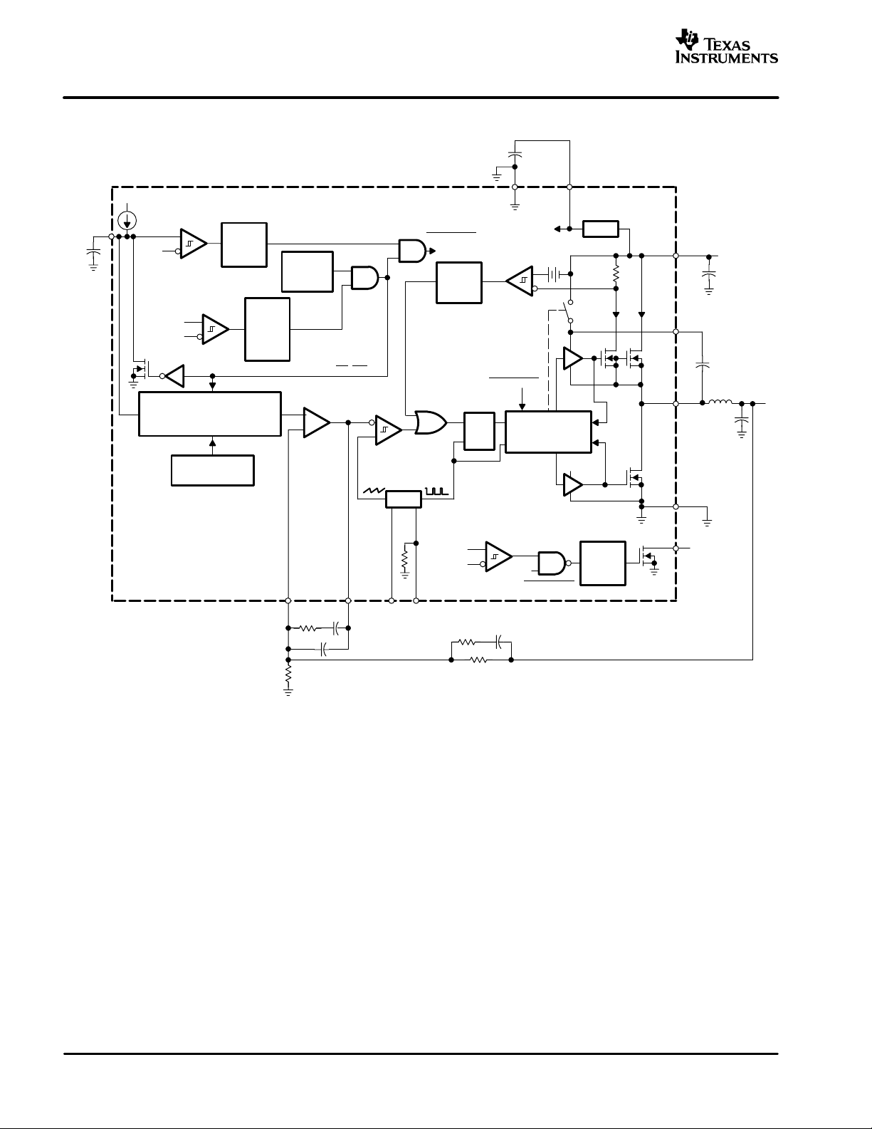
FUNCTIONAL BLOCK DIAGRAM
www.ti.com
SS/ENA
VIN
Enable
Comparator
1.2 V
Hysteresis: 0.03 V
VIN UVLO
Comparator
VIN
3.8 V
Hysteresis: 0.16 V
Internal/External
VREF = 0.891 V
TPS54810
Slow-Start
Reference
(Internal Slow-Start Time = 3.35 ms)
Falling
Edge
Deglitch
2.5 µs
Falling
and
Rising
Edge
Deglitch
2.5 µs
Thermal
Shutdown
150°C
+
−
Error
Amplifier
SS_DIS
PWM
Comparator
OSC
RTCOMPVSENSE
SHUTDOWN
Leading
Edge
Blanking
100 ns
RQ
S
Powergood
Comparator
VSENSE
0.90 V
ref
Hysteresis: 0.03 Vref
SYNC
AGND
VBIAS
ILIM
Comparator
SHUTDOWN
Adaptive Dead-Time
Control Logic
SHUTDOWN
and
VIN
VBIAS
Falling
Deglitch
REG
Edge
35 µs
30 mΩ
30 mΩ
VIN
BOOT
PH
PGND
PWRGD
3 − 6 V
L
OUT
C
V
O
O
RELATED DC/DC PRODUCTS
D TPS56300—dc/dc controller
D PT6600 series—9-A plugin modules
6
Page 7
www.ti.com
g
TPS54810
SLVS420B − MARCH 2002 − R EVISED FEBRUARY 2005
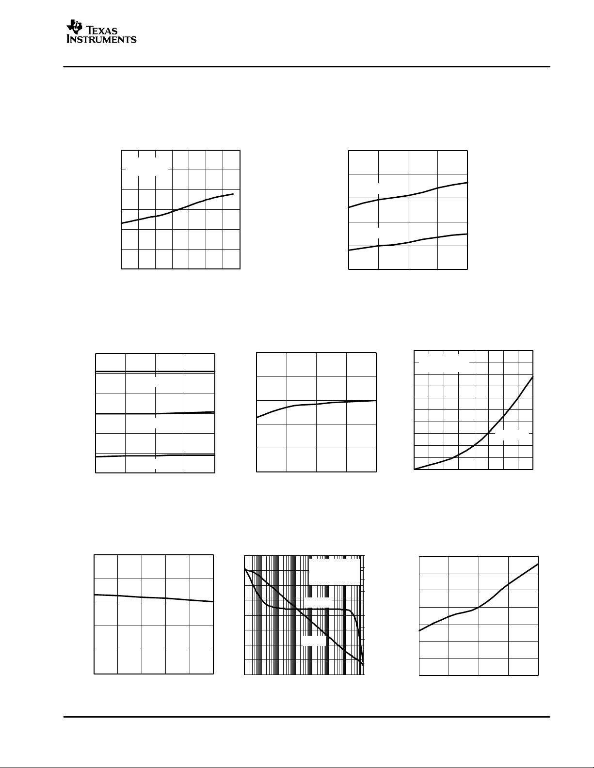
TYPICAL CHARACTERISTICS
DRAIN-SOURCE
ON-STATE RESISTANCE
vs
JUNCTION TEMPERATURE
60
Ω
VI = 5 V,
IO = 8 A
50
40
30
20
10
Drain Source On-State Reststance − m
0
−40 −15 10 35 60 85 110 135
TJ − Junction Temperature − °C
Figure 1
EXTERNALLY SET
OSCILLATOR FREQUENCY
vs
JUNCTION TEMPERATURE
800
700
600
500
400
300
f − Externally Set Oscillator Frequency − kHz
200
−40 0 25 85 125
RT = 68 k
RT = 100 k
RT = 180 k
TJ − Junction Temperature − °C
Figure 3
f − Internally Set Oscillator Frequency − kHz
VOLTAGE REFERENCE
vs
JUNCTION TEMPERATURE
0.895
0.893
0.891
0.889
− Voltage Reference − V
ref
0.887
V
0.885
−40 0 25 85 125
TJ − Junction Temperature − °C
Figure 4
INTERNALLY SET
OSCILLATOR FREQUENCY
vs
JUNCTION TEMPERATURE
750
650
SYNC ≥ 2.5 V
550
450
SYNC ≤ 0.8 V
350
250
−40 0 25 85 125
TJ − Junction Temperature − °C
Figure 2
DEVICE POWER LOSSES
5
4.5
4
3.5
3
2.5
2
1.5
Device Power Losses − W
1
0.5
0
012345678
LOAD CURRENT
TJ = 125°C
fs = 700 kHz
IL − Load Current − A
vs
VI = 5 V
Figure 5
OUTPUT VOLTAGE REGULATION
vs
INPUT VOLTAGE
4.5 4.8 5.1 5.4 5.7 6
V
− Input Voltage − V
I
− Output Voltage Regulation − V
V
0.895
0.893
0.891
0.889
0.887
O
0.885
Figure 6
ERROR AMPLIFIER
OPEN LOOP RESPONSE
140
120
100
80
60
Gain − dB
40
20
0
−20
1 100 1 k 1 M
10 10 k 100 k 10 M
f − Frequency − Hz
RL = 10 kΩ,
CL = 160 pF,
TA = 25°C
Phase
Gain
Figure 7
0
−20
−40
−60
−80
−100
−120
−140
−160
−180
−200
rees
Phase − De
INTERNAL SLOW-START TIME
vs
JUNCTION TEMPERATURE
3.80
3.65
3.50
3.35
3.20
3.05
Internal Slow-Start Time − ms
2.90
2.75
−40 0 25 85 125
TJ − Junction Temperature − °C
Figure 8
7
Page 8

TPS54810
SLVS420B − MARCH 2002 − R EVISED FEBRUARY 2005
APPLICATION INFORMATION
Figure 9 shows the schematic diagram for a typical
TPS54810 application. The TPS54810 (U1) can provide
up to 8 A of output current at a nominal output voltage of
V
I
C10
10 µF
C1
1000 pF
R1
10 kΩ
R2
301 Ω
C12
10 µF
R5
10 kΩ
R3
10 kΩ
150 pF
R4
9.76 kΩ
C2
R6
71.5 kΩ
C6
0.047 µF
C3
1 µF
C4
3300 pF
28
27
26
25
4
3
2
1
RT
SYNC
SS/ENA
VBIAS
PWRGD
COMP
VSENSE
AGND
U1
TPS54810PWP
PWRPAD
1.8 V. For proper thermal performance, the PowerPAD
underneath the integrated circuit TPS54810 needs to be
soldered well to the printed-circuit board.
24
VIN
23
VIN
22
VIN
21
VIN
20
VIN
14
PH
13
PH
12
PH
PH
PH
PH
PH
PH
PH
BOOT
PGND
PGND
PGND
PGND
PGND
11
10
9
8
7
6
5
19
18
17
16
15
C9
0.047 µF
0.65 µH
R7
2.4 Ω
C11
3300 pF
L1
C8
22 µF
C7
22 µFC522 µF
www.ti.com
V
O
Analog and Power Grounds are Tied at the Pad Under the Package of IC
Figure 9. Application Circuit
COMPONENT SELECTION
The values for the components used in this design
example were selected for low output ripple voltage and
small PCB area. Additional design information is available
at www.ti.com.
INPUT FILTER
The input voltage is a nominal 5 VDC. The input filter C10
is a 10-µF ceramic capacitor (Taiyo Yuden). C12, also a
10-µF ceramic capacitor (Taiyo Yuden) provides high
frequency decoupling of the TPS54810 from the input
supply and must be located as close as possible to the
device. Ripple current is carried in both C10 and C12, and
the return path to PGND should avoid the current
circulating in the output capacitors C5, C7, and C8.
FEEDBACK CIRCUIT
The values for these components have been selected to
provide low output ripple voltage. The resistor divider
network of R1 and R4 sets the output voltage for the circuit
at 1.8 V. R1, along with R2, R3, C1, C2, and C4 forms the
loop compensation network for the circuit. For this design,
a Type 3 topology is used.
OPERATING FREQUENCY
In the application circuit, RT is grounded through a 71.5 kΩ
resistor to select the operating frequency of 700 kHz. To
set a different frequency, place a 68 kΩ to 180 kΩ resistor
between RT (pin 28) and analog ground or leave RT
floating to select the default of 350 kHz. The resistance can
be approximated using the following equation:
R +
500 kHz
Switching Frequency
100 [kW]
(1)
OUTPUT FILTER
The output filter is composed of a 0.65-µH inductor and
3 x 22-µF capacitor. The inductor is a low dc resistance
(0.017 Ω) type, Pulse Engineering PA0277. The
capacitors used are 22-µF, 6.3 V ceramic types with X5R
dielectric. The feedback loop is compensated so that the
unity gain frequency is approximately 75 kHz.
8
Page 9

www.ti.com
TPS54810
SLVS420B − MARCH 2002 − R EVISED FEBRUARY 2005
PCB LAYOUT
Figure 10 shows a generalized PCB layout guide for the
TPS54810
The VIN pins are connected together on the printed-circuit
board (PCB) and bypassed with a low-ESR
ceramic-bypass capacitor. Care should be taken to
minimize the loop area formed by the bypass capacitor
connections, the VIN pins, and the TPS54810 ground
pins. The minimum recommended bypass capacitance is
10-µF ceramic capacitor with a X5R or X7R dielectric and
the optimum placement is closest to the VIN pins and the
PGND pins.
The TPS54810 has two internal grounds (analog and
power). Inside the TPS54810, the analog ground ties to all
of the noise sensitive signals, while the power ground ties
to the noisier power signals. Noise injected between the
two grounds can degrade the performance of the
TPS54810, particularly at higher output currents. Ground
noise on an analog ground plane can also cause problems
with some of the control and bias signals. For these
reasons, separate analog and power ground traces are
recommended. There is an area of ground on the top layer
directly under the IC, with an exposed area for connection
to the PowerPAD. Use vias to connect this ground area to
any internal ground planes. Additional vias are also used
at the ground side of the input and output filter capacitors.
The AGND and PGND pins are tied to the PCB ground by
connecting them to the ground area under the device as
shown. The only components that tie directly to the power
ground plane are the input capacitors, the output
capacitors, the input voltage decoupling capacitor, and the
PGND pins of the TPS54810. Use a separate wide trace
for the analog ground signal path. The analog ground is
used for the voltage set point divider, timing resistor RT,
slow-start capacitor and bias capacitor grounds. Connect
this trace directly to AGND (Pin 1).
The PH pins are tied together and routed to the output
inductor. Since the PH connection is the switching node,
the inductor is located close to the PH pins. The area of the
PCB conductor is minimized to prevent excessive
capacitive coupling.
Connect the boot capacitor between the phase node and
the BOOT pin as shown Keep the boot capacitor close to
the IC and minimize the conductor trace lengths.
Connect the output filter capacitor(s) as shown between
the VOUT trace and PGND. It is important to keep the loop
formed by the PH pins, L
OUT
, C
and PGND as small as
OUT
practical.
Place the compensation components from the VOUT trace
to the VSENSE and COMP pins. Do not place these
components too close to the PH trace. Due to the size of
the IC package and the device pin-out, they must be routed
close, but maintain as much separation as possible while
still keeping the layout compact.
Connect the bias capacitor from the VBIAS pin to analog
ground using the isolated analog ground trace. If a
slow-start capacitor or RT resistor is used, or if the SYNC
pin is used to select 350-kHz operating frequency, connect
them to this trace.
9
Page 10

TPS54810
SLVS420B − MARCH 2002 − R EVISED FEBRUARY 2005
COMPENSA TION
NETWORK
VOUT
BOOT
CAPACITOR
ANALOG GROUND TRACE
AGND
VSENSE
COMP
PWRGD
BOOT
PH
PH
EXPOSED
POWERP AD
SS/ENA
AREA
SYNC
VBIAS
VIN
VIN
VIN
www.ti.com
RT
FREQUENCY SET RESISTOR
SLOW ST ART
CAPACITOR
BIAS CAP ACITOR
OUTPUT INDUCTOR
OUTPUT
FILTER
CAPACITOR
PH
PH
PH
PH
PH
PH
PH
PH
TOPSIDE GROUND AREA
Figure 10. PCB Layout
VIN
VIN
PGND
PGND
PGND
PGND
PGND
VIA to Ground Plane
VIN
INPUT
BYPASS
CAPACITOR
INPUT
BULK
FILTER
10
Page 11

www.ti.com
TPS54810
SLVS420B − MARCH 2002 − R EVISED FEBRUARY 2005
LAYOUT CONSIDERATIONS FOR THERMAL
PERFORMANCE
For operation at full rated load current, the analog ground
plane must provide adequate heat dissipating area. A 3
inch by 3 inch plane of 1 ounce copper is recommended,
though not mandatory, depending on ambient temperature
and airflow. Most applications have larger areas of internal
ground plane available, and the PowerPAD should be
connected to the largest area available. Additional areas
on the top or bottom layers also help dissipate heat, and
Minimum Recommended Thermal Vias: 8 x 0.013 Diameter Inside
8 PL
Ø0.01804 PL
Connect Pin 1 to Analog Ground Plane
in This Area for Optimum Performance
0.0339
0.0650
0.0500
0.3478
0.3820
Minimum Recommended Top
Side Analog Ground Area
0.0500
0.0500
0.0650
0.0339
Ø0.0130
Powerpad Area 4 x 0.018 Diameter Under Device as Shown.
Additional 0.018 Diameter Vias May Be Used if Top Side Analog Ground
Area Is Extended.
any area available should be used when 8 A or greater
operation is desired. Connection from the exposes area of
the PowerPAD to the analog ground plane layer should be
made using 0.013 inch diameter vias to avoid solder
wicking through the vias. Eight vias should be in the
PowerPAD area with four additional vias located under the
device package. The size of the vias under the package,
but not in the exposed thermal pad area, can be increased
to 0.018. Additional vias beyond the twelve recommended
that enhance thermal performance should be included in
areas not under the device package.
0.0150
0.06
0.2090
0.0256
Minimum Recommended Exposed
0.1700
0.1340
0.0630
0.0400
Copper Area for Powerpad. 5-mil
Stencils May Require 10 Percent
Larger Area
Figure 11. Recommended Land Pattern for the 28−Pin PWP PowerPAD
11
Page 12

TPS54810
SLVS420B − MARCH 2002 − R EVISED FEBRUARY 2005
PERFORMANCE GRAPHS (FROM APPLICATION CIRCUIT SHOWN IN FIGURE 9)
www.ti.com
EFFICIENCY
vs
100
95
90
85
80
75
70
Efficiency − %
65
60
55
50
OUTPUT CURRENT
VI = 5 V
VO = 1.8 V
fs = 700 kHz
0246810
IO − Output Current − A
Figure 12
AMBIENT TEMPERATURE
125
OUTPUT CURRENT
115
C
°
105
95
85
75
65
55
− Ambient Temperature −
45
A
T
35
25
01234
vs
IO − Output Current − A
(1)
TJ = 25°C
fs = 700 kHz
VI = 5 V
567 8
Figure 15
LOAD REGULATION
vs
OUTPUT CURRENT
1.003
1.002
1.001
1
Load Regulation
0.999
0.998
0.997
0246810
IO − Output Current − A
VI = 5 V
VO = 1.8 V
TA = 25°C
fs = 700 kHz
Figure 13
OUTPUT RIPPLE VOLTAGE
VI = 5 V
VO = 1.8 V
IO = 6 A
fs = 700 kHz
Output Ripple Voltage − 10 mV/div
t − Time − 1 µs/div
Figure 16
LINE REGULATION
vs
INPUT VOLTAGE
1.001
1.0008
1.0006
1.0004
1.0002
0.9998
Line Regulation
0.9996
0.9994
0.9992
0.999
8 A
1
4 A
4.5 4.7 4.9 5.1 5.3 5.5 5.7 5.9
0 A
VI − Input Voltage − V
Figure 14
TRANSIENT RESPONSE
VI = 5 V
− Output Voltage − 100 mV/div
O
V
2 A to 6.5 A
t − Time − 20 µs/div
Figure 17
VI = 5 V
VO = 1.8 V
TA = 25°C
fs = 700 kHz
− Output Current − 2 A/div
O
I
SLOW-START TIMING
VI = 5 V,
0.04 µF
Slow-start Cap
Input Voltage − 2 V/div
4.0 ms/div
Figure 18
(1)
Safe operating area is applicable to the test board conditions in the Dissipation Ratings
12
Output Voltage − 2 V/div
Page 13

www.ti.com
TPS54810
SLVS420B − MARCH 2002 − R EVISED FEBRUARY 2005
DETAILED DESCRIPTION
Under Voltage Lock Out (UVLO)
The TPS54810 incorporates an under voltage lockout
circuit to keep the device disabled when the input voltage
(VIN) is insufficient. During power up, internal circuits are
held inactive until VIN exceeds the nominal UVLO
threshold voltage of 3.80 V. Once the UVLO start threshold
is reached, device start-up begins. The device operates
until VIN falls below the nominal UVLO stop threshold of
3.5 V. Hysteresis in the UVLO comparator, and a 2.5-µs
rising and falling edge deglitch circuit reduce the likelihood
of shutting the device down due to noise on VIN.
Slow-Start/Enable (SS/ENA)
The slow-start/enable pin provides two functions. First, the
pin acts as an enable (shutdown) control by keeping the
device turned off until the voltage exceeds the start
threshold voltage of approximately 1.2 V. When SS/ENA
exceeds the enable threshold, device start up begins. The
reference voltage fed to the error amplifier is linearly
ramped up from 0 V to 0.891 V in 3.35 ms. Similarly, the
converter output voltage reaches regulation in
approximately 3.35 ms. Voltage hysteresis and a 2.5-µs
falling edge deglitch circuit reduce the likelihood of
triggering the enable due to noise.
The second function of the SS/ENA pin provides an
external means of extending the slow-start time with a
low-value capacitor connected between SS/ENA and
AGND.
Adding a capacitor to the SS/ENA pin has two effects on
start-up. First, a delay occurs between release of the
SS/ENA pin and start up of the output. The delay is
proportional to the slow-start capacitor value and lasts until
the SS/ENA pin reaches the enable threshold. The
start-up delay is approximately:
td+ C
(SS)
Second, as the output becomes active, a brief ramp-up at
the internal slow-start rate may be observed before the
externally set slow-start rate takes control and the output
rises at a rate proportional to the slow-start capacitor. The
ramp-up time set by the capacitor is approximately:
t
+ C
(d)
(SS)
The actual ramp-up time is likely to be less than the above
approximation due to the brief ramp-up at the internal rate.
VBIAS Regulator (VBIAS)
The VBIAS regulator provides internal analog and digital
blocks with a stable supply voltage over variations in
junction temperature and input voltage. A high quality,
1.2 V
5 mA
0.7 V
5 mA
(2)
(3)
low-ESR, ceramic bypass capacitor is required on the
VBIAS pin. X7R or X5R grade dielectrics are
recommended because their values are more stable over
temperature. The bypass capacitor should be placed close
to the VBIAS pin and returned to AGND.
External loading on VBIAS is allowed, with the caution that
internal circuits require a minimum VBIAS of 2.70 V, and
external loads on VBIAS with ac or digital switching noise
may degrade performance. The VBIAS pin may be useful
as a reference voltage for external circuits.
Voltage Reference
The voltage reference system produces a precise V
ref
signal by scaling the output of a temperature stable
bandgap circuit. During manufacture, the bandgap and
scaling circuits are trimmed to produce 0.891 V at the
output of the error amplifier, with the amplifier connected
as a voltage follower. The trim procedure adds to the high
precision regulation of the TPS54810, since it cancels
offset errors in the scale and error amplifier circuits.
Oscillator and PWM Ramp
The oscillator frequency can be set to internally fixed
values of 350 kHz or 550 kHz using the SYNC pin as a
static digital input. If a different frequency of operation is
required for the application, the oscillator frequency can be
externally adjusted from 280 to 700 kHz by connecting a
resistor between the RT pin and AGND and floating the
SYNC pin. The switching frequency is approximated by
the following equation, where R is the resistance from RT
to AGND:
Switching Frequency +
100 kW
R
500 [kHz]
(4)
External synchronization of the PWM ramp is possible
over the frequency range of 330 kHz to 700 kHz by driving
a synchronization signal into SYNC and connecting a
resistor from RT to AGND. Choose an RT resistor which
sets the free running frequency to 80% of the
synchronization signal. The following table summarizes
the frequency selection configurations:
SWITCHING FRE-
QUENCY
350 kHz, internally set Float or AGND Float
550 kHz, internally set =2.5 V Float
Externally set 280 kHz
to 700 kHz
Externally synchronized frequency
SYNC PIN RT PIN
Float R = 68 k to 180 k
Synchronization
signal
R = RT value for 85%
of external synchronization frequency
Error Amplifier
The high performance, wide bandwidth, voltage error
amplifier sets the TPS54810 apart from most dc/dc
converters. The user is given the flexibility to use a wide
range of output L and C filter components to suit the
13
Page 14

TPS54810
SLVS420B − MARCH 2002 − R EVISED FEBRUARY 2005
www.ti.com
particular application needs. Type 2 or type 3 compensation can be employed using external compensation
components.
PWM Control
Signals from the error amplifier output, oscillator, and
current limit circuit are processed by the PWM control
logic. Referring to the internal block diagram, the control
logic includes the PWM comparator, OR gate, PWM latch,
and portions of the adaptive dead-time and control logic
block. During steady-state operation below the current
limit threshold, the PWM comparator output and oscillator
pulse train alternately reset and set the PWM latch. Once
the PWM latch is reset, the low-side FET remains on for a
minimum duration set by the oscillator pulse width. During
this period, the PWM ramp discharges rapidly to its valley
voltage. When the ramp begins to charge back up, the
low-side FET turns off and high-side FET turns on. As the
PWM ramp voltage exceeds the error amplifier output
voltage, the PWM comparator resets the latch, thus
turning off the high-side FET and turning on the low-side
FET. The low-side FET remains on until the next oscillator
pulse discharges the PWM ramp.
During transient conditions, the error amplifier output
could be below the PWM ramp valley voltage or above the
PWM peak voltage. If the error amplifier is high, the PWM
latch is never reset and the high-side FET remains on until
the oscillator pulse signals the control logic to turn the
high-side FET off and the low-side FET on. The device
operates at its maximum duty cycle until the output voltage
rises to the regulation set-point, setting VSENSE to
approximately the same voltage as VREF. If the error
amplifier output is low, the PWM latch is continually reset
and the high-side FET does not turn on. The low-side FET
remains on until the VSENSE voltage decreases to a
range that allows the PWM comparator to change states.
The TPS54810 is capable of sinking current continuously
until the output reaches the regulation set-point.
If the current limit comparator trips for longer than 100 ns,
the PWM latch resets before the PWM ramp exceeds the
error amplifier output. The high-side FET turns off and
low-side FET turns on to decrease the energy in the output
inductor and consequently the output current. This
process is repeated each cycle in which the current limit
comparator is tripped.
Dead-Time Control and MOSFET Drivers
Adaptive dead-time control prevents shoot-through
current from flowing in both N-channel power MOSFETs
during the switching transitions by actively controlling the
turnon times of the MOSFET drivers. The high-side driver
does not turn on until the voltage at the gate of the low-side
FET is below 2 V. While the low-side driver does not turn
on until the voltage at the gate of the high-side MOSFET
is below 2 V.
The high-side and low-side drivers are designed with
300-mA source and sink capability to quickly drive the
power MOSFETs gates. The low-side driver is supplied
from VIN, while the high-side drive is supplied from the
BOOT pin. A bootstrap circuit uses an external BOOT
capacitor and an internal 2.5-Ω bootstrap switch
connected between the VIN and BOOT pins. The
integrated bootstrap switch improves drive efficiency and
reduces external component count.
Overcurrent Protection
The cycle by cycle current limiting is achieved by sensing
the current flowing through the high-side MOSFET and
comparing this signal to a preset overcurrent threshold.
The high side MOSFET is turned off within 200 ns of
reaching the current limit threshold. A 100 ns leading edge
blanking circuit prevents false tripping of the current limit
when the high side switch is turning on. Current limit
detection occurs only when current flows from VIN to PH
when sourcing current to the output filter. Load protection
during current sink operation is provided by thermal
shutdown.
Thermal Shutdown
The device uses the thermal shutdown to turn off the power
MOSFETs and disable the controller if the junction
temperature exceeds 150°C. The device is released from
shutdown automatically when the junction temperature
decreases to 10°C below the thermal shutdown trip point,
and starts up under control of the slow-start circuit.
Thermal shutdown provides protection when an overload
condition is sustained for several milliseconds. With a
persistent fault condition, the device cycles continuously;
starting up by control of the soft-start circuit, heating up due
to the fault condition, and then shutting down upon
reaching the thermal shutdown trip point. This sequence
repeats until the fault condition is removed.
Power Good (PWRGD)
The power good circuit monitors for under voltage
conditions on VSENSE. If the voltage on VSENSE is 10%
below the reference voltage, the open-drain PWRGD
output is pulled low. PWRGD is also pulled low if VIN is
less than the UVLO threshold or SS/ENA is low. When
VIN ≥ UVLO threshold, SS/ENA ≥ enable threshold, and
VSENSE > 90% of V
, the open drain output of the
ref
PWRGD pin is high. A hysteresis voltage equal to 3% of
V
and a 35 µs falling edge deglitch circuit prevent
ref
tripping of the power good comparator due to high
frequency noise.
14
Page 15

PACKAGE OPTION ADDENDUM
www.ti.com
5-Feb-2007
PACKAGING INFORMATION
Orderable Device Status
(1)
Package
Type
Package
Drawing
Pins Package
Qty
Eco Plan
TPS54810PWP ACTIVE HTSSOP PWP 28 50 Green (RoHS &
no Sb/Br)
TPS54810PWPG4 ACTIVE HTSSOP PWP 28 50 Green (RoHS &
no Sb/Br)
TPS54810PWPR ACTIVE HTSSOP PWP 28 2000 Green (RoHS &
no Sb/Br)
TPS54810PWPRG4 ACTIVE HTSSOP PWP 28 2000 Green(RoHS &
no Sb/Br)
(1)
The marketing status values are defined as follows:
ACTIVE: Product device recommended for new designs.
LIFEBUY: TI has announced that the device will be discontinued, and a lifetime-buy period is in effect.
NRND: Not recommended for new designs. Device is in production to support existing customers, but TI does not recommend using this part in
a new design.
PREVIEW: Device has been announced but is not in production. Samples may or may not be available.
OBSOLETE: TI has discontinued the production of the device.
(2)
Eco Plan - The planned eco-friendly classification: Pb-Free (RoHS), Pb-Free (RoHS Exempt), or Green (RoHS & no Sb/Br) - please check
http://www.ti.com/productcontent for the latest availability information and additional product content details.
TBD: The Pb-Free/Green conversion plan has not been defined.
Pb-Free (RoHS): TI's terms "Lead-Free" or "Pb-Free" mean semiconductor products that are compatible with the current RoHS requirements
for all 6 substances, including the requirement that lead not exceed 0.1% by weight in homogeneous materials. Where designed to be soldered
at high temperatures, TI Pb-Free products are suitable for use in specified lead-free processes.
Pb-Free (RoHS Exempt): This component has a RoHS exemption for either 1) lead-based flip-chip solder bumps used between the die and
package, or 2) lead-based die adhesive used between the die and leadframe. The component is otherwise considered Pb-Free (RoHS
compatible) as defined above.
Green (RoHS & no Sb/Br): TI defines "Green" to mean Pb-Free (RoHS compatible), and free of Bromine (Br) and Antimony (Sb) based flame
retardants (Br or Sb do not exceed 0.1% by weight in homogeneous material)
(2)
Lead/Ball Finish MSL Peak Temp
CU NIPDAU Level-2-260C-1 YEAR
CU NIPDAU Level-2-260C-1 YEAR
CU NIPDAU Level-2-260C-1 YEAR
CU NIPDAU Level-2-260C-1 YEAR
(3)
(3)
MSL, Peak Temp. -- The Moisture Sensitivity Level rating according to the JEDEC industry standard classifications, and peak solder
temperature.
Important Information and Disclaimer:The information provided on this page represents TI's knowledge and belief as of the date that it is
provided. TI bases its knowledge and belief on information provided by third parties, and makes no representation or warranty as to the
accuracy of such information. Efforts are underway to better integrate information from third parties. TI has taken and continues to take
reasonable steps to provide representative and accurate information but may not have conducted destructive testing or chemical analysis on
incoming materials and chemicals. TI and TI suppliers consider certain information to be proprietary, and thus CAS numbers and other limited
information may not be available for release.
In no event shall TI's liability arising out of such information exceed the total purchase price of the TI part(s) at issue in this document sold by TI
to Customer on an annual basis.
Addendum-Page 1
Page 16

PACKAGE MATERIALS INFORMATION
www.ti.com
TAPE AND REEL INFORMATION
11-Mar-2008
*All dimensions are nominal
Device Package
Type
TPS54810PWPR HTSSOP PWP 28 2000 330.0 16.4 6.9 10.2 1.8 12.0 16.0 Q1
Package
Drawing
Pins SPQ Reel
Diameter
(mm)
Reel
Width
W1 (mm)
A0 (mm) B0 (mm) K0 (mm) P1
(mm)W(mm)
Pin1
Quadrant
Pack Materials-Page 1
Page 17

PACKAGE MATERIALS INFORMATION
www.ti.com
11-Mar-2008
*All dimensions are nominal
Device Package Type Package Drawing Pins SPQ Length (mm) Width (mm) Height (mm)
TPS54810PWPR HTSSOP PWP 28 2000 346.0 346.0 33.0
Pack Materials-Page 2
Page 18

Page 19

Page 20

Page 21

IMPORTANT NOTICE
Texas Instruments Incorporated and its subsidiaries (TI) reserve the right to make corrections, modifications, enhancements, improvements,
and other changes to its products and services at any time and to discontinue any product or service without notice. Customers should
obtain the latest relevant information before placing orders and should verify that such information is current and complete. All products are
sold subject to TI’s terms and conditions of sale supplied at the time of order acknowledgment.
TI warrants performance of its hardware products to the specifications applicable at the time of sale in accordance with TI’s standard
warranty. Testing and other quality control techniques are used to the extent TI deems necessary to support this warranty. Except where
mandated by government requirements, testing of all parameters of each product is not necessarily performed.
TI assumes no liability for applications assistance or customer product design. Customers are responsible for their products and
applications using TI components. To minimize the risks associated with customer products and applications, customers should provide
adequate design and operating safeguards.
TI does not warrant or represent that any license, either express or implied, is granted under any TI patent right, copyright, mask work right,
or other TI intellectual property right relating to any combination, machine, or process in which TI products or services are used. Information
published by TI regarding third-party products or services does not constitute a license from TI to use such products or services or a
warranty or endorsement thereof. Use of such information may require a license from a third party under the patents or other intellectual
property of the third party, or a license from TI under the patents or other intellectual property of TI.
Reproduction of TI information in TI data books or data sheets is permissible only if reproduction is without alteration and is accompanied
by all associated warranties, conditions, limitations, and notices. Reproduction of this information with alteration is an unfair and deceptive
business practice. TI is not responsible or liable for such altered documentation. Information of third parties may be subject to additional
restrictions.
Resale of TI products or services with statements different from or beyond the parameters stated by TI for that product or service voids all
express and any implied warranties for the associated TI product or service and is an unfair and deceptive business practice. TI is not
responsible or liable for any such statements.
TI products are not authorized for use in safety-critical applications (such as life support) where a failure of the TI product would reasonably
be expected to cause severe personal injury or death, unless officers of the parties have executed an agreement specifically governing
such use. Buyers represent that they have all necessary expertise in the safety and regulatory ramifications of their applications, and
acknowledge and agree that they are solely responsible for all legal, regulatory and safety-related requirements concerning their products
and any use of TI products in such safety-critical applications, notwithstanding any applications-related information or support that may be
provided by TI. Further, Buyers must fully indemnify TI and its representatives against any damages arising out of the use of TI products in
such safety-critical applications.
TI products are neither designed nor intended for use in military/aerospace applications or environments unless the TI products are
specifically designated by TI as military-grade or "enhanced plastic." Only products designated by TI as military-grade meet military
specifications. Buyers acknowledge and agree that any such use of TI products which TI has not designated as military-grade is solely at
the Buyer's risk, and that they are solely responsible for compliance with all legal and regulatory requirements in connection with such use.
TI products are neither designed nor intended for use in automotive applications or environments unless the specific TI products are
designated by TI as compliant with ISO/TS 16949 requirements. Buyers acknowledge and agree that, if they use any non-designated
products in automotive applications, TI will not be responsible for any failure to meet such requirements.
Following are URLs where you can obtain information on other Texas Instruments products and application solutions:
Products Applications
Amplifiers amplifier.ti.com Audio www.ti.com/audio
Data Converters dataconverter.ti.com Automotive www.ti.com/automotive
DSP dsp.ti.com Broadband www.ti.com/broadband
Clocks and Timers www.ti.com/clocks Digital Control www.ti.com/digitalcontrol
Interface interface.ti.com Medical www.ti.com/medical
Logic logic.ti.com Military www.ti.com/military
Power Mgmt power.ti.com Optical Networking www.ti.com/opticalnetwork
Microcontrollers microcontroller.ti.com Security www.ti.com/security
RFID www.ti-rfid.com Telephony www.ti.com/telephony
RF/IF and ZigBee® Solutions www.ti.com/lprf Video & Imaging www.ti.com/video
Mailing Address: Texas Instruments, Post Office Box 655303, Dallas, Texas 75265
Copyright © 2008, Texas Instruments Incorporated
Wireless www.ti.com/wireless
 Loading...