

Page 1

Using the TPS54386EVM
User's Guide
March 2008 Power Supply MAN
SLUU286
Page 2

Using the TPS54386EVM
User's Guide
Literature Number: SLUU286
March 2008
Page 3

User's Guide
SLUU286 – March 2008
A 12-V Input, 5.0-V and 3.3-V Output, 2-A
Non-Synchronous Buck Converter
1 Introduction
The TPS54386EVM evaluation module (EVM) is a dual non-synchronous buck converter providing fixed
5.0-V and 3.3-V output at up to 2 A each from a 12-V input bus. The EVM is designed to start up from a
single supply, so no additional bias voltage is required for start-up. The module uses the TPS54386 Dual
Non-Synchronous Buck Converter with Integral High-Side FET.
1.1 Description
TPS54386EVM is designed to use a regulated 12-V (+10% / -20%) bus to produce two regulated power
rails, 5.0 V and 3.3 V at up to 2 A of load current each. TPS54386EVM is designed to demonstrate the
TPS54386 in a typical 12-V bus system while providing a number of test points to evaluate the
performance of the TPS54386 in a given application. The EVM can be modified to other input or output
voltages by changing some of the components.
1.2 Applications
• Non-Isolated Low Current Point of Load and Voltage Bus Converters
• Consumer Electronics
• LCD TV
• Computer Peripherals
• Digital Set Top Box
1.3 Features
• 12-V (+10% / -20%) Input Range
• 5.0-V and 3.3-V Fixed Output Voltage, Adjustable with Resistor Change
• 2-A
• 600-kHz Switching Frequency (fixed by TPS54386)
• Internal Switching MOSFET and External Rectifier Diode
• Double Sided 2 Active Layer PCB (all components on top side, test point signals routed on internal
• Active Converter Area Less than 1.8 Square Inches (0.89” x 1.97”)
• Convenient Test Points (used for probing switching waveforms and non-invasive loop response testing)
Steady State Output Current (3 A Peak)
DC
layers)
SLUU286 – March 2008 A 12-V Input, 5.0-V and 3.3-V Output, 2-A Non-Synchronous Buck Converter 3
Submit Documentation Feedback
Page 4

www.ti.com
TPS54386EVM Electrical Performance Specifications
2 TPS54386EVM Electrical Performance Specifications
SYMBOL PARAMETER MIN TYP MAX UNITS
Input Characterstics
V
IN
I
IN
V
IN_UVLO
Output Characterstics
V
OUT1
V
OUT2
V
OUT_ripple
I
OUT1
I
OUT2
I
OCP1
I
OCP2
Systems Characterstics
F
SW
η pk Peak efficiency VIN= nom - 90% η Full load efficiency VIN= nom, I
Top VIN= min to max, I
Input coltage 9.6 12 13.2 V
Input current VIN= nom, I
No load input current VIN= nom, I
Input UVLO I
Output voltage 1 VIN= nom, I
Output voltage 2 VIN= nom, I
Line regulation VIN= min to max - - 1%
Load regulation IOUT = min to max - - 1%
Output voltage ripple VIN= nom, I
Output current 1 VIN= min to max 0 2.0
Output current 2 VIN= min to max 0 2.0
Output over current
Channel 1
Output over current
Channel 2
Switching frequency 510 630 750 kHz
Operating temperature ° C
range
Table 1. Electrical Performance Specifications
OUT
OUT
= min to max 4.0 4.2 4.4 V
OUT
OUT
OUT
OUT
VIN= nom, V
VIN= nom, V
OUT
OUT
OUT
= max - 1.6 2.0 A
= 0 A - 12 20 mA
= nom 4.85 5.0 5.15
= nom 3.20 3.3 3.40
= max - - 30 mV
= V
= V
- 5% 3.1 3.7 4.5
OUT1
- 5% 3.1 3.7 4.5
OUT2
= max - 85% -
= min to max 0 25 60
OUT
V
pp
A
4 A 12-V Input, 5.0-V and 3.3-V Output, 2-A Non-Synchronous Buck Converter SLUU286 – March 2008
Submit Documentation Feedback
Page 5
www.ti.com
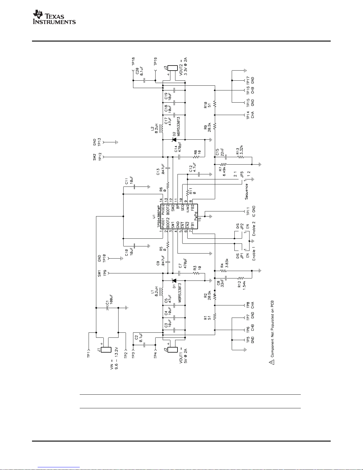
+
Schematic
3 Schematic
SLUU286 – March 2008 A 12-V Input, 5.0-V and 3.3-V Output, 2-A Non-Synchronous Buck Converter 5
Submit Documentation Feedback
Note: For reference only, see Table 3 , List of Materials for specific values.
Figure 1. TPS54386EVM Schematic
Page 6

www.ti.com
Schematic
3.1 Sequencing Jump (JP3)
The TPS54386EVM provides a 3-pin, 100-mil header and shunt for programming the TPS54386’s
sequencing function. Placing the JP3 shunt in the left position connects the sequence pin to BP and sets
the TPS54386 controller to sequence Channel 2 prior to Channel 1 when Enable 2 is activated. Placing
the JP3 shunt in the right position connects the sequence pin to GND and sets the TPS54386 converter to
sequence Channel 1 prior to Channel 1 when Enable 1 is activated. Removing the JP3 shunt disables
sequencing and allows Channel 1 and Channel 2 to be enabled independently.
3.2 Enable Jumpers (JP1 and JP2)
TPS54386EVM provides separate 3-pin, 100-mil headers and shunts for exercising the TPS54386 Enable
functions. When JP3 is removed placing the JP1 shunt in the left position connects EN1 to ground and
turns on Output 1 and placing the JP2 shunt in the left position connects EN2 to ground and turns on
Output 2.
When the JP3 shunt is in the LEFT position, placing the JP2 shunt in the left position connects EN2 to
ground and turns on first Output 2 and then Output 1.
When the JP3 shunt is in the RIGHT position, placing the JP1 shunt in the left position connects EN1 to
ground and turns on first Output 1 and then Output 2.
3.3 Test Point Descriptions
TEST POINT LABLE USE SECTION
TP1 VIN Monitor input voltage Section 3.3.1
TP2 GND Ground for input voltage Section 3.3.1
TP3 VOUT1 Monitor VOUT1 Voltage Section 3.3.2
TP4 GND Ground for VOUT1 voltage Section 3.3.2
TP5 GND Ground for Channel B loop monitoring Section 3.3.3
TP6 CHB Channel B for loop monitoring Section 3.3.3
TP7 GND Ground for Channel A loop monitoring Section 3.3.3
TP8 CHA Channel A for loop monitoring Section 3.3.3
TP9 SW1 Monitor switching node of Channel 1 Section 3.3.4
TP10 GND Ground for switch node of Channel 1 Section 3.3.4
TP11 IC_GND Monitor device ground Section 3.3.5
TP12 SW2 Monitor switching node of Channel 2 Section 3.3.6
TP13 GND Ground for switch node of Channel 2 Section 3.3.6
TP14 CHA Channel A for loop monitoring Section 3.3.7
TP15 GND Ground for Channel A loop monitoring Section 3.3.7
TP16 CHB Channel B for loop monitoring Section 3.3.7
TP17 GND Ground for Channel B loop monitoring Section 3.3.7
TP18 VOUT2 Monitor VOUT2 voltage Section 3.3.8
TP19 GND Ground for VOUT2 voltage Section 3.3.8
Table 2. Test Point Descriptions
6 A 12-V Input, 5.0-V and 3.3-V Output, 2-A Non-Synchronous Buck Converter SLUU286 – March 2008
Submit Documentation Feedback
Page 7

www.ti.com
3.3.1 Input Voltage Monitoring (TP1 and TP2)
TPS54386EVM provides two test points for measuring the voltage applied to the module. This allows the
user to measure the actual module voltage without losses from input cables and connectors. All input
voltage measurements should be made between TP1 and TP2. To use TP1 and TP2, connect a voltmeter
positive terminal to TP1 and negative terminal to TP2.
3.3.2 Channel 1 Output Voltage Monitoring (TP3 and TP4)
TPS54386EVM provides two test points for measuring the voltage generated by the module. This allows
the user to measure the actual module output voltage without losses from output cables and connectors.
All output voltage measurements should be made between TP3 and TP4. To use TP3 and TP4, connect a
voltmeter positive terminal to TP3 and negative terminal to TP4. For Output ripple measurements, TP3
and TP4 allow a user to limit the ground loop area by using the Tip and Barrel measurement technique
shown in Figure 3 . All output ripple measurements should be made using the Tip and Barrel
measurement.
3.3.3 Channel 1 Loop Analysis (TP5, TP6, TP7 and TP8)
TPS54386EVM contains a 51- Ω series resistor (R1) in the feedback loop to allow for matched impedance
signal injection into the feedback for loop response analysis. An isolation transformer should be used to
apply a small (30 mV or less) signal across R1 through TP6 and TP8. By monitoring the ac injection level
at TP8 and the returned ac level at TP6, the power supply loop response can be determined.
3.3.4 Channel 1 Switching Waveforms (TP9 and TP10)
TPS54386EVM provides a test point and a local ground connection (TP10) for the monitoring of the
Channel 1 power stage switching waveform. Connect an oscilloscope probe to TP9 to monitor the switch
node voltage for Channel 1.
Schematic
3.3.5 TPS54386 Device Ground (TP11)
TPS54386EVM provides a test point for the device ground. To measure the device pin voltages, connect
the ground of the oscilloscope probe to TP11.
3.3.6 Channel 2 Switching Waveforms (TP12 and TP13)
TPS54386EVM provides a test point and a local ground connection (TP13) for the monitoring of the
Channel 1 power stage switching waveform. Connect an oscilloscope probe to TP12 to monitor the switch
node voltage for Channel 1.
3.3.7 Channel 2 Loop Analysis (TP14, TP15, TP16 and TP17)
TPS54386EVM contains a 51- Ω series resistor (R10) in the feedback loop to allow for matched
impedance signal injection into the feedback for loop response analysis. An isolation transformer should
be used to apply a small (30 mV or less) signal across R10 through TP14 and TP16. By monitoring the ac
injection level at TP14 and the returned ac level at TP16, the power supply loop response can be
determined.
3.3.8 Output Voltage Monitoring (TP18 and TP19)
TPS54386EVM provides two test points for measuring the voltage generated by the module. This allows
the user to measure the actual module output voltage without losses from output cables and connector
losses. All output voltage measurements should be made between TP18 and TP19. To use TP18 and
TP19, connect a voltmeter positive terminal to TP18 and negative terminal to TP19. For output ripple
measurements, TP18 and TP19 allow a user to limit the ground loop area by using the Tip and Barrel
measurement technique shown in Figure 3 . All output ripple measurements should be made using the Tip
and Barrel measurement.
SLUU286 – March 2008 A 12-V Input, 5.0-V and 3.3-V Output, 2-A Non-Synchronous Buck Converter 7
Submit Documentation Feedback
Page 8

www.ti.com
4 Test Set Up
4 4 Test Set Up
4.1 Equipment
4.1.1 Voltage Source
VIN: The input voltage source (VIN) should be a 0-15 V variable dc source capable of 5 A
to J1 as shown in Figure 3 .
4.1.2 Meters
• A1: 0-3 A
• V1: VIN, 0-15 V voltmeter
• V2: VOUT1 0-6 V voltmeter
• V3: VOUT2 0-4 V voltmeter
4.1.3 Loads
LOAD1: The Output1 Load (LOAD1) should be an electronic constant current mode load capable of 0-2
A
at 5.0 V
DC
LOAD2: The Output2 Load (LOAD2) should be an electronic constant current mode load capable of 0-2
A
at 3.3 V
DC
. Connect VIN
DC
, ammeter
DC
4.1.4 Oscilloscope
Oscilloscope: A digital or analog oscilloscope can be used to measure the ripple voltage on VOUT. The
oscilloscope should be set for 1-M Ω impedance, 20-MHz bandwidth, ac coupling, 1- µ s/division horizontal
resolution, 10-mV/division vertical resolution for taking output ripple measurements. TP3 and TP4 or TP18
and TP19 can be used to measure the output ripple voltages by placing the oscilloscope probe tip through
TP3 or TP18 and holding the ground barrel to TP4 or TP19 as shown in Figure 3 . For a hands free
approach, the loop in TP4 or TP19 can be cut and opened to cradle the probe barrel. Using a leaded
ground connection may induce additional noise due to the large ground loop area.
4.1.5 Recommended Wire Gauge
VIN to J1: The connection between the source voltage, VIN and J1 of HPA241 can carry as much as 5
A
. The minimum recommended wire size is AWG #16 with the total length of wire less than 4 feet (2
DC
feet input, 2 feet return).
J2 to LOAD1: The power connection between J2 of HPA241 and LOAD1 can carry as much as 2 A
The minimum recommended wire size is AWG #18, with the total length of wire less than 2 feet (1 foot
output, 1 foot return).
J3 to LOAD2: The power connection between J3 of HPA241 and LOAD2 can carry as much as 2 A
The minimum recommended wire size is AWG #18, with the total length of wire less than 2 feet (1 foot
output, 1 foot return).
4.1.6 Other
Fan: This evaluation module includes components that can get hot to the touch, because this EVM is not
enclosed to allow probing of circuit nodes, a small fan capable of 200-400 lfm is recommended to reduce
component surface temperatures to prevent user injury. The EVM should not be left unattended while
powered. The EVM should not be probed while the fan is not running.
.
DC
.
DC
A 12-V Input, 5.0-V and 3.3-V Output, 2-A Non-Synchronous Buck Converter8 SLUU286 – March 2008
Submit Documentation Feedback
Page 9

www.ti.com
4.2 Equipment Setup
FAN
LOAD1
5.0V @
2A
-
+
V2
-
+
See Tip and Barrel
Measurement for Vout
ripple
Oscilloscope
1MW, AC
20mV / div
20MHz
LOAD2
3.3V @
2A
+
-
V3
-
+
V1
+
-
A1
-
+
V
VIN
Shown in Figure 2 is the basic test set up recommended to evaluate the TPS54386EVM. Please note that
although the return for J1, J2 and JP3 are the same system ground, the connections should remain
separate as shown in Figure 2
4.2.1 Procedure
1. Working at an ESD workstation, make sure that any wrist straps, bootstraps or mats are connected
referencing the user to earth ground before power is applied to the EVM. Electrostatic smock and
safety glasses should also be worn.
2. Prior to connecting the dc input source, VIN, it is advisable to limit the source current from VIN to 5.0 A
maximum. Make sure VIN is initially set to 0 V and connected as shown in Figure 2 .
3. Connect the ammeter A1 (0-5 A range) between VIN and J1 as shown in Figure 2 .
4. Connect voltmeter V1 to TP1 and TP2 as shown in Figure 2 .
5. Connect LOAD1 to J2 as shown in Figure 2 . Set LOAD1 to constant current mode to sink 0 A
VIN is applied.
6. Connect voltmeter, V2 across TP3 and TP4 as shown in Figure 2 .
7. Connect LOAD2 to J3 as shown in Figure 2 . Set LOAD2 to constant current mode to sink 0 A
VIN is applied.
8. Connect voltmeter, V3 across TP18 and TP19 as shown in Figure 2 .
9. Place fan as shown in Figure 2 and turn on, making sure air is flowing across the EVM.
4.2.2 Diagram
4 Test Set Up
DC
DC
before
before
SLUU286 – March 2008 A 12-V Input, 5.0-V and 3.3-V Output, 2-A Non-Synchronous Buck Converter 9
Submit Documentation Feedback
Figure 2. TPS54386EVM Recommended Test Set-Up
Page 10

www.ti.com
TP4 /
TP19
TP3 /
TP18
Metal Ground Barrel
Probe Tip
Tip and Barrel Vout ripple measurement
FAN
V1
+
-
A1
-
+
V
VIN
LOAD1
5.0V @
2A
-
+
V2
-
+
LOAD2
3.3V @
2A
+
-
V3
-
+
Isolation
Transformer
4 Test Set Up
Figure 3. Tip and Barrel Measurement Technique (output ripple measurement using TP3 and TP4 or TP18
and TP19)
Figure 4. Control Loop Measurement Setup
A 12-V Input, 5.0-V and 3.3-V Output, 2-A Non-Synchronous Buck Converter10 SLUU286 – March 2008
Submit Documentation Feedback
Page 11

www.ti.com
4.3 Start Up / Shut Down Procedure
20
ChannelB
LOG
ChannelA
æ ö
´
ç ÷
è ø
1. Increase VIN from 0 V to 12 V
2. Vary LOAD1 from 0 – 2 A
3. Vary LOAD2 from 0 – 2 A
4. Vary VIN from 9.6 V
5. Decrease VIN to 0 V
DC
DC
to 13.2 V
6. Decrease LOAD1 to 0 A.
.
DC
DC
DC
DC
4.4 Output Ripple Voltage Measurement Procedure
1. Increase VIN from 0 V to 12 V
2. Adjust LOAD1 to desired load between 0 A
3. Adjust VIN to desired load between 9.6 V
4. Connect oscilloscope probe to TP3 and TP4 or TP18 and TP19 as shown in Figure 3 .
5. Measure output ripple.
6. Decrease VIN to 0 V
.
DC
7. Decrease LOAD1 to 0 A.
.
DC
4.5 Control Loop Gain and Phase Measurement Procedure
1. Connect 1 kHz to 1 MHz isolation transformer to TP6 and TP8 as show in Figure 4 .
2. Connect input signal amplitude measurement probe (Channel A) to TP8 as shown in Figure 4 .
3. Connect output signal amplitude measurement probe (Channel B) to TP6 as shown in Figure 4 .
4. Connect ground lead of Channel A and Channel B to TP5 & TP7 as shown in Figure 4 .
5. Inject 30 mV or less signal across R1 through isolation transformer.
6. Sweep frequency from 1 kHz to 1 MHz with 10 Hz or lower post filter.
DC
and 13.2 V
DC
and 2 A
4 Test Set Up
.
DC
.
DC
4.6 Equipment Shutdown
7. Control loop gain can be measured by:
8. Control loop phase is measured by the phase difference between Channel A and Channel B.
9. Control loop for Channel 2 can be measured by making the following substitutions.
a. Change TP6 to TP16
b. Change TP8 to TP14
c. Change TP5 to TP17
d. Change TP7 to TP15
10. Disconnect isolation transformer before making any other measurements (signal injection into
feedback may interfere with accuracy of other measurements).
1. Shut down oscilloscope
2. Shut down VIN
3. Shut down LOAD1
4. Shut down fan
SLUU286 – March 2008 A 12-V Input, 5.0-V and 3.3-V Output, 2-A Non-Synchronous Buck Converter 11
Submit Documentation Feedback
Page 12

www.ti.com
0.10 1.24
I
LOAD
- Load Curre nt - A
95
85
80
75
60
0.48 0.86 1.62
90
h - Efficiency - %
EFFICIENCY(V
OUT
= 5.0 V)
vs
LOADCURRENT
70
65
I
LOAD
- Load Curre nt - A
90
75
65
60
85
h - Efficiency - %
EFFICIENCY(V
OUT
= 3.3 V)
vs
LOADCURRENT
50
2.00
13.2 V
9.6 V
12.0 V
0.10 1.240.48 0.86 1.62 2.00
13.2 V
9.6 V
12.0 V
55
70
80
TPS54386EVM Typical Performance Data and Characteristic Curves
5 TPS54386EVM Typical Performance Data and Characteristic Curves
Figure 5 through Figure 9 present typical performance curves for the TPS54386EVM. Since actual
performance data can be affected by measurement techniques and environmental variables, these curves
are presented for reference and may differ from actual field measurements.
5.1 Efficiency
Figure 5. TPS54386EVM Efficiency verse Load Current V
3.3 V I
OUT2
=9.6-13.2 V, V
IN
= 0-2 A
OUT1
= 5.0 V I
OUT1
= 0-2 A, V
=
OUT2
A 12-V Input, 5.0-V and 3.3-V Output, 2-A Non-Synchronous Buck Converter12 SLUU286 – March 2008
Submit Documentation Feedback
Page 13

www.ti.com
5.2 Line and Load Regulation
0.10 1.62
I
LOAD
- Load Curre nt - A
5.020
5.010
5.000
0.48 1.24 2.00
5.015
h - Efficiency - %
EFFICIENCY(V
OUT2
= 5.0 V)
vs
LOADCURRENT
5.005
I
LOAD
- Load Curre nt - A
3.340
h - Efficiency - %
EFFICIENCY(V
OUT1
= 3.3 V)
vs
LOADCURRENT
3.320
3.333
3.330
3.325
3.338
13.2 V
9.6 V
12.0 V
13.2 V
9.6 V
12.0 V
3.323
3.335
0.860.10 1.620.48 1.24 2.000.86
3.328
TPS54386EVM Typical Performance Data and Characteristic Curves
Figure 6. TPS54386EVM Output Voltage verse Load Current V
V
OUT2
= 3.3 V I
= 0-2 A
OUT2
=9.6-13.2 V, V
IN
OUT1
= 5.0 V I
= 0-2 A,
OUT1
5.3 Output Voltage Ripple
Figure 7. TPS54386EVM Output Voltage Ripple (V
= 13.2 V, I
IN
OUT1
= I
= 2 A)
OUT2
SLUU286 – March 2008 A 12-V Input, 5.0-V and 3.3-V Output, 2-A Non-Synchronous Buck Converter 13
Submit Documentation Feedback
Page 14

www.ti.com
f - Fre quen cy - Hz
72
0
-72
100 1000
36
Gain - dB
GAIN/PHASE
vs
FREQUENCY(V
OUT
= 5.0 V, I
OUT
= 2 A)
-36
10
Gain
Phase
-48
-60
-12
-24
24
12
60
48
90
-45
-180
Phase - °
-135
-90
0
45
0
GAIN/PHASE
vs
FREQUENCY(V
OUT
= 3.3 V, I
OUT
= 2 A)
f - Fre quen cy - Hz
100 1000100
100
20
-60
60
Gain - dB
-20
-40
0
40
80
Phase - °
90
-45
-90
0
45
Gain
Phase
TPS54386EVM Typical Performance Data and Characteristic Curves
5.4 Switch Node
Figure 8. TPS54386EVM Switching Waveforms V
5.5 Control Loop Bode Plot (low line, V
A 12-V Input, 5.0-V and 3.3-V Output, 2-A Non-Synchronous Buck Converter14 SLUU286 – March 2008
Figure 9. TPS54386EVM Gain and Phase vs Frequency
= 12 V, I
IN
= 8 V)
IN
= 2 A Ch1: TP9 (SW1), Ch2: TP12 (SW2)
OUT
Submit Documentation Feedback
Page 15

www.ti.com
6 EVM Assembly Drawings and Layout
The following figures (Figure 10 through Figure 12 ) show the design of the TPS54386EVM printed circuit
board. The EVM has been designed using a 4-Layer, 2-oz copper-clad circuit board 3.0” x 3.0” with all
components in a 1.15” x 2.15” active area on the top side and all active traces to the top and bottom
layers to allow the user to easily view, probe and evaluate the TPS54386 control device in a practical
double-sided application. Moving components to both sides of the PCB or using additional internal layers
can offer additional size reduction for space constrained systems.
EVM Assembly Drawings and Layout
Figure 10. TPS54386EVM Component Placement (viewed from top)
SLUU286 – March 2008 A 12-V Input, 5.0-V and 3.3-V Output, 2-A Non-Synchronous Buck Converter 15
Submit Documentation Feedback
Page 16

www.ti.com
EVM Assembly Drawings and Layout
Figure 11. TPS54386EVM Top Copper (viewed from top)
16 A 12-V Input, 5.0-V and 3.3-V Output, 2-A Non-Synchronous Buck Converter SLUU286 – March 2008
Submit Documentation Feedback
Page 17

www.ti.com
EVM Assembly Drawings and Layout
Figure 12. TPS54386EVM Bottom Copper (x-ray view from top)
SLUU286 – March 2008 A 12-V Input, 5.0-V and 3.3-V Output, 2-A Non-Synchronous Buck Converter 17
Submit Documentation Feedback
Page 18

www.ti.com
List of Materials
7 List of Materials
Table 3. TPS54386EVM List of Materials
QTY REF DES DESCRIPTION MFR PART NUMBER
1 C1 Capacitor, aluminum, 25 V, 20%, 100 µ F, 0.328 x Panasonic EEEFC1E101P
0.390 inch
2 C10, C11 Capacitor, ceramic, 25 V, X5R, 20%, 10 µ F, 1210 TDK C3216X5R1E106M
1 C12 Capacitor, ceramic, 10 V, X5R, 20%, 4.7 µ F, 0805 Std Std
1 C15 Capacitor, ceramic, 25 V, X7R, 20%, 22 nF, 0603 Std Std
2 C2, C20 Capacitor, ceramic, 10 V, X7R, 20%, 0.1 µ F, 0603 Std Std
4 C3, C4, C18, C19 Capacitor, ceramic, 6.3 V, X5R, 20%, 10 µ F, 0805 TDK C2012X5R0J106M
2 C5, C17 Capacitor, ceramic, 6.3 V, X5R, 20%, 47 µ F, 1206 Std Std
2 C7, C14 Capacitor, ceramic, 25 V, X7R, 20%, 470 pF, 0603 Std Std
1 C8 Capacitor, ceramic, 25 V, X7R, 20%, 33 nF, 0603 Std Std
2 C9, C13 Capacitor, ceramic, 25 V, X7R, 20%, 0.047 µ F, 0603 Std Std
2 D1, D2 Diode, Schottky, 3 A, 30 V, MBRS330T3, SMC On Semi MBRS330T3
2 L1, L2 Inductor, power, 4.38 A, 0.02 Ω , 8.2 µ H, 0.402 x Coilcraft MSS1048-822L
0.392 inch
2 R1, R10 Resistor, chip, 1/16 W, 5%, 51 Ω , 0603 Std Std
2 R2, R9 Resistor, chip, 1/16 W, 1%, 20 k Ω , 0603 Std Std
2 R3, R8 Resistor, chip, 1/16 W, 5%, 10 Ω , 0603 Std Std
1 R4 Resistor, chip, 1/16 W, 1%, 3.83 k Ω , 0603 Std Std
3 R5, R6, R11 Resistor, chip, 1/16 W, 5%, 0 Ω , 0603 Std Std
1 R7 Resistor, chip, 1/16 W, 1%, 6.49 k Ω , 0603 Std Std
1 R12 Resistor, chip, 1/16 W, 1%, 1.54 k Ω , 0603 Std Std
1 R13 Resistor, chip, 1/16 W, 1%, 3.32 k Ω , 0603 Std Std
3 TP1, TP3, TP18 Test point, red, thru hole, 5010, 0.125 x 0.125 inch Keystone 5010
1 U1** TPS54386PWP, HTSSOP-14 TI TPS54386PWP
18 A 12-V Input, 5.0-V and 3.3-V Output, 2-A Non-Synchronous Buck Converter SLUU286 – March 2008
Submit Documentation Feedback
Page 19

IMPORTANT NOTICE
Texas Instruments Incorporated and its subsidiaries (TI) reserve the right to make corrections, modifications, enhancements, improvements,
and other changes to its products and services at any time and to discontinue any product or service without notice. Customers should
obtain the latest relevant information before placing orders and should verify that such information is current and complete. All products are
sold subject to TI’s terms and conditions of sale supplied at the time of order acknowledgment.
TI warrants performance of its hardware products to the specifications applicable at the time of sale in accordance with TI’s standard
warranty. Testing and other quality control techniques are used to the extent TI deems necessary to support this warranty. Except where
mandated by government requirements, testing of all parameters of each product is not necessarily performed.
TI assumes no liability for applications assistance or customer product design. Customers are responsible for their products and
applications using TI components. To minimize the risks associated with customer products and applications, customers should provide
adequate design and operating safeguards.
TI does not warrant or represent that any license, either express or implied, is granted under any TI patent right, copyright, mask work right,
or other TI intellectual property right relating to any combination, machine, or process in which TI products or services are used. Information
published by TI regarding third-party products or services does not constitute a license from TI to use such products or services or a
warranty or endorsement thereof. Use of such information may require a license from a third party under the patents or other intellectual
property of the third party, or a license from TI under the patents or other intellectual property of TI.
Reproduction of TI information in TI data books or data sheets is permissible only if reproduction is without alteration and is accompanied
by all associated warranties, conditions, limitations, and notices. Reproduction of this information with alteration is an unfair and deceptive
business practice. TI is not responsible or liable for such altered documentation. Information of third parties may be subject to additional
restrictions.
Resale of TI products or services with statements different from or beyond the parameters stated by TI for that product or service voids all
express and any implied warranties for the associated TI product or service and is an unfair and deceptive business practice. TI is not
responsible or liable for any such statements.
TI products are not authorized for use in safety-critical applications (such as life support) where a failure of the TI product would reasonably
be expected to cause severe personal injury or death, unless officers of the parties have executed an agreement specifically governing
such use. Buyers represent that they have all necessary expertise in the safety and regulatory ramifications of their applications, and
acknowledge and agree that they are solely responsible for all legal, regulatory and safety-related requirements concerning their products
and any use of TI products in such safety-critical applications, notwithstanding any applications-related information or support that may be
provided by TI. Further, Buyers must fully indemnify TI and its representatives against any damages arising out of the use of TI products in
such safety-critical applications.
TI products are neither designed nor intended for use in military/aerospace applications or environments unless the TI products are
specifically designated by TI as military-grade or "enhanced plastic." Only products designated by TI as military-grade meet military
specifications. Buyers acknowledge and agree that any such use of TI products which TI has not designated as military-grade is solely at
the Buyer's risk, and that they are solely responsible for compliance with all legal and regulatory requirements in connection with such use.
TI products are neither designed nor intended for use in automotive applications or environments unless the specific TI products are
designated by TI as compliant with ISO/TS 16949 requirements. Buyers acknowledge and agree that, if they use any non-designated
products in automotive applications, TI will not be responsible for any failure to meet such requirements.
Following are URLs where you can obtain information on other Texas Instruments products and application solutions:
Products Applications
Amplifiers amplifier.ti.com Audio www.ti.com/audio
Data Converters dataconverter.ti.com Automotive www.ti.com/automotive
DSP dsp.ti.com Broadband www.ti.com/broadband
Clocks and Timers www.ti.com/clocks Digital Control www.ti.com/digitalcontrol
Interface interface.ti.com Medical www.ti.com/medical
Logic logic.ti.com Military www.ti.com/military
Power Mgmt power.ti.com Optical Networking www.ti.com/opticalnetwork
Microcontrollers microcontroller.ti.com Security www.ti.com/security
RFID www.ti-rfid.com Telephony www.ti.com/telephony
RF/IF and ZigBee® Solutions www.ti.com/lprf Video & Imaging www.ti.com/video
Mailing Address: Texas Instruments, Post Office Box 655303, Dallas, Texas 75265
Copyright © 2008, Texas Instruments Incorporated
Wireless www.ti.com/wireless
Page 20

Mouser Electronics
Authorized Distributor
Click to View Pricing, Inventory, Delivery & Lifecycle Information:
Texas Instruments:
TPS54386EVM
 Loading...