

PH
VIN
GND
BOOT
VSENSE
COMP
SS
C
SS
D1
VIN
VOUT
EN
TPS54332
C
I
C
BOOT
L
O
C
O
Ren1
R
O2
C
1
C
2
R
3
Ren2
R
O1
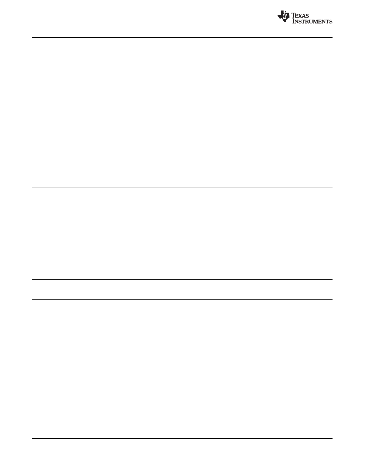
60
65
70
75
80
85
90
95
100
0 0.5 1 1.5 2 2.5 3 3.5
I -OutputCurrent- A
O
Efficiency-%
V =2.5V
O
V =5V
I
V =12V
I
V =15V
I
Product
Folder
Sample &
Buy
Technical
Documents
Tools &
Software
Support &
Community
SLVS875C –JANUARY 2009–REVISED NOVEMBER 2014
TPS54332 3.5-A, 28-V, 1-MHz, Step-Down DC-DC Converter With Eco-Mode™
1 Features 3 Description
1
• 3.5-V to 28-V Input Voltage Range
• Adjustable Output Voltage Down to 0.8 V
• Integrated 80-mΩ High-Side MOSFET Supports
up to 3.5-A Continuous Output Current
• High Efficiency at Light Loads With a PulseSkipping Eco-Mode™
• Fixed 1-MHz Switching Frequency
• Typical 1-μA Shutdown Quiescent Current
• Adjustable Slow-Start Limits Inrush Currents
• Programmable UVLO Threshold
• Overvoltage Transient Protection
• Cycle-by-Cycle Current Limit, Frequency Foldback
and Thermal Shutdown Protection
• Available in Thermally Enhanced 8-Pin SOIC
PowerPAD™ Package
• Supported by WEBENCH™ Tool
(http://www.ti.com/lsds/ti/analog/webench/overvie
w.page)
2 Applications
• Consumer Applications such as Set-Top Boxes,
CPE Equipment, LCD Displays, Peripherals, and
Battery Chargers
• Industrial and Car Audio Power Supplies
• 5-V, 12-V and 24-V Distributed Power Systems
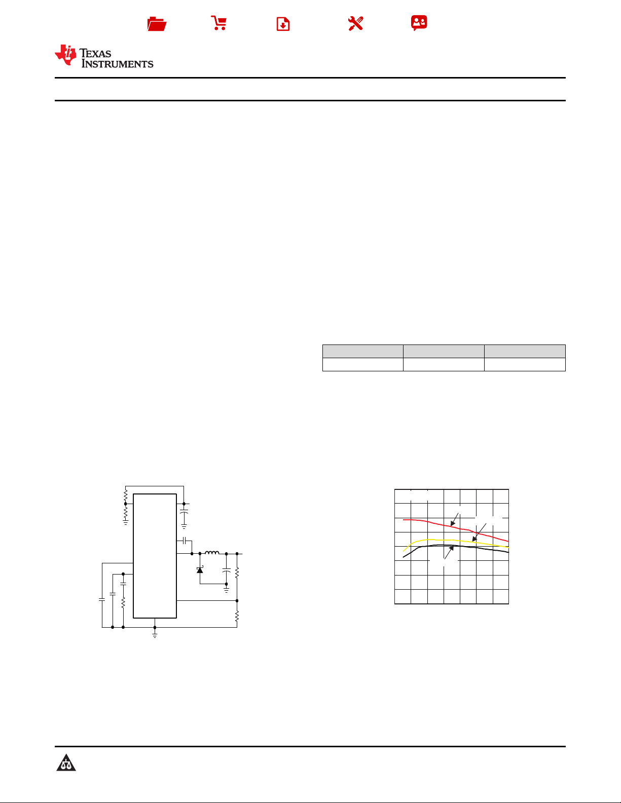
The TPS54332 is a 28-V, 3.5-A non-synchronous
buck converter that integrates a low-R
MOSFET. To increase efficiency at light loads, a
pulse-skipping Eco-Mode feature is automatically
activated. Furthermore, the 1-μA shutdown supply
current allows the device to be used in batterypowered applications. Current mode control with
internal slope compensation simplifies the external
compensation calculations and reduces component
count while allowing the use of ceramic output
capacitors. A resistor divider programs the hysteresis
of the input undervoltage lockout. An overvoltage
transient protection circuit limits voltage overshoots
during start-up and transient conditions. A cycle-bycycle current limit scheme, frequency foldback and
thermal shutdown protect the device and the load in
the event of an overload condition. The TPS54332 is
available in an 8-pin SOIC PowerPAD™ package.
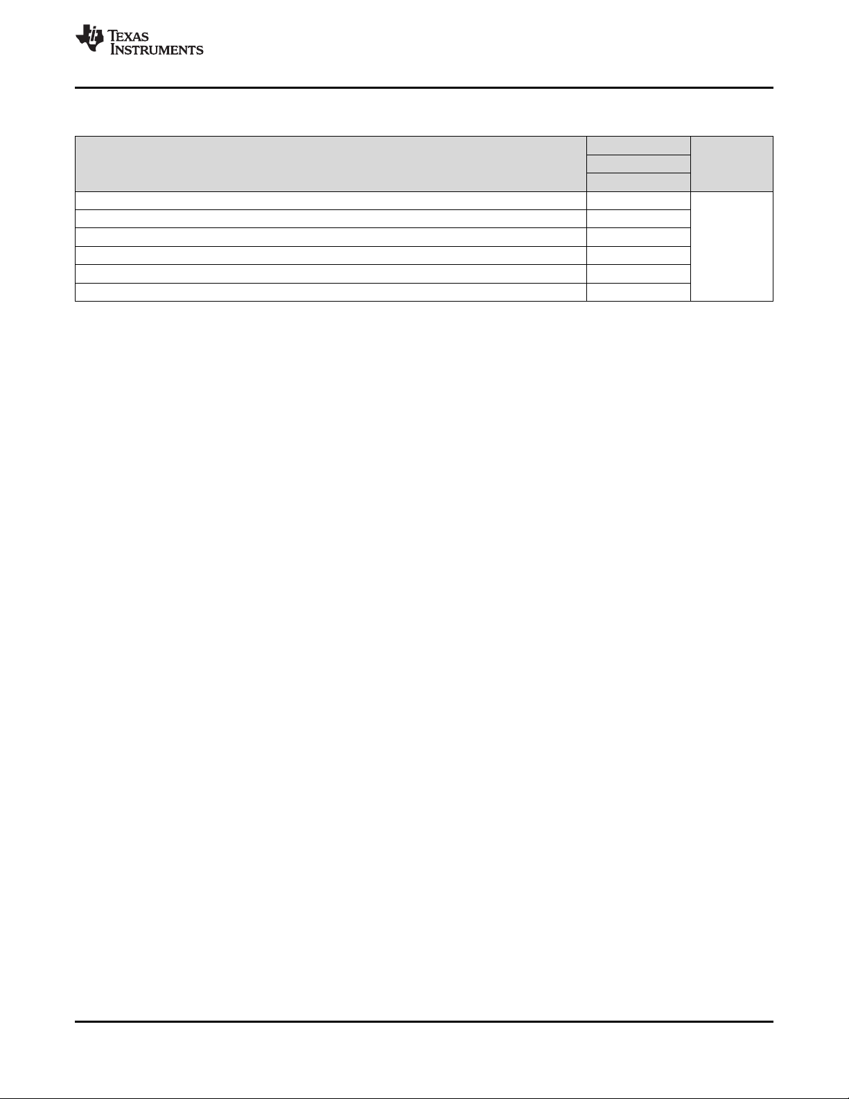
Device Information
PART NUMBER PACKAGE BODY SIZE (NOM)
TPS54332 SO PowerPAD (8) 4.90 mm× 3.90 mm
(1) For all available packages, see the orderable addendum at
the end of the datasheet.
DS(on)
(1)
TPS54332
high-side
1
An IMPORTANT NOTICE at the end of this data sheet addresses availability, warranty, changes, use in safety-critical applications,
intellectual property matters and other important disclaimers. PRODUCTION DATA.
Simplified Schematic Efficiency
TPS54332
SLVS875C –JANUARY 2009–REVISED NOVEMBER 2014
www.ti.com
Table of Contents
1 Features.................................................................. 1
2 Applications ........................................................... 1
3 Description............................................................. 1
4 Revision History..................................................... 2
5 Pin Configuration and Functions......................... 3
6 Specifications......................................................... 4
6.1 Absolute Maximum Ratings ...................................... 4
6.2 Handling Ratings....................................................... 4
6.3 Recommended Operating Conditions....................... 4
6.4 Thermal Information.................................................. 5
6.5 Electrical Characteristics........................................... 6
6.6 Switching Characteristics.......................................... 6
6.7 Typical Characteristics: Characterization Curves ..... 7
6.8 Typical Characteristics: Supplemental Application
Curves........................................................................ 8
7 Detailed Description .............................................. 9
7.1 Overview ................................................................... 9
7.2 Functional Block Diagram....................................... 10
7.3 Feature Description................................................. 10
7.4 Device Functional Modes........................................ 13
8 Application and Implementation ........................ 14
8.1 Application Information............................................ 14
8.2 Typical Application.................................................. 14
9 Power Supply Recommendations...................... 24
10 Layout................................................................... 24
10.1 Layout Guidelines ................................................. 24
10.2 Layout Example .................................................... 25
10.3 Estimated Circuit Area .......................................... 25
10.4 Electromagnetic Interference (EMI)
Considerations......................................................... 25
11 Device and Documentation Support ................. 26
11.1 Device Support...................................................... 26
11.2 Trademarks........................................................... 26
11.3 Electrostatic Discharge Caution............................ 26
11.4 Glossary................................................................ 26
12 Mechanical, Packaging, and Orderable
Information........................................................... 26
4 Revision History
NOTE: Page numbers for previous revisions may differ from page numbers in the current version.
Changes from Revision B (Feburary 2013) to Revision C Page
• Added Pin Configuration and Functions section, Handling Rating table, Feature Description section, Device
Functional Modes, Application and Implementation section, Power Supply Recommendations section, Layout
section, Device and Documentation Support section, and Mechanical, Packaging, and Orderable Information
section ................................................................................................................................................................................... 1
Changes from Revision A (January 2013) to Revision B Page
• Deleted Swift™ from the data sheet title................................................................................................................................ 1
• Deleted feature Item: For SWIFT™ Documentation, See the TI Website at www.ti.com/swift.............................................. 1
2 Submit Documentation Feedback Copyright © 2009–2014, Texas Instruments Incorporated
Product Folder Links: TPS54332
1
2
3
4
5
6
7
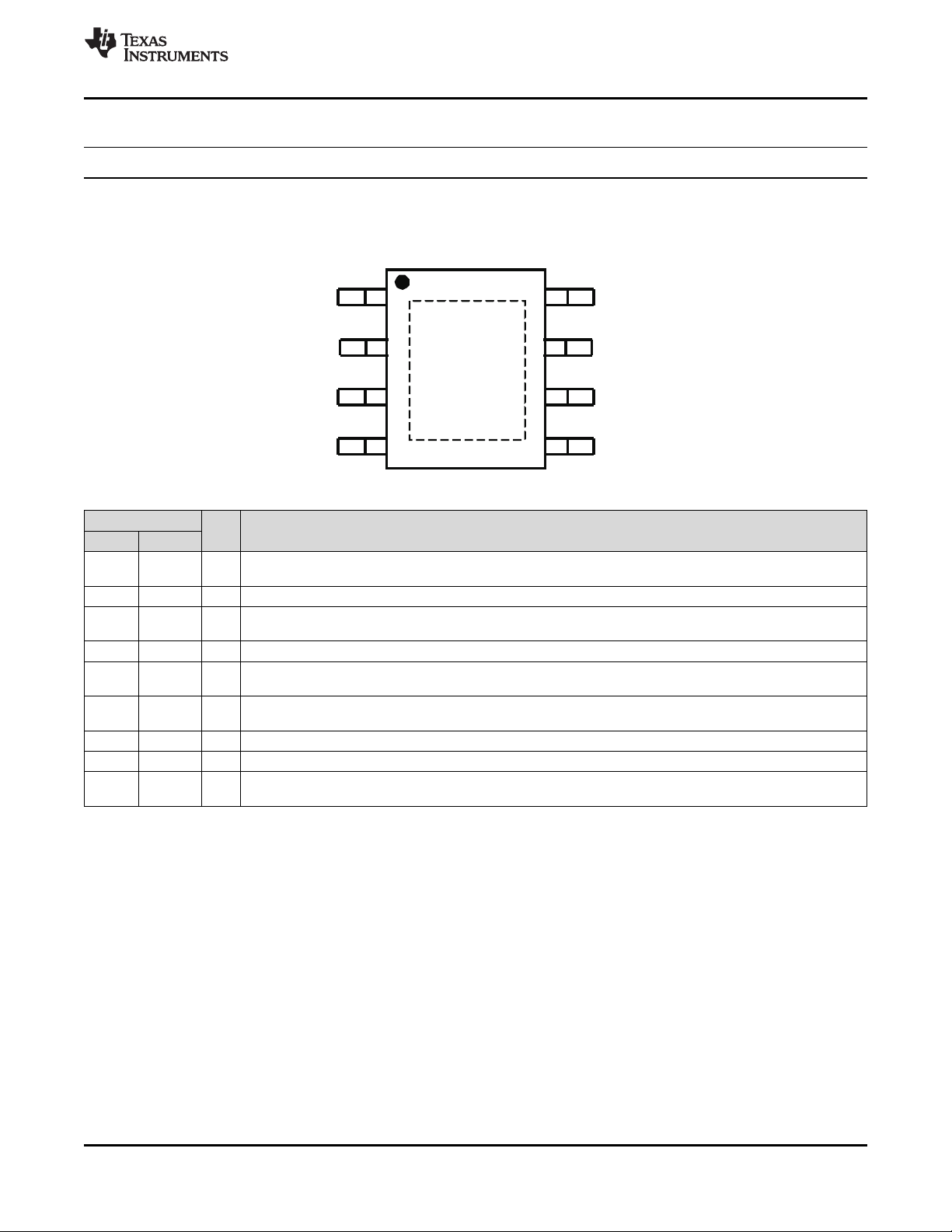
8BOOT
VIN
EN
SS
PH
GND
COMP
VSENSE
PowerPAD
(Pin 9)
DDA PACKAGE
(TOP VIEW)
TPS54332
www.ti.com
Changes from Original (March 2007) to Revision A Page
• Changed the ABSOLUTE MAXIMUM RATINGS table, Input Voltage - EN pin max value From: 5V to 6V.......................... 4
SLVS875C –JANUARY 2009–REVISED NOVEMBER 2014
5 Pin Configuration and Functions
Pin Functions
PIN I/O DESCRIPTION
NAME NO.
BOOT 1 O A 0.1-μF bootstrap capacitor is required between BOOT and PH. If the voltage on this capacitor falls below the
VIN 2 I Input supply voltage, 3.5 V to 28 V.
EN 3 I Enable pin. Pull below 1.25 V to disable. Float to enable. Programming the input undervoltage lockout with two
SS 4 I Slow-start pin. An external capacitor connected to this pin sets the output rise time.
VSENS 5 I Inverting node of the gm error amplifier.
E
COMP 6 O Error amplifier output, and input to the PWM comparator. Connect frequency compensation components to this
GND 7 - Ground.
PH 8 O The source of the internal high-side power MOSFET.
PowerP 9 - GND pin must be connected to the exposed pad for proper operation.
AD
minimum requirement, the high-side MOSFET is forced to switch off until the capacitor is refreshed.
resistors is recommended.
pin.
Copyright © 2009–2014, Texas Instruments Incorporated Submit Documentation Feedback 3
Product Folder Links: TPS54332
TPS54332
SLVS875C –JANUARY 2009–REVISED NOVEMBER 2014
www.ti.com
6 Specifications
6.1 Absolute Maximum Ratings
over operating free-air temperature range (unless otherwise noted)
Input Voltage VIN –0.3 30 V
EN –0.3 6
BOOT 38
VSENSE –0.3 3
COMP –0.3 3
SS –0.3 3
Output Voltage BOOT-PH 8 V
PH –0.6 30
PH (10 ns transient from ground to negative peak) –5
Source Current EN 100 μA
BOOT 100 mA
VSENSE 10 μA
PH 9.25 A
Sink Current VIN 9.25 A
COMP 100 μA
SS 200
Operating Junction –40 150 °C
Temperature
(1) Stresses beyond those listed under Absolute Maxmium Ratings may cause permanent damage to the device. These are stress ratings
only, which do not imply functional operation of the device at these or any other conditions beyond those indicated under Recommended
Operating Conditions. Exposure to absolute-maximum-rated conditions for extended periods may affect device reliability.
(1)
MIN MAX UNIT
6.2 Handling Ratings
MIN MAX UNIT
T
stg
V
(ESD)
(1) JEDEC document JEP155 states that 500-V HBM allows safe manufacturing with a standard ESD control process.
(2) JEDEC document JEP157 states that 250-V CDM allows safe manufacturing with a standard ESD control process.
Storage Temperature –65 150 °C
Electrostatic Discharge Human body model (HBM), per ANSI/ESDA/JEDEC JS- 2 kV
001, all pins
Charged device model (CDM), per JEDEC specification 500 V
JESD22-C101, all pins
(1)
(2)
6.3 Recommended Operating Conditions
over operating free-air temperature range (unless otherwise noted)
MIN MAX UNIT
Operating Input Voltage on (VIN pin) 3.5 28 V
Operating junction temperature, T
J
–40 150 °C
4 Submit Documentation Feedback Copyright © 2009–2014, Texas Instruments Incorporated
Product Folder Links: TPS54332
TPS54332
www.ti.com
SLVS875C –JANUARY 2009–REVISED NOVEMBER 2014
6.4 Thermal Information
TPS54332
THERMAL METRIC
R
θJA
R
θJC(top)
R
θJB
ψ
JT
ψ
JB
R
θJC(bot)
Junction-to-ambient thermal resistance 48.7
Junction-to-case (top) thermal resistance 52.4
Junction-to-board thermal resistance 25.3
Junction-to-top characterization parameter 8.4
Junction-to-board characterization parameter 25.2
Junction-to-case (bottom) thermal resistance 2.3
(1) For more information about traditional and new thermal metrics, see the IC Package Thermal Metrics application report, SPRA953.
(1)
HSOP UNIT
8 PINS
°C/W
Copyright © 2009–2014, Texas Instruments Incorporated Submit Documentation Feedback 5
Product Folder Links: TPS54332
TPS54332
SLVS875C –JANUARY 2009–REVISED NOVEMBER 2014
www.ti.com
6.5 Electrical Characteristics
TJ= –40°C to 150°C, VIN = 3.5 V to 28 V (unless otherwise noted)
DESCRIPTION TEST CONDITIONS MIN TYP MAX UNIT
SUPPLY VOLTAGE (VIN PIN)
Internal undervoltage lockout threshold Rising and Falling 3.5 V
Shutdown supply current EN = 0 V, VIN = 12 V, –40°C to 85°C 1 4 μA
Operating – non switching supply current VSENSE = 0.85 V 82 120 μA
ENABLE AND UVLO (EN PIN)
Enable threshold Rising and Falling 1.25 1.35 V
Input current Enable threshold – 50 mV -1 μA
Input current Enable threshold + 50 mV -4 μA
VOLTAGE REFERENCE
Voltage reference 0.772 0.8 0.828 V
HIGH-SIDE MOSFET
On resistance mΩ
ERROR AMPLIFIER
Error amplifier transconductance (gm) –2 μA < I
Error amplifier DC gain
Error amplifier unity gain bandwidth
(1)
(1)
Error amplifier source/sink current V
Switch current to COMP transconductance VIN = 12 V 12 A/V
PULSE-SKIPPING ECO-MODE
Pulse-skipping Eco-Mode switch current threshold 160 mA
CURRENT LIMIT
Current limit threshold VIN = 12 V 4.2 6.5 A
THERMAL SHUTDOWN
Thermal Shutdown 165 °C
SLOW-START (SS PIN)
Charge current V
SS to VSENSE matching V
(1) Specified by design
BOOT-PH = 3 V, VIN = 3.5 V 115 200
BOOT-PH = 6 V, VIN = 12 V 80 150
< 2 μA, V(COMP) = 1 V 92 μmhos
COMP
VSENSE = 0.8 V 800 V/V
5 pF capacitance from COMP to GND pins 2.7 MHz
= 1.0 V, 100-mV overdrive ±7 μA
(COMP)
= 0.4 V 2 μA
(SS)
= 0.4 V 10 mV
(SS)
6.6 Switching Characteristics
PARAMETERS TEST CONDITIONS MIN TYP MAX UNIT
TPS54332 Switching Frequency VIN = 12 V, 25°C 800 1000 1200 kHz
Minimum controllable on time VIN = 12 V, 25°C 110 135 ns
Maximum controllable duty ratio
(1) Specified by design
6 Submit Documentation Feedback Copyright © 2009–2014, Texas Instruments Incorporated
(1)
BOOT-PH = 6 V 90% 93%
Product Folder Links: TPS54332
9
9.5
10
10.5
11
11.5
12
12.5
13
13.5
14
-50 -25 0 25 50 75 100 125 150
Dmin-MinimumControllableDutyRatio-%
T -JunctionTemperature-°C
J
VIN=12V
90
100
110
120
130
140
-50 -25 0 25 50 75 100 125 150
Tonmin-MinimumControllableOnTime-ns
T -JunctionTemperature-°C
J
VIN=12V
980
990
1000
1010
1020
-50 -25 0 25 50 75 100 125 150
T -JunctionTemperature-°C
J
fsw-OscillatorFrequency-kHz
VIN=12V
0.776
0.782
0.788
0.794
0.8
0.806
0.812
0.818
0.824
-50 -25 0 25 50 75 100 125 150
Vref-VoltageReference-V
T -JunctionTemperature-°C
J
VIN=12V
0
2
4
6
8
3
8
13
18
23
28
V -InputVoltage-V
I
Isd-ShutdownCurrent- Am
T =150°C
J
T =-40°C
J
T =25°C
J
EN=0V
T -JunctionTemperature-°C
J
Rdson-OnResistance-mW
60
70
80
90
100
110
120
-50 -25 0 25 50 75 100 125 150
VIN=12V
www.ti.com
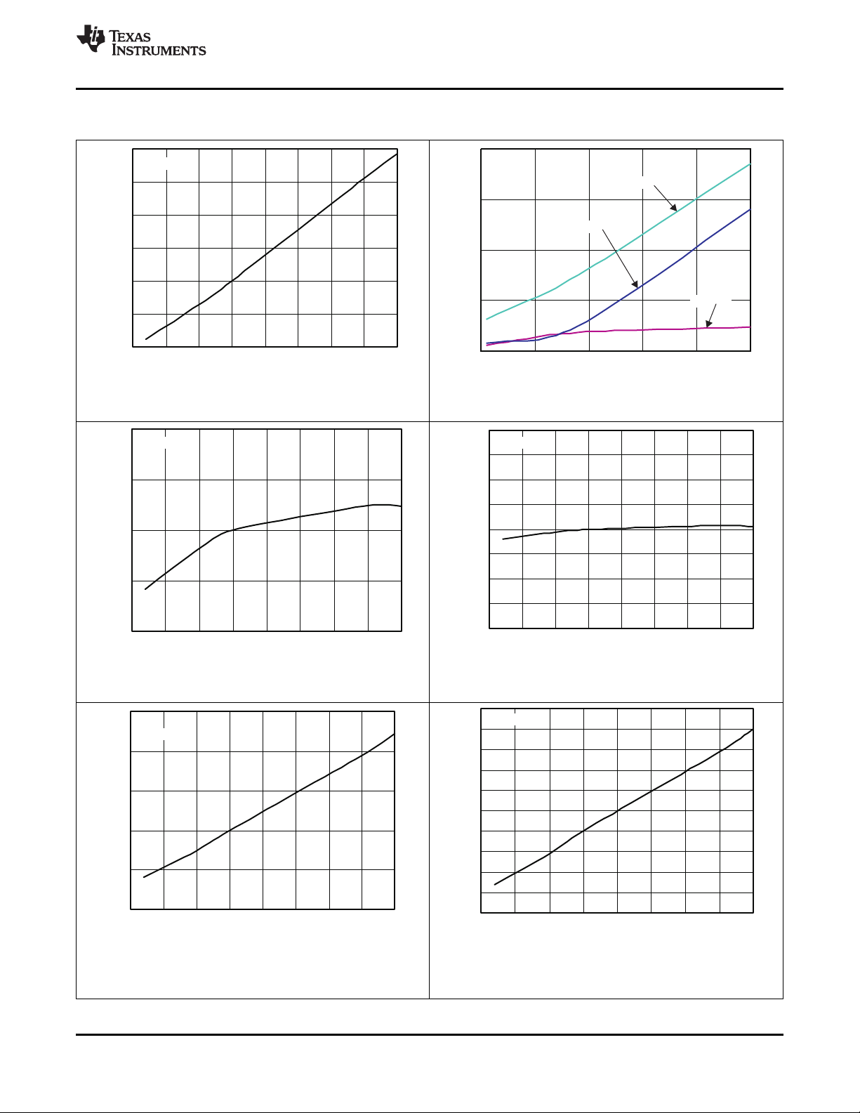
6.7 Typical Characteristics: Characterization Curves
TPS54332
SLVS875C –JANUARY 2009–REVISED NOVEMBER 2014
Figure 1. On Resistance vs Junction Temperature
Figure 3. Switching Frequency vs Junction Temperature
Figure 2. Shutdown Quiescent Current vs Input Voltage
Figure 4. Voltage Reference vs Junction Temperature
Copyright © 2009–2014, Texas Instruments Incorporated Submit Documentation Feedback 7
Figure 5. Minimum Controllable on Time vs Junction
Temperature
Figure 6. Minimum Controllable Duty Ratio vs Junction
Temperature
Product Folder Links: TPS54332
3
8
13
18
23 28
0.75
1.25
1.75
2.25
2.75
3.25
3.75
I =3.5 A
O
V -OutputVoltage-V
O
V -InputVoltage-V
I
3 8 13 18
23 28
0
5
10
15
20
25
30
I =3.5 A
O
V -InputVoltage-V
I
V -OutputVoltage-V
O
1.9
1.95
2
2.05
2.1
-50 -25 0 25 50 75 100 125 150
I -SSChargeCurrent- A
SS
m
T -JunctionTemperature-°C
J
VIN=12V
3
3.5
4
4.5
5
5.5
6
6.5
7
3 8 13 18 23 28
V -InputVoltage-V
I
CurrentLimitThreshold- A
T =150°C
J
T =-40°C
J
T =25°C
J
TPS54332
SLVS875C –JANUARY 2009–REVISED NOVEMBER 2014
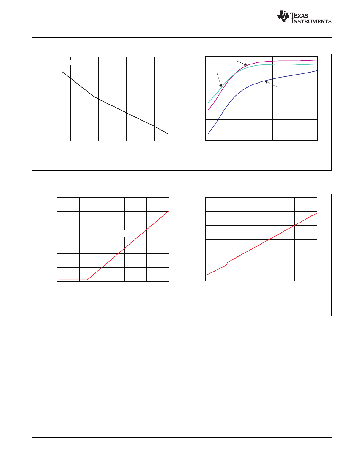
Typical Characteristics: Characterization Curves (continued)
www.ti.com
Figure 7. SS Charge Current vs Junction Temperature
Figure 8. Current Limit Threshold vs Input Voltage
6.8 Typical Characteristics: Supplemental Application Curves
Figure 9. Typical Minimum Output Voltage vs Input Voltage
Figure 10. Typical Maximum Output Voltage vs Input
Voltage
8 Submit Documentation Feedback Copyright © 2009–2014, Texas Instruments Incorporated
Product Folder Links: TPS54332

TPS54332
www.ti.com
SLVS875C –JANUARY 2009–REVISED NOVEMBER 2014
7 Detailed Description
7.1 Overview
The TPS54332 is a 28-V, 3.5-A, step-down (buck) converter with an integrated high-side, N-channel MOSFET.
To improve performance during line and load transients, the device implements a constant-frequency, current
mode control, which reduces output capacitance and simplifies external frequency compensation design. The
TPS54332 has a pre-set switching frequency of 1 MHz.
The TPS54332 needs a minimum input voltage of 3.5 V to operate normally. The EN pin has an internal pullup
current source that can be used to adjust the input voltage undervoltage lockout (UVLO) with two external
resistors. In addition, the pullup current provides a default condition when the EN pin is floating for the device to
operate. The operating current is 82 μA typically when not switching and under no load. When the device is
disabled, the supply current is 1 μA typically.
The integrated 80-mΩ high-side MOSFET allows for high-efficiency power supply designs with continuous output
currents up to 3.5 A.
The TPS54332 reduces the external component count by integrating the boot recharge diode. The bias voltage
for the integrated high-side MOSFET is supplied by an external capacitor on the BOOT to PH pin. The boot
capacitor voltage is monitored by an UVLO circuit and will turn the high-side MOSFET off when the voltage falls
below a preset threshold of 2.1 V typically. The output voltage can be stepped down to as low as the reference
voltage.
By adding an external capacitor, the slow-start time of the TPS54332 can be adjustable which enables flexible
output filter selection.
To improve the efficiency at light load conditions, the TPS54332 enters a special pulse-skipping Eco-Mode when
the peak inductor current drops below 160 mA typically.
The frequency foldback reduces the switching frequency during start-up and over current conditions to help
control the inductor current. The thermal shutdown gives the additional protection under fault conditions.
Copyright © 2009–2014, Texas Instruments Incorporated Submit Documentation Feedback 9
Product Folder Links: TPS54332
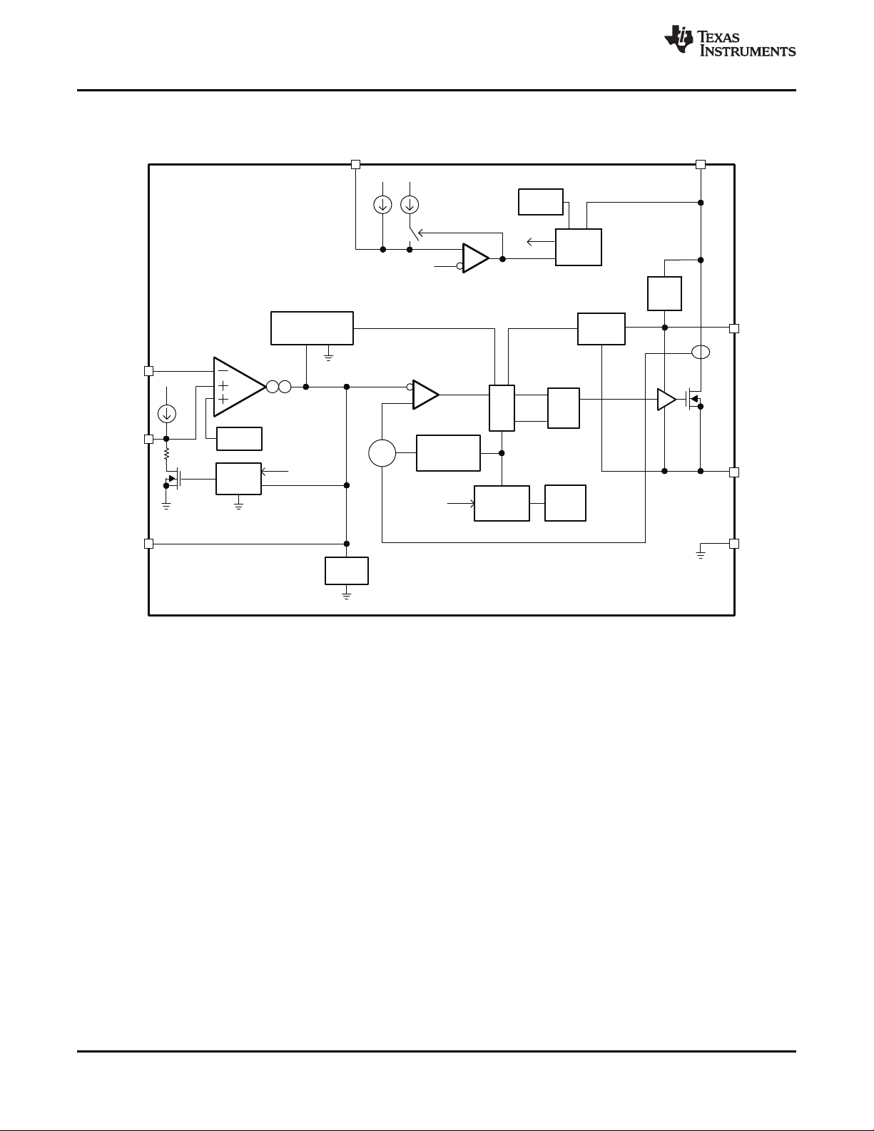
Error
Amplifier
RQ
S
Boot
Charge
Boot
UVLO
Current
Sense
Oscillator
Frequency
Shift
Gate
Drive
Logic
Slope
Compensation
PWM
Latch
PWM
Comparator
ECO-MODE
MinimumClamp
™
Maximum
Clamp
Voltage
Reference
Discharge
Logic
VSENSE
COMP
PH
BOOT
VIN
GND
Thermal
Shutdown
EN
Enable
Comparator
Shutdown
Logic
Shutdown
Enable
Threshold
S
1.25V
0.8V
80mW
165C
2.1V
12 A/V
SS
Shutdown
VSENSE
1 Am
3 Am
gm=92 A/V
DCgain=800V/V
BW=2.7MHz
m
2kW
2 Am
TPS54332
SLVS875C –JANUARY 2009–REVISED NOVEMBER 2014
7.2 Functional Block Diagram
www.ti.com
7.3 Feature Description
7.3.1 Fixed Frequency PWM Control
The TPS54332 uses a fixed-frequency, peak-current mode control. The internal switching frequency of the
TPS54332 is fixed at 1 MHz.
7.3.2 Voltage Reference (V
ref
The voltage reference system produces a ±2% initial accuracy voltage reference (±3.5% over temperature) by
scaling the output of a temperature stable band-gap circuit. The typical voltage reference is designed at 0.8 V.
7.3.3 Bootstrap Voltage (BOOT)
The TPS54332 has an integrated boot regulator and requires a 0.1-μF ceramic capacitor between the BOOT and
)
PH pin to provide the gate drive voltage for the high-side MOSFET. A ceramic capacitor with an X7R or X5R
grade dielectric is recommended because of the stable characteristics over temperature and voltage. To improve
dropout, the TPS54332 is designed to operate at 100% duty cycle as long as the BOOT to PH pin voltage is
greater than 2.1 V typically.
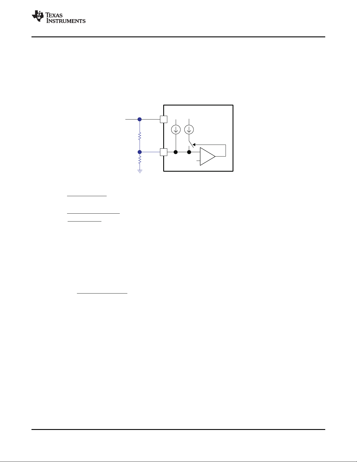
7.3.4 Enable and Adjustable Input Undervoltage Lockout (VIN UVLO)
The EN pin has an internal pullup current source that provides the default condition of the TPS54332 operating
when the EN pin floats.
10 Submit Documentation Feedback Copyright © 2009–2014, Texas Instruments Incorporated
Product Folder Links: TPS54332
( )
( ) ( )
( )
SS ref
SS
SS
C nF V V
T ms =
I A
´
m
EN
START EN
V
Ren2 =
V - V
+ 1 A
Ren1
m
START STOP
V - V
Ren1 =
3 Am
EN
1.25V
VIN
+
-
Ren1
Ren2
TPS54332
1 Am 3 Am
TPS54332
www.ti.com
SLVS875C –JANUARY 2009–REVISED NOVEMBER 2014
Feature Description (continued)
The TPS54332 is disabled when the VIN pin voltage falls below internal VIN UVLO threshold. TI recommends
using an external VIN UVLO to add Hysteresis unless VIN is greater than (V
with Hysteresis, use the external circuitry connected to the EN pin as shown in Figure 11. Once the EN pin
voltage exceeds 1.25 V, an additional 3 μA of hysteresis is added. Use Equation 1 and Equation 2 to calculate
the resistor values needed for the desired VIN UVLO threshold voltages. The V
voltage, the V
V
should always be greater than 3.5 V.
STOP
is the input stop threshold voltage and the VENis the enable threshold voltage of 1.25 V. The
STOP
Figure 11. Adjustable Input Undervoltage Lockout
+ 2 V). To adjust the VIN UVLO
OUT
is the input start threshold
START
(1)
(2)
7.3.5 Programmable Slow-Start Using SS Pin
TI highly recommends programing the slow-start time externally because no slow-start time is implemented
internally. The TPS54332 effectively uses the lower voltage of the internal voltage reference or the SS pin
voltage as the power supply’s reference voltage fed into the error amplifier and will regulate the output
accordingly. A capacitor (CSS) on the SS pin-to-ground implements a slow-start time. The TPS54332 has an
internal pullup current source of 2 μA that charges the external slow-start capacitor. The equation for the slowstart time (10% to 90%) is shown in Equation 3 . The V
is 0.8V and the ISScurrent is 2 μA.
ref
(3)
The slow-start time should be set between 1 ms to 10 ms to ensure good start-up behavior. The slow-start
capacitor should be no more than 27 nF.
If during normal operation, the input voltage drops below the VIN UVLO threshold, or the EN pin is pulled below
1.25 V, or a thermal shutdown event occurs, the TPS54332 stops switching.
7.3.6 Error Amplifier
The TPS54332 has a transconductance amplifier for the error amplifier. The error amplifier compares the
VSENSE voltage to the internal effective voltage reference presented at the input of the error amplifier. The
transconductance of the error amplifier is 92 μA/V during normal operation. Frequency compensation
components are connected between the COMP pin and ground.
7.3.7 Slope Compensation
In order to prevent the sub-harmonic oscillations when operating the device at duty cycles greater than 50%, the
TPS54332 adds a built-in slope compensation which is a compensating ramp to the switch current signal.
Copyright © 2009–2014, Texas Instruments Incorporated Submit Documentation Feedback 11
Product Folder Links: TPS54332

TPS54332
SLVS875C –JANUARY 2009–REVISED NOVEMBER 2014
www.ti.com
Feature Description (continued)
7.3.8 Current Mode Compensation Design
To simplify design efforts using the TPS54332, the typical designs for common applications are listed in Table 1.
For designs using ceramic output capacitors, proper derating of ceramic output capacitance is recommended
when doing the stability analysis. This is because the actual ceramic capacitance drops considerably from the
nominal value when the applied voltage increases. Advanced users may refer to the Detailed Design Procedure
in the Application and Implementation section for the detailed guidelines, or use the WEBENCH tool
(http://www.ti.com/lsds/ti/analog/webench/overview.page).
Table 1. Typical Designs (Referring to Simplified Schematic on Page 1)
VIN V
(V) (V) (kHz) (μH) (kΩ) (kΩ) (pF) (pF) (kΩ)
12 5 1000 3.3 Ceramic 22-μF 10 1.91 18 470 24.9
12 3.3 1000 2.7 Ceramic 22-μF x 2 10 3.24 18 1800 39.2
12 5 1000 3.3 Aluminum 330-μF / 160-mohm 10 1.91 22 47 10
12 3.3 1000 2.7 Aluminum 330-μF / 160-mohm 10 3.24 39 100 29.4
OUT
7.3.9 Overcurrent Protection and Frequency Shift
The TPS54332 implements current mode control that uses the COMP pin voltage to turn off the high-side
MOSFET on a cycle-by-cycle basis. Every cycle, the switch current and the COMP pin voltage are compared;
when the peak inductor current intersects the COMP pin voltage, the high-side switch is turned off. During
overcurrent conditions that pull the output voltage low, the error amplifier responds by driving the COMP pin high,
causing the switch current to increase. The COMP pin has a maximum clamp internally, which limit the output
current.
The TPS54332 provides robust protection during short circuits. There is potential for overcurrent runaway in the
output inductor during a short circuit at the output. The TPS54332 solves this issue by increasing the off-time
during short circuit conditions by lowering the switching frequency. The switching frequency is divided by 8, 4, 2,
and 1 as the voltage ramps from 0 V to 0.8 V on VSENSE pin. The relationship between the switching frequency
and the VSENSE pin voltage is shown in Table 2.
F
sw
L
o
C
o
R
R
O1
O2
C
C
2
1
R
3
Table 2. Switching Frequency Conditions
SWITCHING FREQUENCY VSENSE PIN VOLTAGE
1 MHz VSENSE ≥ 0.6 V
1 MHz / 2 0.6 V > VSENSE ≥ 0.4 V
1 MHz / 4 0.4 V > VSENSE ≥ 0.2 V
1 MHz / 8 0.2 V > VSENSE
7.3.10 Overvoltage Transient Protection
The TPS54332 incorporates an overvoltage transient protection (OVTP) circuit to minimize output voltage
overshoot when recovering from output fault conditions or strong unload transients. The OVTP circuit includes an
overvoltage comparator to compare the VSENSE pin voltage and internal thresholds. When the VSENSE pin
voltage goes above 109% × V
below 107% × V
, the high-side MOSFET will be enabled again.
ref
, the high-side MOSFET will be forced off. When the VSENSE pin voltage falls
ref
7.3.11 Thermal Shutdown
The device implements an internal thermal shutdown to protect itself if the junction temperature exceeds 165°C.
The thermal shutdown forces the device to stop switching when the junction temperature exceeds the thermal
trip threshold. Once the die temperature decreases below 165°C, the device reinitiates the power-up sequence.
12 Submit Documentation Feedback Copyright © 2009–2014, Texas Instruments Incorporated
Product Folder Links: TPS54332

TPS54332
www.ti.com
SLVS875C –JANUARY 2009–REVISED NOVEMBER 2014
7.4 Device Functional Modes
7.4.1 Operation With VIN < 3.5 V
The device is recommended to operate with input voltages above 3.5 V. The typical VIN UVLO threshold is not
specified and the device may operate at input voltages down to the UVLO voltage. At input voltages below the
actual UVLO voltage, the device will not switch. If EN is externally pulled up or left floating, when VIN passes the
UVLO threshold the device will become active. Switching will commenced when the soft-start sequence is
initiated.
7.4.2 Operation With EN Control
The enable threshold voltage is 1.25 V typical. With EN held below that voltage the device is disabled and
switching is inhibited even if VIN is above its UVLO threshold. The IC quiescent current is reduced in this state. If
the EN voltage is increased above the threshold while VIN is above its UVLO threshold, the device becomes
active. Switching is enabled, and the slow-start sequence is initiated.
7.4.3 Eco-Mode
The device is designed to operate in pulse-skipping Eco-Mode at light-load currents to boost light-load efficiency.
When the peak inductor current is lower than pulse skip threshold, the COMP pin voltage falls to 0.5 V (typical)
and the device enters Eco-Mode . When the device is in Eco-Mode, the COMP pin voltage is clamped at 0.5 V
internally which prevents the high-side integrated MOSFET from switching. The peak inductor current must rise
above 160 mA for the COMP pin voltage to rise above 0.5 V and exit Eco-Mode. Because the integrated current
comparator catches the peak inductor current only, the average load current entering Eco-Mode varies with the
applications and external output filters.
Copyright © 2009–2014, Texas Instruments Incorporated Submit Documentation Feedback 13
Product Folder Links: TPS54332

TPS54332
SLVS875C –JANUARY 2009–REVISED NOVEMBER 2014
www.ti.com
8 Application and Implementation
NOTE
Information in the following applications sections is not part of the TI component
specification, and TI does not warrant its accuracy or completeness. TI’s customers are
responsible for determining suitability of components for their purposes. Customers should
validate and test their design implementation to confirm system functionality.
8.1 Application Information
The TPS54332 is typically used as step down converters, which convert a voltage from 3.5 V - 28 V to a lower
voltage. WEBENCH software is available to aid in the design and analysis of circuits.
TPS54231 TPS54232 TPS54233 TPS54331 TPS54332
IO(Max) 2 A 2 A 2 A 3 A 3.5 A
Input Voltage Range 3.5 V - 28 V 3.5 V - 28 V 3.5 V - 28 V 3.5 V - 28 V 3.5 V - 28 V
Switching Freq. (Typ) 570 kHz 1000 kHz 285 kHz 570 kHz 1000 kHz
Switch Current Limit (Min) 2.3 A 2.3 A 2.3 A 3.5 A 4.2 A
Pin/Package 8/SOIC 8/SOIC 8/SOIC 8/SOIC 8/SO PowerPAD™
8.2 Typical Application
Figure 12. Typical Application Schematic
8.2.1 Design Requirements
For this design example, use the following as the input parameters:
DESIGN PARAMETER EXAMPLE VALUE
Input voltage range 5 V to 15 V
Output voltage 2.5 V
Input ripple voltage 200 mV
Output ripple voltage 20 mV
Output current rating 3.5 A
Operating Frequency 1 MHz
14 Submit Documentation Feedback Copyright © 2009–2014, Texas Instruments Incorporated
Product Folder Links: TPS54332

( )
OUT(MAX)
IN OUT(MAX) MAX
BULK SW
I 0.25
V = + I ESR
C f
´
D ´
´
OUT REF
R5
V = V +1
R6
é ù
´
ê ú
ë û
REF
OUT REF
R5 V
R6 =
V V
´
-
TPS54332
www.ti.com
SLVS875C –JANUARY 2009–REVISED NOVEMBER 2014
8.2.2 Detailed Design Procedure
The following design procedure can be used to select component values for the TPS54332. Alternately, the
WEBENCH Tool may be used to generate a complete design. The WEBENCH Tool uses an iterative design
procedure and accesses a comprehensive database of components when generating a design. This section
presents a simplified discussion of the design process.
8.2.2.1 Switching Frequency
The switching frequency for the TPS54332 is fixed at 1 MHz.
8.2.2.2 Output Voltage Set Point
The output voltage of the TPS54332 is externally adjustable using a resistor divider network. In the application
circuit of Figure 12, this divider network is comprised of R5 and R6. The relationship of the output voltage to the
resistor divider is given by Equation 4 and Equation 5.
(4)
(5)
Choose R5 to be approximately 10 kΩ. Slightly increasing or decreasing R5 can result in closer output voltage
matching when using standard value resistors. In this design, R4 = 10.2 kΩ and R = 4.75 kΩ, resulting in a 2.5-V
output voltage.
8.2.2.3 Input Capacitors
The TPS54332 requires an input decoupling capacitor and depending on the application, a bulk-input capacitor.
The typical recommended value for the decoupling capacitor is 10 μF. A high-quality ceramic type X5R or X7R is
recommended. The voltage rating should be greater than the maximum input voltage. A smaller value may be
used as long as all other requirements are met; however 10 μF has been shown to work well in a wide variety of
circuits. Additionally, some bulk capacitance may be needed, especially if the TPS54332 circuit is not located
within about 2 inches from the input voltage source. The value for this capacitor is not critical but should be rated
to handle the maximum input voltage including ripple voltage, and should filter the output so that input ripple
voltage is acceptable. For this design, a single 10-μF capacitor is used for the input decoupling capacitor. It is
X5R dielectric rated for 25 V. The equivalent series resistance (ESR) is approximately 3 mΩ, and the current
rating is 3 A.
This input ripple voltage can be approximated by Equation 6.
(6)
Where I
OUT(MAX)
the bulk capacitor value and ESR
is the maximum load current, fSWis the switching frequency (derated by a factor of 0.8), C
is the maximum series resistance of the bulk capacitor.
MAX
BULK
is
The maximum RMS imput ripple current also needs to be checked. For worst case conditions, this can be
approximated by Equation 7.
(7)
In this case, the input ripple voltage would be 98 mV and the RMS ripple current would be 1.75 A. It is also
important to note that the actual input voltage ripple will be greatly affected by parasitic associated with the layout
and the output impedance of the voltage source. The actual input voltage ripple for this circuit is shown in Design
Parameters and is larger than the calculated value. This measured value is still below the specified input limit of
200 mV. The maximum voltage across the input capacitors would be VIN max plus ΔVIN/2. The chosen bypass
capacitor is rated for 25 V and the ripple current capacity is greater than 3 A, providing ample margin. It is
important that the maximum ratings for voltage and current are not exceeded under any circumstance.
Copyright © 2009–2014, Texas Instruments Incorporated Submit Documentation Feedback 15
Product Folder Links: TPS54332
( )
´ -
´ ´ ´
OUT IN(MAX) OUT
L(PK) OUT(MAX)
IN(MAX) OUT SW
V V V
I = I +
1.6 V L F
( )
æ ö
´ -
ç ÷
´
ç ÷
´ ´ ´
è ø
2
OUT IN(MAX) OUT
2
L(RMS) OUT(MAX)
IN(MAX) OUT SW
V V V
1
I = I +
12 V L F 0.8
( )
OUT IN(MAX) OUT
LPP
IN(MAX) OUT SW
V × V V
V × L ƒ 0.8
-
´ ´
( )
0.8
´ -
´ ´ ´ ´
OUT(MAX) IN(MAX) OUT
MIN
IN(MAX) IND OUT SW
V V V
L =
V K I F
TPS54332
SLVS875C –JANUARY 2009–REVISED NOVEMBER 2014
www.ti.com
8.2.2.4 Output Filter Components
Two components need to be selected for the output filter, the output inductor L1 and the output capacitance.
Since the TPS54332 is an externally compensated device, a wide range of filter component types and values can
be supported.
8.2.2.5 Inductor Selection
To calculate the minimum value of the output inductor, use Equation 8.
(8)
K
is a coefficient that represents the amount of inductor ripple current relative to the maximum output current.
IND
In general, this value is at the discretion of the designer; however, the following guidelines may be used. For
designs using low-ESR output capacitors such as ceramics, a value as high as K
using higher ESR output capacitors, K
For this design example, use K
IND
= 0.2 yields better results.
IND
= 0.3 and the minimum inductor value is calculated to be 2.48 μH. For this
= 0.4 may be used. When
IND
design, a l 2.5-μH inductor is chosen.
For the output filter inductor, it is important that the RMS current and saturation current ratings not be exceeded.
The peak-to-peak inductor current is calculated using Equation 9.
(9)
The RMS inductor current can be found from Equation 10.
(10)
And the peak inductor current can be determined with Equation 11.
(11)
(12)
For this design, the RMS inductor current is 3.51 A and the peak inductor current is 4.15 A. The chosen inductor
is a Coilcraft MSS1038-252NX_ 2.5-μH. It has a saturation current rating of 7.62 A and an RMS current rating of
6.55 A, meeting these requirements. Smaller or larger inductor values can be used depending on the amount of
ripple current the designer wishes to allow so long as the other design requirements are met. Larger value
inductors will have lower AC current and result in lower output voltage ripple, while smaller inductor values will
increase ac current and output voltage ripple. In general, inductor values for use with the TPS54332 are in the
range of 1 μH to 47 μH.
8.2.2.6 Capacitor Selection
The important design factors for the output capacitor are DC voltage rating, ripple current rating, and equivalent
series resistance (ESR). The DC voltage and ripple current ratings cannot be exceeded. The ESR is important
because along with the inductor current it determines the amount of output ripple voltage. The actual value of the
output capacitor is not critical, but some practical limits do exist. Consider the relationship between the desired
closed-loop crossover frequency of the design and LC corner frequency of the output filter. In general, it is
desirable to keep the closed-loop crossover frequency at less than 1/5 of the switching frequency. With highswitching frequencies such as the 1 MHz frequency of this design, internal circuit limitations of the TPS54332
limit the practical maximum crossover frequency to about 75 kHz. In general, the closed-loop crossover
frequency should be higher than the corner frequency determined by the load impedance and the output
capacitor. This limits the minimum capacitor value for the output filter to:
16 Submit Documentation Feedback Copyright © 2009–2014, Texas Instruments Incorporated
Product Folder Links: TPS54332

ggm REF
DC
O
V V
G =
V
´
( )
12
OUT IN(MAX) OUT
COUT(RMS)
IN(MAX) OUT SW C
V × V V
1
I = ×
V × L × F × N
æ ö
-
ç ÷
ç ÷
è ø
( )
OPPMAX
max
LPP SW O
D 0.5
V
ESR =
I 4 F C
-
´ ´
ú
û
ù
ê
ë
é
+
´´
-
=
ESR
OSW
LP POPP
R
CF
D
IV
4
)5.0(
)2/(1
max_min_ COOO
FRC ´´´= p
TPS54332
www.ti.com
Where ROis the output load impedance (VO/IO) and fCOis the desired crossover frequency. For a desired
maximum crossover of 75 kHz the minimum value for the output capacitor is around 3.2 μF. This may not satisfy
the output ripple voltage requirement. The output ripple voltage consists of two components; the voltage change
due to the charge and discharge of the output filter capacitance and the voltage change due to the ripple current
times the ESR of the output filter capacitor. The output ripple voltage can be estimated by:
Where COis the total effective output capacitance.
The maximum ESR of the output capacitor can be determined from the amount of allowable output ripple as
specified in the initial design parameters. The contribution to the output ripple voltage due to ESR is the inductor
ripple current times the ESR of the output filter, so the maximum specified ESR as listed in the capacitor data
sheet is given by Equation 15.
Where V
output capacitor is given by Equation 16.
OPPMAX
is the desired maximum peak-to-peak output ripple. The maximum RMS ripple current in the
SLVS875C –JANUARY 2009–REVISED NOVEMBER 2014
(13)
(14)
(15)
(16)
The minimum switching frequency should be used in the above equations (derated by a factor of 0.8). For this
design example, two 47-μF ceramic output capacitors are chosen for C2 and C3. These are rated at 10 V with a
maximum ESR of 3 mΩ and a ripple current rating in excess of 3 A. The calculated total RMS ripple current is
300 mA (150 mA each) and the total ESR required is 20 mΩ or less. These output capacitors exceed the
requirements by a wide margin and will result in a reliable, high-performance design. it is important to note that
the actual capacitance in circuit may be less than the catalog value when the output is operating at the desired
output of 2.5 V. 10-V rated capacitors are used to minimize the this reduction in capacitance due to dc voltage on
the output. The selected output capacitor must be rated for a voltage greater than the desired output voltage plus
½ the ripple voltage. Any derating amount must also be included. Other capacitor types work well with the
TPS54332, depending on the needs of the application.
8.2.2.7 Compensation Components
The external compensation used with the TPS54332 allows for a wide range of output filter configurations. A
large range of capacitor values and types of dielectric are supported. The design example uses ceramic X5R
dielectric output capacitors, but other types are supported.
A Type II compensation scheme is recommended for the TPS54332. The compensation components are chosen
to set the desired closed-loop crossover frequency and phase margin for output filter components. The type II
compensation has the following characteristics; a DC gain component, a low-frequency pole, and a midfrequency zero or pole pair.
The DC gain is determined by Equation 17.
(17)
Where:
V
= 800
ggm
V
= 0.8 V
REF
The low-frequency pole is determined by Equation 18.
Copyright © 2009–2014, Texas Instruments Incorporated Submit Documentation Feedback 17
Product Folder Links: TPS54332

kFF
COP´=1
k
F
F
CO
Z=1
÷
ø
ö
ç
è
æ
+= deg45
2
tan
PB
k
( )
90degPB = PM PL- -
( ) ( )
10a ap p´ ´ ´ ´ - ´ ´ ´ ´ -
CO ESR O CO O O
PL = tan 2 F R C tan 2 F R C dB
( )
SENSE CO O
Gain = 20 log 2 R F Cp- ´ ´ ´ ´
( )
P1 Z P
F = 1/ 2 R Cp´ ´ ´
( )
Z1 Z Z
F = 1/ 2 R Cp´ ´ ´
( )
p´ ´ ´
PO OO Z
F = 1/ 2 R C
TPS54332
SLVS875C –JANUARY 2009–REVISED NOVEMBER 2014
ROA= 8.696 MΩ.
The mid-frequency zero is determined by Equation 19.
And, the mid-frequency pole is given by Equation 20.
The first step is to choose the closed-loop crossover frequency. The closed-loop crossover frequency should be
less than 1/8 of the minimum operating frequency, but for the TPS54332 it is recommended that the maximum
closed-loop crossover frequency be not greater than 75 kHz. Next, the required gain and phase boost of the
crossover network needs to be calculated. By definition, the gain of the compensation network must be the
inverse of the gain of the modulator and output filter. For this design example, where the ESR zero is much
higher than the closed-loop crossover frequency, the gain of the modulator and output filter can be approximated
by Equation 21.
Where:
R
FCO= Closed-loop crossover frequency
CO= Output capacitance
The phase loss is given by Equation 22.
SENSE
= 1 Ω / 12
www.ti.com
(18)
(19)
(20)
(21)
(22)
Where:
R
= Equivalent series resistance of the output capacitor
ESR
RO= VO/I
The measured overall loop response for the circuit is given in Figure 20. Note that the actual closed-loop
crossover frequency is higher than intended at about 25 kHz. This is primarily due to variation in the actual
values of the output filter components and tolerance variation of the internal feed-forward gain circuitry. Overall
the design has greater than 60 degrees of phase margin and will be completely stable over all combinations of
line and load variability.
Now that the phase loss is known the required amount of phase boost to meet the phase margin requirement
can be determined. The required phase boost is given by Equation 23.
Where PM = the desired phase margin.
A zero / pole pair of the compensation network will be placed symmetrically around the intended closed-loop
frequency to provide maximum phase boost at the crossover point. The amount of separation can be determined
by Equation 24 and the resultant zero and pole frequencies are given by Equation 25 and Equation 26.
O
(23)
(24)
(25)
18 Submit Documentation Feedback Copyright © 2009–2014, Texas Instruments Incorporated
Product Folder Links: TPS54332
(26)

1
Cp
p´ ´ ´
= = 9.8 pF
2 216000 75000
1
Cz
p´ ´ ´
= = 183 pF
2 11570 75000
p´ ´ ´ ´ ´ ´ ´
W
´ ´
-6 6
2 50000 2.5 82 10 8.696 10
Rz = = 72.92 k
12 800 0.8
zP
P
RFC´´´
=
1
21p
zZ
Z
RFC´´´
=
1
21p
CO O O OA
Z
ICOMP ggm REF
2 × × F × V × C × R
R =
GM × V × V
p
TPS54332
www.ti.com
SLVS875C –JANUARY 2009–REVISED NOVEMBER 2014
The low-frequency pole is set so that the gain at the crossover frequency is equal to the inverse of the gain of the
modulator and output filter. Due to the relationships established by the pole and zero relationships, the value of
RZcan be derived directly by Equation 27 .
(27)
Where:
VO= Output voltage
CO= Output capacitance
FCO= Desired crossover frequency
ROA= 8.696 MΩ
GM
V
ggm
V
REF
COMP
= 800
= 0.8 V
= 12 A/V
With RZknown, CZand CPcan be calculated using Equation 28 and Equation 29.
(28)
(29)
For this design, the two 47-μF output capacitors are used. For ceramic capacitors, the actual output capacitance
is less than the rated value when the capacitors have a DC bias voltage applied. This is the case in a dc/dc
converter. The actual output capacitance may be as low as 54 μF. The combined ESR is approximately .001 Ω.
Using Equation 21 and Equation 22, the output stage gain and phase loss are equivalent as:
Gain = –6.94 dB
and
PL - –93.94 degrees
For 70 degrees of phase margin, Equation 23 requires 63.64 degrees of phase boost.
Equation 24, Equation 25, and Equation 26 are used to find the zero and pole frequencies of:
FZ1= 11.57 kHz
And
FP1= 216 kHz
RZ, CZ, and CPare calculated using Equation 27, Equation 28, and Equation 29.
(30)
(31)
Using standard values for R3, C6, and C7 in the application schematic of Figure 12.
R3 = 75 kΩ
C6 = 180 pF
C7 = 10 pF
Copyright © 2009–2014, Texas Instruments Incorporated Submit Documentation Feedback 19
Product Folder Links: TPS54332
(32)

V = 0.118 x ((V - I x R + V ) - I x R ) - V
O(min) IN(max) Omin DS(on) max) D O(min) L D
V = 0.91 x ((V – I x R ) + V ) – (I x R ) – V
O(max) IN(min) O(max) DS(on) max D O(max) L D
TPS54332
SLVS875C –JANUARY 2009–REVISED NOVEMBER 2014
www.ti.com
8.2.2.8 Bootstrap Capacitor
Every TPS54332 design requires a bootstrap capacitor, C4. The bootstrap capacitor must be 0.1 μF. The
bootstrap capacitor is located between the PH pins and BOOT pin. The bootstrap capacitor should be a highquality, ceramic type with X7R or X5R grade dielectric for temperature stability.
8.2.2.9 Catch Diode
The TPS54332 is designed to operate using an external catch diode between PH and GND. The selected diode
must meet the absolute maximum ratings for the application: Reverse voltage must be higher than the maximum
voltage at the PH pin, which is Vin(max) + 0.5 V. Peak current must be greater than IOUTMAX plus on half the
peak-to-peak inductor current. Forward-voltage drop should be small for higher efficiencies. It is important to note
that the catch diode conduction time is typically longer than the high-side FET on time, so attention paid to diode
parameters can make a marked improvement in overall efficiency. Additionally, check that the device chosen is
capable of dissipating the power losses. For this design, a Diodes, Inc. B340A is chosen, with a reverse voltage
of 40 V, forward current of 3 A, and a forward voltage drop of 0.5 V.
8.2.2.10 Output Voltage Limitations
Due to the internal design of the TPS54332, there are both upper and lower output voltage limits for any given
input voltage. The upper limit of the output voltage set point is constrained by the maximum duty cycle of 91%
and is given by Equation 33.
(33)
Where:
V
I
= Minimum input voltage
IN(min)
= Maximum load current
O(max)
VD= Catch diode forward voltage
RL= Output inductor series resistance
The equation assumes maximum on resistance for the internal high-side FET.
The lower limit is constrained by the minimum controllable on time which may be as high as 130 ns. The
approximate minimum output voltage for a given input voltage and minimum load current is given by Equation 32.
(34)
Where:
V
I
O(min)
= Maximum input voltage
IN(max)
= Minimum load current
VD= Catch diode forward voltage
RL= Output inductor series resistance
This equation assumes nominal on-resistance for the high-side FET and accounts for worst case variation of
operating frequency set point. Any design operating near the operational limits of the device should be carefully
checked to assure proper functionality.
8.2.2.11 Power Dissipation Estimate
The following formulas show how to estimate the device power dissipation under continuous conduction mode
operations. They should not be used if the device is working in the discontinuous conduction mode (DCM) or
pulse-skipping Eco-Mode.
The device power dissipation includes:
1. Conduction loss: Pcon = Iout2x R
2. Switching loss: Psw = 0.55 x 10⁻⁹x VIN2x I
DS(on)
x V
OUT
OUT
/VIN
x Fsw
3. Gate charge loss: Pgc = 22.8 x 10⁻⁹x Fsw
4. Quiescent current loss: Pq = 0.082 x 10⁻³x VIN
Where:
I
is the output current (A).
OUT
20 Submit Documentation Feedback Copyright © 2009–2014, Texas Instruments Incorporated
Product Folder Links: TPS54332

www.ti.com
TPS54332
SLVS875C –JANUARY 2009–REVISED NOVEMBER 2014
R
V
is the on-resistance of the high-side MOSFET (Ω).
DS(on)
is the output voltage (V).
OUT
VIN is the input voltage (V).
Fsw is the switching frequency (Hz).
So
Ptot = Pcon + Psw + Pgc + Pq
For given TA, TJ= TA+ Rth x Ptot.
For given T
JMAX
= 150°C, T
AMAX
= T
– Rth x Ptot.
JMAX
Where:
Ptot is the total device power dissipation (W).
TAis the ambient temperature (°C).
TJis the junction temperature (°C) .
Rth is the thermal resistance of the package (°C/W).
T
is maximum junction temperature (°C).
JMAX
T
is maximum ambient temperature (°C).
AMAX
Copyright © 2009–2014, Texas Instruments Incorporated Submit Documentation Feedback 21
Product Folder Links: TPS54332

t-Time-500 s/divm
.75to2.5 A Step
10mV/div
V
OUT
I
OUT
-60
-50
-40
-30
-20
-10
0
10
20
30
40
50
60
f-Frequency-Hz
-180
-150
-120
-90
-60
-30
0
30
60
90
120
150
180
Gain
Phase
10 100
1k 10k
100k
1M
Gain-dB
Phase-deg
-0.025
-0.02
-0.015
-0.01
-0.005
0
0.005
0.01
0.015
0.02
0.025
5 6 7 8 9 10 11 12 13 14 15
I =1 A
O
V -InputVoltage-V
I
OutputRegulation-%
-0.1
0
0.1
0.2
0.3
0.4
0.5
0.6
0.7
0.8
0.9
1
0 0.5 1 1.5 2 2.5 3 3.5
I -OutputCurrent- A
O
V =5V
I
V =12V
I
V =15V
I
OutputVoltageRegulation-%
V =2.5V
O
50
55
60
65
70
75
80
85
90
95
100
0 0.025 0.05 0.075 0.1 0.125 0.15 0.175 0.2 0.225 0.25
I -OutputCurrent- A
O
V =5V
I
Efficiency-%
V =12V
I
V =15V
I
60
65
70
75
80
85
90
95
100
0 0.5 1 1.5 2 2.5 3 3.5
I -OutputCurrent- A
O
Efficiency-%
V =2.5V
O
V =5V
I
V =12V
I
V =15V
I
TPS54332
SLVS875C –JANUARY 2009–REVISED NOVEMBER 2014
8.2.3 Application Curves
www.ti.com
Figure 13. TPS54332 Efficiency
Figure 15. TPS54332 Load Regulation
Figure 14. TPS54332 Low-Current Efficiency
Figure 16. TPS54332 Line Regulation
22 Submit Documentation Feedback Copyright © 2009–2014, Texas Instruments Incorporated
Figure 17. TPS54332 Transient Response
Figure 18. TPS54332 Loop Response
Product Folder Links: TPS54332

t-Time-2ms/div
V
OUT
V
IN
1V/div
5V/div
t-Time-2ms/div
PH
V
OUT
20mV/div
5V/div
t-Time-1 s/divm
PH
V
OUT
20mV/div
5V/div
t-Time-1 s/divm
PH
V
IN
5V/div
100mV/div
www.ti.com
TPS54332
SLVS875C –JANUARY 2009–REVISED NOVEMBER 2014
Figure 19. TPS54332 Output Ripple Figure 20. TPS54332 Input Ripple
Figure 21. TPS54332 Start-Up Figure 22. TPS54332 Output Ripple during Eco-Mode
Operation
Copyright © 2009–2014, Texas Instruments Incorporated Submit Documentation Feedback 23
Product Folder Links: TPS54332

TPS54332
SLVS875C –JANUARY 2009–REVISED NOVEMBER 2014
www.ti.com
9 Power Supply Recommendations
The devices are designed to operate from an input voltage supply range between 3.5 V and 28 V. This input
supply should be well regulated. If the input supply is located more than a few inches from the converter
additional bulk capacitance may be required in addition to the ceramic bypass capacitors. An electrolytic
capacitor with a value of 100 μF is a typical choice.
10 Layout
10.1 Layout Guidelines
The VIN pin should be bypassed to ground with a low-ESR, ceramic bypass capacitor. Take care to minimize the
loop area formed by the bypass capacitor connections, the VIN pin, and the anode of the catch diode. The typical
recommended bypass capacitance is 10-μF ceramic with a X5R or X7R dielectric and the optimum placement is
closest to the VIN pins and the source of the anode of the catch diode. See Figure 23 for a PCB layout example.
The GND D pin should be tied to the PCB ground plane at the pin of the IC. The source of the low-side MOSFET
should be connected directly to the top-side PCB ground area used to tie together the ground sides of the input
and output capacitors, as well as the anode of the catch diode. The PH pin should be routed to the cathode of
the catch diode and to the output inductor. Since the PH connection is the switching node, the catch diode and
output inductor should be located very close to the PH pins, and the area of the PCB conductor minimized to
prevent excessive capacitive coupling. For operation at full rated load, the top-side ground area must provide
adequate heat dissipating area. The TPS54332 uses a fused lead frame so that the GND pin acts as a
conductive path for heat dissipation from the die. Many applications have larger areas of internal or back side
ground plane available, and the top-side ground area can be connected to these areas using multiple vias under
or adjacent to the device to help dissipate heat. The additional external components can be placed approximately
as shown. It may be possible to obtain acceptable performance with alternate layout schemes, however this
layout has been shown to produce good results and is intended as a guideline.
24 Submit Documentation Feedback Copyright © 2009–2014, Texas Instruments Incorporated
Product Folder Links: TPS54332

BOOT
VSENSE
PH
VIN
GND
EN
Vout
PH
Vin
TOPSIDE
GROUND
AREA
OUTPUT
INDUCTOR
OUTPUT
FILTER
CAPACITOR
BOOT
CAPACITOR
INPUT
BYPASS
CAPACITOR
CATCH
DIODE
SignalVIA
RouteBOOT CAPACITOR
traceonotherlayertoprovide
Widepathfortopsideground
RESISTOR
DIVIDER
Feedback Trace
COMP
SS
COMPENSATION
NETWORK
ThermalVIA
SLOWSTART
CAPACITOR
UVLO
RESISTOR
DIVIDER
ExposedPowerPADarea
www.ti.com
10.2 Layout Example
TPS54332
SLVS875C –JANUARY 2009–REVISED NOVEMBER 2014
10.3 Estimated Circuit Area
The estimated printed circuit board area for the components used in the design of Figure 12 is 0.58 in2. This area
does not include test points or connectors.
10.4 Electromagnetic Interference (EMI) Considerations
As EMI becomes a rising concern in more and more applications, the internal design of the TPS54332 takes
measures to reduce the EMI. The high-side MOSFET gate-drive is designed to reduce the PH pin voltage
ringing. The internal IC rails are isolated to decrease the noise sensitivity. A package bond wire scheme is used
to lower the parasitics effects.
To achieve the best EMI performance, external component selection and board layout are equally important.
Follow the Detailed Design Procedure to prevent potential EMI issues.
Copyright © 2009–2014, Texas Instruments Incorporated Submit Documentation Feedback 25
Figure 23. TPS54332 Board Layout
Product Folder Links: TPS54332

TPS54332
SLVS875C –JANUARY 2009–REVISED NOVEMBER 2014
11 Device and Documentation Support
11.1 Device Support
11.1.1 Development Support
For the WEBENCH Tool, go to http://www.ti.com/lsds/ti/analog/webench/overview.page.
11.2 Trademarks
Eco-Mode, PowerPAD, WEBENCH are trademarks of Texas Instruments.
All other trademarks are the property of their respective owners.
11.3 Electrostatic Discharge Caution
These devices have limited built-in ESD protection. The leads should be shorted together or the device placed in conductive foam
during storage or handling to prevent electrostatic damage to the MOS gates.
11.4 Glossary
SLYZ022 — TI Glossary.
This glossary lists and explains terms, acronyms, and definitions.
12 Mechanical, Packaging, and Orderable Information
www.ti.com
The following pages include mechanical, packaging, and orderable information. This information is the most
current data available for the designated devices. This data is subject to change without notice and revision of
this document. For browser-based versions of this data sheet, refer to the left-hand navigation.
26 Submit Documentation Feedback Copyright © 2009–2014, Texas Instruments Incorporated
Product Folder Links: TPS54332

PACKAGE MATERIALS INFORMATION
www.ti.com 19-Sep-2014
TAPE AND REEL INFORMATION
*All dimensions are nominal
Device Package
TPS54332DDAR SO
Type
Power
PAD
Package
Drawing
Pins SPQ Reel
Diameter
(mm)
DDA 8 2500 330.0 12.4 6.4 5.2 2.1 8.0 12.0 Q1
Reel
Width
W1 (mm)
A0
(mm)B0(mm)K0(mm)P1(mm)W(mm)
Quadrant
Pin1
Pack Materials-Page 1

PACKAGE MATERIALS INFORMATION
www.ti.com 19-Sep-2014
*All dimensions are nominal
Device Package Type Package Drawing Pins SPQ Length (mm) Width (mm) Height (mm)
TPS54332DDAR SO PowerPAD DDA 8 2500 367.0 367.0 35.0
Pack Materials-Page 2


IMPORTANT NOTICE
Texas Instruments Incorporated and its subsidiaries (TI) reserve the right to make corrections, enhancements, improvements and other
changes to its semiconductor products and services per JESD46, latest issue, and to discontinue any product or service per JESD48, latest
issue. Buyers should obtain the latest relevant information before placing orders and should verify that such information is current and
complete. All semiconductor products (also referred to herein as “components”) are sold subject to TI’s terms and conditions of sale
supplied at the time of order acknowledgment.
TI warrants performance of its components to the specifications applicable at the time of sale, in accordance with the warranty in TI’s terms
and conditions of sale of semiconductor products. Testing and other quality control techniques are used to the extent TI deems necessary
to support this warranty. Except where mandated by applicable law, testing of all parameters of each component is not necessarily
performed.
TI assumes no liability for applications assistance or the design of Buyers’ products. Buyers are responsible for their products and
applications using TI components. To minimize the risks associated with Buyers’ products and applications, Buyers should provide
adequate design and operating safeguards.
TI does not warrant or represent that any license, either express or implied, is granted under any patent right, copyright, mask work right, or
other intellectual property right relating to any combination, machine, or process in which TI components or services are used. Information
published by TI regarding third-party products or services does not constitute a license to use such products or services or a warranty or
endorsement thereof. Use of such information may require a license from a third party under the patents or other intellectual property of the
third party, or a license from TI under the patents or other intellectual property of TI.
Reproduction of significant portions of TI information in TI data books or data sheets is permissible only if reproduction is without alteration
and is accompanied by all associated warranties, conditions, limitations, and notices. TI is not responsible or liable for such altered
documentation. Information of third parties may be subject to additional restrictions.
Resale of TI components or services with statements different from or beyond the parameters stated by TI for that component or service
voids all express and any implied warranties for the associated TI component or service and is an unfair and deceptive business practice.
TI is not responsible or liable for any such statements.
Buyer acknowledges and agrees that it is solely responsible for compliance with all legal, regulatory and safety-related requirements
concerning its products, and any use of TI components in its applications, notwithstanding any applications-related information or support
that may be provided by TI. Buyer represents and agrees that it has all the necessary expertise to create and implement safeguards which
anticipate dangerous consequences of failures, monitor failures and their consequences, lessen the likelihood of failures that might cause
harm and take appropriate remedial actions. Buyer will fully indemnify TI and its representatives against any damages arising out of the use
of any TI components in safety-critical applications.
In some cases, TI components may be promoted specifically to facilitate safety-related applications. With such components, TI’s goal is to
help enable customers to design and create their own end-product solutions that meet applicable functional safety standards and
requirements. Nonetheless, such components are subject to these terms.
No TI components are authorized for use in FDA Class III (or similar life-critical medical equipment) unless authorized officers of the parties
have executed a special agreement specifically governing such use.
Only those TI components which TI has specifically designated as military grade or “enhanced plastic” are designed and intended for use in
military/aerospace applications or environments. Buyer acknowledges and agrees that any military or aerospace use of TI components
which have not been so designated is solely at the Buyer's risk, and that Buyer is solely responsible for compliance with all legal and
regulatory requirements in connection with such use.
TI has specifically designated certain components as meeting ISO/TS16949 requirements, mainly for automotive use. In any case of use of
non-designated products, TI will not be responsible for any failure to meet ISO/TS16949.
Products Applications
Audio www.ti.com/audio Automotive and Transportation www.ti.com/automotive
Amplifiers amplifier.ti.com Communications and Telecom www.ti.com/communications
Data Converters dataconverter.ti.com Computers and Peripherals www.ti.com/computers
DLP® Products www.dlp.com Consumer Electronics www.ti.com/consumer-apps
DSP dsp.ti.com Energy and Lighting www.ti.com/energy
Clocks and Timers www.ti.com/clocks Industrial www.ti.com/industrial
Interface interface.ti.com Medical www.ti.com/medical
Logic logic.ti.com Security www.ti.com/security
Power Mgmt power.ti.com Space, Avionics and Defense www.ti.com/space-avionics-defense
Microcontrollers microcontroller.ti.com Video and Imaging www.ti.com/video
RFID www.ti-rfid.com
OMAP Applications Processors www.ti.com/omap TI E2E Community e2e.ti.com
Wireless Connectivity www.ti.com/wirelessconnectivity
Mailing Address: Texas Instruments, Post Office Box 655303, Dallas, Texas 75265
Copyright © 2014, Texas Instruments Incorporated

 Loading...