

Page 1
PH
VIN
POWERPAD
BOOT
VSENSE
COMP
TPS54319
EN
RT /CLK
SS/TR
PWRGD
C
ss
R
T
R
3
C
1
C
BOOT
C
O
L
O
R
1
R
2
C
I
VOUT
VIN
AGND
GND
40
50
60
70
80
90
0
10
20
30
100
Efficiency - %
0 0.5 2 2.5 3
Output Current - A
1 1.5
5 Vin, 1.8 Vout
3.3 Vin,1.8 Vout
TPS54319
www.ti.com
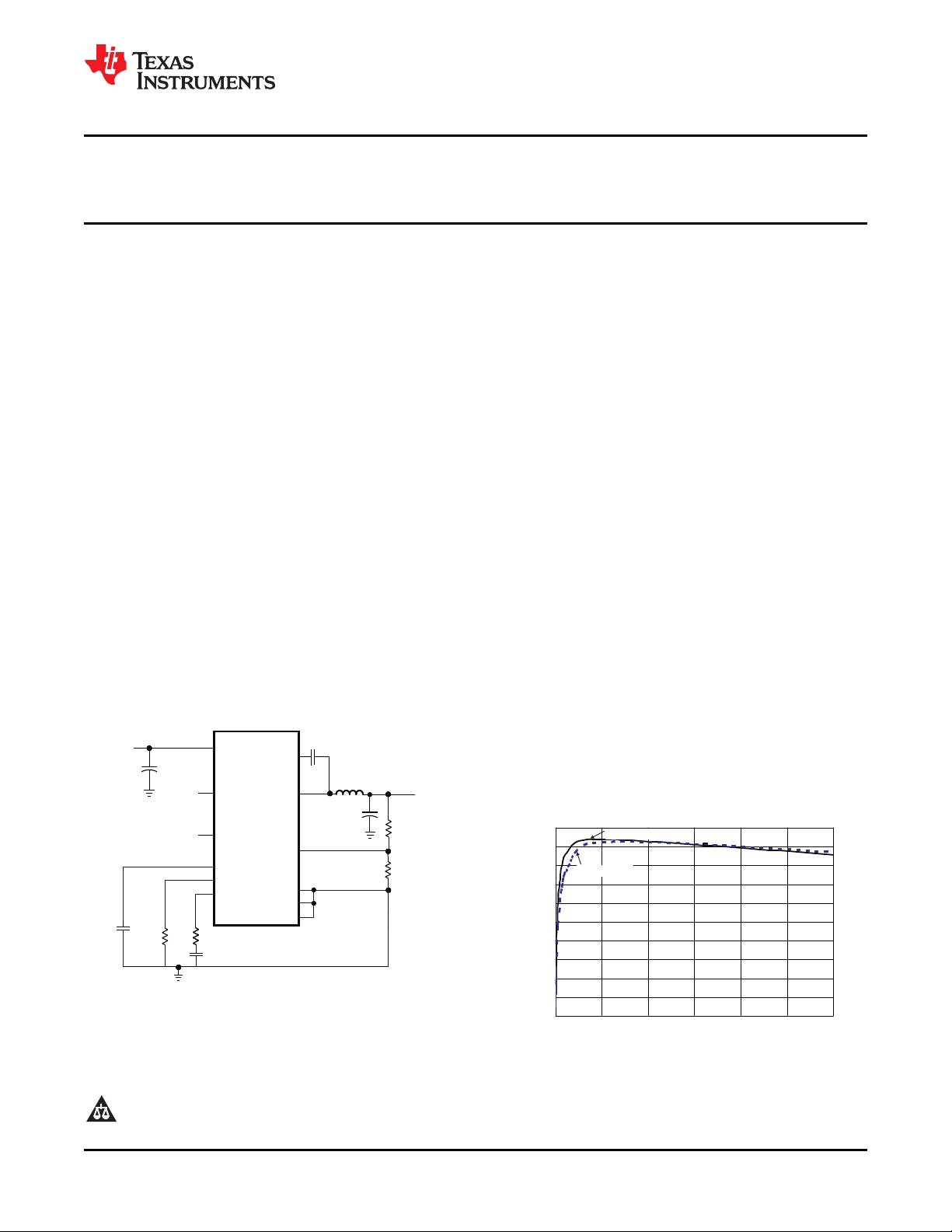
2.95-V to 6-V Input, 3-A Output, 2-MHz, Synchronous Step-Down
Switcher With Integrated FETs ( SWIFT™)
Check for Samples: TPS54319
1
FEATURES
2
• Two 45-mΩ (typical) MOSFETs for High
Efficiency at 3-A Loads
• 300kHz to 2MHz Switching Frequency
• 0.8 V ± 3.0% Voltage Reference Over
Temperature (0°C to 85°C)
• Synchronizes to External Clock
• Adjustable Slow Start/Sequencing
• UV and OV Power Good Output
• –40°C to 150°C Operating Junction
Temperature Range
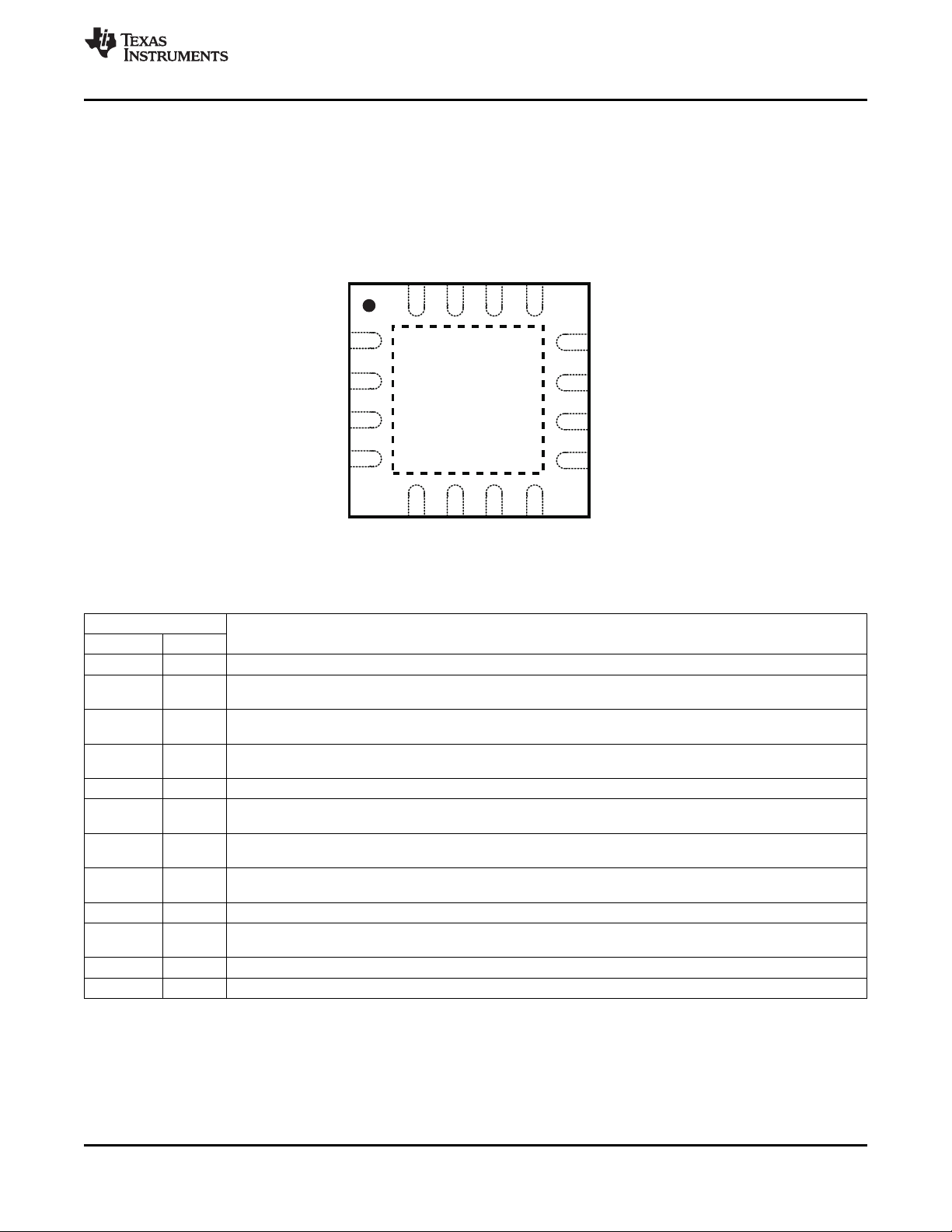
• Thermally Enhanced 3mm × 3mm 16-pin QFN
• Pin Compatible to TPS54318
APPLICATIONS
• Low-Voltage, High-Density Power Systems
• Point-of-Load Regulation for Consumer
Applications such as Set Top Boxes, LCD
Displays, CPE Equipment
SIMPLIFIED SCHEMATIC
vertical spacer
vertical spacer
SLVSA83 –JUNE 2010
DESCRIPTION
The TPS54319 device is a full featured 6 V, 3 A,
synchronous step down current mode converter with
two integrated MOSFETs.
The TPS54319 enables small designs by integrating
the MOSFETs, implementing current mode control to
reduce external component count, reducing inductor
size by enabling up to 2 MHz switching frequency,
and minimizing the IC footprint with a small 3mm x
3mm thermally enhanced QFN package.
The TPS54319 provides accurate regulation for a
variety of loads with an accurate ±3.0% Voltage
Reference (VREF) over temperature.
Efficiency is maximized through the integrated 45mΩ
MOSFETs and 360mA typical supply current. Using
the enable pin, shutdown supply current is reduced to
2 µA by entering a shutdown mode.
Under voltage lockout is internally set at 2.6 V, but
can be increased by programming the threshold with
a resistor network on the enable pin. The output
voltage startup ramp is controlled by the slow start
pin. An open drain power good signal indicates the
output is within 93% to 107% of its nominal voltage.
Frequency fold back and thermal shutdown protects
the device during an over-current condition.
The TPS54319 is supported in the SwitcherPro™
Software Tool at www.ti.com/switcherpro.
For more SWIFTTMdocumentation, see the TI
website at www.ti.com/swift.
1
2SWIFT, SwitcherPro are trademarks of Texas Instruments.
PRODUCTION DATA information is current as of publication date.
Products conform to specifications per the terms of the Texas
Instruments standard warranty. Production processing does not
necessarily include testing of all parameters.
Please be aware that an important notice concerning availability, standard warranty, and use in critical applications of Texas
Instruments semiconductor products and disclaimers thereto appears at the end of this data sheet.
Copyright © 2010, Texas Instruments Incorporated
Page 2
TPS54319
SLVSA83 –JUNE 2010
www.ti.com
These devices have limited built-in ESD protection. The leads should be shorted together or the device placed in conductive foam
during storage or handling to prevent electrostatic damage to the MOS gates.
ORDERING INFORMATION
T
J
PACKAGE PART NUMBER
(1)
–40°C to 150°C 3 × 3 mm QFN TPS54319RTE
(1) For the most current package and ordering information, see the Package Option Addendum at the end
of this document, or see the TI website at www.ti.com
ABSOLUTE MAXIMUM RATINGS
(1)
VALUE UNIT
MIN MAX
Input voltage VIN –0.3 7
EN –0.3 7
BOOT PH + 7
VSENSE –0.3 3
COMP –0.3 3
V
PWRGD –0.3 7
SS/TR –0.3 3
RT/CLK –0.3 6
Output voltage BOOT-PH 7
PH –0.6 7 V
PH 10 ns Transient –2 10
Source current EN 100 µA
RT/CLK 100 µA
Sink current COMP 100 µA
PWRGD 10 mA
SS/TR 100 µA
Electrostatic discharge (HBM) QSS 009-105 (JESD22-A114A)
(2)
1 kV
Electrostatic discharge (CDM) QSS 009-147 (JESD22-C101B.01) 500 V
Temperature T
j
T
stg
–40 150 °C
–65 150 °C
(1) Stresses beyond those listed under absolute maximum ratings may cause permanent damage to the device. These are stress ratings
only, and functional operation of the device at these or any other conditions beyond those indicated under ELECTRICAL
SPECIFICATIONS is not implied. Exposure to absolute-maximum-rated conditions for extended periods may affect device reliability.
(2) The human body model is a 100-pF capacitor discharged through a 1.5-kΩ resistor into each pin. The machine model is a 200-pF
capacitor discharged directly into each pin.
2 Submit Documentation Feedback Copyright © 2010, Texas Instruments Incorporated
Product Folder Link(s): TPS54319
Page 3
TPS54319
www.ti.com
SLVSA83 –JUNE 2010
THERMAL INFORMATION
(1)(2)
(3)
q
JA
q
JA
y
JT
y
JB
q
JC(top)
q
JC(bottom)
q
JB
THERMAL METRIC
Junction-to-ambient thermal resistance (standard board) 51.7
Junction-to-ambient thermal resistance (custom board)
Junction-to-top characterization parameter 0.8
Junction-to-board characterization parameter 19.2 °C/W
Junction-to-case(top) thermal resistance 69.3
Junction-to-case(bottom) thermal resistance 6.2
Junction-to-board thermal resistance 22
(1) For more information about traditional and new thermal metrics, see the IC Package Thermal Metrics application report, SPRA953.
(2) Power rating at a specific ambient temperature TAshould be determined with a junction temperature of 150°C. This is the point where
distortion starts to substantially increase. See power dissipation estimate in application section of this data sheet for more information.
(3) Test boards conditions:
(a) 2 inches x 2 inches, 4 layers, thickness: 0.062 inch
(b) 2 oz. copper traces located on the top of the PCB
(c) 2 oz. copper ground planes on the 2 internal layers and bottom layer
(d) 4 thermal vias (10mil) located under the device package
TPS54319
RTE (16-PINS)
37.0
UNITS
ELECTRICAL CHARACTERISTICS
TJ= –40°C to 150°C, VIN = 2.95 to 6 V (unless otherwise noted)
DESCRIPTION CONDITIONS MIN TYP MAX UNIT
SUPPLY VOLTAGE (VIN PIN)
Operating input voltage 2.95 6 V
Internal under voltage lockout threshold 2.6 2.8 V
Shutdown supply current EN = 0 V, 25°C, 2.95 V ≤ VIN ≤ 6 V 2 5 mA
Quiescent Current - I
q
ENABLE AND UVLO (EN PIN)
Enable threshold Rising 1.25 V
Input current mA
VOLTAGE REFERENCE (VSENSE PIN)
Voltage Reference 2.95 V ≤ VIN ≤ 6 V, 0°C <TJ< 85°C 0.802 0.827 0.852 V
MOSFET
High side switch resistance mΩ
Low side switch resistance mΩ
ERROR AMPLIFIER
Input current 7 nA
Error amplifier transconductance (gm) –2 mA < I(COMP) < 2 mA, V(COMP) = 1 V 245 mmhos
Error amplifier transconductance (gm) during –2 mA < I(COMP) < 2 mA, V(COMP) = 1 V, 79 mmhos
slow start Vsense = 0.4 V
Error amplifier source/sink V(COMP) = 1 V, 100 mV overdrive +20 mA
COMP to Iswitch gm 18 A/V
CURRENT LIMIT
Current limit threshold 3V 4.2 6.6 A
THERMAL SHUTDOWN
Thermal Shutdown 165 °C
Hysteresis 15 °C
VSENSE = 0.9 V, VIN = 5 V, 25°C, RT = 400 kΩ 360 575 mA
Falling 1.18
Enable threshold + 50 mV –4.6
Enable threshold – 50 mV –1.2
BOOT-PH= 5 V 45 81
BOOT-PH= 2.95 V 64 110
VIN= 5 V 42 81
VIN= 2.95 V 59 110
–20
Copyright © 2010, Texas Instruments Incorporated Submit Documentation Feedback 3
Product Folder Link(s): TPS54319
Page 4
TPS54319
SLVSA83 –JUNE 2010
www.ti.com
ELECTRICAL CHARACTERISTICS (continued)
TJ= –40°C to 150°C, VIN = 2.95 to 6 V (unless otherwise noted)
DESCRIPTION CONDITIONS MIN TYP MAX UNIT
TIMING RESISTOR AND EXTERNAL CLOCK (RT/CLK PIN)
Switching frequency range using RT mode 300 2000 kHz
Switching frequency Rt = 400 kΩ 400 500 600 kHz
Switching frequency range using CLK mode 300 2000 kHz
Minimum CLK pulse width 75 ns
RT/CLK voltage R(RT/CLK)= 400kΩ 0.5 V
RT/CLK high threshold 1.6 2.2 V
RT/CLK low threshold 0.4 0.6 V
RT/CLK falling edge to PH rising edge delay Measure at 500 kHz with RT resistor in series 90 ns
PLL lock in time Measure at 500 kHz 14 ms
PH (PH PIN)
Minimum On time Measured at 50% points on PH, IOUT = 3 A 65
Measured at 50% points on PH, VIN = 5 V, 120
IOUT = 0 A
Minimum Off time Prior to skipping off pulses, BOOT-PH = 2.95 V, 60 ns
Rise Time 2.5
Fall Time 2
BOOT (BOOT PIN)
BOOT Charge Resistance VIN = 5 V 16 Ω
BOOT-PH UVLO VIN = 2.95 V 2.2 V
SLOW START AND TRACKING (SS/TR PIN)
Charge Current V(SS/TR) = 0.4 V 2.2 mA
SS/TR to VSENSE matching V(SS/TR) = 0.4 V 35 mV
SS/TR to reference crossover 98% normal 1.1 V
SS/TR discharge voltage (Overload) VSENSE = 0 V 46 mV
SS/TR discharge current (Overload) VSENSE = 0 V, V(SS/TR) = 0.4 V 325 µA
POWER GOOD (PWRGD PIN)
VSENSE threshold
Hysteresis VSENSE falling 2 % Vref
Output high leakage VSENSE = VREF, V(PWRGD) = 5.5 V 2 nA
On resistance 100 200 Ω
Output low I(PWRGD) = 3.0 mA 0.3 0.6 V
Minimum VIN for valid output V(PWRGD) < 0.5 V at 100 mA 1.2 1.6 V
IOUT = 3 A
VIN = 5 V, 3 A V/ns
VSENSE falling (Fault) 91 % Vref
VSENSE rising (Good) 93 % Vref
VSENSE rising (Fault) 107 % Vref
VSENSE falling (Good) 105 % Vref
ns
4 Submit Documentation Feedback Copyright © 2010, Texas Instruments Incorporated
Product Folder Link(s): TPS54319
Page 5
PWRGD
BOOT
PH
RT/CLK
EN
AGND
VIN
VSENSE
COMP
15 14 13
GND
12
11
10
9
8
765
16
GND
VIN
VIN
PH
PH
1
2
3
4
SS/TR
PowerPAD
(17)
QFN16
RTE PACKAGE
(TOP VIEW)
TPS54319
www.ti.com
PIN CONFIGURATION
SLVSA83 –JUNE 2010
DEVICE INFORMATION
PIN FUNCTIONS
PIN
NAME NO.
AGND 5 Analog Ground should be electrically connected to GND close to the device.
BOOT 13 A bootstrap capacitor is required between BOOT and PH. If the voltage on this capacitor is below the minimum
required by the BOOT UVLO, the output is forced to switch off until the capacitor is refreshed.
COMP 7 Error amplifier output, and input to the output switch current comparator. Connect frequency compensation
components to this pin.
EN 15 Enable pin, internal pull-up current source. Pull below 1.2 V to disable. Float to enable. Can be used to set the
on/off threshold (adjust UVLO) with two additional resistors.
GND 3, 4 Power Ground. This pin should be electrically connected directly to the power pad under the IC.
PH 10, 11, The source of the internal high side power MOSFET, and drain of the internal low side (synchronous) rectifier
12 MOSFET.
PowerPAD 17 GND pin should be connected to the exposed power pad for proper operation. This power pad should be
PWRGD 14 An open drain output; asserts low if output voltage is low due to thermal shutdown, overcurrent,
connected to any internal PCB ground plane using multiple vias for good thermal performance.
over/under-voltage or EN shut down.
RT/CLK 8 Resistor Timing or External Clock input pin.
SS/TR 9 Slow start and tracking. An external capacitor connected to this pin sets the output voltage rise time.
This pin can also be used for tracking.
VIN 1, 2, 16 Input supply voltage, 2.95 V to 6 V.
VSENSE 6 Inverting node of the transconductance (gm) error amplifier.
DESCRIPTION
Copyright © 2010, Texas Instruments Incorporated Submit Documentation Feedback 5
Product Folder Link(s): TPS54319
Page 6
ERROR
AMPLIFIER
Boot
Charge
Boot
UVLO
UVLO
Current
Sense
Oscillator
with PLL
Frequency
Shift
Slope
Compensation
PWM
Comparator
Minimum
COMP Clamp
Maximum
Clamp
Voltage
Reference
Overload
Recovery
VSENSE
SS/TR
COMP
RT/CLK
PH
BOOT
VIN
AGND
Thermal
Shutdown
EN
Enable
Comparator
Shutdown
Logic
Shutdown
Enable
Threshold
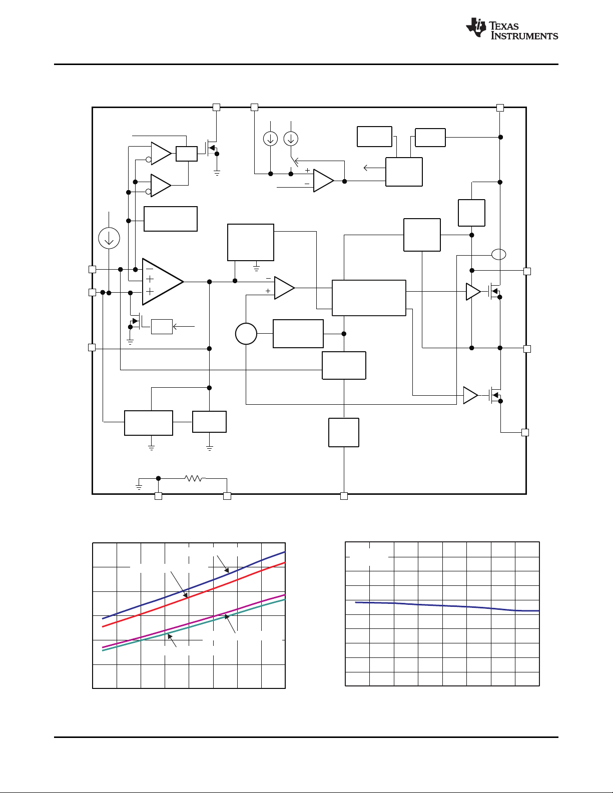
TPS54319RTE Block Diagram
Logic
Shutdown
PWRGD
POWERPAD
GND
Logic
Shutdown
107%
93%
S
Logic and PWM
Latch
i
1
i
hys
RT =400k ,
V =5V
W
I
-50 -25 0 25 50 75 100 125 150
T -JunctionTemperature-°C
J
450
455
460
465
470
475
480
485
490
495
500
f -SwitchingFrequency-kHz
s
0.02
0.03
0.04
0.05
0.06
0.07
0.08
RDSON - Static Drain-Source On-State Resistance - W
-50 -25 0 25 50 75 100 125 150
T - Junction Temperature - °C
J
High Side Rdson V = 3.3 V
IN
Low Side Rdson V = 3.3 V
IN
Low Side Rdson V = 5 V
IN
High Side Rdson V = 5 V
IN
TPS54319
SLVSA83 –JUNE 2010
FUNCTIONAL BLOCK DIAGRAM
www.ti.com
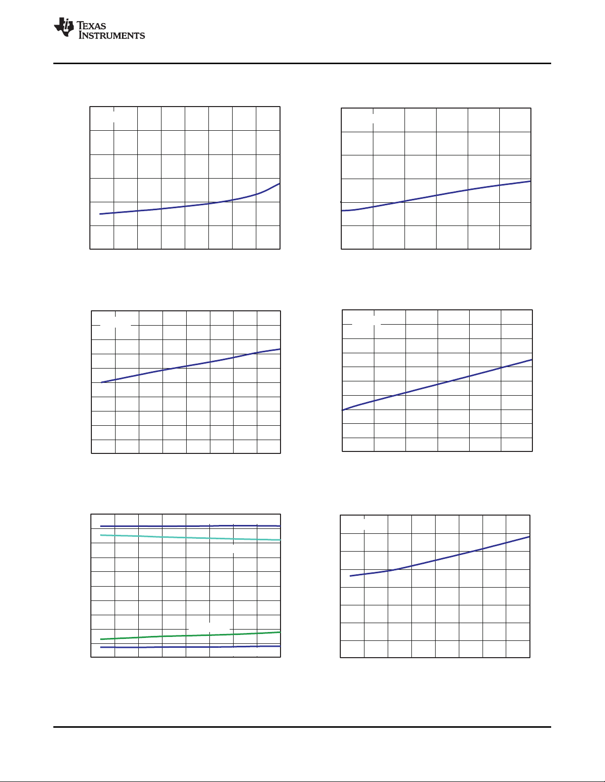
HIGH SIDE AND LOW SIDE Rdson vs TEMPERATURE FREQUENCY vs TEMPERATURE
6 Submit Documentation Feedback Copyright © 2010, Texas Instruments Incorporated
Figure 1. Figure 2.
TYPICAL CHARACTERISTICS CURVES
Product Folder Link(s): TPS54319
Page 7
0.798
0.808
0.818
0.828
0.838
0.848
V =3.3V
I
0.858
-50 -25 0 25 50 75 100 125 150
T -JunctionTemperature-°C
J
V -VoltageReference-V
ref
V =3V
I
V =5V
I
-50 -25 0 25 50 75 100 125 150
T -JunctionTemperature-°C
J
6
6.2
6.4
6.6
6.8
7
7.2
7.4
7.6
7.8
8
HighSideSwitchCurrent- A
1000
1100
1200
1300
1400
1500
1600
1700
1800
1900
2000
80 100 120 140 160 180 200
RT-ResistancekW
f -SwitchingFrequency-KHz
s
300 400 500 600 700 800 900
1000
RT - Resistance - kW
200
300
400
500
600
700
800
900
1000
f - Switching Frequncy - KHz
s
0
25
50
75
100
0 0.1 0.2 0.3 0.4 0.5 0.6 0.7 0.8
Vsense-V
VsenseFalling
VsenseRising
NominalSwitchingFrequency-%
170
190
210
230
250
270
290
310
-50 -25 0 25 50 75 100 125 150
T -JunctionTemperature-°C
J
EA -Transconductance- A/Vm
V =3.3V
I
TPS54319
www.ti.com
SLVSA83 –JUNE 2010
TYPICAL CHARACTERISTICS CURVES (continued)
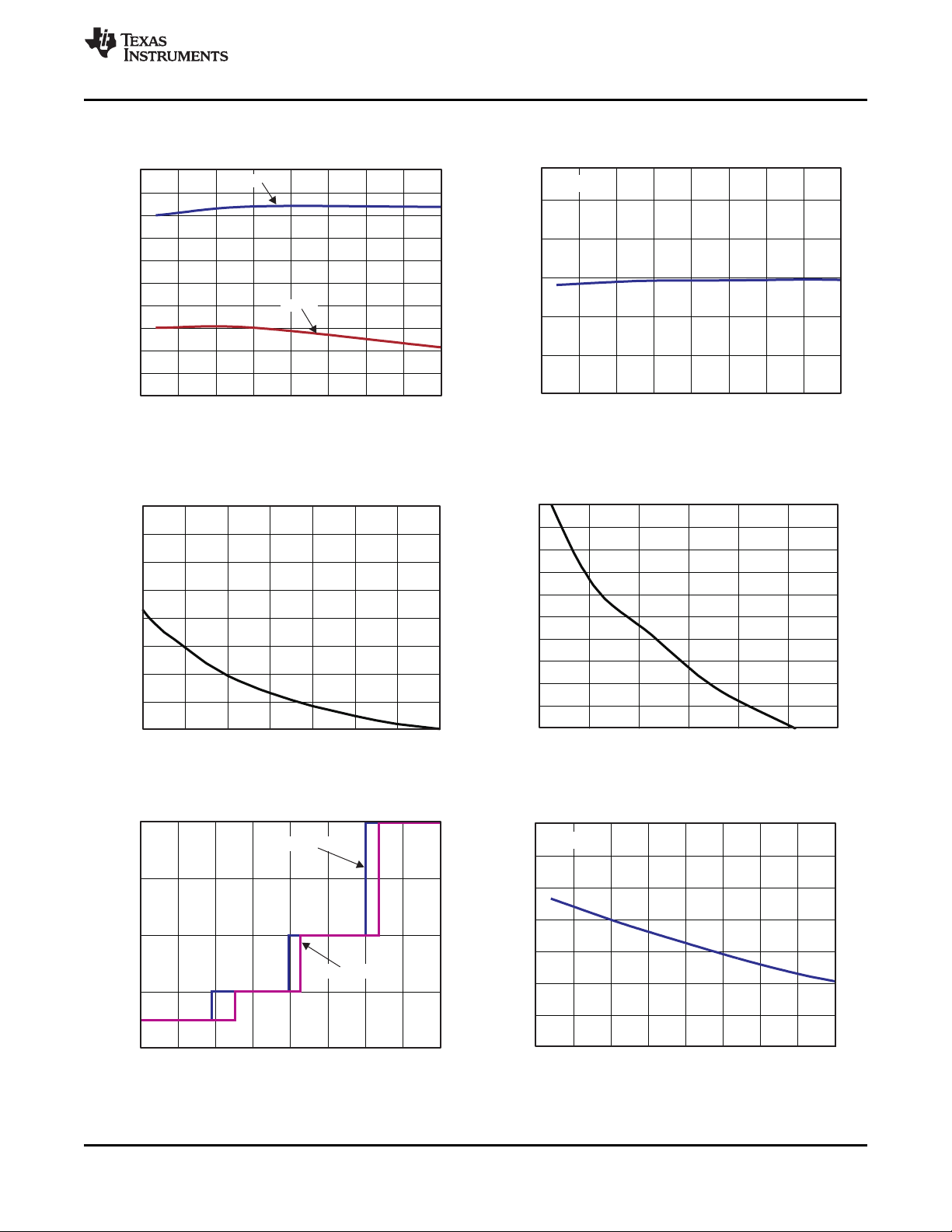
HIGH SIDE CURRENT LIMIT vs TEMPERATURE VOLTAGE REFERENCE vs TEMPERATURE
Figure 3. Figure 4.
SWITCHING FREQUENCY vs SWITCHING FREQUENCY vs
RT RESISTANCE LOW FREQUENCY RANGE RT RESISTANCE HIGH FREQUENCY RANGE
Figure 5. Figure 6.
SWITCHING FREQUENCY vs VSENSE TRANSCONDUCTANCE vs TEMPERATURE
Copyright © 2010, Texas Instruments Incorporated Submit Documentation Feedback 7
Figure 7. Figure 8.
Product Folder Link(s): TPS54319
Page 8
55
60
65
70
75
80
85
90
95
100
105
V =3.3V
I
-50 -25 0 25 50 75 100 125 150
T -JunctionTemperature-°C
J
EA -Transconductance- A/Vm
1.15
1.16
1.17
1.18
1.19
1.2
1.21
1.22
1.23
1.24
1.25
1.26
1.27
1.28
1.29
1.3
V =3.3V,rising
I
-50 -25 0 25 50 75 100 125 150
T -JunctionTemperature-°C
J
V =3.3V,falling
I
EN-Threshold-V
-5.15
-5.05
-4.95
-4.85
-4.75
-4.65
-4.55
-4.45
-4.35
-4.25
V = 5 V,
Ven = Threshold +50 mV
I
-50 -25 0 25 50 75 100 125 150
T - Junction Temperature - °C
J
EN - Pin Current - Am
-1.65
-1.55
-1.45
-1.35
-1.25
-1.15
-1.05
-0.95
-0.85
V = 5 V,
Ven = Threshold -50 mV
I
EN - Pin Current - Am
-50 -25 0 25 50 75 100 125 150
T - Junction Temperature - °C
J
-3
-2.8
-2.6
-2.4
-2.2
-2
-1.8
-1.6
-1.4
-50 -30 -10 10 30 50 70 90 110 130 150
T - Junction Temperature - °C
J
V = 5 V
I
Iss/tr - Charge Current - Am
2.2
2.3
2.4
2.5
2.6
2.7
2.8
2.9
3
UVLOStartSwitching
UVLOStopSwitching
-50 -25 0 25 50 75 100 125 150
T -JunctionTemperature-°C
J
V -InputVoltage-V
I
TPS54319
SLVSA83 –JUNE 2010
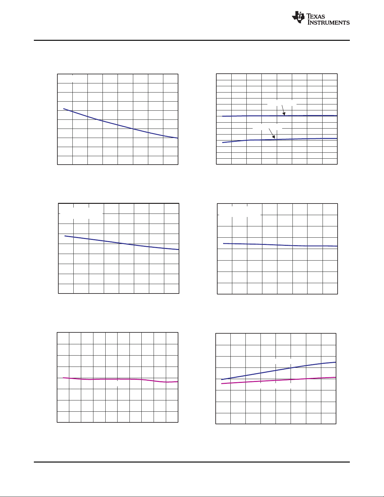
TRANSCONDUCTANCE (SLOW START) vs
EN PIN CURRENT vs TEMPERATURE EN PIN CURRENT vs TEMPERATURE
www.ti.com
TYPICAL CHARACTERISTICS CURVES (continued)
JUNCTION TEMPERATURE EN PIN VOLTAGE vs TEMPERATURE
Figure 9. Figure 10.
Figure 11. Figure 12.
CHARGE CURRENT vs TEMPERATURE INPUT VOLTAGE vs TEMPERATURE
8 Submit Documentation Feedback Copyright © 2010, Texas Instruments Incorporated
Figure 13. Figure 14.
Product Folder Link(s): TPS54319
Page 9
0
0.5
1
1.5
2
2.5
3
ShutdownSupplyCurrent- Am
V =3.3V
I
-50 -25 0 25 50 75 100 125 150
T -JunctionTemperature-°C
J
3 3.5 4 4.5 5 5.5 6
V -InputVoltage-V
I
T =25°C
J
0
0.5
1
1.5
2
2.5
3
ShutdownSupplyCurrent- Am
325
335
345
355
365
375
385
395
405
415
425
3 3.5 4 4.5 5 5.5 6
V -InputVoltage-V
I
Ivin-SupplyCurrent- Am
T =25°C
J
300
310
320
330
340
350
360
370
380
390
400
-50 -25 0 25 50 75 100 125 150
T -JunctionTemperature-°C
J
Ivin-SupplyCurrent- Am
V =3.3V
I
90
92
94
96
98
100
102
104
106
108
110
VsenseRising,V =5V
I
VsenseRising
VsenseFalling
-50 -25 0 25 50 75 100 125 150
T -JunctionTemperature-°C
J
PWRGDThreshold-%Vref
VsenseFalling
0
20
40
60
80
100
120
140
160
-50 -25 0 25 50 75 100 125 150
T -JunctionTemperature-°C
J
V =3.3V
I
RDSON-StaticDrain-SourceOn-StateResistance- W
TPS54319
www.ti.com
SLVSA83 –JUNE 2010
TYPICAL CHARACTERISTICS CURVES (continued)
SHUTDOWN SUPPLY CURRENT vs TEMPERATURE SHUTDOWN SUPPLY CURRENT vs INPUT VOLTAGE
Figure 15. Figure 16.
VIN SUPPLY CURRENT vs JUNCTION TEMPERATURE VIN SUPPLY CURRENT vs INPUT VOLTAGE
Figure 17. Figure 18.
PWRGD THRESHOLD vs TEMPERATURE PWRGD ON-RESISTANCE vs TEMPERATURE
Copyright © 2010, Texas Instruments Incorporated Submit Documentation Feedback 9
Figure 19. Figure 20.
Product Folder Link(s): TPS54319
Page 10
0
10
20
30
40
50
60
70
V =5V,
SS=0.3V
I
80
-50 -25 0 25 50 75 100 125 150
T -JunctionTemperature-°C
J
SS/TR-VsenseOffset-mV
TPS54319
SLVSA83 –JUNE 2010
TYPICAL CHARACTERISTICS CURVES (continued)
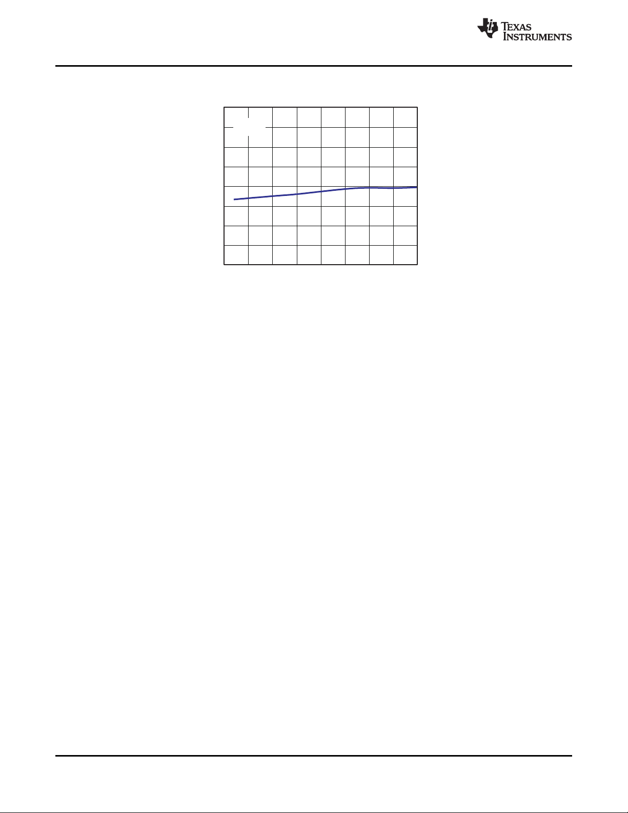
SS/TR to VSENSE OFFSET vs TEMPERATURE
Figure 21.
OVERVIEW
The TPS54319 is a 6-V, 3-A, synchronous step-down (buck) converter with two integrated n-channel MOSFETs.
To improve performance during line and load transients the device implements a constant frequency, peak
current mode control which reduces output capacitance and simplifies external frequency compensation design.
The wide switching frequency of 300 kHz to 2000 kHz allows for efficiency and size optimization when selecting
the output filter components. The switching frequency is adjusted using a resistor to ground on the RT/CLK pin.
The device has an internal phase lock loop (PLL) on the RT/CLK pin that is used to synchronize the power
switch turn on to a falling edge of an external system clock.
The TPS54319 has a typical default start up voltage of 2.6 V. The EN pin has an internal pull-up current source
that can be used to adjust the input voltage under voltage lockout (UVLO) with two external resistors. In addition,
the pull up current provides a default condition when the EN pin is floating for the device to operate. The total
operating current for the TPS54319 is typically 360 mA when not switching and under no load. When the device
is disabled, the supply current is less than 5 mA.
The integrated 45 mΩ MOSFETs allow for high efficiency power supply designs with continuous output currents
up to 3 amperes.
The TPS54319 reduces the external component count by integrating the boot recharge diode. The bias voltage
for the integrated high side MOSFET is supplied by a capacitor between the BOOT and PH pins. The boot
capacitor voltage is monitored by an UVLO circuit and turns off the high side MOSFET when the voltage falls
below a preset threshold. This BOOT circuit allows the TPS54319 to operate approaching 100%. The output
voltage can be stepped down to as low as the 0.827 V reference.
The TPS54319 has a power good comparator (PWRGD) with 2% hysteresis.
The TPS54319 minimizes excessive output over-voltage transients by taking advantage of the over-voltage
power good comparator. When the regulated output voltage is greater than 107% of the nominal voltage, the
over-voltage comparator is activated, and the high side MOSFET is turned off and masked from turning on until
the output voltage is lower than 105%.
The SS/TR (slow start/tracking) pin is used to minimize inrush currents or provide power supply sequencing
during power up. A small value capacitor should be coupled to the pin for slow start. The SS/TR pin is
discharged before the output power up to ensure a repeatable restart after an over-temperature fault, UVLO fault
or disabled condition.
The use of a frequency fold-back circuit reduces the switching frequency during startup and over current fault
conditions to help limit the inductor current.
www.ti.com
10 Submit Documentation Feedback Copyright © 2010, Texas Instruments Incorporated
Product Folder Link(s): TPS54319
Page 11

O
0.827 V
R2 = R1
V 0.827 V
æ ö
´
ç ÷
-
è ø
TPS54319
www.ti.com
SLVSA83 –JUNE 2010
DETAILED DESCRIPTION
FIXED FREQUENCY PWM CONTROL
The TPS54319 uses an adjustable fixed frequency, peak current mode control. The output voltage is compared
through external resistors on the VSENSE pin to an internal voltage reference by an error amplifier which drives
the COMP pin. An internal oscillator initiates the turn on of the high side power switch. The error amplifier output
is compared to the high side power switch current. When the power switch current reaches the COMP voltage
level the high side power switch is turned off and the low side power switch is turned on. The COMP pin voltage
increases and decreases as the output current increases and decreases. The device implements a current limit
by clamping the COMP pin voltage to a maximum level and also implements a minimum clamp for improved
transient response performance.
SLOPE COMPENSATION AND OUTPUT CURRENT
The TPS54319 adds a compensating ramp to the switch current signal. This slope compensation prevents
sub-harmonic oscillations as duty cycle increases. The available peak inductor current remains constant over the
full duty cycle range.
BOOTSTRAP VOLTAGE (BOOT) AND LOW DROPOUT OPERATION
The TPS54319 has an integrated boot regulator and requires a small ceramic capacitor between the BOOT and
PH pin to provide the gate drive voltage for the high side MOSFET. The value of the ceramic capacitor should be
0.1 mF. A ceramic capacitor with an X7R or X5R grade dielectric with a voltage rating of 10 V or higher is
recommended because of the stable characteristics over temperature and voltage.
To improve drop out, the TPS54319 is designed to operate at 100% duty cycle as long as the BOOT to PH pin
voltage is greater than 2.2 V. The high side MOSFET is turned off using an UVLO circuit, allowing for the low
side MOSFET to conduct when the voltage from BOOT to PH drops below 2.2 V. Since the supply current
sourced from the BOOT pin is very low, the high side MOSFET can remain on for more switching cycles than are
required to refresh the capacitor, thus the effective duty cycle of the switching regulator is very high.
ERROR AMPLIFIER
The TPS54319 has a transconductance amplifier. The error amplifier compares the VSENSE voltage to the lower
of the SS/TR pin voltage or the internal 0.827 V voltage reference. The transconductance of the error amplifier is
245mA/V during normal operation. When the voltage of VSENSE pin is below 0.827 V and the device is
regulating using the SS/TR voltage, the gm is typically greater than 79 mA/V, but less than 245 mA/V. The
frequency compensation components are placed between the COMP pin and ground.
VOLTAGE REFERENCE
The voltage reference system produces a precise ±3.0% voltage reference over temperature by scaling the
output of a temperature-stable bandgap circuit. The bandgap and scaling circuits produce 0.827 V at the
non-inverting input of the error amplifier.
ADJUSTING THE OUTPUT VOLTAGE
The output voltage is set with a resistor divider from the output node to the VSENSE pin. It is recommended to
use divider resistors with 1% tolerance or better. Start with a 100 kΩ for the R1 resistor and use the Equation 1
to calculate R2. To improve efficiency at very light loads consider using larger value resistors. If the values are
too high the regulator is more susceptible to noise and voltage errors from the VSENSE input current are
noticeable.
vertical spacer
vertical spacer
(1)
Copyright © 2010, Texas Instruments Incorporated Submit Documentation Feedback 11
Product Folder Link(s): TPS54319
Page 12
VSENSE
V
O
+
–
TPS54319
R1
R2
0.827 V
EN
i
1
i
hys
VIN
+
–
TPS54319
R1
R2
1.2 mA
3.4 mA
( )
START STOP
6
0.944 V V
R1 =
3.47 10
-
´ -
W
´
( )
6
STOP
1.18 R1
R2 =
V 1.18 4.6 10 R1
-
×
W
- + ´ ×
Tss(mS) Iss( A)
Css(nF) =
Vref(V)
´ m
TPS54319
SLVSA83 –JUNE 2010
www.ti.com
Figure 22. Voltage Divider Circuit
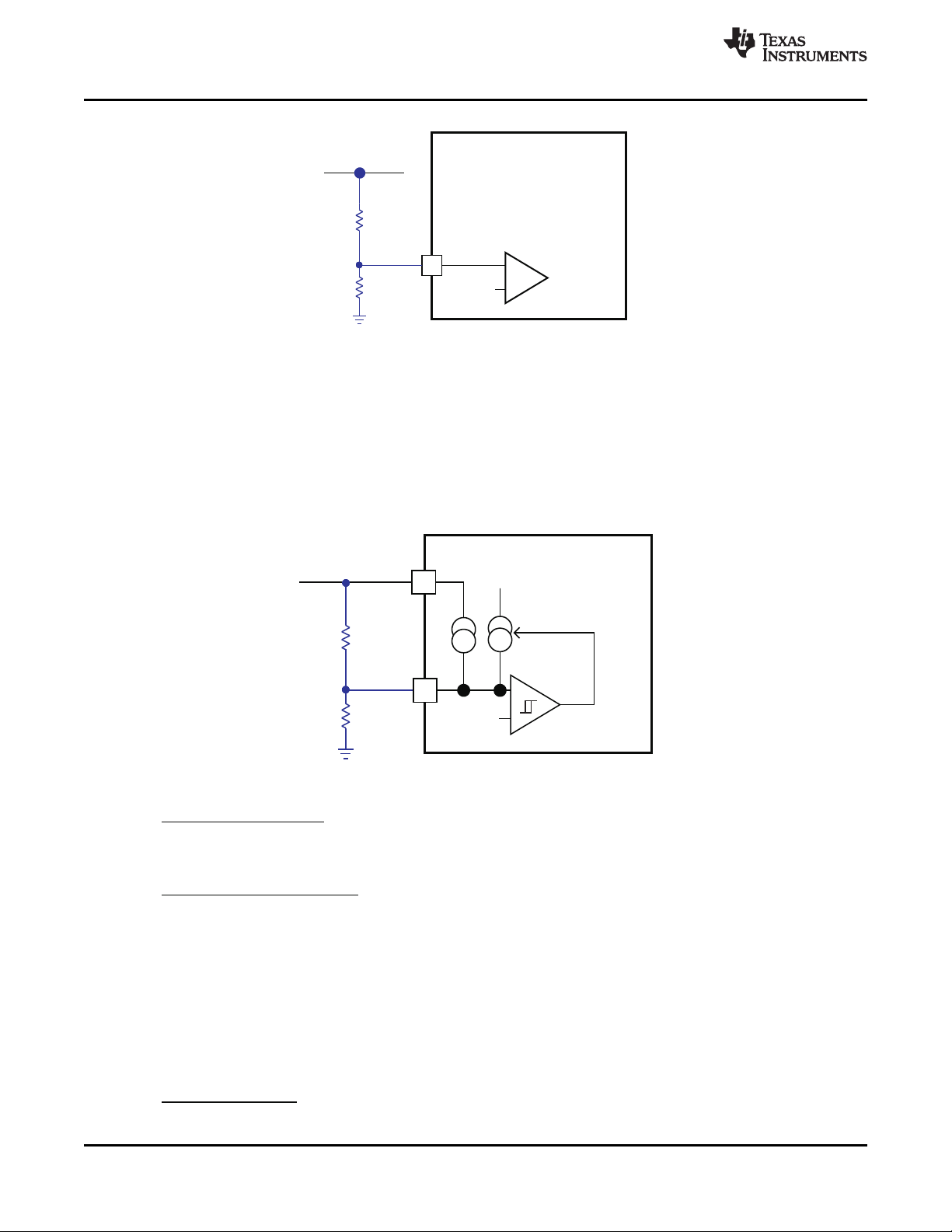
ENABLE AND ADJUSTING UNDER-VOLTAGE LOCKOUT
The TPS54319 is disabled when the VIN pin voltage falls below 2.6 V. If an application requires a higher
under-voltage lockout (UVLO), use the EN pin as shown in Figure 23 to adjust the input voltage UVLO by using
two external resistors. The EN pin has an internal pull-up current source that provides the default condition of the
TPS54319 operating when the EN pin floats. Once the EN pin voltage exceeds 1.25 V, an additional 3.4 mA of
hysteresis is added. When the EN pin is pulled below 1.18 V, the 3.4 mA is removed. This additional current
facilitates input voltage hysteresis.
vertical spacer
SLOW START / TRACKING PIN
The TPS54319 regulates to the lower of the SS/TR pin and the internal reference voltage. A capacitor on the
SS/TR pin to ground implements a slow start time. The TPS54319 has an internal pull-up current source of
2.2mA which charges the external slow start capacitor. Equation 4 calculates the required slow start capacitor
value where Tss is the desired slow start time in ms, Iss is the internal slow start charging current of 2.2 mA, and
Vref is the internal voltage reference of 0.827 V.
vertical spacer
12 Submit Documentation Feedback Copyright © 2010, Texas Instruments Incorporated
Figure 23. Adjustable Under Voltage Lock Out
(2)
(3)
(4)
Product Folder Link(s): TPS54319
Page 13

SS2
TPS54319
EN2
PWRGD2
SS1
EN1
PWRGD1
Vo ut 2
Vo ut 1
P WR GD 1
E N2
EN1
TPS54319
www.ti.com
SLVSA83 –JUNE 2010
If during normal operation, the VIN goes below the UVLO, EN pin pulled below 1.2 V, or a thermal shutdown
event occurs, the TPS54319 stops switching. When the VIN goes above UVLO, EN is released or pulled high, or
a thermal shutdown is exited, then SS/TR is discharged to below 40 mV before reinitiating a powering up
sequence. The VSENSE voltage will follow the SS/TR pin voltage with a 35mV offset up to 85% of the internal
voltage reference. When the SS/TR voltage is greater than 85% on the internal reference voltage the offset
increases as the effective system reference transitions from the SS/TR voltage to the internal voltage reference.
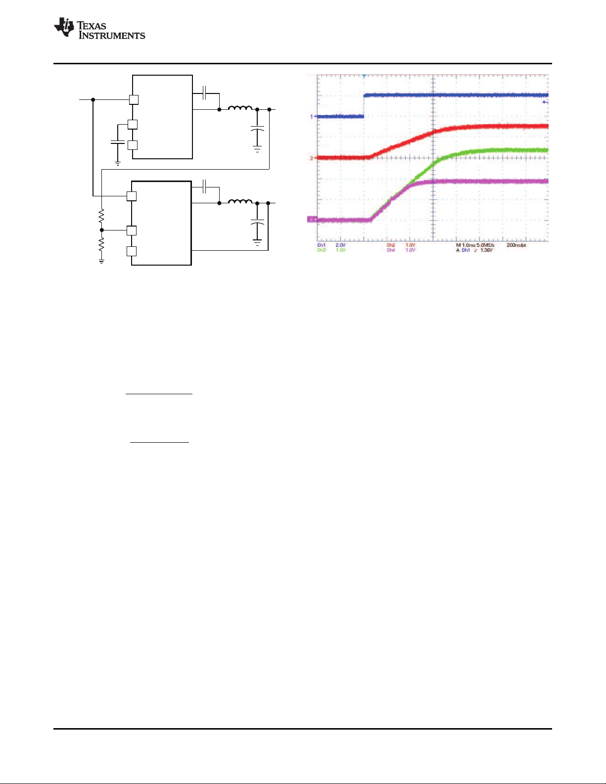
SEQUENCING
Many of the common power supply sequencing methods can be implemented using the SS/TR, EN and PWRGD
pins. The sequential method can be implemented using an open drain or collector output of a power on reset pin
of another device. Figure 24 shows the sequential method. The power good is coupled to the EN pin on the
TPS54319 which enables the second power supply once the primary supply reaches regulation.
Ratio-metric start up can be accomplished by connecting the SS/TR pins together. The regulator outputs ramp
up and reach regulation at the same time. When calculating the slow start time the pull up current source must
be doubled in Equation 4. The ratio metric method is illustrated in Figure 26.
Figure 24. Sequential Start-Up Sequence Figure 25. Sequential Startup using EN and
PWRGD
Copyright © 2010, Texas Instruments Incorporated Submit Documentation Feedback 13
Product Folder Link(s): TPS54319
Page 14

SS1
Vo ut 2
E N1 /2
Vo ut 1
SS/TR1
TPS54319
EN1
PWRGD1
SS/TR2
TPS54319
EN2
PWRGD2
D
´
Vo ut2 + V Vssoffse t
R1 =
Vref Iss
´
D -
Vref R1
R2 =
Vout2 + V Vref
V = Vout1 Vout2D -
R1 2930 Vout1 145 V> ´ - ´ D
TPS54319
SLVSA83 –JUNE 2010
www.ti.com
Figure 26. Schematic for Ratio-metric Start-Up Figure 27. Ratio-metric Startup with Vout1 Leading
Sequence Vout2
vertical spacer
Ratio-metric and simultaneous power supply sequencing can be implemented by connecting the resistor network
of R1 and R2 shown in Figure 28 to the output of the power supply that needs to be tracked or another voltage
reference source. Using Equation 5 and Equation 6, the tracking resistors can be calculated to initiate the Vout2
slightly before, after or at the same time as Vout1. Equation 7 is the voltage difference between Vout1 and
Vout2. The ΔV variable is zero volts for simultaneous sequencing. To minimize the effect of the inherent SS/TR
to VSENSE offset (Vssoffset) in the slow start circuit and the offset created by the pullup current source (Iss) and
tracking resistors, the Vssoffset and Iss are included as variables in the equations. To design a ratio-metric start
up in which the Vout2 voltage is slightly greater than the Vout1 voltage when Vout2 reaches regulation, use a
negative number in Equation 5 through Equation 7 for ΔV. Equation 7 will result in a positive number for
applications which the Vout2 is slightly lower than Vout1 when Vout2 regulation is achieved. Since the SS/TR pin
must be pulled below 40mV before starting after an EN, UVLO or thermal shutdown fault, careful selection of the
tracking resistors is needed to ensure the device will restart after a fault. Make sure the calculated R1 value from
Equation 5 is greater than the value calculated in Equation 8 to ensure the device can recover from a fault. As
the SS/TR voltage becomes more than 85% of the nominal reference voltage the Vssoffset becomes larger as
the slow start circuits gradually handoff the regulation reference to the internal voltage reference. The SS/TR pin
voltage needs to be greater than 1.1 V for a complete handoff to the internal voltage reference as shown in
Figure 27.
vertical spacer
vertical spacer
vertical spacer
vertical spacer
vertical spacer
14 Submit Documentation Feedback Copyright © 2010, Texas Instruments Incorporated
(5)
(6)
(7)
(8)
Product Folder Link(s): TPS54319
Page 15
EN1
Vout2
SS2
Vout1
SS/TR1
TPS54319
EN1
PWRGD1
SS/TR2
TPS54319
EN2
PWRGD2
VOUT1
VOUT 2
R1
R2
W
1.0793
311890
RT (k ) =
Fsw(kHz)
0.9393
133870
Fsw(kHz)
RT(k )=W
TPS54319
www.ti.com
SLVSA83 –JUNE 2010
Figure 28. Ratio-metric and Simultaneous Startup Figure 29. Ratio-metric Start-Up using Coupled
Sequence SS/TR Pins
CONSTANT SWITCHING FREQUENCY and TIMING RESISTOR (RT/CLK Pin)
The switching frequency of the TPS54319 is adjustable over a wide range from 300 kHz to 2000 kHz by placing
a maximum of 700 kΩ and minimum of 85 kΩ, respectively, on the RT/CLK pin. An internal amplifier holds this
pin at a fixed voltage when using an external resistor to ground to set the switching frequency. The RT/CLK is
typically 0.5 V. To determine the timing resistance for a given switching frequency, use the curve in Figure 5 and
Figure 6, or Equation 9.
vertical spacer
To reduce the solution size one would typically set the switching frequency as high as possible, but tradeoffs of
the efficiency, maximum input voltage and minimum controllable on time should be considered.
The minimum controllable on time is typically 65 ns at full current load and 120 ns at no load, and limits the
maximum operating input voltage or output voltage.
OVERCURRENT PROTECTION
The TPS54319 implements a cycle by cycle current limit. During each switching cycle the high side switch
current is compared to the voltage on the COMP pin. When the instantaneous switch current intersects the
COMP voltage, the high side switch is turned off. During overcurrent conditions that pull the output voltage low,
the error amplifier responds by driving the COMP pin high, increasing the switch current. The error amplifier
output is clamped internally. This clamp functions as a switch current limit.
FREQUENCY SHIFT
To operate at high switching frequencies and provide protection during overcurrent conditions, the TPS54319
implements a frequency shift. If frequency shift was not implemented, during an overcurrent condition the low
side MOSFET may not be turned off long enough to reduce the current in the inductor, causing a current
runaway. With frequency shift, during an overcurrent condition the switching frequency is reduced from 100%,
then 50%, then 25%, then 12.5% as the voltage decreases from 0.827 to 0 volts on VSENSE pin to allow the low
side MOSFET to be off long enough to decrease the current in the inductor. During start-up, the switching
frequency increases as the voltage on VSENSE increases from 0 to 0.827 volts. See Figure 7 for details.
Copyright © 2010, Texas Instruments Incorporated Submit Documentation Feedback 15
Product Folder Link(s): TPS54319
(9)
(10)
Page 16
TPS54319
Clock
Source
PLL
R
T
RT/CLK
SYNCClock=2V/div
PH=2V/div
Time=500nsec/div
TPS54319
SLVSA83 –JUNE 2010
www.ti.com
REVERSE OVERCURRENT PROTECTION
The TPS54319 implements low side current protection by detecting the voltage across the low side MOSFET.
When the converter sinks current through its low side FET, the control circuit turns off the low side MOSFET if
the reverse current is typically more than 2 A. By implementing this additional protection scheme, the converter is
able to protect itself from excessive current during power cycling and start-up into pre-biased outputs.
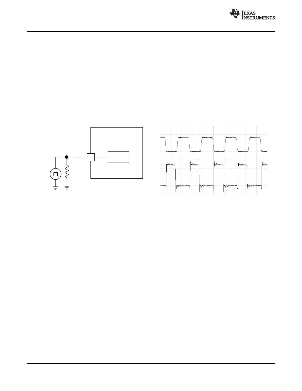
SYNCHRONIZE USING THE RT/CLK PIN
The RT/CLK pin is used to synchronize the converter to an external system clock. See Figure 30. To implement
the synchronization feature in a system, connect a square wave to the RT/CLK pin with an on time of at least
75ns. If the pin is pulled above the PLL upper threshold, a mode change occurs and the pin becomes a
synchronization input. The internal amplifier is disabled and the pin is a high impedance clock input to the
internal PLL. If clocking edges stop, the internal amplifier is re-enabled and the mode returns to the frequency set
by the resistor. The square wave amplitude at this pin must transition lower than 0.6 V and higher than 1.6 V
typically. The synchronization frequency range is 300 kHz to 2000 kHz. The rising edge of the PH is
synchronized to the falling edge of RT/CLK pin.
Figure 30. Synchronizing to a System Clock Figure 31. Plot of Synchronizing to System Clock
POWER GOOD (PWRGD PIN)
The PWRGD pin output is an open drain MOSFET. The output is pulled low when the VSENSE voltage enters
the fault condition by falling below 91% or rising above 107% of the nominal internal reference voltage. There is
a 2% hysteresis on the threshold voltage, so when the VSENSE voltage rises to the good condition above 93%
or falls below 105% of the internal voltage reference the PWRGD output MOSFET is turned off. It is
recommended to use a pull-up resistor between the values of 1kΩ and 100kΩ to a voltage source that is 6 V or
less. The PWRGD is in a valid state once the VIN input voltage is greater than 1.2 V.
OVERVOLTAGE TRANSIENT PROTECTION
The TPS54319 incorporates an overvoltage transient protection (OVTP) circuit to minimize voltage overshoot
when recovering from output fault conditions or strong unload transients. The OVTP feature minimizes the output
overshoot by implementing a circuit to compare the VSENSE pin voltage to the OVTP threshold which is 107%
of the internal voltage reference. If the VSENSE pin voltage is greater than the OVTP threshold, the high side
MOSFET is disabled preventing current from flowing to the output and minimizing output overshoot. When the
VSENSE voltage drops lower than the OVTP threshold the high side MOSFET is allowed to turn on the next
clock cycle.
THERMAL SHUTDOWN
The device implements an internal thermal shutdown to protect itself if the junction temperature exceeds 165°C.
The thermal shutdown forces the device to stop switching when the junction temperature exceeds the thermal
trip threshold. Once the die temperature decreases below 150°C, the device reinitiates the power up sequence
by discharging the SS pin to below 40 mV. The thermal shutdown hysteresis is 15°C.
16 Submit Documentation Feedback Copyright © 2010, Texas Instruments Incorporated
Product Folder Link(s): TPS54319
Page 17
VSENSE
COMP
VO
R1
R3
C1
C2
R2
CO RO
gm
245 µA/V
0.827 V
Power Stage
18.0 A/V
PH
R
ESR
C
OUT
R
L
b
a
c
TPS54319
www.ti.com
SLVSA83 –JUNE 2010
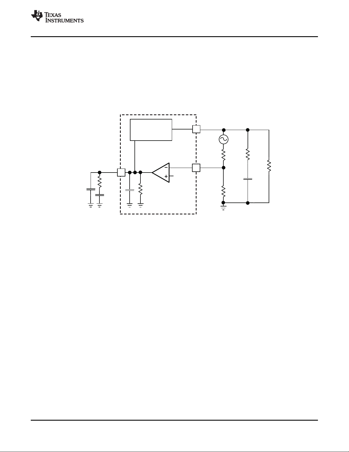
SMALL SIGNAL MODEL FOR LOOP RESPONSE
Figure 32 shows an equivalent model for the TPS54319 control loop which can be modeled in a circuit simulation
program to check frequency response and dynamic load response. The error amplifier is a transconductance
amplifier with a gm of 245 mA/V. The error amplifier can be modeled using an ideal voltage controlled current
source. The resistor Ro and capacitor Co model the open loop gain and frequency response of the amplifier. The
1-mV AC voltage source between the nodes a and b effectively breaks the control loop for the frequency
response measurements. Plotting a/c shows the small signal response of the frequency compensation. Plotting
a/b shows the small signal response of the overall loop. The dynamic loop response can be checked by
replacing the RLwith a current source with the appropriate load step amplitude and step rate in a time domain
analysis.
Figure 32. Small Signal Model for Loop Response
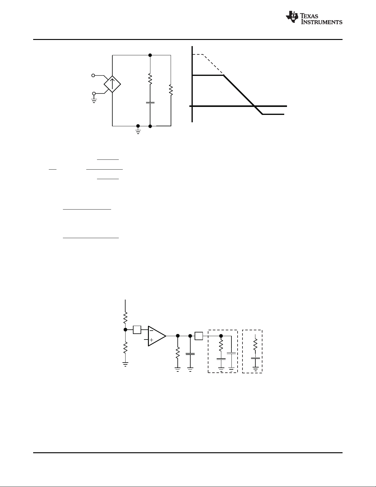
SIMPLE SMALL SIGNAL MODEL FOR PEAK CURRENT MODE CONTROL
Figure 32 is a simple small signal model that can be used to understand how to design the frequency
compensation. The TPS54319 power stage can be approximated to a voltage controlled current source (duty
cycle modulator) supplying current to the output capacitor and load resistor. The control to output transfer
function is shown in Equation 11 and consists of a dc gain, one dominant pole and one ESR zero. The quotient
of the change in switch current and the change in COMP pin voltage (node c in Figure 32) is the power stage
transconductance. The gm for the TPS54319 is 18.0 A/V. The low frequency gain of the power stage frequency
response is the product of the transconductance and the load resistance as shown in Equation 12. As the load
current increases and decreases, the low frequency gain decreases and increases, respectively. This variation
with load may seem problematic at first glance, but the dominant pole moves with load current [see Equation 13].
The combined effect is highlighted by the dashed line in the right half of Figure 33. As the load current
decreases, the gain increases and the pole frequency lowers, keeping the 0-dB crossover frequency the same
for the varying load conditions which makes it easier to design the frequency compensation.
vertical spacer
vertical spacer
Copyright © 2010, Texas Instruments Incorporated Submit Documentation Feedback 17
Product Folder Link(s): TPS54319
Page 18
VO
R
L
VC
fp
fz
Adc
gm
ps
R
ESR
C
OUT
s
1+
2 × z
vo
= Adc
vc
s
1+
2 × p
æ ö
ç ÷
p ¦
è ø
´
æ ö
ç ÷
p ¦
è ø
ps L
Adc = gm R´
¦
´ ´ p
OU T L
1
p =
C R 2
¦
´ ´ p
OUT ESR
1
z =
C R 2
Vref
VO
R1
R3
C1
C2
R2
CO
5pF
RO
gm
ea
COMP
VSENSE
Type 2A
Type 2 B
R3
C1
TPS54319
SLVSA83 –JUNE 2010
Figure 33. Simple Small Signal Model and Frequency Response for Peak Current Mode Control
www.ti.com
(11)
(12)
(13)
vertical spacer
(14)
SMALL SIGNAL MODEL FOR FREQUENCY COMPENSATION
The TPS54319 uses a transconductance amplifier for the error amplifier and readily supports two of the
commonly used frequency compensation circuits. The compensation circuits are shown in Figure 34. The Type 2
circuits are most likely implemented in high bandwidth power supply designs using low ESR output capacitors. In
Type 2A, one additional high frequency pole is added to attenuate high frequency noise.
Figure 34. Types of Frequency Compensation
18 Submit Documentation Feedback Copyright © 2010, Texas Instruments Incorporated
Product Folder Link(s): TPS54319
Page 19

¦
p ´ ´
Iout max
p mod =
2 Vout C out
¦
p ´ ´
1
z m o d =
2 Resr Co ut
¦ ¦ ´ ¦
C
= p mod z mod
¦
¦ ¦ ´
C
sw
= p mod
2
p ¦ ´ ´
´ ´
OUT
ea ps
2 × c Vo C
R3 =
gm Vref gm
¦
´ ´ p
OU T L
1
p =
C R 2
´
L OUT
R C
C1 =
R3
´
OUT
Resr C
C2 =
R3
TPS54319
www.ti.com
SLVSA83 –JUNE 2010
The design guidelines for TPS54319 loop compensation are as follows:
1. The modulator pole, fpmod, and the esr zero, fz1 must be calculated using Equation 15 and Equation 16.
Derating the output capacitor (C
) may be needed if the output voltage is a high percentage of the
OUT
capacitor rating. Use the capacitor manufacturer information to derate the capacitor value. Use Equation 17
and Equation 18 to estimate a starting point for the crossover frequency, fc. Equation 17 is the geometric
mean of the modulator pole and the esr zero and Equation 18 is the mean of modulator pole and the
switching frequency. Use the lower value of Equation 17 or Equation 18 as the maximum crossover
frequency.
(15)
vertical spacer
(16)
vertical spacer
(17)
vertical spacer
(18)
vertical spacer
2. R3 can be determined by
vertical spacer
Where is the gmeaamplifier gain (245 mA/V), gmpsis the power stage gain (18 A/V).
3. Place a compensation zero at the dominant pole . C1 can be determined by
vertical spacer
4. C2 is optional. It can be used to cancel the zero from Co’s ESR.
(19)
(20)
(21)
Copyright © 2010, Texas Instruments Incorporated Submit Documentation Feedback 19
Product Folder Link(s): TPS54319
Page 20

TPS54319
SLVSA83 –JUNE 2010
www.ti.com
APPLICATION INFORMATION
DESIGN GUIDE – STEP-BY-STEP DESIGN PROCEDURE
This example details the design of a high frequency switching regulator design using ceramic output capacitors.
This design is available as the HPA375 evaluation module (EVM). A few parameters must be known in order to
start the design process. These parameters are typically determined on the system level. For this example, we
start with the following known parameters:
Output Voltage 1.8 V
Transient Response 1 to 2A load step ΔVout = 5%
Maximum Output Current 3 A
Input Voltage 5 V nom. 3 V to 5 V
Output Voltage Ripple < 30 mV p-p
Switching Frequency (Fsw) 1000 kHz
SELECTING THE SWITCHING FREQUENCY
The first step is to decide on a switching frequency for the regulator. Typically, you want to choose the highest
switching frequency possible since this produces the smallest solution size. The high switching frequency allows
for lower valued inductors and smaller output capacitors compared to a power supply that switches at a lower
frequency. However, the highest switching frequency causes extra switching losses, which hurt the converter’s
performance. The converter is capable of running from 300 kHz to 2 MHz. Unless a small solution size is an
ultimate goal, a moderate switching frequency of 1MHz is selected to achieve both a small solution size and a
high efficiency operation. Using Equation 9, R5 is calculated to be 180 kΩ. A standard 1% 182 kΩ value was
chosen in the design.
Figure 35. High Frequency, 1.8 V Output Power Supply Design with Adjusted UVLO
OUTPUT INDUCTOR SELECTION
The inductor selected works for the entire TPS54319 input voltage range. To calculate the value of the output
inductor, use Equation 22. K
maximum output current. The inductor ripple current is filtered by the output capacitor. Therefore, choosing high
inductor ripple currents impacts the selection of the output capacitor since the output capacitor must have a
ripple current rating equal to or greater than the inductor ripple current. In general, the inductor ripple value is at
the discretion of the designer; however, K
20 Submit Documentation Feedback Copyright © 2010, Texas Instruments Incorporated
is a coefficient that represents the amount of inductor ripple current relative to the
IND
is normally from 0.1 to 0.3 for the majority of applications.
IND
Product Folder Link(s): TPS54319
Page 21

´
´ ´ ¦
Vinmax Vout Vout
L1 =
Io Kind Vinmax sw
´
´ ¦
Vinmax Vout Vout
Iripple =
L1 Vinmax sw
æ ö
´ -
´
ç ÷
´ ´ ¦
è ø
2
2
1 Vo (Vinm ax Vo)
ILrms = Io +
12 Vinmax L1 sw
Iripple
ILpeak = Iout +
2
2 Iout
Co >
sw Vout
´ D
¦ ´ D
TPS54319
www.ti.com
For this design example, use K
= 0.3 and the inductor value is calculated to be 1.36 mH. For this design, a
IND
SLVSA83 –JUNE 2010
nearest standard value was chosen: 1.5 mH. For the output filter inductor, it is important that the RMS current
and saturation current ratings not be exceeded. The RMS and peak inductor current can be found from
Equation 24 and Equation 25.
For this design, the RMS inductor current is 3.01 A and the peak inductor current is 3.72 A. The chosen inductor
is a Coilcraft XLA4020-152ME_. It has a saturation current rating 0f 9.6 A and a RMS current rating of 7.5 A.
The current flowing through the inductor is the inductor ripple current plus the output current. During power up,
faults or transient load conditions, the inductor current can increase above the calculated peak inductor current
level calculated above. In transient conditions, the inductor current can increase up to the switch current limit of
the device. For this reason, the most conservative approach is to specify an inductor with a saturation current
rating equal to or greater than the switch current limit rather than the peak inductor current.
(22)
vertical spacer
(23)
vertical spacer
(24)
vertical spacer
(25)
OUTPUT CAPACITOR
There are three primary considerations for selecting the value of the output capacitor. The output capacitor
determines the modulator pole, the output voltage ripple, and how the regulator responds to a large change in
load current. The output capacitance needs to be selected based on the more stringent of these three criteria.
The desired response to a large change in the load current is the first criteria. The output capacitor needs to
supply the load with current when the regulator can not. This situation would occur if there are desired hold-up
times for the regulator where the output capacitor must hold the output voltage above a certain level for a
specified amount of time after the input power is removed. The regulator is temporarily not able to supply
sufficient output current if there is a large, fast increase in the current needs of the load such as transitioning
from no load to a full load. The regulator usually needs two or more clock cycles for the control loop to see the
change in load current and output voltage and adjust the duty cycle to react to the change. The output capacitor
must be sized to supply the extra current to the load until the control loop responds to the load change. The
output capacitance must be large enough to supply the difference in current for 2 clock cycles while only allowing
a tolerable amount of droop in the output voltage. Equation 26 shows the minimum output capacitance necessary
to accomplish this.
For this example, the transient load response is specified as a 5 % change in Vout for a load step from 0 A (no
load) to 1.5 A (50% load). For this example, ΔIout = 1.5-0 = 1.5 A and ΔVout= 0.05 × 1.8 = 0.090 V. Using these
numbers gives a minimum capacitance of 33 mF. This value does not take the ESR of the output capacitor into
account in the output voltage change. For ceramic capacitors, the ESR is usually small enough to ignore in this
calculation.
Equation 27 calculates the minimum output capacitance needed to meet the output voltage ripple specification.
Where fsw is the switching frequency, Vripple is the maximum allowable output voltage ripple, and Iripple is the
inductor ripple current. In this case, the maximum output voltage ripple is 30 mV. Under this requirement,
Equation 27 yields 2.3 uF.
vertical spacer
Copyright © 2010, Texas Instruments Incorporated Submit Documentation Feedback 21
(26)
Product Folder Link(s): TPS54319
Page 22

1 1
Co >
Voripple
8 sw
Iripple
´
´ ¦
Voripple
Resr <
Iripple
´ -
´ ´ ´ ¦
Vo ut (Vinmax Vout)
Ico rm s =
12 Vinm ax L1 sw
( )
Vinmin Vout
Vout
Icirms = Iout
Vinmin Vinmin
-
´ ´
Ioutmax 0.25
Vin =
Cin sw
´
D
´ ¦
TPS54319
SLVSA83 –JUNE 2010
www.ti.com
vertical spacer
Where ΔIout is the change in output current, Fsw is the regulators switching frequency and ΔVout is the
allowable change in the output voltage. (27)
vertical spacer
Equation 28 calculates the maximum ESR an output capacitor can have to meet the output voltage ripple
specification. Equation 28 indicates the ESR should be less than 55 mΩ. In this case, the ESR of the ceramic
capacitor is much less than 55 mΩ.
Additional capacitance de-ratings for aging, temperature and DC bias should be factored in which increases this
minimum value. For this example, two 22 mF 10 V X5R ceramic capacitors with 3 mΩ of ESR are used.
Capacitors generally have limits to the amount of ripple current they can handle without failing or producing
excess heat. An output capacitor that can support the inductor ripple current must be specified. Some capacitor
data sheets specify the RMS (Root Mean Square) value of the maximum ripple current. Equation 29 can be used
to calculate the RMS ripple current the output capacitor needs to support. For this application, Equation 29 yields
333 mA.
(28)
vertical spacer
(29)
INPUT CAPACITOR
The TPS54319 requires a high quality ceramic, type X5R or X7R, input decoupling capacitor of at least 4.7 mF of
effective capacitance and in some applications a bulk capacitance. The effective capacitance includes any DC
bias effects. The voltage rating of the input capacitor must be greater than the maximum input voltage. The
capacitor must also have a ripple current rating greater than the maximum input current ripple of the TPS54319.
The input ripple current can be calculated using Equation 30.
The value of a ceramic capacitor varies significantly over temperature and the amount of DC bias applied to the
capacitor. The capacitance variations due to temperature can be minimized by selecting a dielectric material that
is stable over temperature. X5R and X7R ceramic dielectrics are usually selected for power regulator capacitors
because they have a high capacitance to volume ratio and are fairly stable over temperature. The output
capacitor must also be selected with the DC bias taken into account. The capacitance value of a capacitor
decreases as the DC bias across a capacitor increases.
For this example design, a ceramic capacitor with at least a 10 V voltage rating is required to support the
maximum input voltage. For this example, one 10 mF and one 0.1 mF 10 V capacitors in parallel have been
selected. The input capacitance value determines the input ripple voltage of the regulator. The input voltage
ripple can be calculated using Equation 31. Using the design example values, Ioutmax=3 A, Cin=10 mF, Fsw=1
MHz, yields an input voltage ripple of 76 mV and a rms input ripple current of 1.47 A.
(30)
vertical spacer
SLOW START CAPACITOR
The slow start capacitor determines the minimum amount of time it takes for the output voltage to reach its
22 Submit Documentation Feedback Copyright © 2010, Texas Instruments Incorporated
Product Folder Link(s): TPS54319
(31)
Page 23

Tss(ms) Iss( A)
Css(nF) =
Vref(V)
´ m
-
Vref
R7 = R6
Vo Vref
( ) ( )
Voutmin Ontimemin Fsmax Vinmax Ioutmin 2 RDS Ioutmin RL RDS= ´ ´ - ´ ´ - ´ +
( ) ( ) ( )
Voutmax 1 Offtimemax Fsmax Vinmin Ioutmax 2 RDS Ioutmax RL RDS= - ´ ´ - ´ ´ - ´ +
TPS54319
www.ti.com
SLVSA83 –JUNE 2010
nominal programmed value during power up. This is useful if a load requires a controlled voltage slew rate. This
is also used if the output capacitance is very large and would require large amounts of current to quickly charge
the capacitor to the output voltage level. The large currents necessary to charge the capacitor may make the
TPS54319 reach the current limit or excessive current draw from the input power supply may cause the input
voltage rail to sag. Limiting the output voltage slew rate solves both of these problems.
The slow start capacitor value can be calculated using Equation 32. For the example circuit, the slow start time is
not too critical since the output capacitor value is 44 mF which does not require much current to charge to 1.8 V.
The example circuit has the slow start time set to an arbitrary value of 4ms which requires a 10 nF capacitor. In
TPS54319, Iss is 2.2 mA and Vref is 0.827 V.
(32)
BOOTSTRAP CAPACITOR SELECTION
A 0.1 mF ceramic capacitor must be connected between the BOOT to PH pin for proper operation. It is
recommended to use a ceramic capacitor with X5R or better grade dielectric. The capacitor should have 10 V or
higher voltage rating.
OUTPUT VOLTAGE AND FEEDBACK RESISTORS SELECTION
For the example design, 100 kΩ was selected for R6. Using Equation 33, R7 is calculated as 80 kΩ. The nearest
standard 1% resistor is 80.5 kΩ.
(33)
Due to the internal design of the TPS54319, there is a minimum output voltage limit for any given input voltage.
The output voltage can never be lower than the internal voltage reference of 0.827 V. Above 0.827 V, the output
voltage may be limited by the minimum controllable on time. The minimum output voltage in this case is given by
Equation 34
Where:
Voutmin = minimum achievable output voltage
Ontimemin = minimum controllable on-time (65 ns typical. 120 nsec no load)
Fsmax = maximum switching frequency including tolerance
Vinmax = maximum input voltage
Ioutmin = minimum load current
RDS = minimum high side MOSFET on resistance (45 - 64 mΩ)
RL = series resistance of output inductor (34)
There is also a maximum achievable output voltage which is limited by the minimum off time. The maximum
output voltage is given by Equation 35
Where:
Voutmax = maximum achievable output voltage
Offtimeman = maximum off time (60 nsec typical)
Fsmax = maximum switching frequency including tolerance
Vinmin = minimum input voltage
Ioutmax = maximum load current
RDS = maximum high side MOSFET on resistance (81 - 110 mΩ)
RL = series resistance of output inductor (35)
Copyright © 2010, Texas Instruments Incorporated Submit Documentation Feedback 23
Product Folder Link(s): TPS54319
Page 24

¦
p ´ ´
Iout max
p mod =
2 Vout C out
¦
p ´ ´
1
z m o d =
2 Resr Co ut
¦ ¦ ´ ¦
C
= p mod z mod
¦
¦ ¦ ´
C
sw
= p mod
2
gm
2 × c Vo Co
R3 =
Gm Vref VI
p ¦ ´ ´
´ ´
´Ro Co
C3 =
R3
TPS54319
SLVSA83 –JUNE 2010
www.ti.com
COMPENSATION
There are several industry techniques used to compensate DC/DC regulators. The method presented here is
easy to calculate and yields high phase margins. For most conditions, the regulator has a phase margin between
60 and 90 degrees. The method presented here ignores the effects of the slope compensation that is internal to
the TPS54319. Since the slope compensation is ignored, the actual cross over frequency is usually lower than
the cross over frequency used in the calculations. Use SwitcherPro software for a more accurate design.
To get started, the modulator pole, fpmod, and the esr zero, fz1 must be calculated using Equation 36 and
Equation 37. For Cout, derating the capacitor is not needed as the 1.8 V output is a small percentage of the 10 V
capacitor rating. If the output is a high percentage of the capacitor rating, use the capacitor manufacturer
information to derate the capacitor value. Use Equation 38 and Equation 39 to estimate a starting point for the
crossover frequency, fc. For the example design, fpmod is 6.03 kHz and fzmod is 1210 kHz. Equation 38 is the
geometric mean of the modulator pole and the esr zero and Equation 39 is the mean of modulator pole and the
switching frequency. Equation 38 yields 85.3 kHz and Equation 39 gives 54.9 kHz. Use the lower value of
Equation 38 or Equation 39 as the approximate crossover frequency. For this example, fc is 56 kHz. Next, the
compensation components are calculated. A resistor in series with a capacitor is used to create a compensating
zero. A capacitor in parallel to these two components forms the compensating pole (if needed).
(36)
vertical spacer
(37)
vertical spacer
(38)
vertical spacer
(39)
vertical spacer
The compensation design takes the following steps:
1. Set up the anticipated cross-over frequency. Use Equation 40 to calculate the compensation network’s
resistor value. In this example, the anticipated cross-over frequency (fc) is 56 kHz. The power stage gain
(gmps) is 18 A/V and the error amplifier gain (gmea) is 245 mA/V.
(40)
2. Place compensation zero at the pole formed by the load resistor and the output capacitor. The compensation
network’s capacitor can be calculated from Equation 41.
(41)
3. An additional pole can be added to attenuate high frequency noise. In this application, it is not necessary to
add it.
From the procedures above, the compensation network includes a 7.68 kΩ resistor and a 3300 pF capacitor.
24 Submit Documentation Feedback Copyright © 2010, Texas Instruments Incorporated
Product Folder Link(s): TPS54319
Page 25

3.3 Vin,1.8 Vout
5 Vin, 1.8 Vout
0.001 0.01 0.1 1 10
Output Current - A
0
10
20
30
40
50
60
70
80
90
100
Efficiency - %
40
50
60
70
80
90
0
10
20
30
100
Efficiency - %
0 0.5 2 2.5 3
Output Current - A
1 1.5
5 Vin, 1.8 Vout
3.3 Vin,1.8 Vout
1.05V
1.2V
1.5V
1.8V
2.5V
50
55
60
65
70
75
80
85
90
95
100
Efficience-%
0 0.5 1 1.5 2 2.5 3
I -OutputCurrent- A
O
50
55
60
65
70
75
80
85
90
95
100
0 0.5 1 1.5 2 2.5 3
I -OutputCurrent- A
O
1.05V
1.2V
1.5V
1.8V
2.5V
3.3V
Efficience-%
Vin=5V/div
Vout=2V/div
EN=2V/div
PWRGD=5V/div
Time=5msec/div
Vout=100mV/div(accoupled)
Iout=1 A /div(0 A to1.5 A loadstep)
Time=200usec/div
TPS54319
www.ti.com
APPLICATION CURVES
EFFICIENCY EFFICIENCY
LOAD CURRENT LOAD CURRENT
Figure 36. Figure 37.
EFFICIENCY EFFICIENCY
LOAD CURRENT LOAD CURRENT
1 MHz, 3.3 VIN, TA= 25°C 1 MHz, 5 VIN, TA= 25°C
SLVSA83 –JUNE 2010
vs vs
vs vs
Figure 38. Figure 39.
TRANSIENT RESPONSE, 1.5 A STEP POWER UP VOUT, VIN
Figure 40. Figure 41.
Copyright © 2010, Texas Instruments Incorporated Submit Documentation Feedback 25
Product Folder Link(s): TPS54319
Page 26
Vin=5V/div
Vout=2V/div
EN=2V/div
PWRGD=5V/div
Time=5msec/div
Vout=20mV/div(accoupled)
PH=2V/div
Time=500nsec/div
Vin=100mV/div(accoupled)
PH=2V/div
Time=500nsec/div
10 100 1000 10k 100k 1M
Frequency - Hz
–60
Gain - dB
50
40
30
20
10
0
–10
–20
–30
–40
–50
60
Phase - Degrees
150
120
90
60
30
0
–30
–60
–90
–120
–150
–180
180
Phase
Gain
3 3.5 5 6
Input Voltage-V
Iout = 2 A
-0.4
-0.3
-0.2
-0.1
0
0.1
0.2
0.3
0.4
Output Voltage Deviation - %
4. 5 5.54
Vin = 3.3 V
-0.4
-0.3
-0.2
-0.1
0
0.1
0.2
0.3
0.4
Output Voltage Deviation - %
0 0.5 2 2.5 3
Output Current - A
1 1.5
Vin = 5 V
TPS54319
SLVSA83 –JUNE 2010
www.ti.com
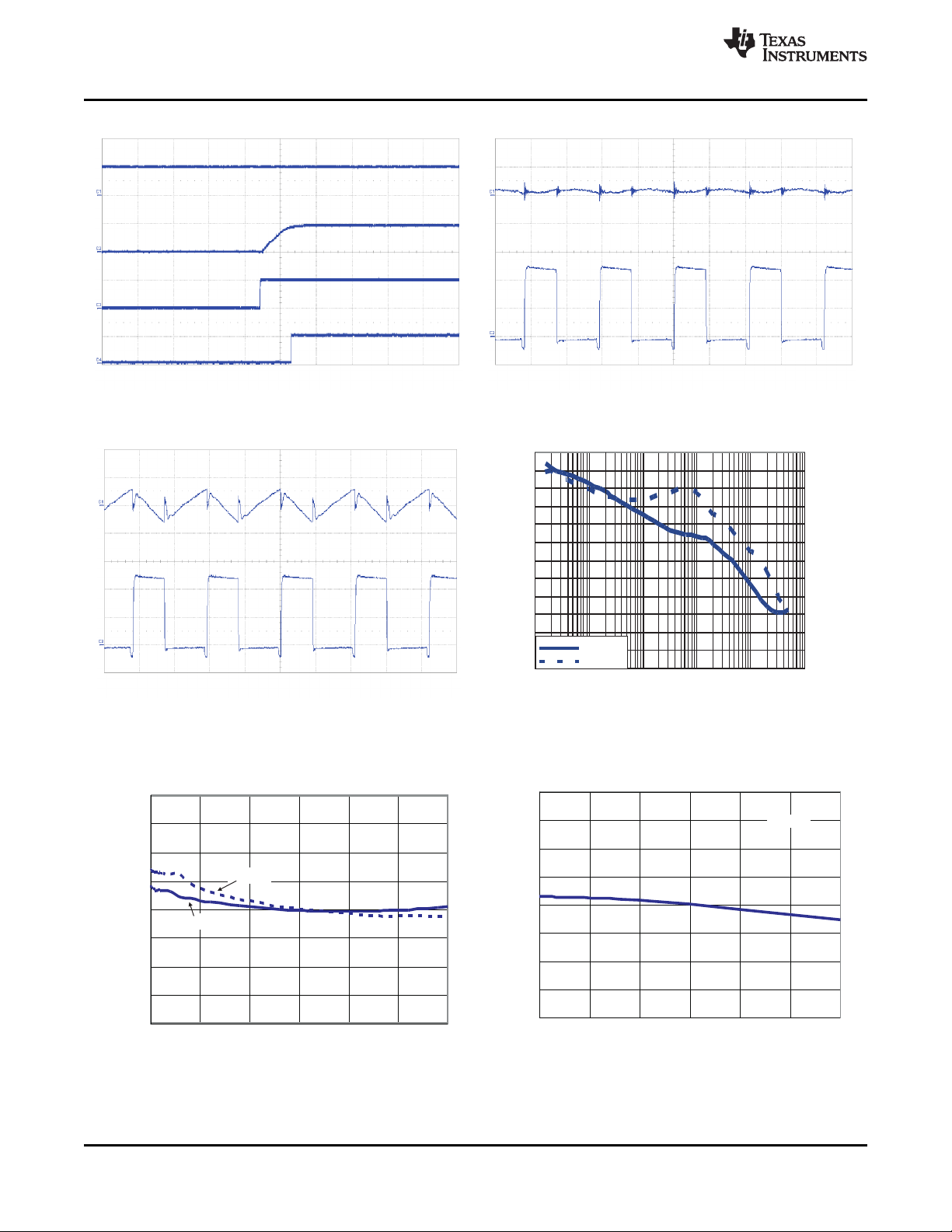
POWER UP VOUT, EN OUTPUT RIPPLE, 3 A
Figure 42. Figure 43.
INPUT RIPPLE, 3 A CLOSED LOOP RESPONSE, VIN (5 V), 3 A
Figure 44. Figure 45.
LOAD REGULATION REGULATION
LOAD CURRENT INPUT VOLTAGE
26 Submit Documentation Feedback Copyright © 2010, Texas Instruments Incorporated
Figure 46. Figure 47.
vs vs
Product Folder Link(s): TPS54319
Page 27

TPS54319
www.ti.com
SLVSA83 –JUNE 2010
POWER DISSIPATION ESTIMATE
The following formulas show how to estimate the IC power dissipation under continuous conduction mode (CCM)
operation. The power dissipation of the IC (Ptot) includes conduction loss (Pcon), dead time loss (Pd), switching
loss (Psw), gate drive loss (Pgd) and supply current loss (Pq).
Pcon = Io2× R
Pd = ƒsw× Io × 0.7 × 40 × 10
Psw = 1/2 × Vin× Io × ƒsw× 8 × 10
Pgd = 2 × Vin× ƒsw× 2 × 10
Pq = Vin× 360 × 10
Where:
IOis the output current (A).
R
DS_on_Temp
Vinis the input voltage (V).
ƒswis the switching frequency (Hz).
So
Ptot = Pcon + Pd + Psw + Pgd + Pq
For given TA,
TJ = TA + Rth × Ptot
For given TJMAX = 150°C
TAmax = TJ max – Rth × Ptot
Where:
Ptot is the total device power dissipation (W).
TA is the ambient temperature (°C).
TJ is the junction temperature (°C).
Rth is the thermal resistance of the package (°C/W).
TJMAX is maximum junction temperature (°C).
TAMAX is maximum ambient temperature (°C).
DS_on_Temp
–9
–9
–9
–6
is the on-resistance of the high-side MOSFET with given temperature (Ω).
There are additional power losses in the regulator circuit due to the inductor AC and DC losses and trace
resistance that impact the overall efficiency of the regulator.
LAYOUT
Layout is a critical portion of good power supply design. There are several signal paths that conduct fast
changing currents or voltages that can interact with stray inductance or parasitic capacitance to generate noise
or degrade the power supplies performance. Care should be taken to minimize the loop area formed by the
bypass capacitor connections and the VIN pins. See Figure 48 for a PCB layout example. The GND pins and
AGND pin should be tied directly to the power pad under the IC. The power pad should be connected to any
internal PCB ground planes using multiple vias directly under the IC. Additional vias can be used to connect the
top side ground area to the internal planes near the input and output capacitors. For operation at full rated load,
the top side ground area along with any additional internal ground planes must provide adequate heat dissipating
area.
Locate the input bypass capacitor as close to the IC as possible. The PH pin should be routed to the output
inductor. Since the PH connection is the switching node, the output inductor should be located very close to the
PH pins, and the area of the PCB conductor minimized to prevent excessive capacitive coupling. The boot
capacitor must also be located close to the device. The sensitive analog ground connections for the feedback
Copyright © 2010, Texas Instruments Incorporated Submit Documentation Feedback 27
Product Folder Link(s): TPS54319
Page 28

VIN
VIN
VIN
GND
EN
GND
VSENSE
SS
PH
PH
PH
PWRGD
BOOT
RT/CLK
COMP
AGND
PH
BOOT
CAPACITOR
VOUT
OUTPUT
INDUCTOR
OUTPUT
FILTER
CAPACITOR
SLOW START
CAPACITOR
COMPENSATION
NETWORK
TOPSIDE
GROUND
AREA
VIA to Ground Plane
FREQUENCY
SET
RESISTOR
ANALOG
GROUND
TRACE
VIN
INPUT
BYPASS
CAPACITOR
VIN
UVLO SET
RESISTORS
FEEDBACK
RESISTORS
VIA to
Ground
Plane
EXPOSED
POWERPAD
AREA
TPS54319
SLVSA83 –JUNE 2010
www.ti.com
voltage divider, compensation components, slow start capacitor and frequency set resistor should be connected
to a separate analog ground trace as shown. The RT/CLK pin is particularly sensitive to noise so the RT resistor
should be located as close as possible to the IC and routed with minimal lengths of trace. The additional external
components can be placed approximately as shown. It may be possible to obtain acceptable performance with
alternate PCB layouts, however this layout has been shown to produce good results and is meant as a guideline.
Figure 48. PCB Layout Example
28 Submit Documentation Feedback Copyright © 2010, Texas Instruments Incorporated
Product Folder Link(s): TPS54319
Page 29
PACKAGE OPTION ADDENDUM
www.ti.com
23-Feb-2014
PACKAGING INFORMATION
Orderable Device Status
TPS54319RTER ACTIVE WQFN RTE 16 3000 Green (RoHS
TPS54319RTET ACTIVE WQFN RTE 16 250 Green (RoHS
(1)
The marketing status values are defined as follows:
ACTIVE: Product device recommended for new designs.
LIFEBUY: TI has announced that the device will be discontinued, and a lifetime-buy period is in effect.
NRND: Not recommended for new designs. Device is in production to support existing customers, but TI does not recommend using this part in a new design.
PREVIEW: Device has been announced but is not in production. Samples may or may not be available.
OBSOLETE: TI has discontinued the production of the device.
Package Type Package
(1)
Drawing
Pins Package
Qty
Eco Plan
(2)
& no Sb/Br)
& no Sb/Br)
Lead/Ball Finish
(6)
CU NIPDAU Level-2-260C-1 YEAR -40 to 150 54319
CU NIPDAU Level-2-260C-1 YEAR -40 to 150 54319
MSL Peak Temp
(3)
Op Temp (°C) Device Marking
(4/5)
(2)
Eco Plan - The planned eco-friendly classification: Pb-Free (RoHS), Pb-Free (RoHS Exempt), or Green (RoHS & no Sb/Br) - please check http://www.ti.com/productcontent for the latest availability
information and additional product content details.
TBD: The Pb-Free/Green conversion plan has not been defined.
Pb-Free (RoHS): TI's terms "Lead-Free" or "Pb-Free" mean semiconductor products that are compatible with the current RoHS requirements for all 6 substances, including the requirement that
lead not exceed 0.1% by weight in homogeneous materials. Where designed to be soldered at high temperatures, TI Pb-Free products are suitable for use in specified lead-free processes.
Pb-Free (RoHS Exempt): This component has a RoHS exemption for either 1) lead-based flip-chip solder bumps used between the die and package, or 2) lead-based die adhesive used between
the die and leadframe. The component is otherwise considered Pb-Free (RoHS compatible) as defined above.
Green (RoHS & no Sb/Br): TI defines "Green" to mean Pb-Free (RoHS compatible), and free of Bromine (Br) and Antimony (Sb) based flame retardants (Br or Sb do not exceed 0.1% by weight
in homogeneous material)
(3)
MSL, Peak Temp. - The Moisture Sensitivity Level rating according to the JEDEC industry standard classifications, and peak solder temperature.
(4)
There may be additional marking, which relates to the logo, the lot trace code information, or the environmental category on the device.
(5)
Multiple Device Markings will be inside parentheses. Only one Device Marking contained in parentheses and separated by a "~" will appear on a device. If a line is indented then it is a continuation
of the previous line and the two combined represent the entire Device Marking for that device.
(6)
Lead/Ball Finish - Orderable Devices may have multiple material finish options. Finish options are separated by a vertical ruled line. Lead/Ball Finish values may wrap to two lines if the finish
value exceeds the maximum column width.
Important Information and Disclaimer:The information provided on this page represents TI's knowledge and belief as of the date that it is provided. TI bases its knowledge and belief on information
provided by third parties, and makes no representation or warranty as to the accuracy of such information. Efforts are underway to better integrate information from third parties. TI has taken and
continues to take reasonable steps to provide representative and accurate information but may not have conducted destructive testing or chemical analysis on incoming materials and chemicals.
TI and TI suppliers consider certain information to be proprietary, and thus CAS numbers and other limited information may not be available for release.
Samples
Addendum-Page 1
Page 30
PACKAGE OPTION ADDENDUM
www.ti.com
In no event shall TI's liability arising out of such information exceed the total purchase price of the TI part(s) at issue in this document sold by TI to Customer on an annual basis.
23-Feb-2014
Addendum-Page 2
Page 31
PACKAGE MATERIALS INFORMATION
www.ti.com 14-Jul-2012
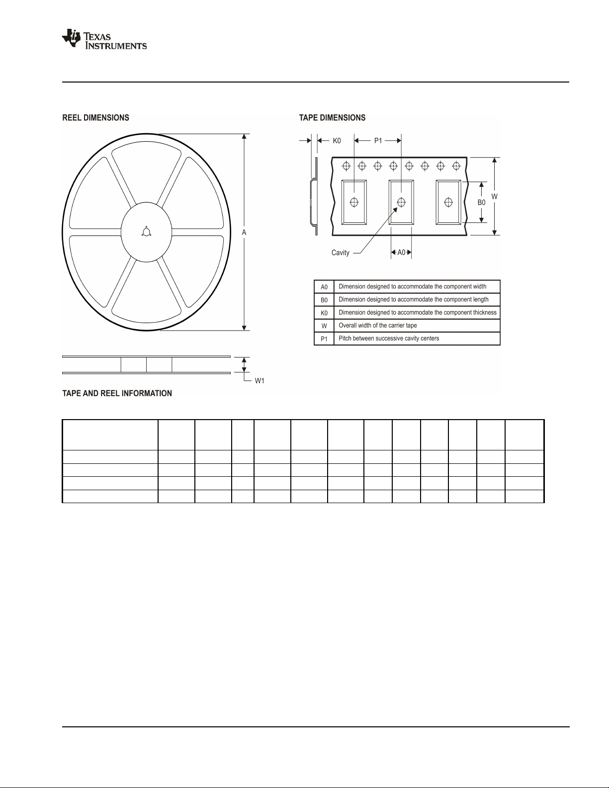
TAPE AND REEL INFORMATION
*All dimensions are nominal
Device Package
TPS54319RTER WQFN RTE 16 3000 330.0 12.4 3.3 3.3 1.1 8.0 12.0 Q2
TPS54319RTER WQFN RTE 16 3000 330.0 12.4 3.3 3.3 1.1 8.0 12.0 Q2
TPS54319RTET WQFN RTE 16 250 180.0 12.4 3.3 3.3 1.1 8.0 12.0 Q2
TPS54319RTET WQFN RTE 16 250 180.0 12.4 3.3 3.3 1.1 8.0 12.0 Q2
Type
Package
Drawing
Pins SPQ Reel
Diameter
(mm)
Reel
Width
W1 (mm)
A0
(mm)B0(mm)K0(mm)P1(mm)W(mm)
Pin1
Quadrant
Pack Materials-Page 1
Page 32

PACKAGE MATERIALS INFORMATION
www.ti.com 14-Jul-2012
*All dimensions are nominal
Device Package Type Package Drawing Pins SPQ Length (mm) Width (mm) Height (mm)
TPS54319RTER WQFN RTE 16 3000 367.0 367.0 35.0
TPS54319RTER WQFN RTE 16 3000 367.0 367.0 35.0
TPS54319RTET WQFN RTE 16 250 210.0 185.0 35.0
TPS54319RTET WQFN RTE 16 250 210.0 185.0 35.0
Pack Materials-Page 2
Page 33

Page 34

Page 35

Page 36

IMPORTANT NOTICE
Texas Instruments Incorporated and its subsidiaries (TI) reserve the right to make corrections, enhancements, improvements and other
changes to its semiconductor products and services per JESD46, latest issue, and to discontinue any product or service per JESD48, latest
issue. Buyers should obtain the latest relevant information before placing orders and should verify that such information is current and
complete. All semiconductor products (also referred to herein as “components”) are sold subject to TI’s terms and conditions of sale
supplied at the time of order acknowledgment.
TI warrants performance of its components to the specifications applicable at the time of sale, in accordance with the warranty in TI’s terms
and conditions of sale of semiconductor products. Testing and other quality control techniques are used to the extent TI deems necessary
to support this warranty. Except where mandated by applicable law, testing of all parameters of each component is not necessarily
performed.
TI assumes no liability for applications assistance or the design of Buyers’ products. Buyers are responsible for their products and
applications using TI components. To minimize the risks associated with Buyers’ products and applications, Buyers should provide
adequate design and operating safeguards.
TI does not warrant or represent that any license, either express or implied, is granted under any patent right, copyright, mask work right, or
other intellectual property right relating to any combination, machine, or process in which TI components or services are used. Information
published by TI regarding third-party products or services does not constitute a license to use such products or services or a warranty or
endorsement thereof. Use of such information may require a license from a third party under the patents or other intellectual property of the
third party, or a license from TI under the patents or other intellectual property of TI.
Reproduction of significant portions of TI information in TI data books or data sheets is permissible only if reproduction is without alteration
and is accompanied by all associated warranties, conditions, limitations, and notices. TI is not responsible or liable for such altered
documentation. Information of third parties may be subject to additional restrictions.
Resale of TI components or services with statements different from or beyond the parameters stated by TI for that component or service
voids all express and any implied warranties for the associated TI component or service and is an unfair and deceptive business practice.
TI is not responsible or liable for any such statements.
Buyer acknowledges and agrees that it is solely responsible for compliance with all legal, regulatory and safety-related requirements
concerning its products, and any use of TI components in its applications, notwithstanding any applications-related information or support
that may be provided by TI. Buyer represents and agrees that it has all the necessary expertise to create and implement safeguards which
anticipate dangerous consequences of failures, monitor failures and their consequences, lessen the likelihood of failures that might cause
harm and take appropriate remedial actions. Buyer will fully indemnify TI and its representatives against any damages arising out of the use
of any TI components in safety-critical applications.
In some cases, TI components may be promoted specifically to facilitate safety-related applications. With such components, TI’s goal is to
help enable customers to design and create their own end-product solutions that meet applicable functional safety standards and
requirements. Nonetheless, such components are subject to these terms.
No TI components are authorized for use in FDA Class III (or similar life-critical medical equipment) unless authorized officers of the parties
have executed a special agreement specifically governing such use.
Only those TI components which TI has specifically designated as military grade or “enhanced plastic” are designed and intended for use in
military/aerospace applications or environments. Buyer acknowledges and agrees that any military or aerospace use of TI components
which have not been so designated is solely at the Buyer's risk, and that Buyer is solely responsible for compliance with all legal and
regulatory requirements in connection with such use.
TI has specifically designated certain components as meeting ISO/TS16949 requirements, mainly for automotive use. In any case of use of
non-designated products, TI will not be responsible for any failure to meet ISO/TS16949.
Products Applications
Audio www.ti.com/audio Automotive and Transportation www.ti.com/automotive
Amplifiers amplifier.ti.com Communications and Telecom www.ti.com/communications
Data Converters dataconverter.ti.com Computers and Peripherals www.ti.com/computers
DLP® Products www.dlp.com Consumer Electronics www.ti.com/consumer-apps
DSP dsp.ti.com Energy and Lighting www.ti.com/energy
Clocks and Timers www.ti.com/clocks Industrial www.ti.com/industrial
Interface interface.ti.com Medical www.ti.com/medical
Logic logic.ti.com Security www.ti.com/security
Power Mgmt power.ti.com Space, Avionics and Defense www.ti.com/space-avionics-defense
Microcontrollers microcontroller.ti.com Video and Imaging www.ti.com/video
RFID www.ti-rfid.com
OMAP Applications Processors www.ti.com/omap TI E2E Community e2e.ti.com
Wireless Connectivity www.ti.com/wirelessconnectivity
Mailing Address: Texas Instruments, Post Office Box 655303, Dallas, Texas 75265
Copyright © 2014, Texas Instruments Incorporated
Page 37

 Loading...