

Page 1

EN
This Datasheet is presented by
the manufacturer
DE
Dieses Datenblatt wird vom
Hersteller bereitgestellt
FR
Cette fiche technique est
présentée par le fabricant
EN - For pricing and availability in your local country please visit one of the below links:
DE - Informationen zu Preisen und Verfügbarkeit in Ihrem Land erhalten Sie über die unten aufgeführten Links:
FR - Pour connaître les tarifs et la disponibilité dans votre pays, cliquez sur l'un des liens suivants:
TPS54310EVM
Page 2
User’s Guide
February 2002 PMP EVMs
SLLU037
Page 3
IMPORTANT NOTICE
Texas Instruments Incorporated and its subsidiaries (TI) reserve the right to make corrections, modifications,
enhancements, improvements, and other changes to its products and services at any time and to discontinue
any product or service without notice. Customers should obtain the latest relevant information before placing
orders and should verify that such information is current and complete. All products are sold subject to TI’s terms
and conditions of sale supplied at the time of order acknowledgment.
TI warrants performance of its hardware products to the specifications applicable at the time of sale in
accordance with TI’s standard warranty . Testing and other quality control techniques are used to the extent TI
deems necessary to support this warranty . Except where mandated by government requirements, testing of all
parameters of each product is not necessarily performed.
TI assumes no liability for applications assistance or customer product design. Customers are responsible for
their products and applications using TI components. T o minimize the risks associated with customer products
and applications, customers should provide adequate design and operating safeguards.
TI does not warrant or represent that any license, either express or implied, is granted under any TI patent right,
copyright, mask work right, or other TI intellectual property right relating to any combination, machine, or process
in which TI products or services are used. Information published by TI regarding third–party products or services
does not constitute a license from TI to use such products or services or a warranty or endorsement thereof.
Use of such information may require a license from a third party under the patents or other intellectual property
of the third party , or a license from TI under the patents or other intellectual property of TI.
Reproduction of information in TI data books or data sheets is permissible only if reproduction is without
alteration and is accompanied by all associated warranties, conditions, limitations, and notices. Reproduction
of this information with alteration is an unfair and deceptive business practice. TI is not responsible or liable for
such altered documentation.
Resale of TI products or services with statements different from or beyond the parameters stated by TI for that
product or service voids all express and any implied warranties for the associated TI product or service and
is an unfair and deceptive business practice. TI is not responsible or liable for any such statements.
Mailing Address:
Texas Instruments
Post Office Box 655303
Dallas, Texas 75265
Copyright 2002, Texas Instruments Incorporated
Page 4
EVM IMPORTANT NOTICE
Texas Instruments (TI) provides the enclosed product(s) under the following conditions:
This evaluation kit being sold by TI is intended for use for ENGINEERING DEVELOPMENT OR EV ALUA TION
PURPOSES ONL Y and is not considered by TI to be fit for commercial use. As such, the goods being provided
may not be complete in terms of required design-, marketing-, and/or manufacturing-related protective
considerations, including product safety measures typically found in the end product incorporating the goods.
As a prototype, this product does not fall within the scope of the European Union directive on electromagnetic
compatibility and therefore may not meet the technical requirements of the directive.
Should this evaluation kit not meet the specifications indicated in the EVM User’s Guide, the kit may be returned
within 30 days from the date of delivery for a full refund. THE FOREGOING WARRANTY IS THE EXCLUSIVE
WARRANTY MADE BY SELLER TO BUYER AND IS IN LIEU OF ALL OTHER WARRANTIES, EXPRESSED,
IMPLIED, OR ST ATUT ORY, INCLUDING ANY W ARRANTY OF MERCHANTABILITY OR FITNESS FOR ANY
PARTICULAR PURPOSE.
The user assumes all responsibility and liability for proper and safe handling of the goods. Further, the user
indemnifies TI from all claims arising from the handling or use of the goods. Please be aware that the products
received may not be regulatory compliant or agency certified (FCC, UL, CE, etc.). Due to the open construction
of the product, it is the user’s responsibility to take any and all appropriate precautions with regard to electrostatic
discharge.
EXCEPT TO THE EXTENT OF THE INDEMNITY SET FORTH ABOVE, NEITHER P ARTY SHALL BE LIABLE
TO THE OTHER FOR ANY INDIRECT, SPECIAL, INCIDENTAL, OR CONSEQUENTIAL DAMAGES.
TI currently deals with a variety of customers for products, and therefore our arrangement with the user is not
exclusive.
TI assumes no liability for applications assistance, customer product design, software performance, or
infringement of patents or services described herein.
Please read the EVM User’s Guide and, specifically, the EVM Warnings and Restrictions notice in the EVM
User’s Guide prior to handling the product. This notice contains important safety information about temperatures
and voltages. For further safety concerns, please contact the TI application engineer.
Persons handling the product must have electronics training and observe good laboratory practice standards.
No license is granted under any patent right or other intellectual property right of TI covering or relating to any
machine, process, or combination in which such TI products or services might be or are used.
Mailing Address:
Texas Instruments
Post Office Box 655303
Dallas, Texas 75265
Copyright 2002, Texas Instruments Incorporated
Page 5
EVM WARNINGS AND RESTRICTIONS
This EVM is designed to operate over an input voltage range of 4.0 V to 6.0 V , and over a load
range of 0 A to 3 A.
It is important to operate this EVM within the specified input and output ranges described in
the EVM User’s Guide.
Exceeding the specified input range may cause unexpected operation and/or irreversible
damage to the EVM. If there are questions concerning the input range, please contact a TI
field representative prior to connecting the input power.
Applying loads outside of the specified output range may result in unintended operation and/or
possible permanent damage to the EVM. Please consult the EVM User’s Guide prior to
connecting any load to the EVM output. If there is uncertainty as to the load specification,
please contact a TI field representative.
During normal operation, some circuit components may have case temperatures greater than
60°C. The EVM is designed to operate properly with certain components above 60°C as long
as the input and output ranges are maintained. These components include but are not limited
to linear regulators, switching transistors, pass transistors, and current sense resistors. These
types of devices can be identified using the EVM schematic located in the EVM User’s Guide.
When placing measurement probes near these devices during operation, please be aware
that these devices may be very warm to the touch.
Mailing Address:
Texas Instruments
Post Office Box 655303
Dallas, Texas 75265
Copyright 2002, Texas Instruments Incorporated
Page 6
Contents
Contents
1 Introduction 1-1. . . . . . . . . . . . . . . . . . . . . . . . . . . . . . . . . . . . . . . . . . . . . . . . . . . . . . . . . . . . . . . . . . . . .
1.1 Background 1-2. . . . . . . . . . . . . . . . . . . . . . . . . . . . . . . . . . . . . . . . . . . . . . . . . . . . . . . . . . . . . . . .
1.2 Performance Specification Summary 1-2. . . . . . . . . . . . . . . . . . . . . . . . . . . . . . . . . . . . . . . . . .
1.3 Modifications 1-3. . . . . . . . . . . . . . . . . . . . . . . . . . . . . . . . . . . . . . . . . . . . . . . . . . . . . . . . . . . . . . .
1.3.1 General 1-3. . . . . . . . . . . . . . . . . . . . . . . . . . . . . . . . . . . . . . . . . . . . . . . . . . . . . . . . . . . .
1.3.2 Switching Frequency 1-3. . . . . . . . . . . . . . . . . . . . . . . . . . . . . . . . . . . . . . . . . . . . . . . . .
1.3.3 Output Voltage 1-4. . . . . . . . . . . . . . . . . . . . . . . . . . . . . . . . . . . . . . . . . . . . . . . . . . . . . .
1.3.4 Slow Start 1-4. . . . . . . . . . . . . . . . . . . . . . . . . . . . . . . . . . . . . . . . . . . . . . . . . . . . . . . . . .
1.3.5 Improving Transient Response 1-4. . . . . . . . . . . . . . . . . . . . . . . . . . . . . . . . . . . . . . . .
2 Test Setup and Results 2-1. . . . . . . . . . . . . . . . . . . . . . . . . . . . . . . . . . . . . . . . . . . . . . . . . . . . . . . . . .
2.1 Input/Output Connections 2-2. . . . . . . . . . . . . . . . . . . . . . . . . . . . . . . . . . . . . . . . . . . . . . . . . . . .
2.2 Loop Characterization Setup 2-3. . . . . . . . . . . . . . . . . . . . . . . . . . . . . . . . . . . . . . . . . . . . . . . . .
2.3 Efficiency 2-3. . . . . . . . . . . . . . . . . . . . . . . . . . . . . . . . . . . . . . . . . . . . . . . . . . . . . . . . . . . . . . . . . .
2.4 Thermal Performance 2-4. . . . . . . . . . . . . . . . . . . . . . . . . . . . . . . . . . . . . . . . . . . . . . . . . . . . . . .
2.5 Output Voltage Regulation 2-5. . . . . . . . . . . . . . . . . . . . . . . . . . . . . . . . . . . . . . . . . . . . . . . . . . .
2.6 Load Transients 2-6. . . . . . . . . . . . . . . . . . . . . . . . . . . . . . . . . . . . . . . . . . . . . . . . . . . . . . . . . . . .
2.7 Loop Characteristics 2-7. . . . . . . . . . . . . . . . . . . . . . . . . . . . . . . . . . . . . . . . . . . . . . . . . . . . . . . .
2.8 Output Voltage Ripple 2-8. . . . . . . . . . . . . . . . . . . . . . . . . . . . . . . . . . . . . . . . . . . . . . . . . . . . . . .
2.9 Input Ripple Voltage 2-9. . . . . . . . . . . . . . . . . . . . . . . . . . . . . . . . . . . . . . . . . . . . . . . . . . . . . . . .
2.10 Start-Up 2-10. . . . . . . . . . . . . . . . . . . . . . . . . . . . . . . . . . . . . . . . . . . . . . . . . . . . . . . . . . . . . . . . . .
3 Board Layout 3-1. . . . . . . . . . . . . . . . . . . . . . . . . . . . . . . . . . . . . . . . . . . . . . . . . . . . . . . . . . . . . . . . . . .
3.1 Layout 3-2. . . . . . . . . . . . . . . . . . . . . . . . . . . . . . . . . . . . . . . . . . . . . . . . . . . . . . . . . . . . . . . . . . . .
4 Schematic and Bill of Materials 4-1. . . . . . . . . . . . . . . . . . . . . . . . . . . . . . . . . . . . . . . . . . . . . . . . . . .
4.1 Schematic 4-2. . . . . . . . . . . . . . . . . . . . . . . . . . . . . . . . . . . . . . . . . . . . . . . . . . . . . . . . . . . . . . . . .
4.2 Bill of Materials 4-3. . . . . . . . . . . . . . . . . . . . . . . . . . . . . . . . . . . . . . . . . . . . . . . . . . . . . . . . . . . . .
v
Page 7
Contents
Figures
1–1 Frequency Trimming Resistor Selection Graph 1-3. . . . . . . . . . . . . . . . . . . . . . . . . . . . . . . . . . . .
2–1 Connection Diagram 2-2. . . . . . . . . . . . . . . . . . . . . . . . . . . . . . . . . . . . . . . . . . . . . . . . . . . . . . . . . . .
2–2 Measured Efficiency 2-3. . . . . . . . . . . . . . . . . . . . . . . . . . . . . . . . . . . . . . . . . . . . . . . . . . . . . . . . . . .
2–3 Measured Board Losses 2-4. . . . . . . . . . . . . . . . . . . . . . . . . . . . . . . . . . . . . . . . . . . . . . . . . . . . . . .
°
2–4 Measured Junction Temperature at 25
2–5 Measured Load Regulation 2-5. . . . . . . . . . . . . . . . . . . . . . . . . . . . . . . . . . . . . . . . . . . . . . . . . . . . .
2–6 Measured Load Transient Response 2-6. . . . . . . . . . . . . . . . . . . . . . . . . . . . . . . . . . . . . . . . . . . .
2–7 Improved Load Transient Response 2-6. . . . . . . . . . . . . . . . . . . . . . . . . . . . . . . . . . . . . . . . . . . . .
2–8 Improved Loop Gain and Phase 2-7. . . . . . . . . . . . . . . . . . . . . . . . . . . . . . . . . . . . . . . . . . . . . . . . .
2–9 Measured Loop Gain and Phase for Alternate Compensation 2-7. . . . . . . . . . . . . . . . . . . . . . .
2–10 Measured Output Voltage Ripple 2-8. . . . . . . . . . . . . . . . . . . . . . . . . . . . . . . . . . . . . . . . . . . . . . . .
2–11 Measured Input Voltage Ripple 2-9. . . . . . . . . . . . . . . . . . . . . . . . . . . . . . . . . . . . . . . . . . . . . . . . .
2–12 Measured Start-Up Waveforms 2-10. . . . . . . . . . . . . . . . . . . . . . . . . . . . . . . . . . . . . . . . . . . . . . . .
3–1 Top Side Assembly 3-2. . . . . . . . . . . . . . . . . . . . . . . . . . . . . . . . . . . . . . . . . . . . . . . . . . . . . . . . . . . .
3–2 Bottom Side Assembly 3-3. . . . . . . . . . . . . . . . . . . . . . . . . . . . . . . . . . . . . . . . . . . . . . . . . . . . . . . . .
3–3 Top Side Layout 3-4. . . . . . . . . . . . . . . . . . . . . . . . . . . . . . . . . . . . . . . . . . . . . . . . . . . . . . . . . . . . . .
3–4 Bottom Side Layout 3-5. . . . . . . . . . . . . . . . . . . . . . . . . . . . . . . . . . . . . . . . . . . . . . . . . . . . . . . . . . .
4–1 TPS54310 EVM Schematic 4-2. . . . . . . . . . . . . . . . . . . . . . . . . . . . . . . . . . . . . . . . . . . . . . . . . . . . .
C Ambient 2-4. . . . . . . . . . . . . . . . . . . . . . . . . . . . . . . . .
Tables
1–1 Performance Specification Summary 1-2. . . . . . . . . . . . . . . . . . . . . . . . . . . . . . . . . . . . . . . . . . . .
1–2 Output Voltage Programming 1-4. . . . . . . . . . . . . . . . . . . . . . . . . . . . . . . . . . . . . . . . . . . . . . . . . . .
1–3 Alternate Compensation for Improved Transient Response 1-5. . . . . . . . . . . . . . . . . . . . . . . . .
4–1 TPS54310 EVM BIll of Materials 4-3. . . . . . . . . . . . . . . . . . . . . . . . . . . . . . . . . . . . . . . . . . . . . . . .
vi
Page 8
Chapter 1
Introduction
This chapter contains background information for the TPS54310 and support
documentation for the TPS54310 evaluation module. The EVM performance
specifications are also given.
Topic Page
1.1 Background 1-2. . . . . . . . . . . . . . . . . . . . . . . . . . . . . . . . . . . . . . . . . . . . . . . . . .
1.2 Performance Specification Summary 1-2. . . . . . . . . . . . . . . . . . . . . . . . . . .
1.3 Modifications 1-3. . . . . . . . . . . . . . . . . . . . . . . . . . . . . . . . . . . . . . . . . . . . . . . . .
1-1
Page 9
Background
1.1 Background
The TPS54310 evaluation module (EVM) uses the TPS54310 synchronous
buck regulator to provide a 3.3-V output over an input range of 4.0 V to 6.0 V ,
and over a load range of 0 A to 3 A. Less than 0.55 square inches of board
space is occupied by the electrical components of the TPS54310 circuit.
Additional pads support multiple input and ouput capacitors. A jumper allows
the switching frequency to be easily changed from 350 kHz to 550 kHz.
The MOSFETs of the TPS54310 are incorporated inside the TPS54310
package. This eliminates the need for external MOSFET s and their associated
drivers. The low drain-to-source on resistance of the MOSFETs gives the
TPS54310 high efficiency and helps to keep the junction temperature low at
high output currents. The compensation components, external to the IC, allow
for an adjustable output voltage and a customizable loop reponse.
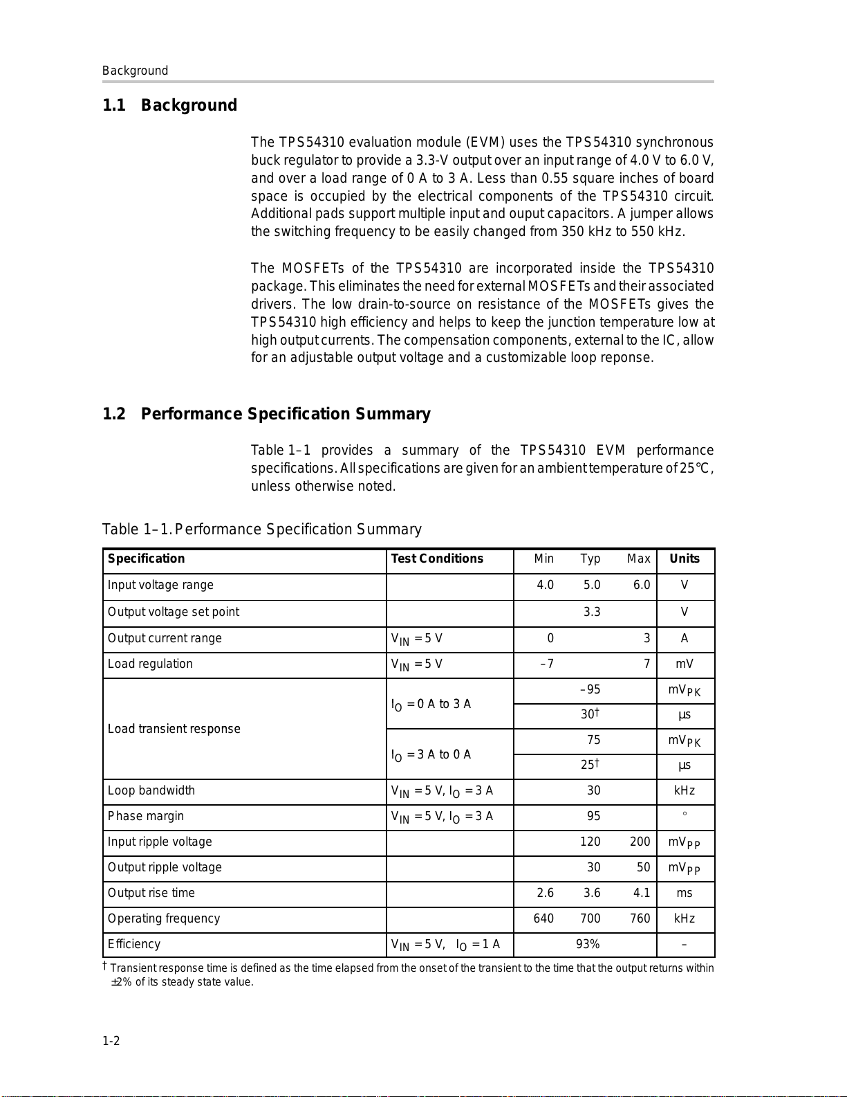
1.2 Performance Specification Summary
Table 1–1 provides a summary of the TPS54310 EVM performance
specifications. All specifications are given for an ambient temperature of 25°C,
unless otherwise noted.
Table 1–1.Performance Specification Summary
Specification Test Conditions Min Typ Max Units
Input voltage range 4.0 5.0 6.0 V
Output voltage set point 3.3 V
Output current range VIN = 5 V 0 3 A
Load regulation VIN = 5 V –7 7 mV
–95 mV
IO = 0 A to 3 A
Load transient response
Loop bandwidth VIN = 5 V, IO = 3 A 30 kHz
Phase margin VIN = 5 V, IO = 3 A 95 _
Input ripple voltage 120 200 mV
Output ripple voltage 30 50 mV
Output rise time 2.6 3.6 4.1 ms
Operating frequency 640 700 760 kHz
p
IO = 3 A to 0 A
†
30
75 mV
†
25
µs
µs
PK
PK
PP
PP
Efficiency VIN = 5 V, IO = 1 A 93% –
†
Transient response time is defined as the time elapsed from the onset of the transient to the time that the output returns within
±2% of its steady state value.
1-2
Page 10
1.3 Modifications
1.3.1 General
The TPS54310 EVM is designed to demonstrate the small amount of board
space taken up by the TPS54310 electrical components. In addition, the EVM
can be used to evaluate different output filters by substituting an alternate
inductor for L1, or by using the optional pads for capacitors C2 and C1 1 (see
Figure 3–1). When changing the output filter, the compensation values must
also be changed to ensure that stability is maintained. The SWIFT Designer
software tool or Texas Instruments application note SL VA109 can be used to
assist in the calculation of compensation components. Both SWIFT Designer
and SLVA109 are available for download at the Texas Instruments web site.
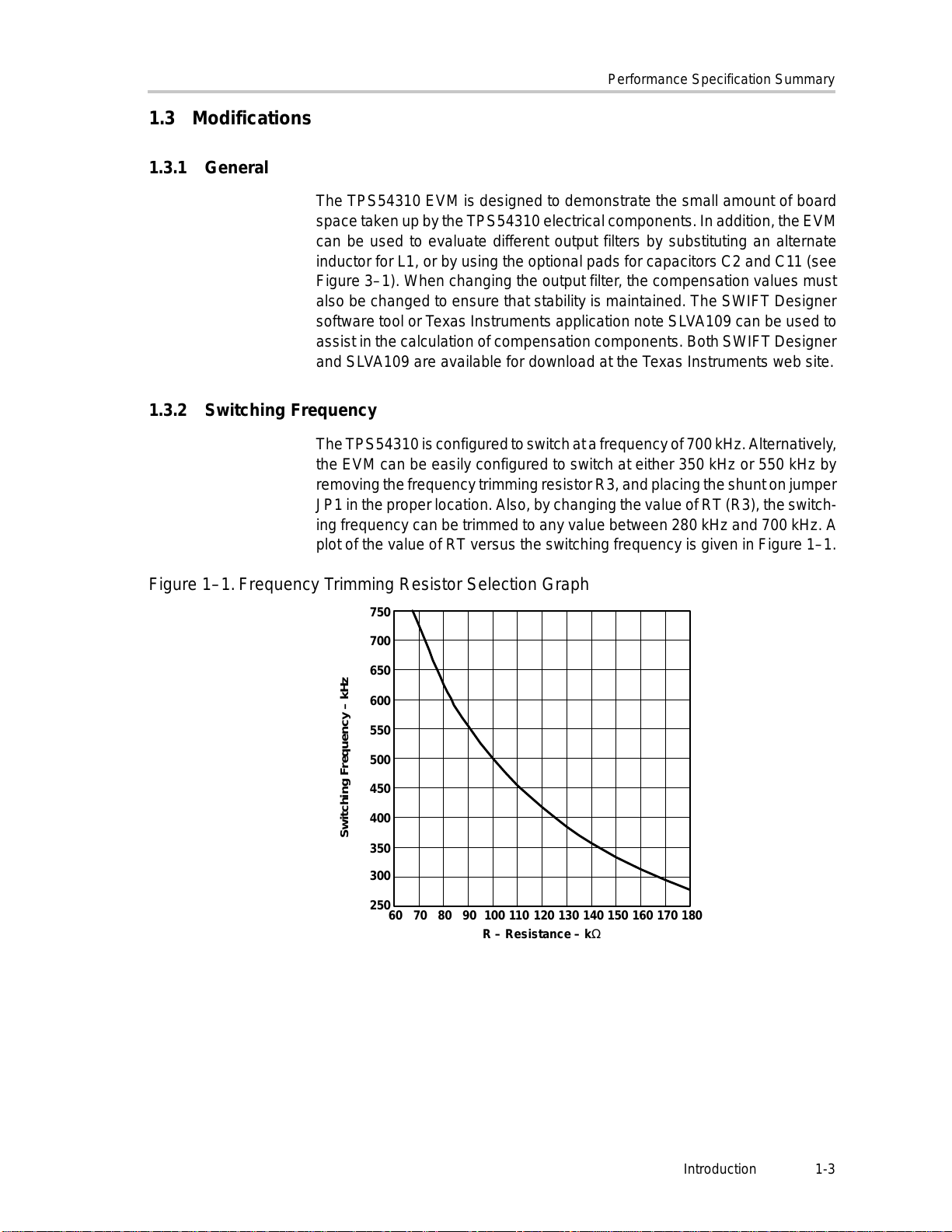
1.3.2 Switching Frequency
The TPS54310 is configured to switch at a frequency of 700 kHz. Alternatively ,
the EVM can be easily configured to switch at either 350 kHz or 550 kHz by
removing the frequency trimming resistor R3, and placing the shunt on jumper
JP1 in the proper location. Also, by changing the value of RT (R3), the switch-
ing frequency can be trimmed to any value between 280 kHz and 700 kHz. A
plot of the value of RT versus the switching frequency is given in Figure 1–1.
Performance Specification Summary
Figure 1–1.Frequency Trimming Resistor Selection Graph
750
700
650
600
550
500
450
400
Switching Frequency – kHz
350
300
250
60 70 80 90 100 110 120 130 140 150 160 170 180
R – Resistance – kΩ
Introduction
1-3
Page 11
Performance Specification Summary
1.3.3 Output Voltage
The output voltage of the TPS54310 EVM can be adjusted to any value down
to 0.9 V by changing only one component value (R4). The value of R4 for a
specific output voltage can be calculated by using equation 1–1. Table 1–2
lists the value of R4 for some common bus voltages.
R4+ 10 kW
Table 1–2.Output Voltage Programming
Output Voltage
(V)
0.9 1000
1.2 28.7
1.5 14.7
1.8 9.76
2.5 5.49
3.3 3.74
1.3.4 Slow Start
The slow start time of the EVM can be modified by changing the value of C1.
Use equation 1–2 to calculate the value of C1 for a specific slow start time. With
C1 open, the slow start time is typically 3.6 ms. The slow start time can not be
made faster than 3.6 ms.
0.891 V
VO–0.891 V
(1–1)
R4
(kΩ)
TSS 5 mA
C
+
1
0.891 V
1.3.5 Improving Transient Response
The feedback compensation components are R2, R4, R5, R6, C4, C5, and C6
(see Figure 4–1), and were selected based on the output of the SWIFT
Designer software tool. This results in a unity gain bandwidth of 30 kHz, and
a phase margin of 95° (see Figure 2–8). The TPS54310 EVM responds to a
3-A load transient within 30 µs using the compensation shown in the
schematic. While this response time is more than sufficient for most
applications, the response time can be made faster by changing the values of
the feedback compensation components. Using the values given by
Table 1–3, the unity gain bandwidth is increased to 75 kHz, and the phase
margin is 72° (see Figure 2–9). With this alternate compensation, the output
voltage remains within a ±2% regulation band during a 3-A load transient (see
Figure 2–7).
(1–2)
1-4
Page 12

Performance Specification Summary
Table 1–3.Alternate Compensation for Improved Transient Response
Reference Designator Component Value
R2 15 kΩ
R4 3.74 kΩ
R5 10 kΩ
R6 1.78 kΩ
C4 33 pF
C5 1000 pF
C6 1500 pF
Introduction
1-5
Page 13

1-6
Page 14

Chapter 2
Test Setup and Results
This chapter describes how to properly connect, setup, and use the TPS54310
EVM. It also presents the test results and covers efficiency, output voltage
regulation, load transients, loop response, output ripple, input ripple, and
start-up.
Topic Page
2.1 Input/Output Connections 2-2. . . . . . . . . . . . . . . . . . . . . . . . . . . . . . . . . . . . .
2.2 Loop Characterization Setup 2-3. . . . . . . . . . . . . . . . . . . . . . . . . . . . . . . . . . .
2.3 Efficiency 2-3. . . . . . . . . . . . . . . . . . . . . . . . . . . . . . . . . . . . . . . . . . . . . . . . . . . .
2.4 Thermal Performance 2-4. . . . . . . . . . . . . . . . . . . . . . . . . . . . . . . . . . . . . . . . .
2.5 Output Voltage Regulation 2-5. . . . . . . . . . . . . . . . . . . . . . . . . . . . . . . . . . . . .
2.6 Load Transients 2-6. . . . . . . . . . . . . . . . . . . . . . . . . . . . . . . . . . . . . . . . . . . . . . .
2.7 Loop Characteristics 2-7. . . . . . . . . . . . . . . . . . . . . . . . . . . . . . . . . . . . . . . . . .
2.8 Output V oltage Ripple 2-8. . . . . . . . . . . . . . . . . . . . . . . . . . . . . . . . . . . . . . . . .
2.9 Input Ripple Voltage 2-9. . . . . . . . . . . . . . . . . . . . . . . . . . . . . . . . . . . . . . . . . . .
2.10 Start-Up 2-10. . . . . . . . . . . . . . . . . . . . . . . . . . . . . . . . . . . . . . . . . . . . . . . . . . . . .
Test Setup and Results
2-1
Page 15

Input/Output Connections
2.1 Input/Output Connections
The TPS54310 EVM has the following four input/output connections: J1 (V
and GND) and J3 (V
is shown in Figure 2–1. Connect a power supply capable of supplying 3 A to
J1 through a pair of 20 AWG wires. Connect the load to J3 through a pair of
20 AWG wires. Minimize wire lengths to reduce losses in the wires. Test point
TP8 provides easy connection for an oscilloscope voltage probe to monitor the
output voltage.
Figure 2–1.Connection Diagram
and GND). A diagram showing the connection points
out
in
2-2
Page 16

2.2 Loop Characterization Setup
The TPS54310 EVM contains a 49.9 Ω resistor (R7) in the feedback path for
use in measuring the loop response. T est points on either side of R7 (TP5 and
TP7) provide connection points for network analyzer signals. By injecting a
small ac signal across R7, the loop gain and phase can be measured from one
side of R7 to the other. Because the value of R7 is small in relation to the value
of R5, it does not significantly affect the output voltage set point of the
regulator.
2.3 Efficiency
The TPS54310 EVM efficiency peaks at around 1 A of load current. At full load
this drops to around 90.5%. Figure 2–2 shows the typical efficiency for a 5-V
input and an ambient temperature of 25
ambient temperatures due to temperature variation in the drain-to-source
resistance of the MOSFETs. The efficiency is also slightly higher at lower
switching frequencies due to the gate and switching losses in the MOSFETs.
The total board losses are shown in Figure 2–3.
Figure 2–2.Measured Efficiency
96
TA = 25°C
VI = 5 V
94
Loop Characterization Setup
°
C. The efficiency is lower at higher
92
90
88
Efficency – %
86
84
82
80
0 0.5 1 1.5 2 2.5 3
IL – Load Current – A
Test Setup and Results
2-3
Page 17

Thermal Performance
Figure 2–3.Measured Board Losses
1.2
1
0.8
0.6
Losses – W
0.4
0.2
0
0 0.5 1 1.5 2 2.5 3
2.4 Thermal Performance
TA = 25°C
VI = 5 V
IL – Load Current – A
The junction temperature is plotted versus the load current with a 5-V input
voltage and a 25°C ambient temperature in Figure 2–4. The low junction-to-
case thermal resistance of the PWP package, along with a good board layout,
helps to keep the junction temperature low at high output currents. With a 5-V
input source and a 3-A load, the junction temperture is approximately 47
Figure 2–4.Measured Junction Temperature at 25°C Ambient
50
TA = 25°C
VI = 5 V
45
C
°
40
35
30
– Junction Temperature –
J
T
25
20
0 0.5 1 1.5 2 2.5 3
IL – Load Current – A
°
C.
2-4
Page 18

2.5 Output Voltage Regulation
The output voltage load regulation, with a 5-V input and a 25°C ambient
temperature, is shown in Figure 2–5. Over the load range of 0 A to 3 A, the
output voltage varies less than 0.2%.
Figure 2–5.Measured Load Regulation
1.01
1.008
1.006
1.004
1.002
1
0.998
– Output Voltage – V
0.996
O
V
(Normalized to 1.5 A Load)
0.994
0.992
Output Voltage Regulation
TA = 25°C
VI = 5 V
0.99
0 0.5 1 1.5 2 2.5 3
IL – Load Current – A
Test Setup and Results
2-5
Page 19

Load Transients
2.6 Load Transients
The TPS54310 EVM response to load transients is shown in Figure 2–6. The
load transient in Figure 2–6 transitions between 0 A and 3 A. The output
voltage deviates approximately –95 mV (–2.9%) and 75 mV (2.3%) from its
average value as a result of these transients. In Figure 2–6, the output voltage
returns to a ±2% regulation band within 30 µs. Using the alternate feedback
compensation described in Section 1.3.5 Improving T ransient Response, the
output voltage deviation can be reduced to –55 mV (–1.7%) and 45 mV (1.4%),
as shown in Figure 2–7. With the alternate compensation, the output voltage
remains within a ±2% regulation band through the duration of the load
transient.
Figure 2–6.Measured Load Transient Response
VI = 5 V
40 µs/div
VO (AC)
50 mV/div
Figure 2–7.Improved Load Transient Response
VI = 5 V
20 µs/div
IO
2 A/div
VO (AC)
50 mV/div
IO
2 A/div
2-6
Page 20

2.7 Loop Characteristics
The loop gain and phase for a 5.0-V input and a 3.0-A load is shown in
Figure 2–8. The loop crossover frequency is approximately 30 kHz, and the
phase margin is approximately 75
the alternate compensation described in Section 1.3.5 Improving Transient
Response. With the alternate feedback compensation, the loop crossover
frequency is approximately 75 kHz, and the phase margin is approximately
72°.
Figure 2–8.Improved Loop Gain and Phase
Loop Characteristics
°
. Figure 2–9 shows the loop response using
60
TA = 25°C
VI = 5 V
40
20
Gain – dB
0
–20
100 1 k 10 k 100 k 1 M
Phase
Gain
f – Frequency – Hz
Figure 2–9.Measured Loop Gain and Phase for Alternate Compensation
60
TA = 25°C
VI = 5 V
135
90
45
Phase – Degrees
0
–45
135
Phase
40
20
Gain – dB
0
–20
100 1 k 10 k 100 k 1 M
Gain
f – Frequency – Hz
Test Setup and Results
90
45
Phase – Degrees
0
–45
2-7
Page 21

Output Voltage Ripple
2.8 Output Voltage Ripple
The output ripple voltage is plotted in Figure 2–10 with an input voltage of 5.0 V
and a load current of 3 A. The TPS54310 EVM has a typical output voltage
ripple of less than 33 mV
ripple voltage is higher. The output ripple voltage can be decreased by using
a larger inductor, or by reducing the equivalent series resistance of the output
capacitor. Changing either of these components requires the feedback
compensation to be redesigned.
Figure 2–10. Measured Output Voltage Ripple
VI = 5 V
IO = 3 A
400 ns/div
pp
. If the switching frequency is reduced, the output
VO (AC)
10 mV/div
2-8
Page 22

2.9 Input Ripple Voltage
The input ripple voltage for a 3-A load is shown in Figure 2–1 1. With an input
voltage of 5.0 V, the input ripple is approximately 120 mV
voltage can be made lower by adding capacitance to the input.
Figure 2–11. Measured Input Voltage Ripple
VI = 5 V
IO = 3 A
400 ns/div
Input Ripple Voltage
. The input ripple
pp
VI (AC)
50 mV/div
Test Setup and Results
2-9
Page 23

Start-Up
2.10 Start-Up
Figure 2–12 shows the start-up voltage waveform of the TPS54310 EVM with
C1 left open. The input voltage is displayed on channel 3, the output voltage
on channel 1, and the power good signal on channel 2. Once the input voltage
rises above the 2.9-V start-up threshold, the output voltage begins to rise
linearly to 3.3 V in 3.6 ms. When the output voltage has reached its final value,
the open-drain power good signal rises to a high state. The start-up time can
be extended by using an external slow-start capacitor, C1. To program a
specific slow start time, see Section 1.3.4 Slow Start.
The shorting jumper on J2 should not be used to enable the EVM, as this may
cause excessive voltage transients on the SS/ENA pin. Use an external
enable signal instead of the J2 jumper.
Figure 2–12. Measured Start-Up Waveforms
VI (2 V/div)
3
1
2
VO (2 V/div)
V
(PWRGD)
(5 V/div)
1 ms/div
2-10
Page 24
Chapter 3
Board Layout
This chapter provides a description of the TPS54310 EVM board layout and
layer illustrations.
Topic Page
3.1 Layout 3-2. . . . . . . . . . . . . . . . . . . . . . . . . . . . . . . . . . . . . . . . . . . . . . . . . . . . . . .
Board Layout
3-1
Page 25

Layout
3.1 Layout
The top-side layer for the TPS54310 EVM is shown in Figure 3–1. The input
capacitors (C8 and C9), bias decoupling capacitor (C3), and bootstrap
capacitor (C7), are all located as close to the IC as possible. In addition, the
feedback compensation components are also kept close to the IC. The
compensation circuit ties to the output voltage at the point of regulation (TP7).
The TPS54310 EVM PWB consists of two layers of 1.5 oz. copper. The bottom
half of the top layer is used as a power ground plane, while the bottom layer
is used as a quiet (analog) ground plane. The two ground planes tie together
at U1 to reduce the noise injected between the two IC ground connections. A
total of 10 vias are used to tie the thermal land area under the TPS54310
device to the thermal plane on the backside of the board.
Figure 3–1.Top Side Assembly
3-2
Page 26

Figure 3–2.Bottom Side Assembly
Layout
Board Layout
3-3
Page 27

Layout
Figure 3–3.Top Side Layout
3-4
Page 28

Figure 3–4.Bottom Side Layout
Layout
Board Layout
3-5
Page 29

3-6
Page 30

Chapter 4
Schematic and Bill of Materials
The EVM schematic and bill of materials are presented in this chapter.
Topic Page
4.1 Schematic 4-2. . . . . . . . . . . . . . . . . . . . . . . . . . . . . . . . . . . . . . . . . . . . . . . . . . . .
4.2 Bill of Materials 4-3. . . . . . . . . . . . . . . . . . . . . . . . . . . . . . . . . . . . . . . . . . . . . . .
Schematic and Bill of Materials
4-1
Page 31

Schematic
4.1 Schematic
Figure 4–1.TPS54310 EVM Schematic
VIN
GND
SYNCH
SS/ENA
GND
PWRGD
VIN
TP2
R1
10 kΩ
TP1
C2
TP3
C3
0.1 µF
JP1
C4
100 pF
R3
C5
3000 pF
R2
3.74 kΩ
71.5 kΩ
R4
3.74 kΩ
20
RT
19
SYNCH
18
SS/ENA
17
VBIAS
4
PWRGD
3
COMP/NC
2
VSENSE
BOOT
PGND
1
PGND
ANAGND
PGND
PwrPad
C6
2700 pFR6732 Ω
R5
10 kΩ
C8
TP5
10 µF
L1
1.2 µH
+
C9
180 µF
4 V
TP6
TP7
C10
+
C11
1000 pF
J3
1
V
OUT
2
GND
TP8
R7
16
VIN
15
TP4
VIN
14
VIN
10
PH
9
PH
8
PH
7
PH
6
PH
C7
5
13
0.047 pF
12
11
49.9 Ω
+
C1
VIN
J1
2
1
J2
Optinal
4-2
Page 32

Bill of Materials
4.2 Bill of Materials
Table 4–1.TPS54310 EVM BIll of Materials
Count Ref Des Description Size MFR Part Number
1 C1 Open 603
1 C11 Capacitor, ceramic, 1000 pF, 25 V , X7R, 10% 603 Vishay VJ0603Y102KXXAT
2 C2, C10 Open 7343 (D)
1 C3 Capacitor, ceramic, 0.1 µF, 25 V, X7R, 10% 603 Vishay VJ0603Y104KXXMT
1 C4 Capacitor, ceramic, 100 pF, 50 V, C0G, 5% 603 Vishay VJ0603A101KXAAC
1 C5 Capacitor, ceramic, 3900 pF, 50 V, X7R, 10% 603 Vishay VJ0603Y392KXAAB00
1 C6 Capacitor, Ceramic, 2700 pF, 50 V, X7R, 10% 603 Vishay VJ0603Y272KXAAB00
1 C7 Capacitor, ceramic, 0.047 µF, 25 V, X7R, 10% 603 Vishay VJ0603Y473KXXAB00
1 C8 Capacitor, ceramic, 10 µF, 10 V, X5R, 20% 1210 Panasonic ECJ–4YB1A106K
1 C9 Capacitor, spec polymer, 180 µF, 4 V, 20% 7343 Panasonic EEF–UEG181R
2 J1, J3 Terminal block, 2 pin, 6 A, 3,5 mm 0.27 x 0.25 OST ED1514
1 J2 Header, 4 pin, 100 mil spacing, (36-pin strip) 0.100 x 4 Sullins PTC36SAAN
1 JP1 Header, 3 pin, 100 mil spacing, (36-pin strip) 0.100 x 3 Sullins PTC36SAAN
1 L1 Inductor, SMT, 1.2 µH, 4.4 A, 17–mΩ Coilcraft DO1813P–122HC
1 R1 Resistor, chip, 10 kΩ, 1/16 W, 1% 603 Vishay CRCW060310K0FKSF
1 R2 Resistor, chip, 3.74 kΩ, 1/16 W, 1% 603 Vishay CRCW06033K74FKTA
1 R3 Resistor, chip, 71.5 kΩ, 1/16 W, 1% 603 Vishay CRCW060371K5FKTA
1 R4 Resistor, chip, 3.74 kΩ, 1/16 W, 0.1% 603 Vishay TNPW06033741BT9RT
1 R5 Resistor, chip, 10 kΩ, 1/16 W, 0.1% 603 Vishay TNPW060310K0BETAR2
1 R6 Resistor, chip, 732 Ω, 1/16 W, 1% 603 Vishay CRCW0603732RFKTA
1 R7 Resistor, chip, 49.9 Ω, 1/16 W, 1% 603 Vishay CRCW060349R9FKSF
5 TP1,
TP3–TP5,
TP7
2 TP2, TP6 Test point, black, 1 mm 0.038” Farnell 240–333
1 TP8 Adaptor, 3,5 mm probe clip ( or 131–5031–00) 0.200” Tektronix 131–4244–00
1 U1 IC, SWIFT power controller, Adj V, 3 A PWP20 TI TPS54310PWP
1 –– PCB, 3 In x 3 In x 0.062 In Any SLVP201
2 –– Shunt, 100 mil, black 0.100 3M 929950–00
Test point, red, 1 mm 0.038” Farnell 240–345
Schematic and Bill of Materials
4-3
Page 33

4-4
Page 34

EN
This Datasheet is presented by
the manufacturer
DE
Dieses Datenblatt wird vom
Hersteller bereitgestellt
FR
Cette fiche technique est
présentée par le fabricant
EN - For pricing and availability in your local country please visit one of the below links:
DE - Informationen zu Preisen und Verfügbarkeit in Ihrem Land erhalten Sie über die unten aufgeführten Links:
FR - Pour connaître les tarifs et la disponibilité dans votre pays, cliquez sur l'un des liens suivants:
TPS54310EVM
Powered by TCPDF (www.tcpdf.org)
 Loading...