

Page 1
0
10
20
30
40
50
60
70
80
100
0 0.5 1.0 1.5 2.0
I - Output Current - A
O
Efficiency - %
2.5 3.0
90
VIN=12V
VOUT=3.3V
fsw=300kHz
PH
VIN
GND
BOOT
VSENSE
COMP
TPS54240
EN
RT /CLK
SS /TR
PWRGD
TPS54240
www.ti.com
SLVSAA6 –APRIL 2010
3.5V to 42V STEP DOWN SWIFT™ DC/DC CONVERTER WITH ECO-MODE™
Check for Samples: TPS54240
1
FEATURES
2
• 3.5V to 42V Input Voltage Range
• 200-mΩ High-Side MOSFET • Supported by SwitcherPro™ Software Tool
• High Efficiency at Light Loads with a Pulse
Skipping Eco-Mode™
• 138mA Operating Quiescent Current
• 1.3mA Shutdown Current
• 100kHz to 2.5MHz Switching Frequency
• Synchronizes to External Clock
• Adjustable Slow Start/Sequencing
• UV and OV Power Good Output
• Adjustable UVLO Voltage and Hysteresis
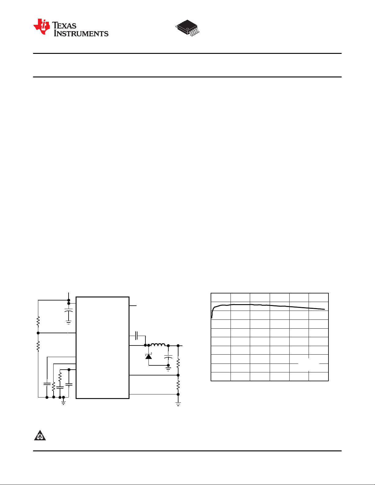
DESCRIPTION
The TPS54240 device is a 42V, 2.5A, step down regulator with an integrated high side MOSFET. Current mode
control provides simple external compensation and flexible component selection. A low ripple pulse skip mode
reduces the no load, regulated output supply current to 138mA. Using the enable pin, shutdown supply current is
reduced to 1.3mA, when the enable pin is low.
Under voltage lockout is internally set at 2.5V, but can be increased using the enable pin. The output voltage
startup ramp is controlled by the slow start pin that can also be configured for sequencing/tracking. An open
drain power good signal indicates the output is within 94% to 107% of its nominal voltage.
A wide switching frequency range allows efficiency and external component size to be optimized. Frequency fold
back and thermal shutdown protects the part during an overload condition.
The TPS54240 is available in 10 pin thermally enhanced MSOP Power Pad™ package.
SIMPLIFIED SCHEMATIC EFFICIENCY vs LOAD CURRENT
• 0.8-V Internal Voltage Reference
• MSOP10 Package With PowerPAD™
(http://focus.ti.com/docs/toolsw/folders/print/s
witcherpro.html)
• For SWIFT™ Documentation, See the TI
Website at http://www.ti.com/swift
APPLICATIONS
• 12-V and 24-V Industrial and Commercial Low
Power Systems
• GSM, GPRS Modules in Fleet Management,
E-Meters, and Security Systems
1
2Eco-Mode, PowerPAD, SwitcherPro, SWIFT are trademarks of Texas Instruments.
PRODUCTION DATA information is current as of publication date.
Products conform to specifications per the terms of the Texas
Instruments standard warranty. Production processing does not
necessarily include testing of all parameters.
Please be aware that an important notice concerning availability, standard warranty, and use in critical applications of Texas
Instruments semiconductor products and disclaimers thereto appears at the end of this data sheet.
Copyright © 2010, Texas Instruments Incorporated
Page 2
TPS54240
SLVSAA6 –APRIL 2010
This integrated circuit can be damaged by ESD. Texas Instruments recommends that all integrated circuits be handled with
appropriate precautions. Failure to observe proper handling and installation procedures can cause damage.
ESD damage can range from subtle performance degradation to complete device failure. Precision integrated circuits may be more
susceptible to damage because very small parametric changes could cause the device not to meet its published specifications.
Table 1. ORDERING INFORMATION
T
J
–40°C to 150°C 10 Pin MSOP TPS54240DGQ
(1) For the most current package and ordering information see the Package Option Addendum at the end
of this document, or see the TI website at www.ti.com.
(2) The DGQ package is also available taped and reeled. Add an R suffix to the device type (i.e.,
TPS54240DGQR).
ABSOLUTE MAXIMUM RATINGS
(1)
(1)
PACKAGE PART NUMBER
(2)
www.ti.com
Over operating temperature range (unless otherwise noted).
VALUE UNIT
VIN –0.3 to 47
EN –0.3 to 5
BOOT 55
Input voltage V
Output voltage PH –0.6 to 47 V
Voltage difference PAD to GND ±200 mV
Source current VSENSE 10 mA
Sink current
Electrostatic discharge (HBM) QSS 009-105 (JESD22-A114A) 2 kV
Electrostatic discharge (CDM) QSS 009-147 (JESD22-C101B.01) 500 V
Operating junction temperature –40 to 150 °C
Storage temperature –65 to 150 °C
(1) Stresses beyond those listed under absolute maximum ratings may cause permanent damage to the device. These are stress ratings
only and functional operation of the device at these or any other conditions beyond those indicated under recommended operating
conditions is not implied. Exposure to absolute-maximum-rated conditions for extended periods may affect device reliability.
VSENSE –0.3 to 3
COMP –0.3 to 3
PWRGD –0.3 to 6
SS/TR –0.3 to 3
RT/CLK –0.3 to 3.6
BOOT-PH 8
PH, 10-ns Transient –2 to 47
EN 100 mA
BOOT 100 mA
PH Current Limit A
RT/CLK 100 mA
VIN Current Limit A
COMP 100 mA
PWRGD 10 mA
SS/TR 200 mA
2 Submit Documentation Feedback Copyright © 2010, Texas Instruments Incorporated
Product Folder Link(s): TPS54240
Page 3
TPS54240
www.ti.com
PACKAGE DISSIPATION RATINGS
PACKAGE
MSOP 57 °C/W
(1) Test board conditions:
A. 3 inches × 3 inches, 2 layers, thickness: 0.062 inch
B. 2-ounce copper traces located on the top and bottom of the PCB
C. 6 (13 mil diameters) THERMAL VIAS LOCATED UNDER THE DEVICE PACKAGE
ELECTRICAL CHARACTERISTICS
TJ= –40°C to 150°C, VIN = 3.5 to 42V (unless otherwise noted)
PARAMETER TEST CONDITIONS MIN TYP MAX UNIT
SUPPLY VOLTAGE (VIN PIN)
Operating input voltage 3.5 42 V
Internal undervoltage lockout
threshold
Shutdown supply current EN = 0 V, 25°C, 3.5 V ≤ VIN ≤ 42 V 1.3 4
Operating : nonswitching supply
current
ENABLE AND UVLO (EN PIN)
Enable threshold voltage No voltage hysteresis, rising and falling, 25°C 1.15 1.25 1.36 V
Input current mA
Hysteresis current –2.9 mA
VOLTAGE REFERENCE
Voltage reference V
HIGH-SIDE MOSFET
On-resistance mΩ
ERROR AMPLIFIER
Input current 50 nA
Error amplifier transconductance (gM) –2 mA < I
Error amplifier transconductance (gM)
during slow start
Error amplifier dc gain V
Error amplifier bandwidth 2700 kHz
Error amplifier source/sink V
COMP to switch current
transconductance
CURRENT LIMIT
Current limit threshold VIN = 12 V, TJ= 25°C 3.5 6.1 A
THERMAL SHUTDOWN
Thermal shutdown 182 °C
No voltage hysteresis, rising and falling 2.5 V
VSENSE = 0.83 V, VIN = 12 V, 25°C 138 200
Enable threshold +50 mV –3.8
Enable threshold –50 mV –0.9
TJ= 25°C 0.792 0.8 0.808
VIN = 3.5 V, BOOT-PH = 3 V 300
VIN = 12 V, BOOT-PH = 6 V 200 410
< 2 mA, V
COMP
–2 mA < I
V
VSENSE
VSENSE
(COMP)
< 2 mA, V
COMP
= 0.4 V
= 0.8 V 10,000 V/V
= 1 V, 100 mV overdrive ±27 mA
SLVSAA6 –APRIL 2010
(1)
THERMAL IMPEDANCE
JUNCTION TO AMBIENT
0.784 0.8 0.816
= 1 V 310 mMhos
COMP
= 1 V,
COMP
70 mMhos
10.5 A/V
mA
Copyright © 2010, Texas Instruments Incorporated Submit Documentation Feedback 3
Product Folder Link(s): TPS54240
Page 4
TPS54240
SLVSAA6 –APRIL 2010
ELECTRICAL CHARACTERISTICS (continued)
TJ= –40°C to 150°C, VIN = 3.5 to 42V (unless otherwise noted)
PARAMETER TEST CONDITIONS MIN TYP MAX UNIT
TIMING RESISTOR AND EXTERNAL CLOCK (RT/CLK PIN)
Switching Frequency Range using
RT mode
f
SW
SLOW START AND TRACKING (SS/TR)
POWER GOOD (PWRGD PIN)
V
VSENSE
Switching frequency RT= 200 kΩ 450 581 720 kHz
Switching Frequency Range using
CLK mode
Minimum CLK input pulse width 40 ns
RT/CLK high threshold 1.9 2.2 V
RT/CLK low threshold 0.5 0.7 V
RT/CLK falling edge to PH rising
edge delay
PLL lock in time Measured at 500 kHz 100 ms
Charge current V
SS/TR-to-VSENSE matching V
SS/TR-to-reference crossover 98% nominal 1.15 V
SS/TR discharge current (overload) VSENSE = 0 V, V(SS/TR) = 0.4 V 382 mA
SS/TR discharge voltage VSENSE = 0 V 54 mV
VSENSE threshold
Hysteresis VSENSE falling 2%
Output high leakage VSENSE = VREF, V(PWRGD) = 5.5 V, 25°C 10 nA
On resistance I(PWRGD) = 3 mA, VSENSE < 0.79 V 50 Ω
Minimum VIN for defined output V(PWRGD) < 0.5 V, II(PWRGD) = 100 mA 0.95 1.5 V
Measured at 500 kHz with RT resistor in series 60 ns
= 0.4 V 2 mA
SS/TR
= 0.4 V 45 mV
SS/TR
VSENSE falling 92%
VSENSE rising 94%
VSENSE rising 109%
VSENSE falling 107%
www.ti.com
100 2500 kHz
300 2200 kHz
4 Submit Documentation Feedback Copyright © 2010, Texas Instruments Incorporated
Product Folder Link(s): TPS54240
Page 5
1
2
3
4
5
6
7
9
8
10
Thermal
Pad
(11)
BOOT
VIN
EN
PH
GND
COMP
VSENSE
PWRGD
SS/TR
RT/CLK
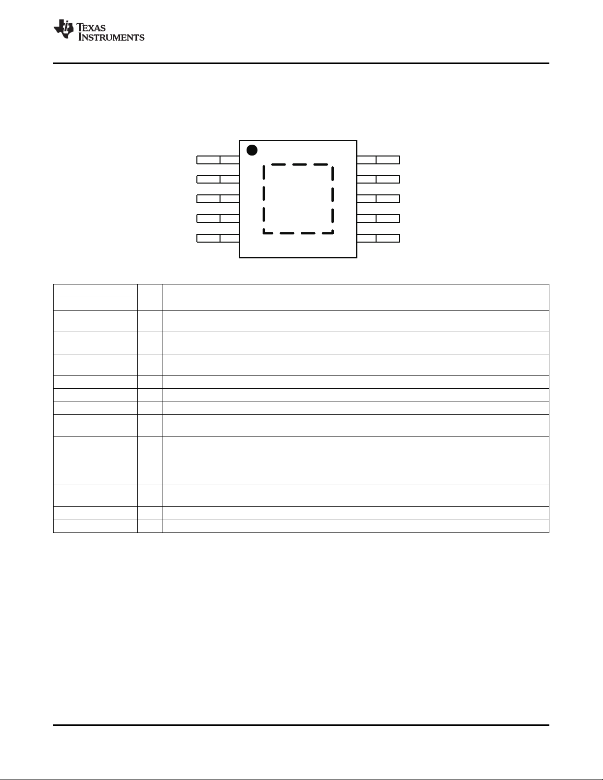
MSOP10
(TOP VIEW)
TPS54240
www.ti.com
SLVSAA6 –APRIL 2010
DEVICE INFORMATION
PIN CONFIGURATION
PIN FUNCTIONS
PIN
NAME NO.
BOOT 1 O
COMP 8 O
EN 3 I
GND 9 – Ground
PH 10 I The source of the internal high-side power MOSFET.
POWERPAD 11 – GND pin must be electrically connected to the exposed pad on the printed circuit board for proper operation.
PWRGD 6 O
RT/CLK 5 I a mode change occurs and the pin becomes a synchronization input. The internal amplifier is disabled and
SS/TR 4 I
VIN 2 I Input supply voltage, 3.5 V to 42 V.
VSENSE 7 I Inverting node of the transconductance ( gm) error amplifier.
I/O DESCRIPTION
A bootstrap capacitor is required between BOOT and PH. If the voltage on this capacitor is below the
minimum required by the output device, the output is forced to switch off until the capacitor is refreshed.
Error amplifier output, and input to the output switch current comparator. Connect frequency compensation
components to this pin.
Enable pin, internal pull-up current source. Pull below 1.2V to disable. Float to enable. Adjust the input
undervoltage lockout with two resistors.
An open drain output, asserts low if output voltage is low due to thermal shutdown, dropout, over-voltage or
EN shut down.
Resistor Timing and External Clock. An internal amplifier holds this pin at a fixed voltage when using an
external resistor to ground to set the switching frequency. If the pin is pulled above the PLL upper threshold,
the pin is a high impedance clock input to the internal PLL. If clocking edges stop, the internal amplifier is
re-enabled and the mode returns to a resistor set function.
Slow-start and Tracking. An external capacitor connected to this pin sets the output rise time. Since the
voltage on this pin overrides the internal reference, it can be used for tracking and sequencing.
Copyright © 2010, Texas Instruments Incorporated Submit Documentation Feedback 5
Product Folder Link(s): TPS54240
Page 6
ERROR
AMPLIFIER
Boot
Charge
Boot
UVLO
UVLO
Current
Sense
Oscillator
withPLL
Frequency
Shift
Logic
And
PWMLatch
Slope
Compensation
PWM
Comparator
Minimum
Clamp
Pulse
Skip
Maximum
Clamp
Voltage
Reference
Overload
Recovery
VSENSE
SS/TR
COMP
RT/CLK
PH
BOOT
VIN
Thermal
Shutdown
EN
Enable
Comparator
Shutdown
Logic
Shutdown
Enable
Threshold
TPS54240 BlockDiagram
Logic
Shutdown
PWRGD
Shutdown
OV
GND
POWERPAD
7
4
8
5
9
11
10
1
2
3
6
UV
TPS54240
SLVSAA6 –APRIL 2010
FUNCTIONAL BLOCK DIAGRAM
www.ti.com
6 Submit Documentation Feedback Copyright © 2010, Texas Instruments Incorporated
Product Folder Link(s): TPS54240
Page 7
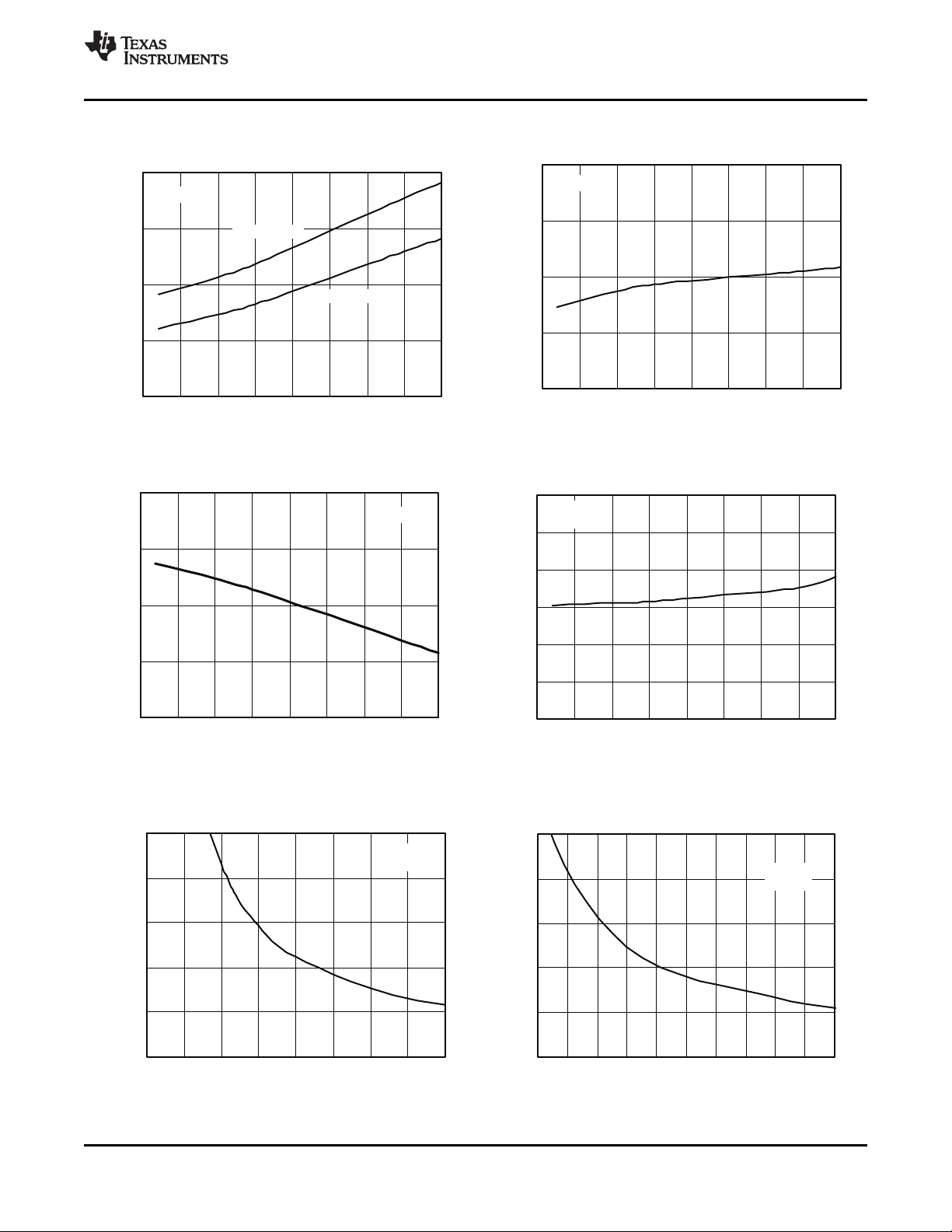
0.784
0.792
0.800
0.808
0.816
-50 -25 0 25 50 75 100 125 150
V -VoltageReference-V
ref
T -JunctionTemperature-°C
J
V =12V
I
0
125
250
375
500
-50 -25 0 25 50 75 100 125 150
T -JunctionTemperature-°C
J
RDSON-StaticDrain-SourceOn-StateResistance-mW
BOOT-PH=3V
BOOT-PH=6V
V =12V
I
550
570
580
590
600
610
-50 -25 0 25 50 75 100 125 150
f -SwitchingFrequency-kHz
s
560
T -JunctionTemperature-°C
J
V =12V,
RT =200kIW
5.0
5.5
6.0
7.0
-50 -25 0 25 50 75 100 125 150
SwitchCurrent- A
T -JunctionTemperature-°C
J
6.5
V =12V
I
0
500
1000
1500
2000
2500
0 25 50 75 100 125 150 175 200
RT/CLK-Resistance-kW
f -SwitchingFrequency-kHz
s
V =12V,
T =25°C
I
J
0
100
200
300
400
500
200 300 400 500 600 700 800 900 1000 1100
RT/CLK-Resistance-kW
f -SwitchingFrequency-kHz
s
1200
V =12V,
T =25°C
I
J
TPS54240
www.ti.com
SLVSAA6 –APRIL 2010
TYPICAL CHARACTERISTICS
ON RESISTANCE vs JUNCTION TEMPERATURE VOLTAGE REFERENCE vs JUNCTION TEMPERATURE
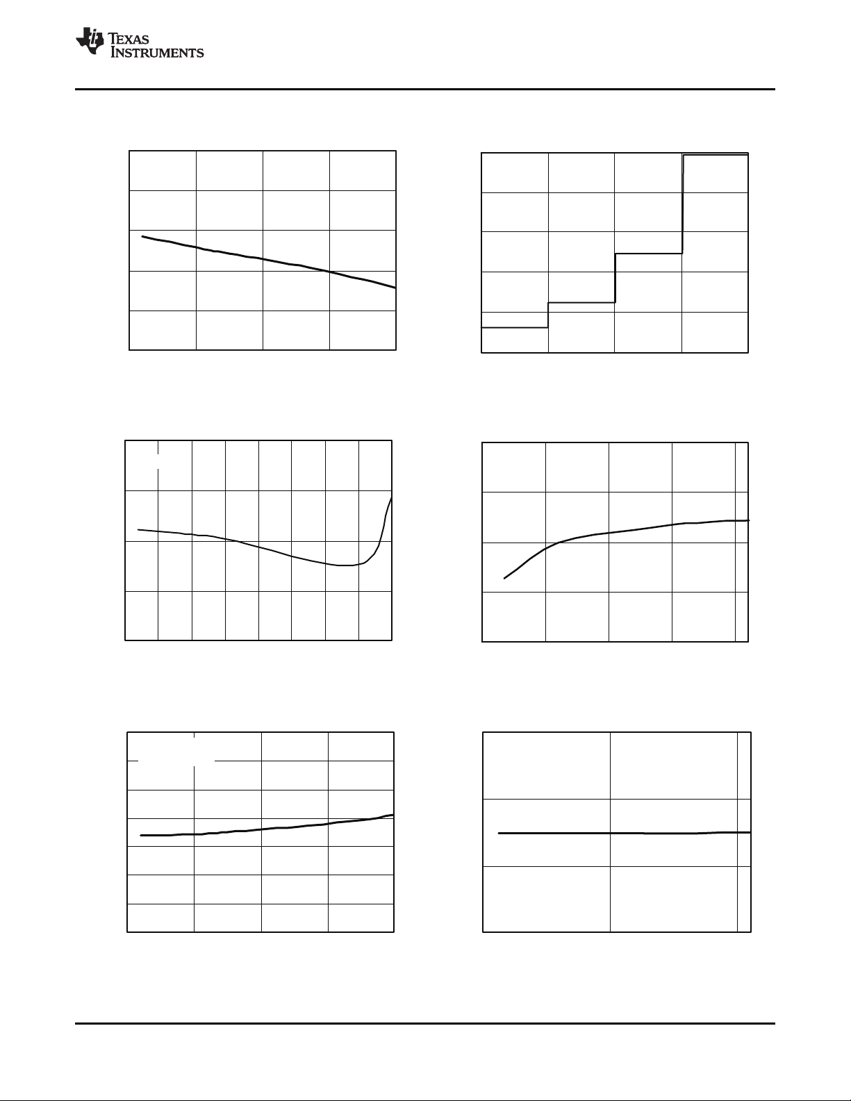
Figure 1. Figure 2.
SWITCH CURRENT LIMIT vs JUNCTION TEMPERATURE SWITCHING FREQUENCY vs JUNCTION TEMPERATURE
Figure 3. Figure 4.
SWITCHING FREQUENCY vs RT/CLK RESISTANCE HIGH SWITCHING FREQUENCY vs RT/CLK RESISTANCE LOW
FREQUENCY RANGE FREQUENCY RANGE
Copyright © 2010, Texas Instruments Incorporated Submit Documentation Feedback 7
Figure 5. Figure 6.
Product Folder Link(s): TPS54240
Page 8
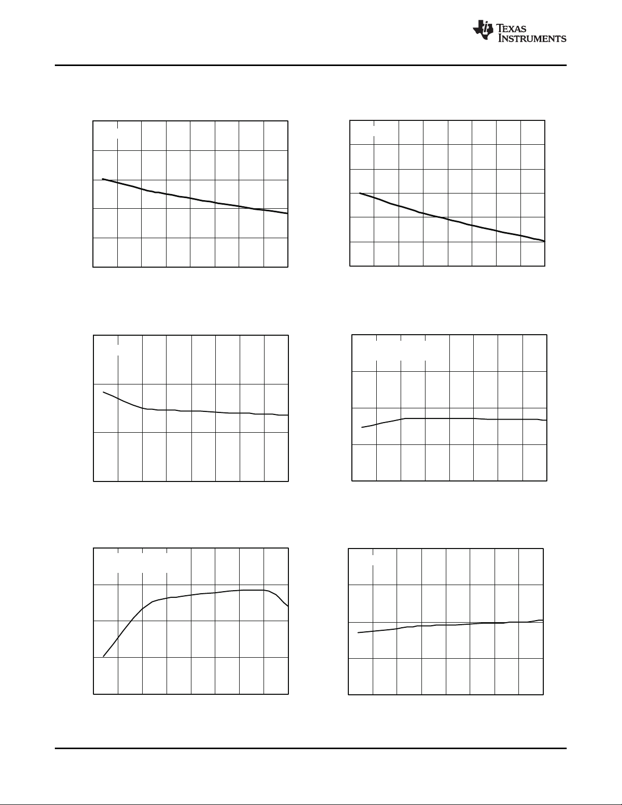
20
60
100
120
-50 -25 0 25 50 75 100 125 150
gm- A/Vm
T -JunctionTemperature-°C
J
V =12V
I
40
80
200
250
300
350
400
500
-50 -25 0 25 50 75 100 125 150
gm- A/Vm
T -JunctionTemperature-°C
J
V =12V
I
450
1.10
1.20
1.30
1.40
-50
-25 0 25 50
75
100
125
150
EN-Threshold-V
T -JunctionTemperature-°C
J
V =12V
I
-4.25
-4
-3.75
-3.5
-3.25
-50 -25 0 25 50 75 100 125 150
I - A
(EN)
m
T -JunctionTemperature-°C
J
V =12V,
V = Threshold+50mV
I
I(EN)
-1
-0.95
-0.9
-0.85
-0.8
-50 -25
0
25
50 75 100
125
150
I - A
(EN)
m
T -JunctionTemperature-°C
J
V =12V,
V = Threshold-50mV
I
I(EN)
-3
-2.5
-2
-1.5
-1
-50 -25 0 25 50 75 100 125 150
I - A
(SS/TR)
m
T -JunctionTemperature-°C
J
V =12V
I
TPS54240
SLVSAA6 –APRIL 2010
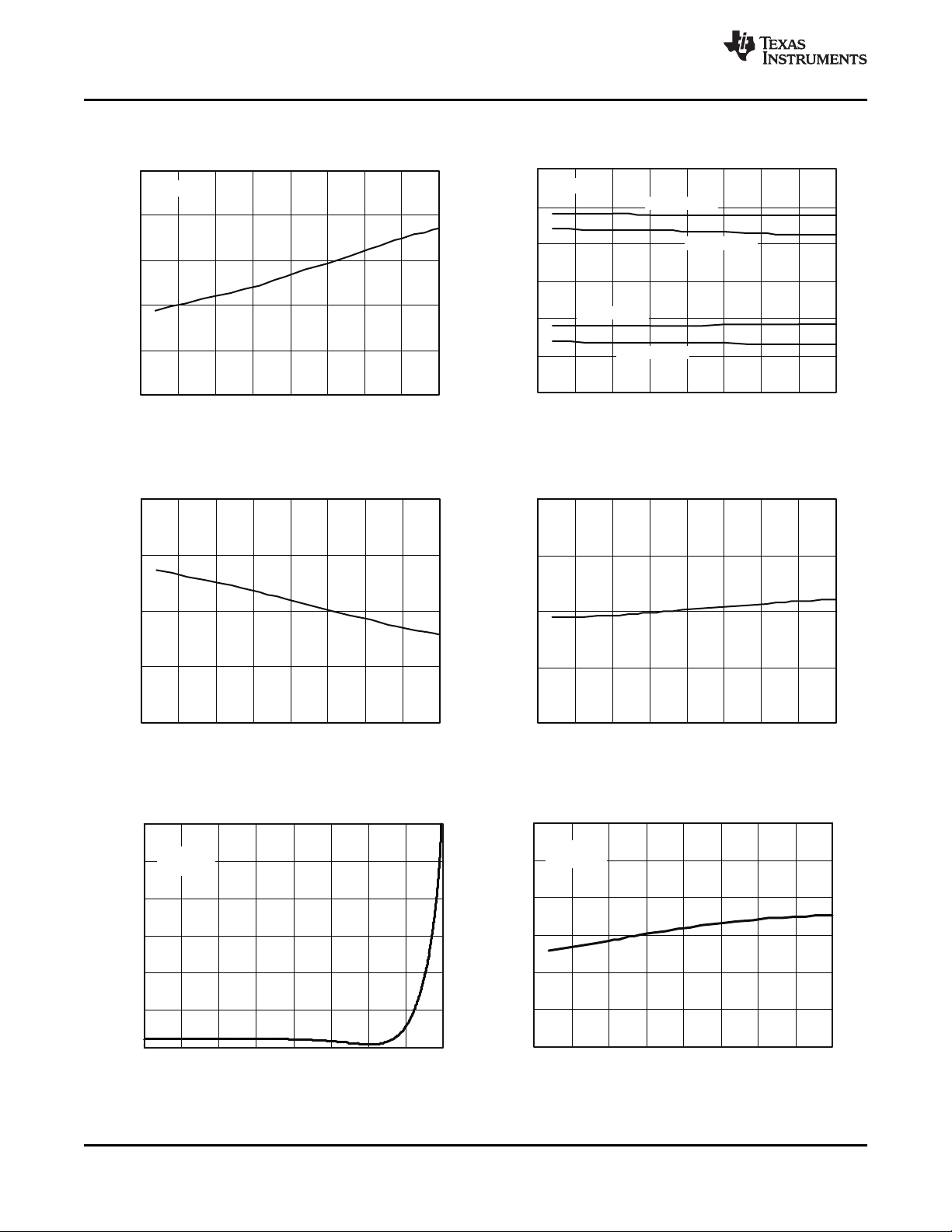
TYPICAL CHARACTERISTICS (continued)
EA TRANSCONDUCTANCE DURING SLOW START vs
JUNCTION TEMPERATURE EA TRANSCONDUCTANCE vs JUNCTION TEMPERATURE
Figure 7. Figure 8.
EN PIN VOLTAGE vs JUNCTION TEMPERATURE EN PIN CURRENT vs JUNCTION TEMPERATURE
www.ti.com
Figure 9. Figure 10.
EN PIN CURRENT vs JUNCTION TEMPERATURE SS/TR CHARGE CURRENT vs JUNCTION TEMPERATURE
8 Submit Documentation Feedback Copyright © 2010, Texas Instruments Incorporated
Figure 11. Figure 12.
Product Folder Link(s): TPS54240
Page 9
200
275
350
425
575
-50 0 50 100 150
I - A
I(SS/TR)
m
T -JunctionTemperature-°C
J
V =12V
I
500
0
20
40
60
80
100
0 0.2 0.4 0.6 0.8
V -V
SENSE
V =12V,
T =25°C
I
J
%ofNominalf
sw
0
0.5
1
1.5
2
-50 -25 0 25 50 75 100 125 150
I - A
(VIN)
m
T -JunctionTemperature-°C
J
V =12V
I
0
0.5
1
1.5
2
0 10 20 30 40
V -InputVoltage-V
I
I - A
(VIN)
m
T =25°C
J
70
110
130
150
170
210
-50 0 50 100 150
I - A
(VIN)
m
T -JunctionTemperature-°C
J
V =12V,
V =0.83V
I
I(VSENSE)
90
190
110
130
150
170
0 20
40
I - A
(VIN)
m
V -InputVoltage-V
I
T =25 C,
V =0.83V
J
I(VSENSE)
o
TPS54240
www.ti.com
SLVSAA6 –APRIL 2010
TYPICAL CHARACTERISTICS (continued)
SS/TR DISCHARGE CURRENT vs JUNCTION TEMPERATURE SWITCHING FREQUENCY vs VSENSE
Figure 13. Figure 14.
SHUTDOWN SUPPLY CURRENT vs JUNCTION TEMPERATURE SHUTDOWN SUPPLY CURRENT vs INPUT VOLTAGE (Vin)
Figure 15. Figure 16.
VIN SUPPLY CURRENT vs JUNCTION TEMPERATURE VIN SUPPLY CURRENT vs INPUT VOLTAGE
Copyright © 2010, Texas Instruments Incorporated Submit Documentation Feedback 9
Figure 17. Figure 18.
Product Folder Link(s): TPS54240
Page 10
85
90
95
100
105
110
115
-50 -25 0 25 50 75 100 125 150
PWRGDThreshold-%ofV
ref
VSENSEFalling
VSENSERising
VSENSEFalling
VSENSERising
V =12V
I
T -JunctionTemperature-°C
J
0
20
40
60
80
100
-50
-25
0 25
50
75
100
125
150
RDSON- W
T -JunctionTemperature-°C
J
V =12V
I
2
2.25
2.50
2.75
3
-50 -25 0 25 50 75 100 125 150
V -V
I(VIN)
T -JunctionTemperature-°C
J
1.5
1.8
2
2.3
2.5
-50 -25 0 25 50 75 100 125 150
V -V
I(BOOT-PH)
T -JunctionTemperature-°C
J
0
100
200
300
400
500
0 100 200 300 400 500 600 700 800
VSENSE-mV
Offset-mV
600
V =12V,
I
T =25 C
J
o
0
10
20
30
40
50
60
-50 -25 0 25 50 75 100 125 150
Offset-mV
T -JunctionTemperature-°C
J
V =0.4V
(SS/TR)
V =12V
I
TPS54240
SLVSAA6 –APRIL 2010
TYPICAL CHARACTERISTICS (continued)
PWRGD ON RESISTANCE vs JUNCTION TEMPERATURE PWRGD THRESHOLD vs JUNCTION TEMPERATURE
Figure 19. Figure 20.
BOOT-PH UVLO vs JUNCTION TEMPERATURE INPUT VOLTAGE (UVLO) vs JUNCTION TEMPERATURE
www.ti.com
Figure 21. Figure 22.
SS/TR TO VSENSE OFFSET vs VSENSE SS/TR TO VSENSE OFFSET vs TEMPERATURE
10 Submit Documentation Feedback Copyright © 2010, Texas Instruments Incorporated
Figure 23. Figure 24.
Product Folder Link(s): TPS54240
Page 11

TPS54240
www.ti.com
SLVSAA6 –APRIL 2010
OVERVIEW
The TPS54240 device is a 42-V, 2.5-A, step-down (buck) regulator with an integrated high side n-channel
MOSFET. To improve performance during line and load transients the device implements a constant frequency,
current mode control which reduces output capacitance and simplifies external frequency compensation design.
The wide switching frequency of 100kHz to 2500kHz allows for efficiency and size optimization when selecting
the output filter components. The switching frequency is adjusted using a resistor to ground on the RT/CLK pin.
The device has an internal phase lock loop (PLL) on the RT/CLK pin that is used to synchronize the power
switch turn on to a falling edge of an external system clock.
The TPS54240 has a default start up voltage of approximately 2.5V. The EN pin has an internal pull-up current
source that can be used to adjust the input voltage under voltage lockout (UVLO) threshold with two external
resistors. In addition, the pull up current provides a default condition. When the EN pin is floating the device will
operate. The operating current is 138mA when not switching and under no load. When the device is disabled, the
supply current is 1.3mA.
The integrated 200mΩ high side MOSFET allows for high efficiency power supply designs capable of delivering
2.5 amperes of continuous current to a load. The TPS54240 reduces the external component count by
integrating the boot recharge diode. The bias voltage for the integrated high side MOSFET is supplied by a
capacitor on the BOOT to PH pin. The boot capacitor voltage is monitored by an UVLO circuit and will turn the
high side MOSFET off when the boot voltage falls below a preset threshold. The TPS54240 can operate at high
duty cycles because of the boot UVLO. The output voltage can be stepped down to as low as the 0.8V
reference.
The TPS54240 has a power good comparator (PWRGD) which asserts when the regulated output voltage is less
than 92% or greater than 109% of the nominal output voltage. The PWRGD pin is an open drain output which
deasserts when the VSENSE pin voltage is between 94% and 107% of the nominal output voltage allowing the
pin to transition high when a pull-up resistor is used.
The TPS54240 minimizes excessive output overvoltage (OV) transients by taking advantage of the OV power
good comparator. When the OV comparator is activated, the high side MOSFET is turned off and masked from
turning on until the output voltage is lower than 107%.
The SS/TR (slow start/tracking) pin is used to minimize inrush currents or provide power supply sequencing
during power up. A small value capacitor should be coupled to the pin to adjust the slow start time. A resistor
divider can be coupled to the pin for critical power supply sequencing requirements. The SS/TR pin is discharged
before the output powers up. This discharging ensures a repeatable restart after an over-temperature fault,
UVLO fault or a disabled condition.
The TPS54240, also, discharges the slow start capacitor during overload conditions with an overload recovery
circuit. The overload recovery circuit will slow start the output from the fault voltage to the nominal regulation
voltage once a fault condition is removed. A frequency foldback circuit reduces the switching frequency during
startup and overcurrent fault conditions to help control the inductor current.
Copyright © 2010, Texas Instruments Incorporated Submit Documentation Feedback 11
Product Folder Link(s): TPS54240
Page 12

TPS54240
SLVSAA6 –APRIL 2010
www.ti.com
DETAILED DESCRIPTION
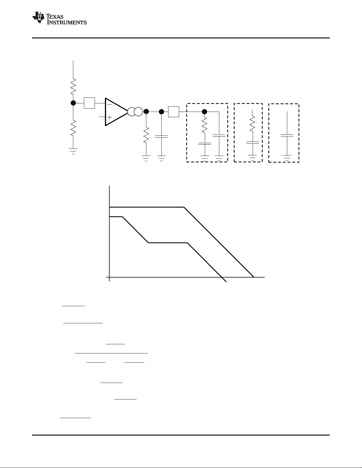
Fixed Frequency PWM Control
The TPS54240 uses an adjustable fixed frequency, peak current mode control. The output voltage is compared
through external resistors on the VSENSE pin to an internal voltage reference by an error amplifier which drives
the COMP pin. An internal oscillator initiates the turn on of the high side power switch. The error amplifier output
is compared to the high side power switch current. When the power switch current reaches the level set by the
COMP voltage, the power switch is turned off. The COMP pin voltage will increase and decrease as the output
current increases and decreases. The device implements a current limit by clamping the COMP pin voltage to a
maximum level. The Eco-Mode™ is implemented with a minimum clamp on the COMP pin.
Slope Compensation Output Current
The TPS54240 adds a compensating ramp to the switch current signal. This slope compensation prevents
sub-harmonic oscillations. The available peak inductor current remains constant over the full duty cycle range.
Pulse Skip Eco-Mode
The TPS54240 operates in a pulse skip Eco mode at light load currents to improve efficiency by reducing
switching and gate drive losses. The TPS54240 is designed so that if the output voltage is within regulation and
the peak switch current at the end of any switching cycle is below the pulse skipping current threshold, the
device enters Eco mode. This current threshold is the current level corresponding to a nominal COMP voltage or
500mV.
When in Eco-mode, the COMP pin voltage is clamped at 500mV and the high side MOSFET is inhibited. Further
decreases in load current or in output voltage can not drive the COMP pin below this clamp voltage level.
Since the device is not switching, the output voltage begins to decay. As the voltage control loop compensates
for the falling output voltage, the COMP pin voltage begins to rise. At this time, the high side MOSFET is enabled
and a switching pulse initiates on the next switching cycle. The peak current is set by the COMP pin voltage. The
output voltage re-charges the regulated value, then the peak switch current starts to decrease, and eventually
falls below the Eco mode threshold at which time the device again enters Eco mode.
For Eco mode operation, the TPS54240 senses peak current, not average or load current, so the load current
where the device enters Eco mode is dependent on the output inductor value. For example, the circuit in
Figure 49 enters Eco mode at about 5 mA of output current. When the load current is low and the output voltage
is within regulation, the device enters a sleep mode and draws only 138mA input quiescent current. The internal
PLL remains operating when in sleep mode. When operating at light load currents in the pulse skip mode, the
switching transitions occur synchronously with the external clock signal.
Low Dropout Operation and Bootstrap Voltage (BOOT)
The TPS54240 has an integrated boot regulator, and requires a small ceramic capacitor between the BOOT and
PH pins to provide the gate drive voltage for the high side MOSFET. The BOOT capacitor is refreshed when the
high side MOSFET is off and the low side diode conducts. The value of this ceramic capacitor should be 0.1mF.
A ceramic capacitor with an X7R or X5R grade dielectric with a voltage rating of 10V or higher is recommended
because of the stable characteristics overtemperature and voltage.
To improve drop out, the TPS54240 is designed to operate at 100% duty cycle as long as the BOOT to PH pin
voltage is greater than 2.1V. When the voltage from BOOT to PH drops below 2.1V, the high side MOSFET is
turned off using an UVLO circuit which allows the low side diode to conduct and refresh the charge on the BOOT
capacitor. Since the supply current sourced from the BOOT capacitor is low, the high side MOSFET can remain
on for more switching cycles than are required to refresh the capacitor, thus the effective duty cycle of the
switching regulator is high.
The effective duty cycle during dropout of the regulator is mainly influenced by the voltage drops across the
power MOSFET, inductor resistance, low side diode and printed circuit board resistance. During operating
conditions in which the input voltage drops and the regulator is operating in continuous conduction mode, the
high side MOSFET can remain on for 100% of the duty cycle to maintain output regulation, until the BOOT to PH
voltage falls below 2.1V.
12 Submit Documentation Feedback Copyright © 2010, Texas Instruments Incorporated
Product Folder Link(s): TPS54240
Page 13
4.6
4.8
5
5.2
5.4
5.6
0 0.05 0.10 0.15 0.20
I -OutputCurrent- A
O
V -InputVoltage-V
I
V =5V
O
Start
Stop
3
3.2
3.4
3.6
3.8
4
0 0.05 0.10 0.15 0.20
I -OutputCurrent- A
O
V -InputVoltage-V
I
V =3.3V
O
Start
Stop
TPS54240
www.ti.com
SLVSAA6 –APRIL 2010
DETAILED DESCRIPTION (continued)
Attention must be taken in maximum duty cycle applications which experience extended time periods with light
loads or no load. When the voltage across the BOOT capacitor falls below the 2.1V UVLO threshold, the high
side MOSFET is turned off, but there may not be enough inductor current to pull the PH pin down to recharge the
BOOT capacitor. The high side MOSFET of the regulator stops switching because the voltage across the BOOT
capacitor is less than 2.1V. The output capacitor then decays until the difference in the input voltage and output
voltage is greater than 2.1V, at which point the BOOT UVLO threshold is exceeded, and the device starts
switching again until the desired output voltage is reached. This operating condition persists until the input
voltage and/or the load current increases. It is recommended to adjust the VIN stop voltage greater than the
BOOT UVLO trigger condition at the minimum load of the application using the adjustable VIN UVLO feature with
resistors on the EN pin.
The start and stop voltages for typical 3.3V and 5V output applications are shown in Figure 25 and Figure 26.
The voltages are plotted versus load current. The start voltage is defined as the input voltage needed to regulate
the output within 1%. The stop voltage is defined as the input voltage at which the output drops by 5% or stops
switching.
During high duty cycle conditions, the inductor current ripple increases while the BOOT capacitor is being
recharged resulting in an increase in ripple voltage on the output. This is due to the recharge time of the boot
capacitor being longer than the typical high side off time when switching occurs every cycle.
Figure 25. 3.3V Start/Stop Voltage Figure 26. 5.0V Start/Stop Voltage
Error Amplifier
The TPS54240 has a transconductance amplifier for the error amplifier. The error amplifier compares the
VSENSE voltage to the lower of the SS/TR pin voltage or the internal 0.8V voltage reference. The
transconductance (gm) of the error amplifier is 310mA/V during normal operation. During the slow start operation,
the transconductance is a fraction of the normal operating gm. When the voltage of the VSENSE pin is below
0.8V and the device is regulating using the SS/TR voltage, the gm is 70mA/V.
The frequency compensation components (capacitor, series resistor and capacitor) are added to the COMP pin
to ground.
Voltage Reference
The voltage reference system produces a precise ±2% voltage reference over temperature by scaling the output
of a temperature stable bandgap circuit.
Adjusting the Output Voltage
The output voltage is set with a resistor divider from the output node to the VSENSE pin. It is recommended to
use 1% tolerance or better divider resistors. Start with a 10 kΩ for the R2 resistor and use the Equation 1 to
calculate R1. To improve efficiency at light loads consider using larger value resistors. If the values are too high
the regulator will be more susceptible to noise and voltage errors from the VSENSE input current will be
noticeable.
Copyright © 2010, Texas Instruments Incorporated Submit Documentation Feedback 13
Product Folder Link(s): TPS54240
Page 14
Vout 0.8V
R1 = R2
0.8 V
-
æ ö
´
ç ÷
è ø
EN
VIN
+
-
TPS54240
R1
R2
Ihys
I1
0.9 Am
1.25V
2.9 Am
START STOP
HYS
V V
R1
I
-
=
ENA
START ENA
1
V
R2
V V
I
R1
=
+
EN
Ihys
VIN
+
-
TPS54240
R1
R2
VOUT
R3
I1
0.9 Am
2.9 Am
1.25V
TPS54240
SLVSAA6 –APRIL 2010
www.ti.com
DETAILED DESCRIPTION (continued)
(1)
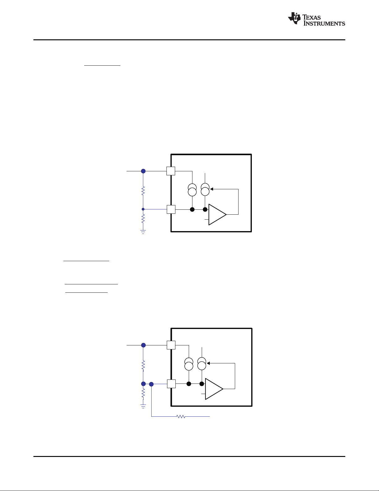
Enable and Adjusting Undervoltage Lockout
The TPS54240 is disabled when the VIN pin voltage falls below 2.5 V. If an application requires a higher
undervoltage lockout (UVLO), use the EN pin as shown in Figure 27 to adjust the input voltage UVLO by using
the two external resistors. Though it is not necessary to use the UVLO adjust registers, for operation it is highly
recommended to provide consistent power up behavior. The EN pin has an internal pull-up current source, I1, of
0.9mA that provides the default condition of the TPS54240 operating when the EN pin floats. Once the EN pin
voltage exceeds 1.25V, an additional 2.9mA of hysteresis, Ihys, is added. This additional current facilitates input
voltage hysteresis. Use Equation 2 to set the external hysteresis for the input voltage. Use Equation 3 to set the
input start voltage.
Figure 27. Adjustable Undervoltage Lockout (UVLO)
Another technique to add input voltage hysteresis is shown in Figure 28. This method may be used, if the
resistance values are high from the previous method and a wider voltage hysteresis is needed. The resistor R3
sources additional hysteresis current into the EN pin.
Figure 28. Adding Additional Hysteresis
Product Folder Link(s): TPS54240
14 Submit Documentation Feedback Copyright © 2010, Texas Instruments Incorporated
(2)
(3)
Page 15
STA RT S TOP
OUT
HYS
V V
R1
V
I
R3
-
=
+
ENA
START ENA
ENA
1
V
R2
V V
V
I
R1 R3
=
+ -
Tss(ms) Iss( A)
Css(nF) =
Vref (V) 0.8
m´
´
EN
SS/TR
V
SENSE
VOUT
TPS54240
www.ti.com
SLVSAA6 –APRIL 2010
DETAILED DESCRIPTION (continued)
(4)
(5)
Slow Start/Tracking Pin (SS/TR)
The TPS54240 effectively uses the lower voltage of the internal voltage reference or the SS/TR pin voltage as
the power-supply's reference voltage and regulates the output accordingly. A capacitor on the SS/TR pin to
ground implements a slow start time. The TPS54240 has an internal pull-up current source of 2mA that charges
the external slow start capacitor. The calculations for the slow start time (10% to 90%) are shown in Equation 6.
The voltage reference (V
remain lower than 0.47mF and greater than 0.47nF.
At power up, the TPS54240 will not start switching until the slow start pin is discharged to less than 40 mV to
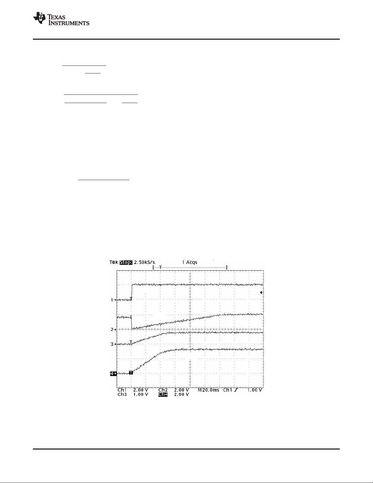
ensure a proper power up, see Figure 29.
Also, during normal operation, the TPS54240 will stop switching and the SS/TR must be discharged to 40 mV,
when the VIN UVLO is exceeded, EN pin pulled below 1.25V, or a thermal shutdown event occurs.
The VSENSE voltage will follow the SS/TR pin voltage with a 45mV offset up to 85% of the internal voltage
reference. When the SS/TR voltage is greater than 85% on the internal reference voltage the offset increases as
the effective system reference transitions from the SS/TR voltage to the internal voltage reference (see
Figure 23). The SS/TR voltage will ramp linearly until clamped at 1.7V.
) is 0.8 V and the slow start current (ISS) is 2mA. The slow start capacitor should
REF
(6)
Copyright © 2010, Texas Instruments Incorporated Submit Documentation Feedback 15
Figure 29. Operation of SS/TR Pin when Starting
Product Folder Link(s): TPS54240
Page 16

SS /TR
TPS54240
EN
PWRGD
SS /TR
EN
PWRGD
EN1
PWRGD1
VOUT1
VOUT2
TPS54240
SLVSAA6 –APRIL 2010
www.ti.com
DETAILED DESCRIPTION (continued)
Overload Recovery Circuit
The TPS54240 has an overload recovery (OLR) circuit. The OLR circuit will slow start the output from the
overload voltage to the nominal regulation voltage once the fault condition is removed. The OLR circuit will
discharge the SS/TR pin to a voltage slightly greater than the VSENSE pin voltage using an internal pull down of
382mA when the error amplifier is changed to a high voltage from a fault condition. When the fault condition is
removed, the output will slow start from the fault voltage to nominal output voltage.
Sequencing
Many of the common power supply sequencing methods can be implemented using the SS/TR, EN and PWRGD
pins. The sequential method can be implemented using an open drain output of a power on reset pin of another
device. The sequential method is illustrated in Figure 30 using two TPS54240 devices. The power good is
coupled to the EN pin on the TPS54240 which will enable the second power supply once the primary supply
reaches regulation. If needed, a 1nF ceramic capacitor on the EN pin of the second power supply will provide a
1ms start up delay. Figure 31 shows the results of Figure 30.
Figure 30. Schematic for Sequential Start-Up Figure 31. Sequential Startup using EN and
Sequence PWRGD
Product Folder Link(s): TPS54240
16 Submit Documentation Feedback Copyright © 2010, Texas Instruments Incorporated
Page 17

EN1,EN2
VOUT1
VOUT2
EN
TPS54160
3
SS/TR
4
PWRGD6
EN
TPS54160
3
SS/TR
4
PWRGD6
TPS54240
TPS54240
SS/TR
TPS54240
EN
PWRGD
SS/ TR
EN
PWRGD
VOUT 1
VOUT 2
R 1
R 2
R3
R 4
TPS54240
TPS54240
www.ti.com
SLVSAA6 –APRIL 2010
DETAILED DESCRIPTION (continued)
Figure 32. Schematic for Ratiometric Start-Up Figure 33. Ratio-Metric Startup using Coupled
Sequence SS/TR pins
Figure 32 shows a method for ratio-metric start up sequence by connecting the SS/TR pins together. The
regulator outputs will ramp up and reach regulation at the same time. When calculating the slow start time the
pull up current source must be doubled in Equation 6. Figure 33 shows the results of Figure 32.
Copyright © 2010, Texas Instruments Incorporated Submit Documentation Feedback 17
Figure 34. Schematic for Ratiometric and Simultaneous Start-Up Sequence
Product Folder Link(s): TPS54240
Page 18

Vout2 + deltaV Vssoffset
R1 =
VREF Iss
´
VREF R1
R2 =
Vout2 + deltaV VREF
´
-
deltaV = Vout1 Vout2-
R1 > 2800 Vout1 180 deltaV´ - ´
EN
VOUT1
VOUT2
EN
VOUT1
VOUT2
TPS54240
SLVSAA6 –APRIL 2010
www.ti.com
DETAILED DESCRIPTION (continued)
Ratio-metric and simultaneous power supply sequencing can be implemented by connecting the resistor network
of R1 and R2 shown in Figure 34 to the output of the power supply that needs to be tracked or another voltage
reference source. Using Equation 7 and Equation 8, the tracking resistors can be calculated to initiate the Vout2
slightly before, after or at the same time as Vout1. Equation 9 is the voltage difference between Vout1 and Vout2
at the 95% of nominal output regulation.
The deltaV variable is zero volts for simultaneous sequencing. To minimize the effect of the inherent SS/TR to
VSENSE offset (Vssoffset) in the slow start circuit and the offset created by the pullup current source (Iss) and
tracking resistors, the Vssoffset and Iss are included as variables in the equations.
To design a ratio-metric start up in which the Vout2 voltage is slightly greater than the Vout1 voltage when Vout2
reaches regulation, use a negative number in Equation 7 through Equation 9 for deltaV. Equation 9 will result in a
positive number for applications which the Vout2 is slightly lower than Vout1 when Vout2 regulation is achieved.
Since the SS/TR pin must be pulled below 40mV before starting after an EN, UVLO or thermal shutdown fault,
careful selection of the tracking resistors is needed to ensure the device will restart after a fault. Make sure the
calculated R1 value from Equation 7 is greater than the value calculated in Equation 10 to ensure the device can
recover from a fault.
As the SS/TR voltage becomes more than 85% of the nominal reference voltage the Vssoffset becomes larger
as the slow start circuits gradually handoff the regulation reference to the internal voltage reference. The SS/TR
pin voltage needs to be greater than 1.3V for a complete handoff to the internal voltage reference as shown in
Figure 23.
(7)
Figure 35. Ratio-metric Startup with Tracking Figure 36. Ratiometric Startup with Tracking
Resistors Resistors
(8)
(9)
(10)
18 Submit Documentation Feedback Copyright © 2010, Texas Instruments Incorporated
Product Folder Link(s): TPS54240
Page 19

EN
VOUT1
VOUT2
TPS54240
www.ti.com
SLVSAA6 –APRIL 2010
DETAILED DESCRIPTION (continued)
Figure 37. Simultaneous Startup With Tracking Resistor
Copyright © 2010, Texas Instruments Incorporated Submit Documentation Feedback 19
Product Folder Link(s): TPS54240
Page 20

RT kOhm
sw kHz
1.0888
206033
( ) =
¦ ( )
0
100
200
300
400
500
200 300 400 500 600 700 800 900 1000 1100
RT/CLK-Resistance-kW
f -SwitchingFrequency-kHz
s
1200
V =12V,
T =25°C
I
J
0
500
1000
1500
2000
2500
0 25 50 75 100 125 150 175 200
f -SwitchingFrequency-kHz
s
RT/CLK-ClockResistance-kW
V =12V,
T =25°C
I
J
TPS54240
SLVSAA6 –APRIL 2010
www.ti.com
DETAILED DESCRIPTION (continued)
Constant Switching Frequency and Timing Resistor (RT/CLK Pin)
The switching frequency of the TPS54240 is adjustable over a wide range from approximately 100kHz to
2500kHz by placing a resistor on the RT/CLK pin. The RT/CLK pin voltage is typically 0.5V and must have a
resistor to ground to set the switching frequency. To determine the timing resistance for a given switching
frequency, use Equation 11 or the curves in Figure 38 or Figure 39. To reduce the solution size one would
typically set the switching frequency as high as possible, but tradeoffs of the supply efficiency, maximum input
voltage and minimum controllable on time should be considered.
The minimum controllable on time is typically 135ns and limits the maximum operating input voltage.
The maximum switching frequency is also limited by the frequency shift circuit. More discussion on the details of
the maximum switching frequency is located below.
(11)
SWITCHING FREQUENCY SWITCHING FREQUENCY
RT/CLK RESISTANCE HIGH FREQUENCY RANGE RT/CLK RESISTANCE LOW FREQUENCY RANGE
vs vs
Figure 38. High Range RT Figure 39. Low Range RT
Overcurrent Protection and Frequency Shift
The TPS54240 implements current mode control which uses the COMP pin voltage to turn off the high side
MOSFET on a cycle by cycle basis. Each cycle the switch current and COMP pin voltage are compared, when
the peak switch current intersects the COMP voltage, the high side switch is turned off. During overcurrent
conditions that pull the output voltage low, the error amplifier will respond by driving the COMP pin high,
increasing the switch current. The error amplifier output is clamped internally, which functions as a switch current
limit.
To increase the maximum operating switching frequency at high input voltages the TPS54240 implements a
frequency shift. The switching frequency is divided by 8, 4, 2, and 1 as the voltage ramps from 0 to 0.8 volts on
VSENSE pin.
The device implements a digital frequency shift to enable synchronizing to an external clock during normal
startup and fault conditions. Since the device can only divide the switching frequency by 8, there is a maximum
input voltage limit in which the device operates and still have frequency shift protection.
During short-circuit events (particularly with high input voltage applications), the control loop has a finite minimum
controllable on time and the output has a low voltage. During the switch on time, the inductor current ramps to
the peak current limit because of the high input voltage and minimum on time. During the switch off time, the
inductor would normally not have enough off time and output voltage for the inductor to ramp down by the ramp
up amount. The frequency shift effectively increases the off time allowing the current to ramp down.
20 Submit Documentation Feedback Copyright © 2010, Texas Instruments Incorporated
Product Folder Link(s): TPS54240
Page 21
( )
( )
( )
L OUT
SW max skip
ON IN L
I Rdc V Vd
1
t V I Rhs Vd
æ ö
´ + +
æ ö
= ´
ç ÷
ç ÷
ç ÷
- ´ +
è ø
è ø
f
( )
( )
L OUTSC
SW shift
ON IN L
(I Rdc V Vd)
div
t V I x Rhs Vd
æ ö
´ + +
= ´
ç ÷
ç ÷
- +
è ø
f
f
10
20 30
40
2500
2000
1500
1000
500
0
f -SwitchingFrequency-kHz
s
V -InputVoltage-V
I
Skip
Shift
V =3.3V
O
TPS54240
www.ti.com
SLVSAA6 –APRIL 2010
DETAILED DESCRIPTION (continued)
Selecting the Switching Frequency
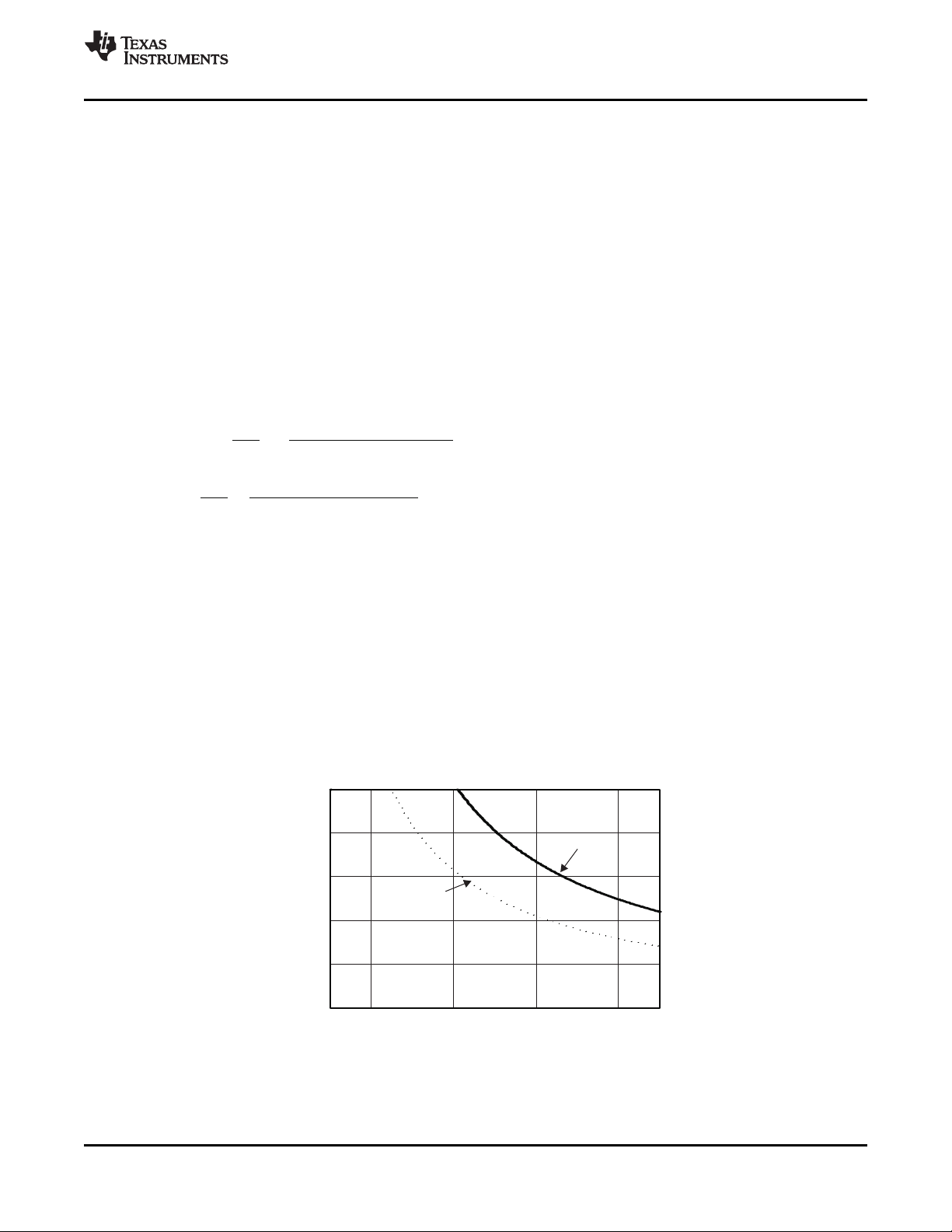
The switching frequency that is selected should be the lower value of the two equations, Equation 12 and
Equation 13. Equation 12 is the maximum switching frequency limitation set by the minimum controllable on time.
Setting the switching frequency above this value will cause the regulator to skip switching pulses.
Equation 13 is the maximum switching frequency limit set by the frequency shift protection. To have adequate
output short circuit protection at high input voltages, the switching frequency should be set to be less than the
fsw(maxshift) frequency. In Equation 13, to calculate the maximum switching frequency one must take into
account that the output voltage decreases from the nominal voltage to 0 volts, the fdiv integer increases from 1 to
8 corresponding to the frequency shift.
In Figure 40, the solid line illustrates a typical safe operating area regarding frequency shift and assumes the
output voltage is zero volts, and the resistance of the inductor is 0.130Ω, FET on resistance of 0.2Ω and the
diode voltage drop is 0.5V. The dashed line is the maximum switching frequency to avoid pulse skipping. Enter
these equations in a spreadsheet or other software or use the SwitcherPro design software to determine the
switching frequency.
(12)
(13)
I
L
inductor current
Rdc inductor resistance
V
IN
V
OUT
V
OUTSC
maximum input voltage
output voltage
output voltage during short
Vd diode voltage drop
R
t
ON
ƒ
DIV
DS(on)
switch on resistance
controllable on time
frequency divide equals (1, 2, 4, or 8)
Copyright © 2010, Texas Instruments Incorporated Submit Documentation Feedback 21
Figure 40. Maximum Switching Frequency vs. Input Voltage
Product Folder Link(s): TPS54240
Page 22
RT/CLK
TPS54240
Clock
Source
PLL
R
fset
10pF
4kW
50 W
EXT
TPS54240
SLVSAA6 –APRIL 2010
www.ti.com
DETAILED DESCRIPTION (continued)
How to Interface to RT/CLK Pin
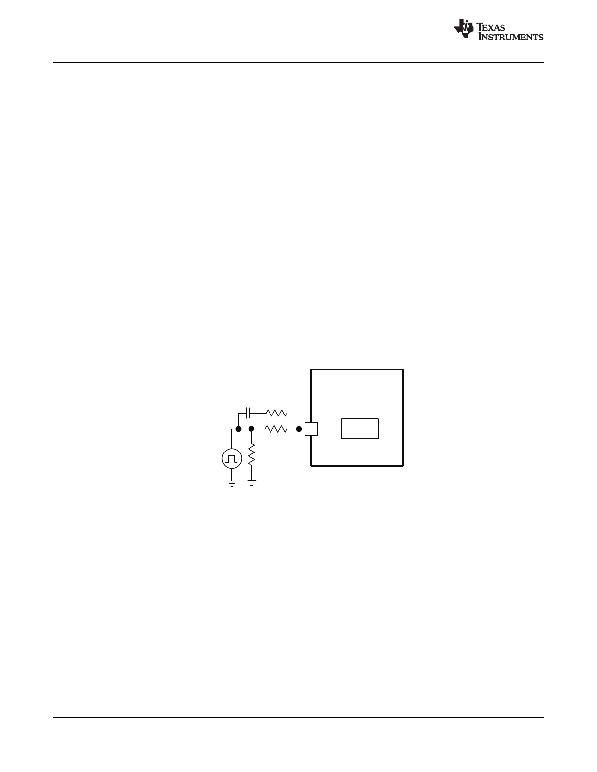
The RT/CLK pin can be used to synchronize the regulator to an external system clock. To implement the
synchronization feature connect a square wave to the RT/CLK pin through the circuit network shown in
Figure 41. The square wave amplitude must transition lower than 0.5V and higher than 2.2V on the RT/CLK pin
and have an on time greater than 40 ns and an off time greater than 40 ns. The synchronization frequency range
is 300 kHz to 2200 kHz. The rising edge of the PH will be synchronized to the falling edge of RT/CLK pin signal.
The external synchronization circuit should be designed in such a way that the device will have the default
frequency set resistor connected from the RT/CLK pin to ground should the synchronization signal turn off. It is
recommended to use a frequency set resistor connected as shown in Figure 41 through a 50Ω resistor to
ground. The resistor should set the switching frequency close to the external CLK frequency. It is recommended
to ac couple the synchronization signal through a 10 pF ceramic capacitor to RT/CLK pin and a 4kΩ series
resistor. The series resistor reduces PH jitter in heavy load applications when synchronizing to an external clock
and in applications which transition from synchronizing to RT mode. The first time the CLK is pulled above the
CLK threshold the device switches from the RT resistor frequency to PLL mode. The internal 0.5V voltage source
is removed and the CLK pin becomes high impedance as the PLL starts to lock onto the external signal. Since
there is a PLL on the regulator the switching frequency can be higher or lower than the frequency set with the
external resistor. The device transitions from the resistor mode to the PLL mode and then will increase or
decrease the switching frequency until the PLL locks onto the CLK frequency within 100 microseconds.
When the device transitions from the PLL to resistor mode the switching frequency will slow down from the CLK
frequency to 150 kHz, then reapply the 0.5V voltage and the resistor will then set the switching frequency. The
switching frequency is divided by 8, 4, 2, and 1 as the voltage ramps from 0 to 0.8 volts on VSENSE pin. The
device implements a digital frequency shift to enable synchronizing to an external clock during normal startup
and fault conditions. Figure 42, Figure 43 and Figure 44 show the device synchronized to an external system
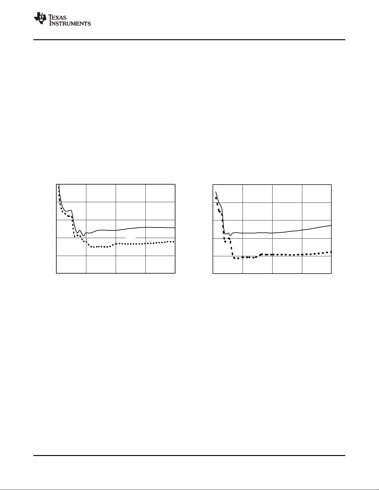
clock in continuous conduction mode (ccm) discontinuous conduction (dcm) and pulse skip mode (psm).
Figure 41. Synchronizing to a System Clock
22 Submit Documentation Feedback Copyright © 2010, Texas Instruments Incorporated
Product Folder Link(s): TPS54240
Page 23

IL
EXT
PH
EXT
IL
PH
EXT
IL
PH
TPS54240
www.ti.com
SLVSAA6 –APRIL 2010
DETAILED DESCRIPTION (continued)
Figure 42. Plot of Synchronizing in ccm Figure 43. Plot of Synchronizing in dcm
Figure 44. Plot of Synchronizing in PSM
Power Good (PWRGD Pin)
The PWRGD pin is an open drain output. Once the VSENSE pin is between 94% and 107% of the internal
voltage reference the PWRGD pin is de-asserted and the pin floats. It is recommended to use a pull-up resistor
between the values of 10 and 100kΩ to a voltage source that is 5.5V or less. The PWRGD is in a defined state
once the VIN input voltage is greater than 1.5V but with reduced current sinking capability. The PWRGD will
achieve full current sinking capability as VIN input voltage approaches 3V.
Copyright © 2010, Texas Instruments Incorporated Submit Documentation Feedback 23
Product Folder Link(s): TPS54240
Page 24

TPS54240
SLVSAA6 –APRIL 2010
www.ti.com
DETAILED DESCRIPTION (continued)
The PWRGD pin is pulled low when the VSENSE is lower than 92% or greater than 109% of the nominal internal
reference voltage. Also, the PWRGD is pulled low, if the UVLO or thermal shutdown are asserted or the EN pin
pulled low.
Overvoltage Transient Protection
The TPS54240 incorporates an overvoltage transient protection (OVTP) circuit to minimize voltage overshoot
when recovering from output fault conditions or strong unload transients on power supply designs with low value
output capacitance. For example, when the power supply output is overloaded the error amplifier compares the
actual output voltage to the internal reference voltage. If the VSENSE pin voltage is lower than the internal
reference voltage for a considerable time, the output of the error amplifier will respond by clamping the error
amplifier output to a high voltage. Thus, requesting the maximum output current. Once the condition is removed,
the regulator output rises and the error amplifier output transitions to the steady state duty cycle. In some
applications, the power supply output voltage can respond faster than the error amplifier output can respond, this
actuality leads to the possibility of an output overshoot. The OVTP feature minimizes the output overshoot, when
using a low value output capacitor, by implementing a circuit to compare the VSENSE pin voltage to OVTP
threshold which is 109% of the internal voltage reference. If the VSENSE pin voltage is greater than the OVTP
threshold, the high side MOSFET is disabled preventing current from flowing to the output and minimizing output
overshoot. When the VSENSE voltage drops lower than the OVTP threshold, the high side MOSFET is allowed
to turn on at the next clock cycle.
Thermal Shutdown
The device implements an internal thermal shutdown to protect itself if the junction temperature exceeds 182°C.
The thermal shutdown forces the device to stop switching when the junction temperature exceeds the thermal
trip threshold. Once the die temperature decreases below 182°C, the device reinitiates the power up sequence
by discharging the SS/TR pin.
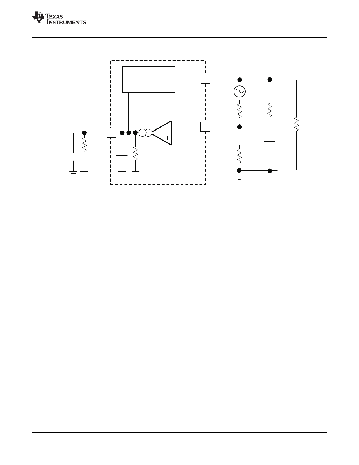
Small Signal Model for Loop Response
Figure 45 shows an equivalent model for the TPS54240 control loop which can be modeled in a circuit simulation
program to check frequency response and dynamic load response. The error amplifier is a transconductance
amplifier with a gmEAof 310 mA/V. The error amplifier can be modeled using an ideal voltage controlled current
source. The resistor Roand capacitor Comodel the open loop gain and frequency response of the amplifier. The
1mV ac voltage source between the nodes a and b effectively breaks the control loop for the frequency response
measurements. Plotting c/a shows the small signal response of the frequency compensation. Plotting a/b shows
the small signal response of the overall loop. The dynamic loop response can be checked by replacing RLwith a
current source with the appropriate load step amplitude and step rate in a time domain analysis. This equivalent
model is only valid for continuous conduction mode designs.
24 Submit Documentation Feedback Copyright © 2010, Texas Instruments Incorporated
Product Folder Link(s): TPS54240
Page 25
VSENSE
COMP
V
O
R1
R3
C1
C2
R2
CO RO
gm
ea
310 A/Vm
0.8V
PowerStage
gm 10.5 A/V
ps
PH
R
ESR
C
OUT
R
L
b
a
c
TPS54240
www.ti.com
SLVSAA6 –APRIL 2010
DETAILED DESCRIPTION (continued)
Figure 45. Small Signal Model for Loop Response
Simple Small Signal Model for Peak Current Mode Control
Figure 46 describes a simple small signal model that can be used to understand how to design the frequency
compensation. The TPS54240 power stage can be approximated to a voltage-controlled current source (duty
cycle modulator) supplying current to the output capacitor and load resistor. The control to output transfer
function is shown in Equation 14 and consists of a dc gain, one dominant pole, and one ESR zero. The quotient
of the change in switch current and the change in COMP pin voltage (node c in Figure 45) is the power stage
transconductance. The gmPSfor the TPS54240 is 10.5 A/V. The low-frequency gain of the power stage
frequency response is the product of the transconductance and the load resistance as shown in Equation 15.
As the load current increases and decreases, the low-frequency gain decreases and increases, respectively. This
variation with the load may seem problematic at first glance, but fortunately the dominant pole moves with the
load current (see Equation 16). The combined effect is highlighted by the dashed line in the right half of
Figure 46. As the load current decreases, the gain increases and the pole frequency lowers, keeping the 0-dB
crossover frequency the same for the varying load conditions which makes it easier to design the frequency
compensation. The type of output capacitor chosen determines whether the ESR zero has a profound effect on
the frequency compensation design. Using high ESR aluminum electrolytic capacitors may reduce the number
frequency compensation components needed to stabilize the overall loop because the phase margin increases
from the ESR zero at the lower frequencies (see Equation 17).
Copyright © 2010, Texas Instruments Incorporated Submit Documentation Feedback 25
Product Folder Link(s): TPS54240
Page 26

V
O
R
ESR
C
OUT
R
L
VC
gm
ps
fp
fz
Adc
Z
OUT
C
P
s
1
2
V
Adc
V
s
1
2
æ ö
+
ç ÷
p ´
è ø
= ´
æ ö
+
ç ÷
p ´
è ø
f
f
ps L
Adc = gm R´
P
OUT L
1
f
C R 2
=
´ ´ p
Z
OUT ESR
1
C R 2
=
´ ´ p
f
TPS54240
SLVSAA6 –APRIL 2010
DETAILED DESCRIPTION (continued)
Figure 46. Simple Small Signal Model and Frequency Response for Peak Current Mode Control
www.ti.com
(14)
(15)
(16)
(17)
Small Signal Model for Frequency Compensation
The TPS54240 uses a transconductance amplifier for the error amplifier and readily supports three of the
commonly-used frequency compensation circuits. Compensation circuits Type 2A, Type 2B, and Type 1 are
shown in Figure 47. Type 2 circuits most likely implemented in high bandwidth power-supply designs using low
ESR output capacitors. The Type 1 circuit is used with power-supply designs with high-ESR aluminum
electrolytic or tantalum capacitors.. Equation 18 and Equation 19 show how to relate the frequency response of
the amplifier to the small signal model in Figure 47. The open-loop gain and bandwidth are modeled using the R
and COshown in Figure 47. See the application section for a design example using a Type 2A network with a
low ESR output capacitor.
Equation 18 through Equation 27 are provided as a reference for those who prefer to compensate using the
preferred methods. Those who prefer to use prescribed method use the method outlined in the application
section or use switched information.
O
26 Submit Documentation Feedback Copyright © 2010, Texas Instruments Incorporated
Product Folder Link(s): TPS54240
Page 27
Vref
V
O
R1
R3
C1
C2
R2
C
O
R
O
gm
ea
COMP
VSENSE
Type2A Type2B Type1
C2
R3
C1
A0
A1
P1
Z1
P2
Aol
BW
ea
Aol(V/V)
Ro =
gm
p ´
ea
O
gm
C =
2 BW (Hz)
f
f f
Z1
P1 P2
s
1
2
EA A0
s s
1 1
2 2
æ ö
+
ç ÷
p ´
è ø
= ´
æ ö æ ö
+ ´ +
ç ÷ ç ÷
p ´ p ´
è ø è ø
ea
R2
A0 = gm Ro
R1 + R2
´ ´
ea
R2
A1 = gm Ro| | R3
R1 + R2
´ ´
1
P1
2 Ro C1
=
p ´ ´
TPS54240
www.ti.com
SLVSAA6 –APRIL 2010
DETAILED DESCRIPTION (continued)
Figure 47. Types of Frequency Compensation
Copyright © 2010, Texas Instruments Incorporated Submit Documentation Feedback 27
Figure 48. Frequency Response of the Type 2A and Type 2B Frequency Compensation
Product Folder Link(s): TPS54240
(18)
(19)
(20)
(21)
(22)
(23)
Page 28

1
Z1
2 R3 C1
=
p ´ ´
p ´ ´
O O
1
P2 = type 2a
2 R3 | | R (C2 + C )
p ´ ´
O O
1
P2 = type 2b
2 R3 | | R C
p ´ ´
O O
1
P2 = type 1
2 R (C2 + C )
TPS54240
SLVSAA6 –APRIL 2010
www.ti.com
DETAILED DESCRIPTION (continued)
(24)
(25)
(26)
(27)
28 Submit Documentation Feedback Copyright © 2010, Texas Instruments Incorporated
Product Folder Link(s): TPS54240
Page 29

TPS54240
www.ti.com
SLVSAA6 –APRIL 2010
APPLICATION INFORMATION
Design Guide — Step-By-Step Design Procedure
This example details the design of a high frequency switching regulator design using ceramic output capacitors.
A few parameters must be known in order to start the design process. These parameters are typically determined
at the system level. For this example, we will start with the following known parameters:
Output Voltage 3.3 V
Transient Response 0 to 1.5A load step ΔVout = 3 %
Maximum Output Current 2.5 A
Input Voltage 12 V nom. 10.8 V to 13.2 V
Output Voltage Ripple 1% of Vout
Start Input Voltage (rising VIN) 6.0 V
Stop Input Voltage (falling VIN) 5.5 V
Selecting the Switching Frequency
The first step is to decide on a switching frequency for the regulator. Typically, the user will want to choose the
highest switching frequency possible since this will produce the smallest solution size. The high switching
frequency allows for lower valued inductors and smaller output capacitors compared to a power supply that
switches at a lower frequency. The switching frequency that can be selected is limited by the minimum on-time of
the internal power switch, the input voltage and the output voltage and the frequency shift limitation.
Equation 12 and Equation 13 must be used to find the maximum switching frequency for the regulator, choose
the lower value of the two equations. Switching frequencies higher than these values will result in pulse skipping
or the lack of overcurrent protection during a short circuit.
The typical minimum on time, t
and the maximum input voltage is 13.2 V, which allows for a maximum switch frequency up to 2247 kHz when
including the inductor resistance, on resistance output current and diode voltage in Equation 12. To ensure
overcurrent runaway is not a concern during short circuits in your design use Equation 13 or the solid curve in
Figure 40 to determine the maximum switching frequency. With a maximum input voltage of 13.2 V, assuming a
diode voltage of 0.7 V, inductor resistance of 26 mΩ, switch resistance of 200 mΩ, a current limit value of 3.5 A
and a short circuit output voltage of 0.2 V. The maximum switching frequency is approximately 4449 kHz.
For this design, a much lower switching frequency of 300 kHz is used. To determine the timing resistance for a
given switching frequency, use Equation 11 or the curve in Figure 39.
The switching frequency is set by resistor R3shown in Figure 49 For 300 kHz operation a 412 kΩ resistor is
required.
, is 135 ns for the TPS54240. For this example, the output voltage is 3.3 V
onmin
Copyright © 2010, Texas Instruments Incorporated Submit Documentation Feedback 29
Product Folder Link(s): TPS54240
Page 30

TPS54240DGQ
IND
Vinmax Vout Vout
Lo min =
Io K Vinmax ƒsw
´
´ ´
TPS54240
SLVSAA6 –APRIL 2010
www.ti.com
Figure 49. 3.3V Output TPS54240 Design Example.
Output Inductor Selection (LO)
To calculate the minimum value of the output inductor, use Equation 28.
K
is a coefficient that represents the amount of inductor ripple current relative to the maximum output current.
IND
The inductor ripple current will be filtered by the output capacitor. Therefore, choosing high inductor ripple
currents will impact the selection of the output capacitor since the output capacitor must have a ripple current
rating equal to or greater than the inductor ripple current. In general, the inductor ripple value is at the discretion
of the designer; however, the following guidelines may be used.
For designs using low ESR output capacitors such as ceramics, a value as high as K
When using higher ESR output capacitors, K
= 0.2 yields better results. Since the inductor ripple current is
IND
part of the PWM control system, the inductor ripple current should always be greater than 150 mA for
dependable operation. In a wide input voltage regulator, it is best to choose an inductor ripple current on the
larger side. This allows the inductor to still have a measurable ripple current with the input voltage at its
minimum.
For this design example, use K
= 0.3 and the minimum inductor value is calculated to be 11 mH. For this
IND
design, a nearest standard value was chosen: 10 mH. For the output filter inductor, it is important that the RMS
current and saturation current ratings not be exceeded. The RMS and peak inductor current can be found from
Equation 30 and Equation 31.
For this design, the RMS inductor current is 2.51 A and the peak inductor current is 2.913 A. The chosen
inductor is a Coilcraft MSS1038-103NLB . It has a saturation current rating of 4.52 A and an RMS current rating
of 4.05 A.
As the equation set demonstrates, lower ripple currents will reduce the output voltage ripple of the regulator but
will require a larger value of inductance. Selecting higher ripple currents will increase the output voltage ripple of
the regulator but allow for a lower inductance value.
The current flowing through the inductor is the inductor ripple current plus the output current. During power up,
faults or transient load conditions, the inductor current can increase above the calculated peak inductor current
level calculated above. In transient conditions, the inductor current can increase up to the switch current limit of
the device. For this reason, the most conservative approach is to specify an inductor with a saturation current
rating equal to or greater than the switch current limit rather than the peak inductor current.
= 0.3 may be used.
IND
30 Submit Documentation Feedback Copyright © 2010, Texas Instruments Incorporated
Product Folder Link(s): TPS54240
(28)
Page 31

( )
´
=
´ ´ f
OUT OUT
RIP PLE
O SW
V Vinmax - V
I
Vin m ax L
( )
( )
2
2
OUT OUT
L(rms) O
O SW
V Vinmax - V
1
I I
12 Vinmax L
æ ö
´
= + ´
ç ÷
ç ÷
´ ´
è ø
f
2
Iripple
IoutILpeak +=
TPS54240
www.ti.com
SLVSAA6 –APRIL 2010
(29)
(30)
(31)
Output Capacitor
There are three primary considerations for selecting the value of the output capacitor. The output capacitor will
determine the modulator pole, the output voltage ripple, and how the regulators responds to a large change in
load current. The output capacitance needs to be selected based on the more stringent of these three criteria.
The desired response to a large change in the load current is the first criteria. The output capacitor needs to
supply the load with current when the regulator can not. This situation would occur if there are desired hold-up
times for the regulator where the output capacitor must hold the output voltage above a certain level for a
specified amount of time after the input power is removed. The regulator also will temporarily not be able to
supply sufficient output current if there is a large, fast increase in the current needs of the load such as
transitioning from no load to a full load. The regulator usually needs two or more clock cycles for the control loop
to see the change in load current and output voltage and adjust the duty cycle to react to the change. The output
capacitor must be sized to supply the extra current to the load until the control loop responds to the load change.
The output capacitance must be large enough to supply the difference in current for 2 clock cycles while only
allowing a tolerable amount of droop in the output voltage. Equation 32 shows the minimum output capacitance
necessary to accomplish this.
Where ΔIout is the change in output current, ƒsw is the regulators switching frequency and ΔVout is the
allowable change in the output voltage. For this example, the transient load response is specified as a 3%
change in Vout for a load step from 1.5 A to 2.5 A (full load). For this example, ΔIout = 2.5-1.5 = 1.0 A and ΔVout
= 0.03 × 3.3 = 0.099 V. Using these numbers gives a minimum capacitance of 67 mF. This value does not take
the ESR of the output capacitor into account in the output voltage change. For ceramic capacitors, the ESR is
usually small enough to ignore in this calculation. Aluminum electrolytic and tantalum capacitors have higher
ESR that should be taken into account.
The catch diode of the regulator can not sink current so any stored energy in the inductor will produce an output
voltage overshoot when the load current rapidly decreases, see Figure 50. The output capacitor must also be
sized to absorb energy stored in the inductor when transitioning from a high load current to a lower load current.
The excess energy that gets stored in the output capacitor will increase the voltage on the capacitor. The
capacitor must be sized to maintain the desired output voltage during these transient periods. Equation 33 is
used to calculate the minimum capacitance to keep the output voltage overshoot to a desired value. Where L is
the value of the inductor, IOHis the output current under heavy load, IOLis the output under light load, Vf is the
final peak output voltage, and Vi is the initial capacitor voltage. For this example, the worst case load step will be
from 2.5 A to 1.5 A. The output voltage will increase during this load transition and the stated maximum in our
specification is 3 % of the output voltage. This will make Vf = 1.03 × 3.3 = 3.399. Vi is the initial capacitor voltage
which is the nominal output voltage of 3.3 V. Using these numbers in Equation 33 yields a minimum capacitance
of 60 mF.
Equation 34 calculates the minimum output capacitance needed to meet the output voltage ripple specification.
Where fsw is the switching frequency, V
inductor ripple current. Equation 34 yields 12 mF.
Equation 35 calculates the maximum ESR an output capacitor can have to meet the output voltage ripple
specification. Equation 35 indicates the ESR should be less than 36 mΩ.
The most stringent criteria for the output capacitor is 67 mF of capacitance to keep the output voltage in
regulation during an load transient.
Additional capacitance de-ratings for aging, temperature and dc bias should be factored in which will increase
this minimum value. For this example, 2 x 47 mF, 10 V ceramic capacitors with 3 mΩ of ESR will be used. The
derated capacitance is 72.4 µF, above the minimum required capacitance of 67 µF.
is the maximum allowable output voltage ripple, and I
oripple
ripple
is the
Copyright © 2010, Texas Instruments Incorporated Submit Documentation Feedback 31
Product Folder Link(s): TPS54240
Page 32

2 Iout
Cout >
sw Vout
´ D
¦ ´ D
( )
( )
2
2 2
2
Ioh Iol
Cout > Lo
V Vi
-
´
¦ -
1 1
ORIPPLE
RIPPLE
Cout >
V
8 sw
I
´
´ ¦
ORIPPLE
ESR
RIPPLE
V
R
I
<
Vout (Vin max Vout)
Icorms =
12 Vin max Lo sw
´ -
´ ´ ´ ¦
( )
2
´ ´
- ´ ´
Cj ƒsw Vin + Vƒd
(Vin max Vout) Iout Vƒd
Pd = +
2
Vin max
TPS54240
SLVSAA6 –APRIL 2010
www.ti.com
Capacitors generally have limits to the amount of ripple current they can handle without failing or producing
excess heat. An output capacitor that can support the inductor ripple current must be specified. Some capacitor
data sheets specify the Root Mean Square (RMS) value of the maximum ripple current. Equation 36 can be used
to calculate the RMS ripple current the output capacitor needs to support. For this application, Equation 36 yields
238 mA.
(32)
(33)
(34)
(35)
(36)
Catch Diode
The TPS54240 requires an external catch diode between the PH pin and GND. The selected diode must have a
reverse voltage rating equal to or greater than Vinmax. The peak current rating of the diode must be greater than
the maximum inductor current. The diode should also have a low forward voltage. Schottky diodes are typically a
good choice for the catch diode due to their low forward voltage. The lower the forward voltage of the diode, the
higher the efficiency of the regulator.
Typically, the higher the voltage and current ratings the diode has, the higher the forward voltage will be.
Although the design example has an input voltage up to 13.2V, a diode with a minimum of 60V reverse voltage is
selected.
For the example design, the B360B-13-F Schottky diode is selected for its lower forward voltage and it comes in
a larger package size which has good thermal characteristics over small devices. The typical forward voltage of
the B360B-13-F is 0.70 volts.
The diode must also be selected with an appropriate power rating. The diode conducts the output current during
the off-time of the internal power switch. The off-time of the internal switch is a function of the maximum input
voltage, the output voltage, and the switching frequency. The output current during the off-time is multiplied by
the forward voltage of the diode which equals the conduction losses of the diode. At higher switch frequencies,
the ac losses of the diode need to be taken into account. The ac losses of the diode are due to the charging and
discharging of the junction capacitance and reverse recovery. Equation 37 is used to calculate the total power
dissipation, conduction losses plus ac losses, of the diode.
The B360B-13-F has a junction capacitance of 200 pF. Using Equation 37, the selected diode will dissipate 1.32
Watts.
If the power supply spends a significant amount of time at light load currents or in sleep mode consider using a
diode which has a low leakage current and slightly higher forward voltage drop.
(37)
32 Submit Documentation Feedback Copyright © 2010, Texas Instruments Incorporated
Product Folder Link(s): TPS54240
Page 33

( )
Vin min Vout
Vout
Icirms = Iout
Vin min Vin min
-
´ ´
Iout max 0.25
ΔVin =
Cin sw
´
´ ¦
TPS54240
www.ti.com
SLVSAA6 –APRIL 2010
Input Capacitor
The TPS54240 requires a high quality ceramic, type X5R or X7R, input decoupling capacitor of at least 3 mF of
effective capacitance and in some applications a bulk capacitance. The effective capacitance includes any dc
bias effects. The voltage rating of the input capacitor must be greater than the maximum input voltage. The
capacitor must also have a ripple current rating greater than the maximum input current ripple of the TPS54240.
The input ripple current can be calculated using Equation 38.
The value of a ceramic capacitor varies significantly over temperature and the amount of dc bias applied to the
capacitor. The capacitance variations due to temperature can be minimized by selecting a dielectric material that
is stable over temperature. X5R and X7R ceramic dielectrics are usually selected for power regulator capacitors
because they have a high capacitance to volume ratio and are fairly stable over temperature. The output
capacitor must also be selected with the dc bias taken into account. The capacitance value of a capacitor
decreases as the dc bias across a capacitor increases.
For this example design, a ceramic capacitor with at least a 60V voltage rating is required to support the
maximum input voltage. Common standard ceramic capacitor voltage ratings include 4V, 6.3V, 10V, 16V, 25V,
50V or 100V so a 100V capacitor should be selected. For this example, two 2.2mF, 100V capacitors in parallel
have been selected. Table 2 shows a selection of high voltage capacitors. The input capacitance value
determines the input ripple voltage of the regulator. The input voltage ripple can be calculated using Equation 39.
Using the design example values, Ioutmax = 2.5 A, Cin = 4.4mF, ƒsw = 300 kHz, yields an input voltage ripple of
206 mV and a rms input ripple current of 1.15 A.
(38)
(39)
Table 2. Capacitor Types
VENDOR VALUE (mF) EIA Size VOLTAGE DIALECTRIC COMMENTS
1.0 to 2.2 100 V
Murata
Vishay VJ X7R series
TDK
AVX X7R dielectric series
1.0 to 4.7 50 V
1.0 100 V
1.0 to 2.2 50 V
1.0 10 1.8 50 V
1.0 to 1.2 100 V
1.0 to 3.9 50 V
1.0 to 1.8 100 V
1.0 to 2.2 100 V
1.5 to 6.8 50 V
1.0. to 2.2 100 V
1.0 to 3.3 50 V
1.0 to 4.7 50 V
1.0 100 V
1.0 to 4.7 50 V
1.0 to 2.2 100 V
1210 GRM32 series
1206 GRM31 series
2220
2225
X7R
1812 C series C4532
1210 C series C3225
1210
1812
Slow Start Capacitor
The slow start capacitor determines the minimum amount of time it will take for the output voltage to reach its
nominal programmed value during power up. This is useful if a load requires a controlled voltage slew rate. This
is also used if the output capacitance is large and would require large amounts of current to quickly charge the
capacitor to the output voltage level. The large currents necessary to charge the capacitor may make the
TPS54240 reach the current limit or excessive current draw from the input power supply may cause the input
voltage rail to sag. Limiting the output voltage slew rate solves both of these problems.
Copyright © 2010, Texas Instruments Incorporated Submit Documentation Feedback 33
Product Folder Link(s): TPS54240
Page 34

Cout Vout 0.8
Tss >
Issavg
´ ´
TPS54240
SLVSAA6 –APRIL 2010
www.ti.com
The slow start time must be long enough to allow the regulator to charge the output capacitor up to the output
voltage without drawing excessive current. Equation 40 can be used to find the minimum slow start time, tss,
necessary to charge the output capacitor, Cout, from 10% to 90% of the output voltage, Vout, with an average
slow start current of Issavg. In the example, to charge the effective output capacitance of 72.4 µF up to 3.3V
while only allowing the average output current to be 1 A would require a 0.19 ms slow start time.
Once the slow start time is known, the slow start capacitor value can be calculated using Equation 6. For the
example circuit, the slow start time is not too critical since the output capacitor value is 2 x 47mF which does not
require much current to charge to 3.3V. The example circuit has the slow start time set to an arbitrary value of
3.5 ms which requires a 8.75 nF slow start capacitor. For this design, the next larger standard value of 10 nF is
used.
(40)
Bootstrap Capacitor Selection
A 0.1-mF ceramic capacitor must be connected between the BOOT and PH pins for proper operation. It is
recommended to use a ceramic capacitor with X5R or better grade dielectric. The capacitor should have a 10V
or higher voltage rating.
Under Voltage Lock Out Set Point
The Under Voltage Lock Out (UVLO) can be adjusted using an external voltage divider on the EN pin of the
TPS54240. The UVLO has two thresholds, one for power up when the input voltage is rising and one for power
down or brown outs when the input voltage is falling. For the example design, the supply should turn on and start
switching once the input voltage increases above 6.0 V (enabled). After the regulator starts switching, it should
continue to do so until the input voltage falls below 5.5 V (UVLO stop).
The programmable UVLO and enable voltages are set using the resistor divider of R1 and R2 between Vin and
ground to the EN pin. Equation 2 through Equation 3 can be used to calculate the resistance values necessary.
For the example application, a 124 kΩ between Vin and EN (R1) and a 30.1 kΩ between EN and ground (R2)
are required to produce the 6.0 and 5.5 volt start and stop voltages.
Output Voltage and Feedback Resistors Selection
The voltage divider of R5 and R6 is used to set the output voltage. For the example design, 10.0 kΩ was
selected for R6. Using Equation 1, R5 is calculated as 31.25 kΩ. The nearest standard 1% resistor is 31.6 kΩ.
Due to current leakage of the VSENSE pin, the current flowing through the feedback network should be greater
than 1 mA in order to maintain the output voltage accuracy. This requirement makes the maximum value of R2
equal to 800 kΩ. Choosing higher resistor values will decrease quiescent current and improve efficiency at low
output currents but may introduce noise immunity problems.
Compensation
There are several methods used to compensate DC/DC regulators. The method presented here is easy to
calculate and ignores the effects of the slope compensation that is internal to the device. Since the slope
compensation is ignored, the actual cross over frequency will usually be lower than the cross over frequency
used in the calculations. This method assumes the crossover frequency is between the modulator pole and the
esr zero and the esr zero is at least 10 times greater the modulator pole. Use SwitcherPro software for a more
accurate design.
To get started, the modulator pole, fpmod, and the esr zero, fz1 must be calculated using Equation 41 and
Equation 42. For Cout, use a derated value of 40 mF. Use equations Equation 43 and Equation 44, to estimate a
starting point for the crossover frequency, fco, to design the compensation. For the example design, fpmod is
1206 Hz and fzmod is 530.5 kHz. Equation 43 is the geometric mean of the modulator pole and the esr zero and
Equation 44 is the mean of modulator pole and the switching frequency. Equation 43 yields 25.3 kHz and
Equation 44 gives 13.4 kHz. Use the lower value of Equation 43 or Equation 44 for an initial crossover frequency.
For this example, a higher fco is desired to improve transient response. the target fco is 35.0 kHz. Next, the
compensation components are calculated. A resistor in series with a capacitor is used to create a compensating
zero. A capacitor in parallel to these two components forms the compensating pole.
34 Submit Documentation Feedback Copyright © 2010, Texas Instruments Incorporated
Product Folder Link(s): TPS54240
Page 35

Ioutmax
p mod =
2 × × Vout × Cout
¦
p
1
z mod =
2 Resr × Cout
¦
´ p ´
p z
f f f= ´
co
mod mod
2
sw
p
f
f f= ´
co
mod
2 f
gmps gmea
p
æ ö
æ ö
´ ´ ´
= ´
ç ÷
ç ÷
´
è ø
è ø
co out out
ref
C V
R4
V
p
1
C5
2 R4 mod
=
´ ´ ´ fp
Re´
=
o
C sr
C8
R4
1
sw
f p
=
´ ´
C8
R4
Vout = 50 mv / div (ac coupled)
Output Current = 1 A / div (Load Step 1.5A to 2.5 A)
Time = 200 usec / div
Vin = 10 V / div
Vout = 2 V / div
EN = 2 V / div
SS/TR = 2 V / div
Time = 5 msec / div
TPS54240
www.ti.com
SLVSAA6 –APRIL 2010
(41)
(42)
(43)
(44)
To determine the compensation resistor, R4, use Equation 45. Assume the power stage transconductance,
gmps, is 10.5A/V. The output voltage, Vo, reference voltage, VREF, and amplifier transconductance, gmea, are
3.3V, 0.8V and 310 mA/V, respectively. R4 is calculated to be 20.2 kΩ, use the nearest standard value of 20.0
kΩ. Use Equation 46 to set the compensation zero to the modulator pole frequency. Equation 46 yields 4740 pF
for compensating capacitor C5, a 4700 pF is used for this design.
(45)
(46)
A compensation pole can be implemented if desired using an additional capacitor C8 in parallel with the series
combination of R4 and C5. Use the larger value of Equation 47 and Equation 48 to calculate the C8, to set the
compensation pole. C8 is not used for this design example.
(47)
(48)
Discontinuous Mode and Eco Mode Boundary
With an input voltage of 12 V, the power supply enters discontinuous mode when the output current is less than
337 mA. The power supply enters EcoMode when the output current is lower than 5 mA.
The input current draw at no load is 392 mA.
APPLICATION CURVES
Figure 50. Load Transient Figure 51. Startup With VIN
Copyright © 2010, Texas Instruments Incorporated Submit Documentation Feedback 35
Product Folder Link(s): TPS54240
Page 36

Vout = 20 mV / div (ac coupled)
PH = 5 V / div
Time = 2 usec / div
Vout = 20 mV / div (ac coupled)
PH = 5 V / div
Time = 2 usec / div
Vin = 200 mV / div (ac coupled)
PH = 5 V / div
Time = 2 usec / div
Vout = 20 mV / div (ac coupled)
PH = 5 V / div
Time = 10 usec / div
Vin = 50 mV / div (ac coupled)
PH = 5 V / div
Time = 2 usec / div
0
10
20
30
40
50
60
70
80
100
0 0.5 1.0 1.5 2.0
I - Output Current - A
O
Efficiency - %
2.5 3.0
90
VIN=12V
VOUT=3.3V
fsw=300kHz
TPS54240
SLVSAA6 –APRIL 2010
Figure 52. Output Ripple CCM Figure 53. Output Ripple, DCM
www.ti.com
Figure 54. Output Ripple, PSM Figure 55. Input Ripple CCM
Figure 56. Input Ripple DCM Figure 57. Efficiency vs Load Current
36 Submit Documentation Feedback Copyright © 2010, Texas Instruments Incorporated
Product Folder Link(s): TPS54240
Page 37

10
1-10
3
-60
-40
0
20
40
60
-180
-120
-60
0
60
120
180
f - Frequency - Hz
Gain - dB
Phase -
o
1-10
4
1-10
5
1-10
6
-20
100
Gain
Phase
VIN=12 V
VOUT=3.3V
IOUT=2.5A
0
10
20
30
40
50
60
70
80
100
0.001 0.01
I - Output Current - A
O
Efficiency - %
0.1
90
VIN=12V
VOUT=3.3V
fsw=300kHz
3.3
3.32
3.34
3.36
3.38
3.4
0 1.5
I - Output Current - A
O
V - O
O
utput Voltage - V
3.0
VIN=12V
VOUT=3.3V
fsw=300kHz
1.00.5 2.52.0
3.3
3.32
3.34
3.36
3.38
3.4
10.8 12
I - Output Current - A
O
V -
O
Output Voltage - V
13.2
VIN=12V
VOUT=3.3V
fsw=300kHz
IOUT=1.5A
11.611.2 12.812.4
TPS54240
www.ti.com
SLVSAA6 –APRIL 2010
Figure 58. Light Load Efficiency Figure 59. Overall Loop Frequency Response
Figure 60. Regulation vs Load Current Figure 61. Regulation vs Input Voltage
Copyright © 2010, Texas Instruments Incorporated Submit Documentation Feedback 37
Product Folder Link(s): TPS54240
Page 38

2
DS(on)
Vout
Pcon = Io R
Vin
´ ´
2 9
Psw = Vin sw lo 0.25 10
-
´ ¦ ´ ´ ´
9
Pgd = Vin 3 10 sw
-
´ ´ ´ ¦
6
Pq = 116 10 Vin
-
´ ´
Ptot = Pcon + Psw + Pgd + Pq
TJ = TA + Rth Ptot´
TAmax = TJmax Rth Ptot- ´
TPS54240
SLVSAA6 –APRIL 2010
www.ti.com
Power Dissipation Estimate
The following formulas show how to estimate the IC power dissipation under continuous conduction mode (CCM)
operation. These equations should not be used if the device is working in discontinuous conduction mode (DCM).
The power dissipation of the IC includes conduction loss (Pcon), switching loss (Psw), gate drive loss (Pgd) and
supply current (Pq).
(49)
(50)
(51)
(52)
Where:
IOUT is the output current (A).
R
VOUT is the output voltage (V).
VIN is the input voltage (V).
fsw is the switching frequency (Hz).
So
For given TA,
For given T
Where:
Ptot is the total device power dissipation (W).
TAis the ambient temperature (°C).
TJis the junction temperature (°C).
Rth is the thermal resistance of the package (°C/W).
T
T
There will be additional power losses in the regulator circuit due to the inductor ac and dc losses, the catch diode
and trace resistance that will impact the overall efficiency of the regulator.
is the on-resistance of the high-side MOSFET (Ω).
DS(on)
= 150°C
JMAX
is maximum junction temperature (°C).
JMAX
is maximum ambient temperature (°C).
AMAX
(53)
(54)
(55)
38 Submit Documentation Feedback Copyright © 2010, Texas Instruments Incorporated
Product Folder Link(s): TPS54240
Page 39

BOOT
VIN
EN
SS/TR
RT/CLK
PH
GND
COMP
VSENSE
PWRGD
Input
Bypass
Capacitor
UVLO
Adjust
Resistors
SlowStart
Capacitor
Frequency
SetResistor
Compensation
Network
Resistor
Divider
Output
Inductor
Output
Capacitor
Vout
Vin
Topside
Ground
Area
Catch
Diode
RouteBootCapacitor
Traceonanotherlayerto
providewidepathfor
topsideground
ThermalVIA
SignalVIA
TPS54240
www.ti.com
SLVSAA6 –APRIL 2010
Layout
Layout is a critical portion of good power supply design. There are several signals paths that conduct fast
changing currents or voltages that can interact with stray inductance or parasitic capacitance to generate noise
or degrade the power supplies performance. To help eliminate these problems, the VIN pin should be bypassed
to ground with a low ESR ceramic bypass capacitor with X5R or X7R dielectric. Care should be taken to
minimize the loop area formed by the bypass capacitor connections, the VIN pin, and the anode of the catch
diode. See Figure 62 for a PCB layout example. The GND pin should be tied directly to the power pad under the
IC and the power pad.
The power pad should be connected to any internal PCB ground planes using multiple vias directly under the IC.
The PH pin should be routed to the cathode of the catch diode and to the output inductor. Since the PH
connection is the switching node, the catch diode and output inductor should be located close to the PH pins,
and the area of the PCB conductor minimized to prevent excessive capacitive coupling. For operation at full rated
load, the top side ground area must provide adequate heat dissipating area. The RT/CLK pin is sensitive to noise
so the RT resistor should be located as close as possible to the IC and routed with minimal lengths of trace. The
additional external components can be placed approximately as shown. It may be possible to obtain acceptable
performance with alternate PCB layouts, however this layout has been shown to produce good results and is
meant as a guideline.
Estimated Circuit Area
The estimated printed circuit board area for the components used in the design of Figure 49 is 0.55 in2. This area
does not include test points or connectors.
Copyright © 2010, Texas Instruments Incorporated Submit Documentation Feedback 39
Figure 62. PCB Layout Example
Product Folder Link(s): TPS54240
Page 40
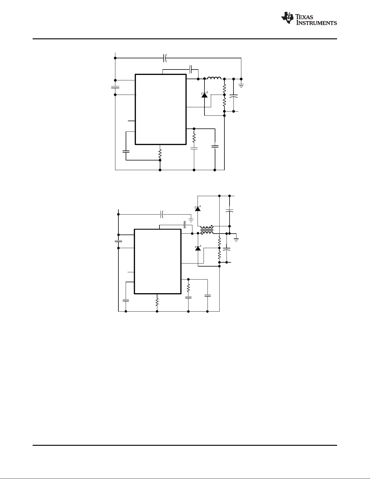
PH
VIN
GND
BOOT
VSENSE
COMP
TPS54240
EN
RT/CLK
SS/TR
Cpole
Czero
Rcomp
RT
Css
Co
Lo
Cboot
Cin
R1
R2
Cd
VIN
VOUT
+
+
GND
PH
VIN
GND
BOOT
VSENSE
COMP
TPS54240
EN
RT/CLK
SS/TR
Cpole
Czero
Rcomp
RT
Css
Coneg
Lo
Cboot
Cin
R1
R2
Cd
VIN
VONEG
+
+
GND
VOPOS
Copos
+
TPS54240
SLVSAA6 –APRIL 2010
Figure 63. TPS54240 Inverting Power Supply from SLVA317 Application Note
www.ti.com
Figure 64. TPS54240 Split Rail Power Supply Based on SLVA369 Application Note
40 Submit Documentation Feedback Copyright © 2010, Texas Instruments Incorporated
Product Folder Link(s): TPS54240
Page 41

TPS54240DGQ
TPS54240DGQ
TPS54240
www.ti.com
SLVSAA6 –APRIL 2010
Figure 65. 12V to 3.8V GSM Power Supply
Figure 66. 24V to 4.2V GSM Power Supply
Copyright © 2010, Texas Instruments Incorporated Submit Documentation Feedback 41
Product Folder Link(s): TPS54240
Page 42

PACKAGE OPTION ADDENDUM
www.ti.com 19-May-2010
PACKAGING INFORMATION
Orderable Device Status
(1)
Package
Type
TPS54240DGQ ACTIVE MSOP-
Power
Package
Drawing
Pins Package
Qty
Eco Plan
DGQ 10 80 Green (RoHS &
no Sb/Br)
(2)
Lead/Ball Finish MSL Peak Temp
CU NIPDAU Level-1-260C-UNLIM
(3)
PAD
TPS54240DGQR ACTIVE MSOP-
Power
DGQ 10 2500 Green (RoHS &
no Sb/Br)
CU NIPDAU Level-1-260C-UNLIM
PAD
TPS54240EVM-605 PREVIEW 0 1 TBD Call TI Call TI
(1)
The marketing status values are defined as follows:
ACTIVE: Product device recommended for new designs.
LIFEBUY: TI has announced that the device will be discontinued, and a lifetime-buy period is in effect.
NRND: Not recommended for new designs. Device is in production to support existing customers, but TI does not recommend using this part in
a new design.
PREVIEW: Device has been announced but is not in production. Samples may or may not be available.
OBSOLETE: TI has discontinued the production of the device.
(2)
Eco Plan - The planned eco-friendly classification: Pb-Free (RoHS), Pb-Free (RoHS Exempt), or Green (RoHS & no Sb/Br) - please check
http://www.ti.com/productcontent for the latest availability information and additional product content details.
TBD: The Pb-Free/Green conversion plan has not been defined.
Pb-Free (RoHS): TI's terms "Lead-Free" or "Pb-Free" mean semiconductor products that are compatible with the current RoHS requirements
for all 6 substances, including the requirement that lead not exceed 0.1% by weight in homogeneous materials. Where designed to be soldered
at high temperatures, TI Pb-Free products are suitable for use in specified lead-free processes.
Pb-Free (RoHS Exempt): This component has a RoHS exemption for either 1) lead-based flip-chip solder bumps used between the die and
package, or 2) lead-based die adhesive used between the die and leadframe. The component is otherwise considered Pb-Free (RoHS
compatible) as defined above.
Green (RoHS & no Sb/Br): TI defines "Green" to mean Pb-Free (RoHS compatible), and free of Bromine (Br) and Antimony (Sb) based flame
retardants (Br or Sb do not exceed 0.1% by weight in homogeneous material)
(3)
MSL, Peak Temp. -- The Moisture Sensitivity Level rating according to the JEDEC industry standard classifications, and peak solder
temperature.
Important Information and Disclaimer:The information provided on this page represents TI's knowledge and belief as of the date that it is
provided. TI bases its knowledge and belief on information provided by third parties, and makes no representation or warranty as to the
accuracy of such information. Efforts are underway to better integrate information from third parties. TI has taken and continues to take
reasonable steps to provide representative and accurate information but may not have conducted destructive testing or chemical analysis on
incoming materials and chemicals. TI and TI suppliers consider certain information to be proprietary, and thus CAS numbers and other limited
information may not be available for release.
In no event shall TI's liability arising out of such information exceed the total purchase price of the TI part(s) at issue in this document sold by TI
to Customer on an annual basis.
Addendum-Page 1
Page 43

PACKAGE MATERIALS INFORMATION
www.ti.com 20-Jul-2010
TAPE AND REEL INFORMATION
*All dimensions are nominal
Device Package
TPS54240DGQR MSOP-
Type
Power
PAD
Package
Drawing
DGQ 10 2500 330.0 12.4 5.3 3.3 1.3 8.0 12.0 Q1
Pins SPQ Reel
Diameter
(mm)
Reel
Width
W1 (mm)
A0
(mm)B0(mm)K0(mm)P1(mm)W(mm)
Quadrant
Pin1
Pack Materials-Page 1
Page 44

PACKAGE MATERIALS INFORMATION
www.ti.com 20-Jul-2010
*All dimensions are nominal
Device Package Type Package Drawing Pins SPQ Length (mm) Width (mm) Height (mm)
TPS54240DGQR MSOP-PowerPAD DGQ 10 2500 346.0 346.0 35.0
Pack Materials-Page 2
Page 45

Page 46

Page 47

Page 48

IMPORTANT NOTICE
Texas Instruments Incorporated and its subsidiaries (TI) reserve the right to make corrections, modifications, enhancements, improvements,
and other changes to its products and services at any time and to discontinue any product or service without notice. Customers should
obtain the latest relevant information before placing orders and should verify that such information is current and complete. All products are
sold subject to TI’s terms and conditions of sale supplied at the time of order acknowledgment.
TI warrants performance of its hardware products to the specifications applicable at the time of sale in accordance with TI’s standard
warranty. Testing and other quality control techniques are used to the extent TI deems necessary to support this warranty. Except where
mandated by government requirements, testing of all parameters of each product is not necessarily performed.
TI assumes no liability for applications assistance or customer product design. Customers are responsible for their products and
applications using TI components. To minimize the risks associated with customer products and applications, customers should provide
adequate design and operating safeguards.
TI does not warrant or represent that any license, either express or implied, is granted under any TI patent right, copyright, mask work right,
or other TI intellectual property right relating to any combination, machine, or process in which TI products or services are used. Information
published by TI regarding third-party products or services does not constitute a license from TI to use such products or services or a
warranty or endorsement thereof. Use of such information may require a license from a third party under the patents or other intellectual
property of the third party, or a license from TI under the patents or other intellectual property of TI.
Reproduction of TI information in TI data books or data sheets is permissible only if reproduction is without alteration and is accompanied
by all associated warranties, conditions, limitations, and notices. Reproduction of this information with alteration is an unfair and deceptive
business practice. TI is not responsible or liable for such altered documentation. Information of third parties may be subject to additional
restrictions.
Resale of TI products or services with statements different from or beyond the parameters stated by TI for that product or service voids all
express and any implied warranties for the associated TI product or service and is an unfair and deceptive business practice. TI is not
responsible or liable for any such statements.
TI products are not authorized for use in safety-critical applications (such as life support) where a failure of the TI product would reasonably
be expected to cause severe personal injury or death, unless officers of the parties have executed an agreement specifically governing
such use. Buyers represent that they have all necessary expertise in the safety and regulatory ramifications of their applications, and
acknowledge and agree that they are solely responsible for all legal, regulatory and safety-related requirements concerning their products
and any use of TI products in such safety-critical applications, notwithstanding any applications-related information or support that may be
provided by TI. Further, Buyers must fully indemnify TI and its representatives against any damages arising out of the use of TI products in
such safety-critical applications.
TI products are neither designed nor intended for use in military/aerospace applications or environments unless the TI products are
specifically designated by TI as military-grade or "enhanced plastic." Only products designated by TI as military-grade meet military
specifications. Buyers acknowledge and agree that any such use of TI products which TI has not designated as military-grade is solely at
the Buyer's risk, and that they are solely responsible for compliance with all legal and regulatory requirements in connection with such use.
TI products are neither designed nor intended for use in automotive applications or environments unless the specific TI products are
designated by TI as compliant with ISO/TS 16949 requirements. Buyers acknowledge and agree that, if they use any non-designated
products in automotive applications, TI will not be responsible for any failure to meet such requirements.
Following are URLs where you can obtain information on other Texas Instruments products and application solutions:
Products Applications
Amplifiers amplifier.ti.com Audio www.ti.com/audio
Data Converters dataconverter.ti.com Automotive www.ti.com/automotive
DLP® Products www.dlp.com Communications and www.ti.com/communications
DSP dsp.ti.com Computers and www.ti.com/computers
Clocks and Timers www.ti.com/clocks Consumer Electronics www.ti.com/consumer-apps
Interface interface.ti.com Energy www.ti.com/energy
Logic logic.ti.com Industrial www.ti.com/industrial
Power Mgmt power.ti.com Medical www.ti.com/medical
Microcontrollers microcontroller.ti.com Security www.ti.com/security
RFID www.ti-rfid.com Space, Avionics & www.ti.com/space-avionics-defense
RF/IF and ZigBee® Solutions www.ti.com/lprf Video and Imaging www.ti.com/video
Mailing Address: Texas Instruments, Post Office Box 655303, Dallas, Texas 75265
Copyright © 2010, Texas Instruments Incorporated
Telecom
Peripherals
Defense
Wireless www.ti.com/wireless-apps
 Loading...