

Page 1

User's Guide
SLVU331 – September 2009
TPS54218EVM-511 2-A, SWIFT™ Regulator Evaluation
Module
Contents
1 Introduction ................................................................................................................... 2
2 Test Setup and Results ..................................................................................................... 4
3 Board Layout ................................................................................................................ 10
4 Schematic and Bill of Materials ........................................................................................... 14
List of Figures
1 TPS54218EVM-511 Efficiency ............................................................................................. 5
2 TPS54218EVM-511 Low Current Efficiency ............................................................................. 5
3 TPS54218EVM-511 Load Regulation ..................................................................................... 6
4 TPS54218EVM-511 Line Regulation ...................................................................................... 6
5 TPS54218EVM-511 Transient Response ............................................................................... 7
6 TPS54218EVM-511 Loop Response ..................................................................................... 7
7 TPS54218EVM-511 Output Ripple ....................................................................................... 8
8 TPS54218EVM-511 Input Ripple ......................................................................................... 8
9 TPS54218EVM-511 Start-Up Relative to V
10 TPS54218EVM-511 Start-up Relative to Enable ....................................................................... 9
11 TPS54218EVM-511 Top-Side Layout ................................................................................... 10
12 TPS54218EVM-511 Bottom-Side Layout ............................................................................... 11
13 TPS54218EVM-511 Layout 2 ............................................................................................. 12
14 TPS54218EVM-511 Layout 3 ............................................................................................. 13
15 TPS54218EVM-511 Top-Side Assembly................................................................................ 14
16 TPS54218EVM-511 Schematic .......................................................................................... 15
............................................................................ 9
IN
1 Input Voltage and Output Current Summary ............................................................................. 2
2 TPS54218EVM-511 Performance Specification Summary ............................................................. 2
3 Output Voltages Available .................................................................................................. 3
4 EVM Connectors and Test Points ......................................................................................... 4
5 TPS54218EVM-511 Bill of Materials ..................................................................................... 16
SWIFT is a trademark of Texas Instruments.
SLVU331 – September 2009 TPS54218EVM-511 2-A, SWIFT™ Regulator Evaluation Module 1
Submit Documentation Feedback
List of Tables
Page 2
Introduction
www.ti.com
1 Introduction
This user's guide contains background information for the TPS54218 as well as support documentation for
the TPS54218EVM-511 evaluation module (HPA375). Also included are the performance specifications,
the schematic, and the bill of materials for the TPS54218EVM-511.
1.1 Background
The TPS54218 dc/dc converter is designed to provide up to a 2 A output from an input voltage source of
2.95 V to 6 V. Rated input voltage and output current range for the evaluation module are given in
Table 1 . This evaluation module is designed to demonstrate the small printed-circuit-board areas that may
be achieved when designing with the TPS54218 regulator. The switching frequency is externally set at a
nominal 1000 kHz. The high-side and low-side MOSFETs are incorporated inside the TPS54218 package
along with the gate drive circuitry. The low drain-to-source on resistance of the MOSFETs allow the
TPS54218 to achieve high efficiencies and helps keep the junction temperature low at high output
currents. The compensation components are external to the integrated circuit (IC), and an external divider
allows for an adjustable output voltage. Additionally, the TPS54218 provides adjustable slow start and
undervoltage lockout inputs. The absolute maximum input voltage is 7 V for the TPS54218EVM-511.
Table 1. Input Voltage and Output Current Summary
EVM INPUT VOLTAGE RANGE OUTPUT CURRENT RANGE
TPS54218EVM-511 VIN = 3 V to 6 V (VIN start = 3.1 V) 0 A to 2 A
1.2 Performance Specification Summary
A summary of the TPS54218EVM-511 performance specifications is provided in Table 2 . Specifications
are given for an input voltage of V
The TPS54218EVM-511 is designed and tested for V
all measurements, unless otherwise noted.
Table 2. TPS54218EVM-511 Performance Specification Summary
SPECIFICATION TEST CONDITIONS MIN TYP MAX UNIT
VINoperating voltage range 3 3.3 6 V
VINstart voltage 3.1 V
VINstop voltage 2.8 V
Output voltage set point 1.8 V
Output current range VIN= 3 V to 6 V 0 2 A
Line regulation IO= 1 A, VIN= 3 V to 6 V ± 0.06%
Load regulation VIN= 3.3 V, IO= 0 A to 2 A ± 0.04%
Load transient response
Loop bandwidth VIN= 3.3 V, IO= 2 A 45 kHz
Phase margin VIN= 3.3 V , IO= 2 A 58 °
Input ripple voltage IO= 2 A 100 mV
Output ripple voltage IO= 2 A 5 mV
Output rise time 4 ms
Operating frequency 1000 kHz
Maximum efficiency TPS54218EVM-511, VIN= 3.3 V, IO= 0.4 A 94.5%
= 3.3 V and an output voltage of 1.8 V, unless otherwise specified.
IN
IO= 0.5 A to 1.5 A
IO= 1.5 A to 0.5 A
= 3 V to 6 V. The ambient temperature is 25 ° C for
IN
Voltage change –20 mV
Recovery time 400 µ s
Voltage change 20 mV
Recovery time 400 µ s
PP
PP
TPS54218EVM-511 2-A, SWIFT™ Regulator Evaluation Module2 SLVU331 – September 2009
Submit Documentation Feedback
Page 3
OUT
0.8 V
R7 = 100 kΩ ×
V - 0.8 V
Tss(mS) Iss( A)
C7(nF) =
Vref(V)
´ m
-
× -
´
START STOP
6
0.944 V V
R1 =
2.59 10
-
×
- + × ´
6
ST OP
1.18 R1
R2 =
V 1.1 8 R1 3 .2 1 0
www.ti.com
1.3 Modifications
These evaluation modules are designed to provide access to the features of the TPS54218. Some
modifications can be made to this module.
1.3.1 Output Voltage Set Point
The voltage divider R6 and R7 is used to set the output voltage. To change the output voltage of the EVM,
it is necessary to change the value of resistor R7. Changing the value of R7 can change the output
voltage above 0.8 V. The value of R7 for a specific output voltage can be calculated using Equation 1 .
Table 3 lists the R7 values for some common output voltages. Note that V
minimum on-time is greater than 80 ns, and the maximum duty cycle is less than 92%. The values given
in Table 3 are standard values, not the exact value calculated using Equation 1 .
Table 3. Output Voltages Available
Output Voltage (V) R7 Value (k Ω )
1.0 402
1.2 200
1.5 115
1.8 80.6
2.5 47.5
must be in a range so that the
IN
Introduction
(1)
1.3.2 Slow Start Time
The slow start time can be adjusted by changing the value of C7. Use Equation 2 to calculate the required
value of C7 for a desired slow start time
C7 is set to 0.01 µ F on the EVM for a default slowstart time of 4 msec.
1.3.3 Adjustable UVLO
The undervoltage lock out (UVLO) can be adjusted externally using R1 and R2. The EVM is set for a start
voltage of 3.1 V and a stop voltage of 2.8 V using R1 = 48.8 k Ω and R2 = 32.4 k Ω . Use Equation 3 and
Equation 4 to calculate required resistor values for different start and stop voltages.
(2)
(3)
(4)
SLVU331 – September 2009 TPS54218EVM-511 2-A, SWIFT™ Regulator Evaluation Module 3
Submit Documentation Feedback
Page 4
Test Setup and Results
2 Test Setup and Results
This section describes how to properly connect, set up, and use the TPS54218EVM-511 evaluation
module. The section also includes test results typical for the evaluation module and covers efficiency,
output voltage regulation, load transients, loop response, output ripple, input ripple, and start-up.
2.1 Input / Output Connections
The TPS54218EVM-511 is provided with input/output connectors and test points as shown in Table 4 . A
power supply capable of supplying 2 A must be connected to J1 through a pair of 20 AWG wires. The load
must be connected to J4 through a pair of 20 AWG wires. The maximum load current capability must be at
least 2 A to use the full capability of this EVM. Wire lengths must be minimized to reduce losses in the
wires. Test-point TP1 provides a place to monitor the V
ground reference. TP6 is used to monitor the output voltage with TP7 as the ground reference.
Reference Designator Function
input voltages with TP2 providing a convenient
IN
Table 4. EVM Connectors and Test Points
J1 VIN(see Table 1 for VINrange).
J2 2-pin header for enable. Connect EN to ground to disable, open to enable.
J3 2-pin header for to allow pull up of PWRGD to VIN.
J4 V
TP1 VINtest point at VINconnector.
TP2 GND test point at VIN.
TP3 PH test point
TP4 Slow start monitor test point.
TP5 Test point between voltage divider network and output. Used for loop response measurements.
TP6 Output voltage test point at OUT connector.
TP7 GND test point at OUT connector.
, 1.8 V at 4 A maximum.
OUT
www.ti.com
4 TPS54218EVM-511 2-A, SWIFT™ Regulator Evaluation Module SLVU331 – September 2009
Submit Documentation Feedback
Page 5
50
55
60
65
70
75
80
85
90
95
100
0 0.25 0.5 0.75 1 1.25 1.5 1.75 2
I -OutputCurrent- A
O
Efficiency-%
V =3.3V
I
V =5V
I
0
10
20
30
40
50
60
70
80
90
100
0.001 0.01 0.1 1 10
I -OutputCurrent- A
O
Efficiency-%
V =3.3V
I
Vin=5V
www.ti.com
Test Setup and Results
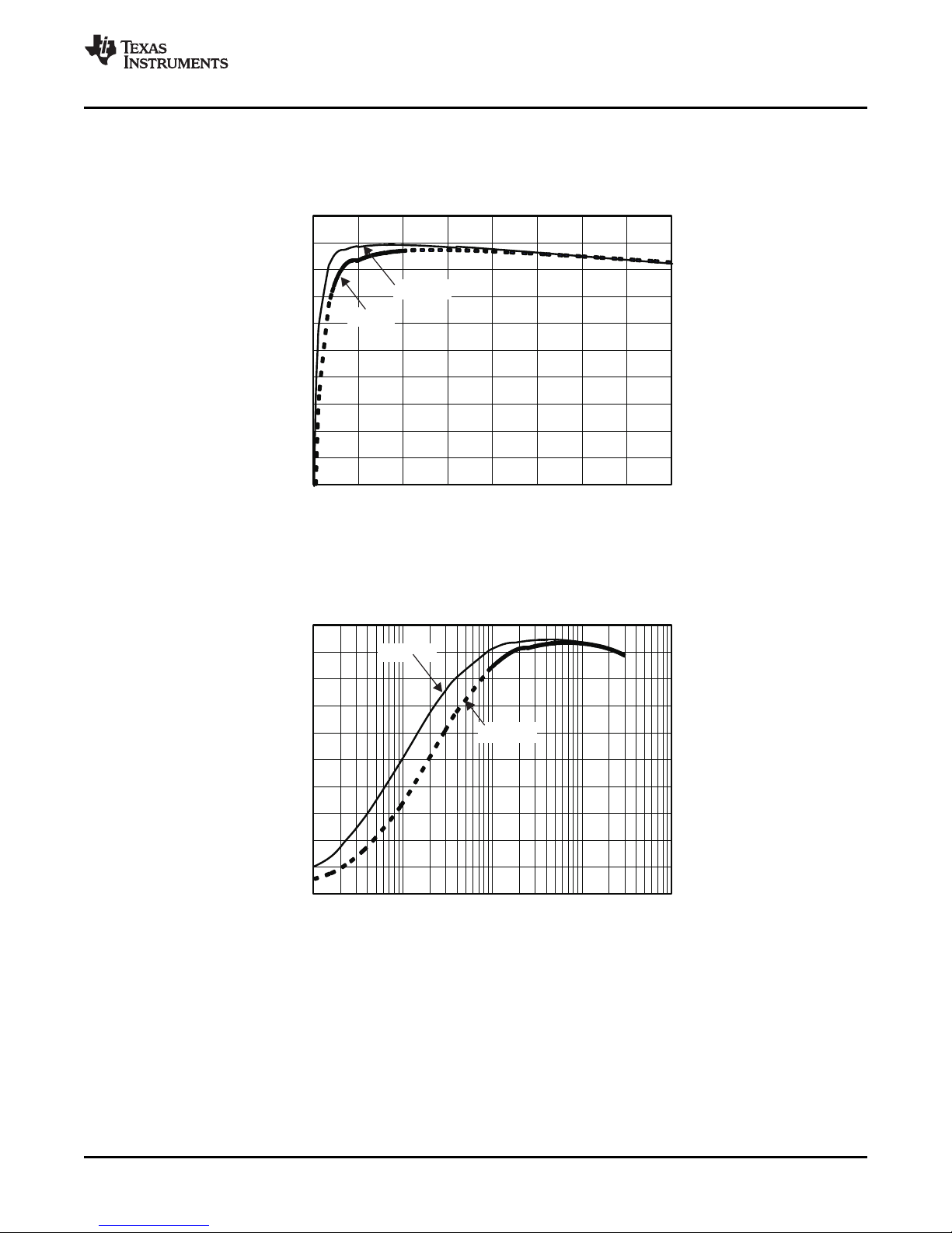
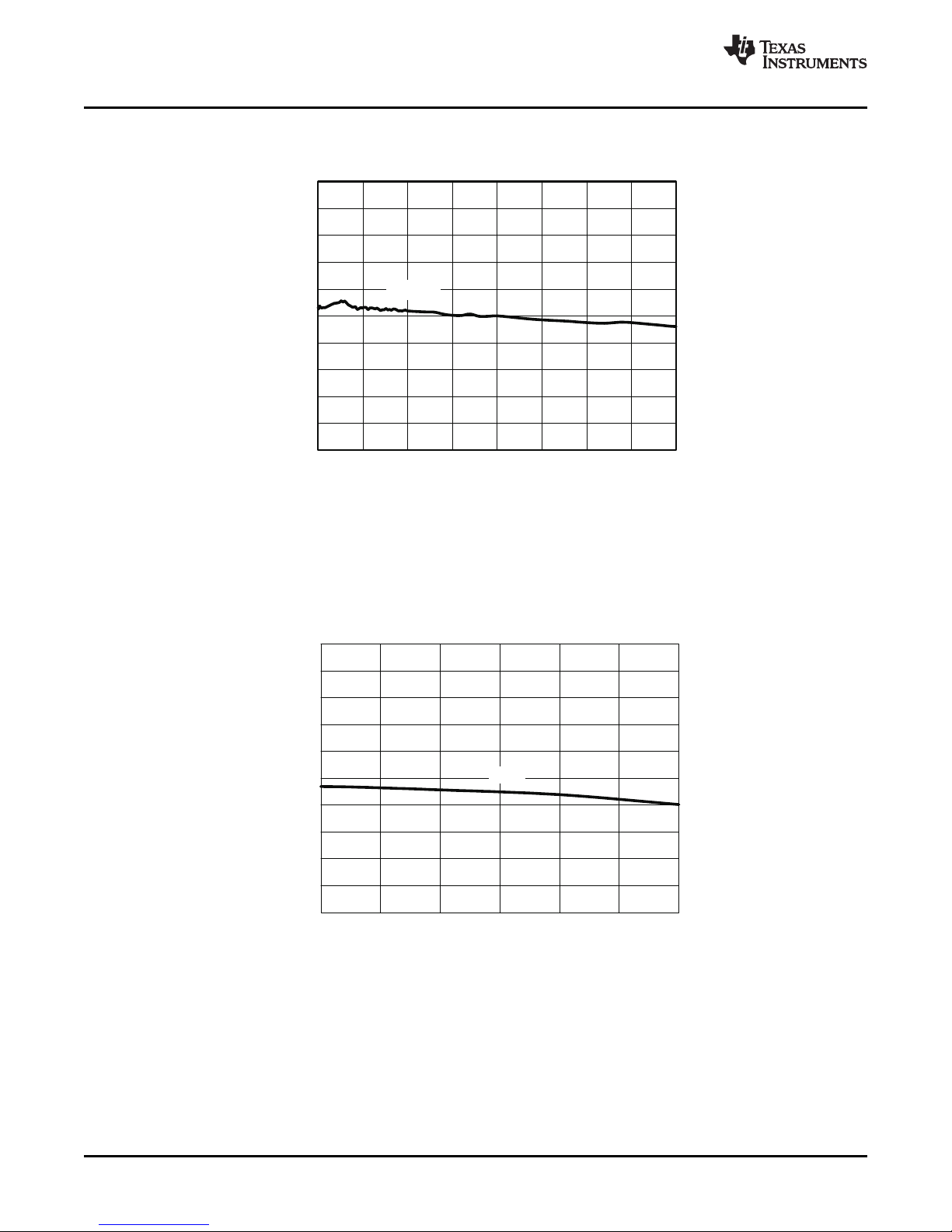
2.2 Efficiency
The efficiency of this EVM peaks at a load current of about 0.4 A – 0.7 A and then decreases as the load
current increases towards full load. Figure 1 shows the efficiency for the TPS54218EVM-511 at an
ambient temperature of 25 ° C.
Figure 1. TPS54218EVM-511 Efficiency
Figure 2 shows the efficiency for the TPS54218EVM-511 at lower output currents on a semi log scale at
an ambient temperature of 25 ° C.
Figure 2. TPS54218EVM-511 Low Current Efficiency
The efficiency may be lower at higher ambient temperatures, due to temperature variation in the
drain-to-source resistance of the internal MOSFET.
SLVU331 – September 2009 TPS54218EVM-511 2-A, SWIFT™ Regulator Evaluation Module 5
Submit Documentation Feedback
Page 6
-0.25
-0.2
-0.15
-0.1
-0.05
0
0.05
0.1
0.15
0.2
0.25
0 0.25 0.5 0.75 1 1.25 1.5 1.75 2
I -OutputCurrent- A
O
OutputVoltageChange-%
V =3.3V
I
1.79
1.792
1.794
1.796
1.798
1.8
1.802
1.804
1.806
1.808
1.81
3 3.5 4 4.5 5 5.5 6
V -InputVoltage-V
I
V -OutputVoltage-V
O
I =1
O
Test Setup and Results
2.3 Output Voltage Load Regulation
Figure 3 shows the load regulation for the TPS54218EVM-511.
Measurements are given for an ambient temperature of 25 ° C.
www.ti.com
Figure 3. TPS54218EVM-511 Load Regulation
2.4 Output Voltage Line Regulation
Figure 4 shows the line regulation for the TPS54218EVM-511.
TPS54218EVM-511 2-A, SWIFT™ Regulator Evaluation Module6 SLVU331 – September 2009
Figure 4. TPS54218EVM-511 Line Regulation
Submit Documentation Feedback
Page 7

V =50mV/div(accoupled)
OUT
I =1 A/div,
0.5to1.5 A step
OUT
Time=2ms/div
60
-60
Gain
10 1M
f-Frequency-Hz
Phase
180
-180
Gain
Fhase
www.ti.com
Test Setup and Results
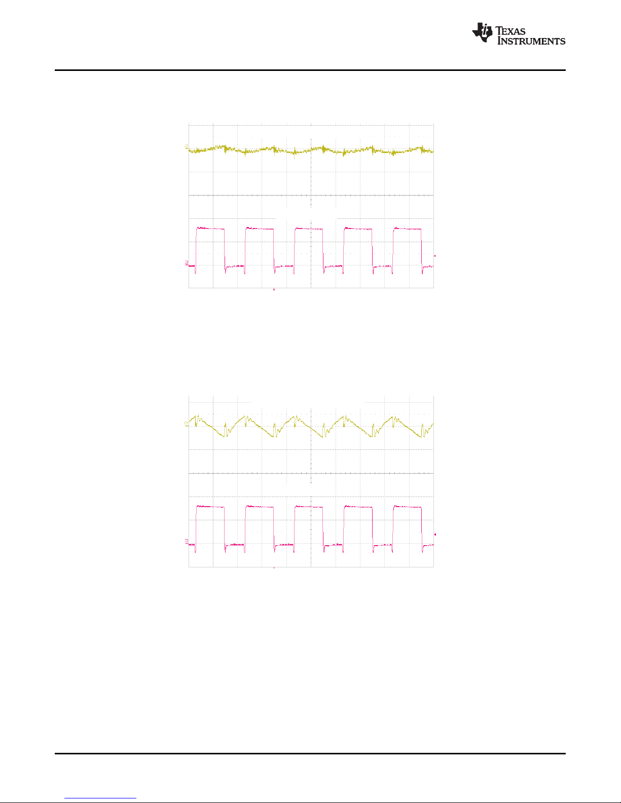
2.5 Load Transients
Figure 5 shows the TPS54318EVM-375 response to load transients. The current step is from 25% to 75%
of maximum rated load at 3.3 V input. Total peak-to-peak voltage variation is as shown, including ripple
and noise on the output.
Figure 5. TPS54218EVM-511 Transient Response
2.6 Loop Characteristics
Figure 6 shows the TPS54218EVM-511 loop-response characteristics. Gain and phase plots are shown
for V
voltage of 3.3 V. Load current for the measurement is 2 A.
IN
Figure 6. TPS54218EVM-511 Loop Response
SLVU331 – September 2009 TPS54218EVM-511 2-A, SWIFT™ Regulator Evaluation Module 7
Submit Documentation Feedback
Page 8
V =10mV/div(accoupled)
OUT
PH=2V/div
Time=500ns/div
V =50mV/div(accoupled)
I
PH=2V/div
Time=500ns/div
Test Setup and Results
2.7 Output Voltage Ripple
Figure 7 shows the TPS54218EVM-511 output voltage ripple. The output current is the rated full load of
2 A and V
2.8 Input Voltage Ripple
Figure 8 shows the TPS54218EVM-511 input voltage ripple. The output current is the rated full load of
2 A and V
= 3.3 V. The ripple voltage is measured directly across the output capacitors.
IN
Figure 7. TPS54218EVM-511 Output Ripple
= 3.3 V. The ripple voltage is measured directly across the input capacitors.
IN
www.ti.com
TPS54218EVM-511 2-A, SWIFT™ Regulator Evaluation Module8 SLVU331 – September 2009
Figure 8. TPS54218EVM-511 Input Ripple
Submit Documentation Feedback
Page 9

V =2V/div
I
EN=1V/div
SS=1V/div
V =1V/div
O
Time=5ms/div
V =2V/div
I
EN=1V/div
SS=1V/div
V =1V/div
O
Time=5ms/div
www.ti.com
2.9 Powering Up
Figure 9 and Figure 10 show the start-up waveforms for the TPS54218EVM-511. In Figure 9 , the output
voltage ramps up as soon as the input voltage reaches the UVLO threshold as set by the R
resistor divider network. In Figure 10 , the input voltage is initially applied and the output is inhibited by
using a jumper at J2 to tie EN to GND. When the jumper is removed, EN is released. When the EN
voltage reaches the enable-threshold voltage, the start-up sequence begins and the output voltage ramps
up to the externally set value of 1.8 V. The input voltage for these plots is 5 V and the load is 1 Ω .
Test Setup and Results
and R
1
2
Figure 9. TPS54218EVM-511 Start-Up Relative to V
Figure 10. TPS54218EVM-511 Start-up Relative to Enable
IN
SLVU331 – September 2009 TPS54218EVM-511 2-A, SWIFT™ Regulator Evaluation Module 9
Submit Documentation Feedback
Page 10
Board Layout
3 Board Layout
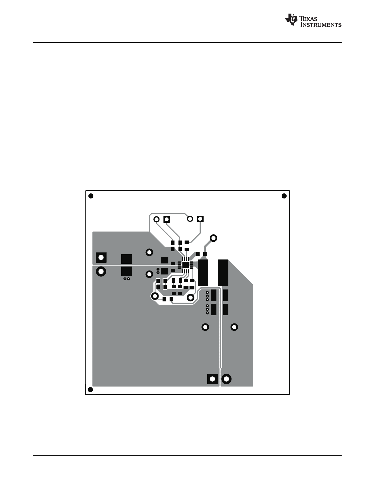
3.1 Layout
www.ti.com
This section provides a description of the TPS54218EVM-511, board layout, and layer illustrations.
Figure 11 through Figure 15 shows the board layout for the TPS54218EVM-511. The topside layer of the
EVM is laid out in a manner typical of a user application. The top, bottom and internal layers are 2-oz.
copper.
The top layer contains the main power traces for V
, V
IN
, and VPHASE. Also on the top layer are
OUT
connections for the remaining pins of the TPS54218 and a large area filled with ground. The bottom and
internal layers contain ground planes only. The top-side ground areas are connected to the bottom and
internal ground planes with multiple vias placed around the board including four vias directly under the
TPS54218 device to provide a thermal path from the top-side ground area to the bottom-side and internal
ground planes.
The input decoupling capacitors (C2, and C3) and bootstrap capacitor (C6) are all located as close to the
IC as possible. In addition, the voltage set-point resistor divider components are also kept close to the IC.
The voltage divider network ties to the output voltage at the point of regulation, the copper V
trace near
OUT
the output connector J4. For the TPS54218, an additional input bulk capacitor may be required, depending
on the EVM connection to the input supply.
Figure 11. TPS54218EVM-511 Top-Side Layout
10 TPS54218EVM-511 2-A, SWIFT™ Regulator Evaluation Module SLVU331 – September 2009
Submit Documentation Feedback
Page 11
www.ti.com
Board Layout
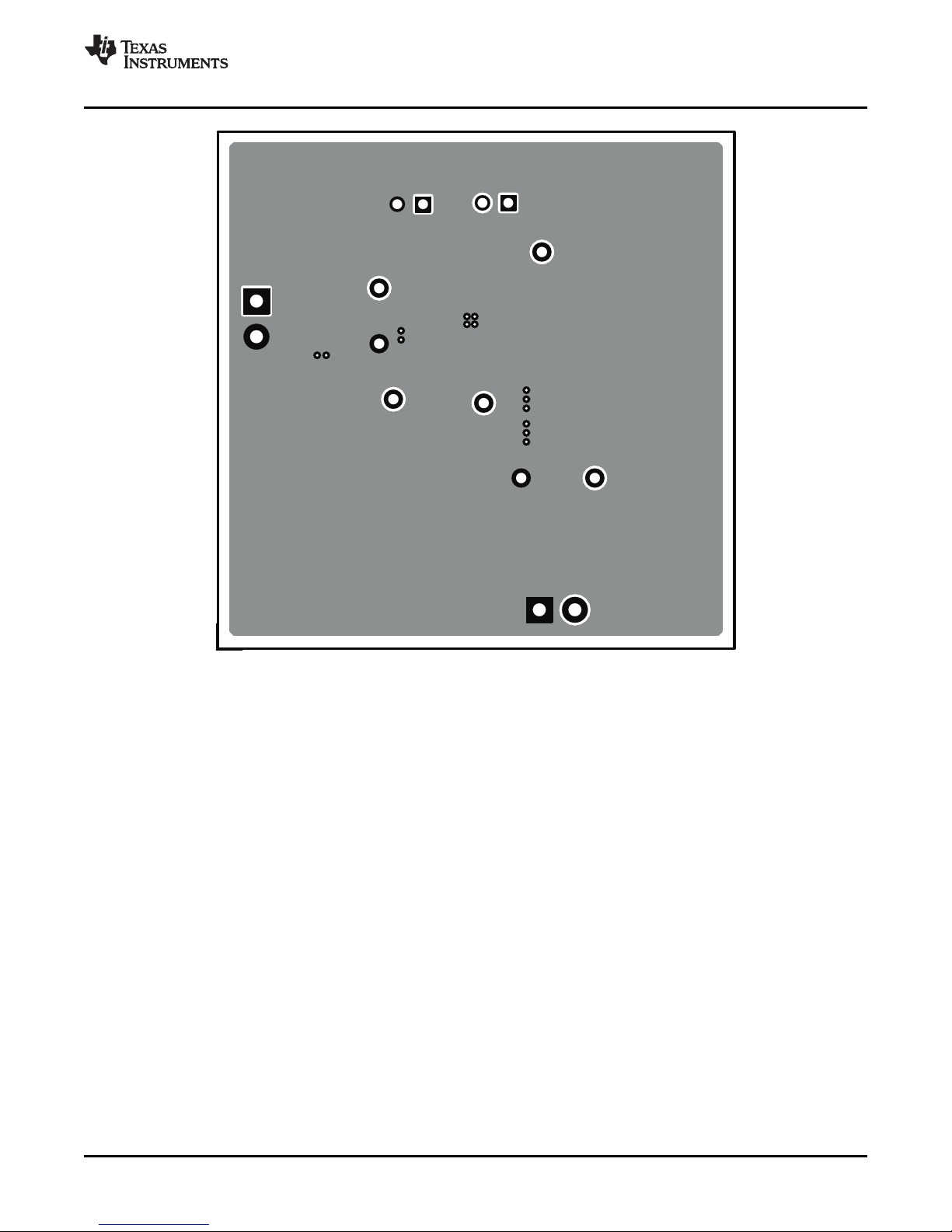
Figure 12. TPS54218EVM-511 Bottom-Side Layout
SLVU331 – September 2009 TPS54218EVM-511 2-A, SWIFT™ Regulator Evaluation Module 11
Submit Documentation Feedback
Page 12

Board Layout
www.ti.com
Figure 13. TPS54218EVM-511 Layout 2
TPS54218EVM-511 2-A, SWIFT™ Regulator Evaluation Module12 SLVU331 – September 2009
Submit Documentation Feedback
Page 13

www.ti.com
Board Layout
Figure 14. TPS54218EVM-511 Layout 3
SLVU331 – September 2009 TPS54218EVM-511 2-A, SWIFT™ Regulator Evaluation Module 13
Submit Documentation Feedback
Page 14

Schematic and Bill of Materials
www.ti.com
3.2 Estimated Circuit Area
The estimated printed circuit board area for the components used in this design is 0.37 in
This area does not include test point or connectors.
4 Schematic and Bill of Materials
This section presents the TPS54218EVM-511 schematic and bill of materials.
Figure 15. TPS54218EVM-511 Top-Side Assembly
2
(239 mm
2
).
14 TPS54218EVM-511 2-A, SWIFT™ Regulator Evaluation Module SLVU331 – September 2009
Submit Documentation Feedback
Page 15

www.ti.com
Schematic and Bill of Materials
4.1 Schematic
Figure 16 is the schematic for the TPS54218EVM-511.
SLVU331 – September 2009 TPS54218EVM-511 2-A, SWIFT™ Regulator Evaluation Module 15
Submit Documentation Feedback
Figure 16. TPS54218EVM-511 Schematic
Page 16

Schematic and Bill of Materials
4.2 Bill of Materials
Table 5 presents the bill of materials for the TPS54218EVM-511.
Table 5. TPS54218EVM-511 Bill of Materials
COUNT RefDes Value Description Size Part Number MFR
0 C1 Open Capacitor, Ceramic Multi sizes Engineering Only Std
1 C2 10uF Capacitor, Ceramic, 10V, X5R, 1206 Std Std
20%
2 C3, C6 0.1uF Capacitor, Ceramic, 25V, X5R, 0603 Std Std
10%
1 C4 3900pF Capacitor, Ceramic, 50V, X5R, 0603 Std Std
10%
0 C5 Open Capacitor, Ceramic 0603 Std Std
1 C7 0.01uF Capacitor, Ceramic, 16V, X7R, 0603 Std Std
10%
2 C8, C9 22 uF Capacitor, Ceramic, 10V, X5R, 1210 Std Std
20%
2 J1, J4 ED555/2DS Terminal Block, 2-pin, 6-A, 0.27 x 0.25 inch ED555/2DS OST
3.5mm
2 J2, J3 PEC02SAAN Header, Male 2-pin, 100mil 0.100 inch x 2 PEC02SAAN Sullins
spacing
1 L1 2.2 uH INDUCTOR, Power 0.276 x 0.276 inch XPL7030-222ML Coilcraft
1 R1 32.4k Resistor, Chip, 1/16W, 1% 0603 Std Std
1 R2 48.7k Resistor, Chip, 1/16W, 1% 0603 Std Std
1 R3 9.53k Resistor, Chip, 1/16W, 1% 0603 Std Std
2 R4, R6 100k Resistor, Chip, 1/16W, 1% 0603 Std Std
1 R5 182k Resistor, Chip, 1/16W, 1% 0603 Std Std
1 R7 80.6k Resistor, Chip, 1/16W, 1% 0603 Std Std
1 R8 51.1 Resistor, Chip, 1/16W, 1% 0603 Std Std
5 TP1, TP3 - TP6 5000 Test Point, Red, Thru Hole Color 0.100 x 0.100 inch 5000 Keystone
Keyed
2 TP2, TP7 5001 Test Point, Black, Thru Hole 0.100 x 0.100 inch 5001 Keystone
Color Keyed
1 U1 TPS54218RTE IC, DC-DC Converter, 3-6 V, 2A QFN-16 TPS54218RTE TI
2 -- Shunt, 100-mil, Black 0.100 929950-00
1 -- PCB, 2.0" x 2.0" x 0.062" HPA511
Notes: 1. These assemblies are ESD sensitive, ESD precautions shall be observed.
2. These assemblies must be clean and free from flux and all contaminants. Use of no clean flux is not acceptable.
3. These assemblies must comply with workmanship standards IPC-A-610 Class 2.
4. Ref designators marked with an asterisk ('**') cannot be substituted. All other components can be substituted with equivalent
aaMFG's components.
www.ti.com
TPS54218EVM-511 2-A, SWIFT™ Regulator Evaluation Module16 SLVU331 – September 2009
Submit Documentation Feedback
Page 17

EVALUATION BOARD/KIT IMPORTANT NOTICE
Texas Instruments (TI) provides the enclosed product(s) under the following conditions:
This evaluation board/kit is intended for use for ENGINEERING DEVELOPMENT, DEMONSTRATION, OR EVALUATION PURPOSES
ONLY and is not considered by TI to be a finished end-product fit for general consumer use. Persons handling the product(s) must have
electronics training and observe good engineering practice standards. As such, the goods being provided are not intended to be complete
in terms of required design-, marketing-, and/or manufacturing-related protective considerations, including product safety and environmental
measures typically found in end products that incorporate such semiconductor components or circuit boards. This evaluation board/kit does
not fall within the scope of the European Union directives regarding electromagnetic compatibility, restricted substances (RoHS), recycling
(WEEE), FCC, CE or UL, and therefore may not meet the technical requirements of these directives or other related directives.
Should this evaluation board/kit not meet the specifications indicated in the User’s Guide, the board/kit may be returned within 30 days from
the date of delivery for a full refund. THE FOREGOING WARRANTY IS THE EXCLUSIVE WARRANTY MADE BY SELLER TO BUYER
AND IS IN LIEU OF ALL OTHER WARRANTIES, EXPRESSED, IMPLIED, OR STATUTORY, INCLUDING ANY WARRANTY OF
MERCHANTABILITY OR FITNESS FOR ANY PARTICULAR PURPOSE.
The user assumes all responsibility and liability for proper and safe handling of the goods. Further, the user indemnifies TI from all claims
arising from the handling or use of the goods. Due to the open construction of the product, it is the user’s responsibility to take any and all
appropriate precautions with regard to electrostatic discharge.
EXCEPT TO THE EXTENT OF THE INDEMNITY SET FORTH ABOVE, NEITHER PARTY SHALL BE LIABLE TO THE OTHER FOR ANY
INDIRECT, SPECIAL, INCIDENTAL, OR CONSEQUENTIAL DAMAGES.
TI currently deals with a variety of customers for products, and therefore our arrangement with the user is not exclusive.
TI assumes no liability for applications assistance, customer product design, software performance, or infringement of patents or
services described herein.
Please read the User’s Guide and, specifically, the Warnings and Restrictions notice in the User’s Guide prior to handling the product. This
notice contains important safety information about temperatures and voltages. For additional information on TI’s environmental and/or
safety programs, please contact the TI application engineer or visit www.ti.com/esh .
No license is granted under any patent right or other intellectual property right of TI covering or relating to any machine, process, or
combination in which such TI products or services might be or are used.
FCC Warning
This evaluation board/kit is intended for use for ENGINEERING DEVELOPMENT, DEMONSTRATION, OR EVALUATION PURPOSES
ONLY and is not considered by TI to be a finished end-product fit for general consumer use. It generates, uses, and can radiate radio
frequency energy and has not been tested for compliance with the limits of computing devices pursuant to part 15 of FCC rules, which are
designed to provide reasonable protection against radio frequency interference. Operation of this equipment in other environments may
cause interference with radio communications, in which case the user at his own expense will be required to take whatever measures may
be required to correct this interference.
EVM WARNINGS AND RESTRICTIONS
It is important to operate this EVM within the input voltage range and the output current range specified in Table 1.
Exceeding the specified input range may cause unexpected operation and/or irreversible damage to the EVM. If there are questions
concerning the input range, please contact a TI field representative prior to connecting the input power.
Applying loads outside of the specified output range may result in unintended operation and/or possible permanent damage to the EVM.
Please consult the EVM User's Guide prior to connecting any load to the EVM output. If there is uncertainty as to the load specification,
please contact a TI field representative.
During normal operation, some circuit components may have case temperatures greater than 55 ° C. The EVM is designed to operate
properly with certain components above 60 ° C as long as the input and output ranges are maintained. These components include but are
not limited to linear regulators, switching transistors, pass transistors, and current sense resistors. These types of devices can be identified
using the EVM schematic located in the EVM User's Guide. When placing measurement probes near these devices during operation,
please be aware that these devices may be very warm to the touch.
Mailing Address: Texas Instruments, Post Office Box 655303, Dallas, Texas 75265
Copyright 2006, Texas Instruments Incorporated
Page 18

IMPORTANT NOTICE
Texas Instruments Incorporated and its subsidiaries (TI) reserve the right to make corrections, modifications, enhancements, improvements,
and other changes to its products and services at any time and to discontinue any product or service without notice. Customers should
obtain the latest relevant information before placing orders and should verify that such information is current and complete. All products are
sold subject to TI’s terms and conditions of sale supplied at the time of order acknowledgment.
TI warrants performance of its hardware products to the specifications applicable at the time of sale in accordance with TI’s standard
warranty. Testing and other quality control techniques are used to the extent TI deems necessary to support this warranty. Except where
mandated by government requirements, testing of all parameters of each product is not necessarily performed.
TI assumes no liability for applications assistance or customer product design. Customers are responsible for their products and
applications using TI components. To minimize the risks associated with customer products and applications, customers should provide
adequate design and operating safeguards.
TI does not warrant or represent that any license, either express or implied, is granted under any TI patent right, copyright, mask work right,
or other TI intellectual property right relating to any combination, machine, or process in which TI products or services are used. Information
published by TI regarding third-party products or services does not constitute a license from TI to use such products or services or a
warranty or endorsement thereof. Use of such information may require a license from a third party under the patents or other intellectual
property of the third party, or a license from TI under the patents or other intellectual property of TI.
Reproduction of TI information in TI data books or data sheets is permissible only if reproduction is without alteration and is accompanied
by all associated warranties, conditions, limitations, and notices. Reproduction of this information with alteration is an unfair and deceptive
business practice. TI is not responsible or liable for such altered documentation. Information of third parties may be subject to additional
restrictions.
Resale of TI products or services with statements different from or beyond the parameters stated by TI for that product or service voids all
express and any implied warranties for the associated TI product or service and is an unfair and deceptive business practice. TI is not
responsible or liable for any such statements.
TI products are not authorized for use in safety-critical applications (such as life support) where a failure of the TI product would reasonably
be expected to cause severe personal injury or death, unless officers of the parties have executed an agreement specifically governing
such use. Buyers represent that they have all necessary expertise in the safety and regulatory ramifications of their applications, and
acknowledge and agree that they are solely responsible for all legal, regulatory and safety-related requirements concerning their products
and any use of TI products in such safety-critical applications, notwithstanding any applications-related information or support that may be
provided by TI. Further, Buyers must fully indemnify TI and its representatives against any damages arising out of the use of TI products in
such safety-critical applications.
TI products are neither designed nor intended for use in military/aerospace applications or environments unless the TI products are
specifically designated by TI as military-grade or "enhanced plastic." Only products designated by TI as military-grade meet military
specifications. Buyers acknowledge and agree that any such use of TI products which TI has not designated as military-grade is solely at
the Buyer's risk, and that they are solely responsible for compliance with all legal and regulatory requirements in connection with such use.
TI products are neither designed nor intended for use in automotive applications or environments unless the specific TI products are
designated by TI as compliant with ISO/TS 16949 requirements. Buyers acknowledge and agree that, if they use any non-designated
products in automotive applications, TI will not be responsible for any failure to meet such requirements.
Following are URLs where you can obtain information on other Texas Instruments products and application solutions:
Products Applications
Amplifiers amplifier.ti.com Audio www.ti.com/audio
Data Converters dataconverter.ti.com Automotive www.ti.com/automotive
DLP® Products www.dlp.com Broadband www.ti.com/broadband
DSP dsp.ti.com Digital Control www.ti.com/digitalcontrol
Clocks and Timers www.ti.com/clocks Medical www.ti.com/medical
Interface interface.ti.com Military www.ti.com/military
Logic logic.ti.com Optical Networking www.ti.com/opticalnetwork
Power Mgmt power.ti.com Security www.ti.com/security
Microcontrollers microcontroller.ti.com Telephony www.ti.com/telephony
RFID www.ti-rfid.com Video & Imaging www.ti.com/video
RF/IF and ZigBee® Solutions www.ti.com/lprf Wireless www.ti.com/wireless
Mailing Address: Texas Instruments, Post Office Box 655303, Dallas, Texas 75265
Copyright © 2009, Texas Instruments Incorporated
 Loading...