

6,4 mm X 9,7 mm
Typical Size
www.ti.com
PVIN PH
BOOT
PGND
VSENSE
Output
COMPAGND
VBIAS
Voltage
Input 1
TPS54073
* *
*
* Optional
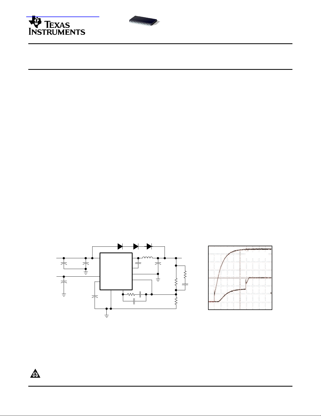
TYPICAL APPLICATION
R = 1.5LW
V = 1.5 V
(core)
V
I/O
= 3.3 V
500 mV/div
t - Time - 5 ms/div
START-UP WAVEFORM
WITH 3 PRECHARGE DIODES
VIN
Voltage
Input 2
查询TPS54073PWPR供应商
2.2 – 4 -V, 14-A SYNCHRONOUS BUCK CONVERTER
WITH DISABLED SINKING DURING START-UP
FEATURES DESCRIPTION
• 8-m Ω MOSFET Switches for High Efficiency at
14.5-A Peak Output Current
• Separate Low-Voltage Power Bus
• Disabled Current Sinking During Start-Up
• Adjustable Output Voltage Down to 0.9 V
• Wide PWM Frequency: Fixed 350 kHz, 550 kHz
or Adjustable 280 kHz to 700 kHz
• Synchronizable to 700 kHz
• Load Protected by Peak Current Limit and
Thermal Shutdown
• Integrated Solution Reduces Board Area and
Total Cost
APPLICATIONS
• Low-Voltage, High-Density Distributed Power
Systems
• Point of Load Regulation for High-
Performance DSPs, FPGAs, ASICs, and
Microprocessors
• Broadband, Networking, and Optical
Communications Infrastructure
• Power PC Series Processors
TPS54073
SLVS547 – FEBRUARY 2005
As a member of the SWIFT™family of dc/dc regulators, the TPS54073 low-input voltage high-output
current synchronous buck PWM converter integrates
all required active components. Included on the
substrate with the listed features are a true, high
performance, voltage error amplifier that enables
maximum performance and flexibility in choosing the
output filter L and C components; an
undervoltage-lockout circuit to prevent start-up until
the input voltage reaches 3 V; an internally or
externally set slow-start circuit to limit in-rush
currents; and a power good output useful for
processor/logic reset, fault signaling, and supply sequencing.
For reliable power up in output precharge applications, the TPS54073 is designed to only source
current during start-up.
The TPS54073 is available in a thermally enhanced
28-pin TSSOP (PWP) PowerPAD™ package, which
eliminates bulky heatsinks. TI provides evaluation
modules and the SWIFT™ designer software tool to
aid in quickly achieving high-performance power
supply designs to meet aggressive equipment development cycles
SWIFT, PowerPAD are trademarks of Texas Instruments.
PRODUCTION DATA information is current as of publication date.
Products conform to specifications per the terms of the Texas
Instruments standard warranty. Production processing does not
necessarily include testing of all parameters.
Please be aware that an important notice concerning availability, standard warranty, and use in critical applications of Texas
Instruments semiconductor products and disclaimers thereto appears at the end of this data sheet.
Copyright © 2005, Texas Instruments Incorporated
www.ti.com
TPS54073
SLVS547 – FEBRUARY 2005
These devices have limited built-in ESD protection. The leads should be shorted together or the device
placed in conductive foam during storage or handling to prevent electrostatic damage to the MOS gates.
ORDERING INFORMATION
T
A
-40 ° C to 85 ° C Adjustible down to 0.9 V Plastic HTSSOP (PWP)
(1) The PWP package is also available taped and reeled. Add an R suffix to the device type (i.e., TPS54073PWPR). See the application
section of the data sheet for PowerPAD drawing and layout information.
ABSOLUTE MAXIMUM RATINGS
over operating free-air temperature range (unless otherwise noted)
V
I
V
O
V
O
I
S
T
J
T
stg
(1) Stresses beyond those listed under “absolute maximum ratings” may cause permanent damage to the device. These are stress ratings
Input voltage range VSENSE –0.3 to 4 V
Output voltage range V
Source current
Sink current COMP 6 mA
Voltage differential AGND to PGND ± 0.3 V
Operating junction temperature range –40 to 125 ° C
Storage temperature range –65 to 150 ° C
Lead temperature 1,6 mm (1/16 inch) from case for 10 seconds 300 ° C
Electrostatic Discharge (ESD) ratings
only, and functional operation of the device at these or any other conditions beyond those indicated under “recommended operating
conditions” is not implied. Exposure to absolute-maximum-rated conditions for extended periods may affect device reliability.
OUTPUT VOLTAGE PACKAGE PART NUMBER
(1)
(1)
TPS54073 UNIT
SS/ENA, SYNC –0.3 to 7
RT –0.3 to 6
PVIN, VIN –0.3 to 4.5
BOOT –0.3 to 10
VBIAS, COMP, PWRGD –0.3 to 7
PH –0.6 to 6
PH Internally limited
COMP, VBIAS 6 mA
PH 25 A
SS/ENA, PWRGD 10
Human body model (HBM) 1 kV
CDM 1000 V
TPS54073PWP
RECOMMENDED OPERATING CONDITIONS
MIN NOM MAX UNIT
V
Input voltage, VIN 3 4 V
I
Power Input voltage, PVIN 2.2 4 V
T
Operating junction temperature –40 125 ° C
J
DISSIPATION RATINGS
PACKAGE
28-Pin PWP with solder 14.87 ° C/W 6.72 W
(1) For more information on the PWP package, see TI technical brief, literature number SLMA002 .
(2) Test board conditions:
a. 3 inch x 3 inch, 4 layers, thickness = 0.062 inch
b. 2-ounce copper traces located on die top of the PCB.
c. 2-ounce copper mixed plane and traces on the bottom of the PCB.
d. 2-ounce copper ground planes on the two internal layers of the PCB.
e. 12 thermal vias (see the Figure 11 in the Application Section of this data sheet.
(3) Maximum power dissipation may be limited by over current protection.
2
(1) (2)
THERMAL IMPEDANCE TA= 25 ° C TA= 70 ° C TA= 85 ° C
JUNCTION-TO-AMBIENT POWER RATING POWER RATING POWER RATING
(3)
3.69 W 2.69 W
www.ti.com
DISSIPATION RATINGS (continued)
PACKAGE
28-Pin PWP without solder
(4)
THERMAL IMPEDANCE TA= 25 ° C TA= 70 ° C TA= 85 ° C
JUNCTION-TO-AMBIENT POWER RATING POWER RATING POWER RATING
27.9 ° C/W 3.58 W 1.97 W 1.43 W
ELECTRICAL CHARACTERISTICS
TJ= -40 ° C to 125 ° C, VIN = 3 V to 4 V, PVIN = 2.2 V to 4 V (unless otherwise noted)
PARAMETER TEST CONDITIONS MIN TYP MAX UNIT
SUPPLY VOLTAGE, VIN
V
Input voltage, VIN 3 4 V
I
Supply voltage range, PVIN Output = 1.8 V 2.2 4 V
fs= 350 kHz, RT open, PH pin open, SYNC = 0 V,
PVIN = 2.5 V
VIN = 3.3 V fs= 550 kHz, RT open, PH pin open, SYNC ≥ 2.5 V, 8.6 13 mA
I
Quiescent current
Q
PVIN = 2.5 V fs= 550 kHz, RT open, PH pin open, SYNC ≥ 2.5 V,
UNDERVOLTAGE LOCKOUT (VIN)
Start threshold voltage, UVLO 2.9 3 V
Stop threshold voltage, UVLO 2.7 2.8 V
Hysteresis voltage, UVLO 100 mV
Rising and falling edge deglitch, UVLO
BIAS VOLTAGE
Output voltage, VBIAS I
Output current, VBIAS
(2)
CUMULATIVE REFERENCE
V
Accuracy 0.882 0.891 0.900 V
ref
REGULATION
Line regulation
Load regulation
(1) (3)
(1) (3)
OSCILLATOR
Internally set—free running frequency kHz
Externally set—free running frequency range RT = 100 k Ω (1% resistor to AGND) 460 500 540 kHz
High-level threshold voltage, SYNC 2.5 V
Low-level threshold voltage, SYNC 0.8 V
Pulse duration, SYNC
(1)
Frequency range, SYNC 300 700 kHz
Ramp valley
Ramp amplitude (peak-to-peak)
Minimum controllable on time
Maximum duty cycle
(1)
(1)
(1)
(1)
(4) Estimated performance
(1) Specified by design
(2) Static resistive loads only
(3) Specified by the circuit used in Figure 12
(1)
PVIN = 2.5 V
SHUTDOWN, SS/ENA = 0 V, PVIN = 2.5 V 1 1.4 mA
fs= 350 kHz, RT open, PH pin open, SYNC = 0 V,
VIN = 3.3 V
VIN = 3.3 V
SHUTDOWN, SS/ENA = 0 V, VIN = 3.3 V < 140 µA
= 0 2.7 2.8 2.9 V
(VBIAS)
IL= 7 A, fs= 350 kHz, TJ= 85 ° C 0.05 %/V
IL= 0 A to 14 A, fs= 350 kHz, TJ= 85 ° C
PVIN = 2.5 V, VIN = 3.3 V
(1)
RT open
RT open
, SYNC ≤ 0.8 V 280 350 420
(1)
, SYNC ≥ 2.5 V 440 550 660
RT = 180 k Ω (1% resistor to AGND)
RT = 68 k Ω (1% resistor to AGND)
TPS54073
SLVS547 – FEBRUARY 2005
6.3 10 mA
3.2 6 mA
4.4 7 mA
2.5 µs
100 µA
0.013 %/A
(1)
(1)
252 280 308
663 700 762
50 ns
0.75 V
1 V
200 ns
90%
3
www.ti.com
TPS54073
SLVS547 – FEBRUARY 2005
ELECTRICAL CHARACTERISTICS (continued)
TJ= -40 ° C to 125 ° C, VIN = 3 V to 4 V, PVIN = 2.2 V to 4 V (unless otherwise noted)
PARAMETER TEST CONDITIONS MIN TYP MAX UNIT
ERROR AMPLIFIER
(4)
(4)
ref
(4)
(4)
PWM COMPARATOR
SLOW-START/ENABLE
POWER GOOD
CURRENT LIMIT
THERMAL SHUTDOWN
OUTPUT POWER MOSFETS
r
DS(on)
Error amplifier open-loop voltage gain 1 k Ω COMP to AGND
Error amplifier unity gain bandwidth Parallel 10 k Ω , 160 pF COMP to AGND
Error amplifier common mode input voltage
range
Powered by internal LDO
Input bias current, VSENSE VSENSE = V
Output voltage slew rate (symmetric), COMP 1 1.4 V/µs
PWM comparator propagation delay time, PWM
comparator input to PH pin (excluding 10-mV overdrive
deadtime)
Enable threshold voltage, SS/ENA 0.82 1.2 1.4 V
Enable hysteresis voltage, SS/ENA
Falling edge deglitch, SS/ENA
(4)
(4)
Internal slow-start time 2.6 3.35 4.1 ms
Charge current, SS/ENA SS/ENA = 0 V 2 5 8 µA
Discharge current, SS/ENA SS/ENA = 0.2 V, VIN = 2.7 V, PVIN = 2.5 V 1.3 2.3 4 mA
Power-good threshold voltage VSENSE falling 93 %V
Power-good hysteresis voltage
Power-good falling edge deglitch
Output saturation voltage, PWRGD I
(4)
(4)
= 2.5 mA 0.18 0.3 V
(sink)
Leakage current, PWRGD VIN = 3.3 V, PVIN = 2.5 V 1 µA
Current limit VIN = 3.3 V, PVIN = 2.5 V
Current limit leading edge blanking time
Current limit total response time
Thermal shutdown trip point
Thermal shutdown hysteresis
(4)
(4)
Power MOSFET switches m Ω
(4)
(4)
VIN = 3 V, PVIN = 2.5 V 8 21
VIN = 3.6 V, PVIN = 2.5 V 8 18
90 110 dB
(4)
3 5 MHz
0 VBIAS V
60 250 nA
70 85 ns
0.03 V
2.5 µs
3 %V
35 µs
, Output shorted 14.5 21 A
100 ns
200 ns
135 165 ° C
10 ° C
ref
ref
(4) Specified by design
4
www.ti.com
1
2
3
4
5
6
7
8
9
10
11
12
13
14
28
27
26
25
24
23
22
21
20
19
18
17
16
15
AGND
VSENSE
COMP
PWRGD
BOOT
PH
PH
PH
PH
PH
PH
PH
PH
PH
RT
SYNC
SS/ENA
VBIAS
VIN
PVIN
PVIN
PVIN
PVIN
PGND
PGND
PGND
PGND
PGND
THERMAL
PAD
TPS54073
SLVS547 – FEBRUARY 2005
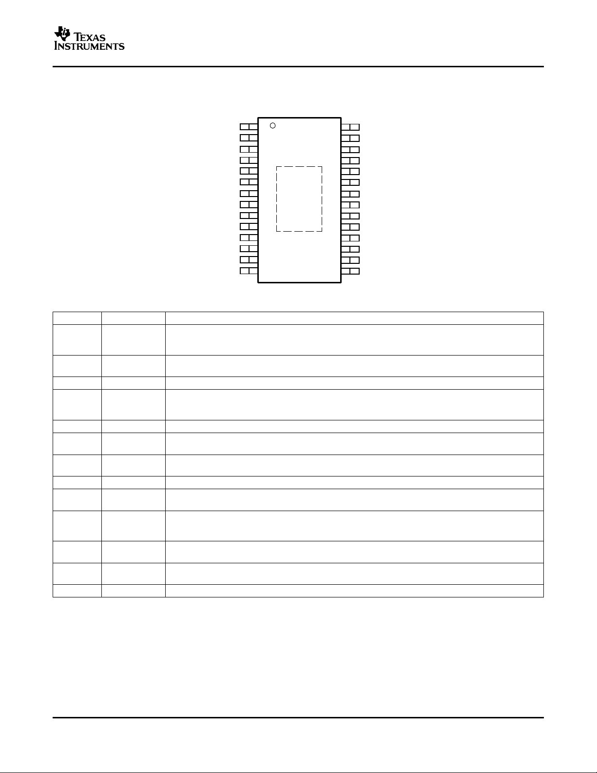
DEVICE INFORMATION
PWP PACKAGE
(TOP VIEW)
TERMINAL FUNCTIONS
PIN NAME PIN NUMBER DESCRIPTION
AGND 1 RT resistor. If using the PowerPAD, connect it to AGND. See the Application Information section for
BOOT 5
COMP 3 Error amplifier output. Connect frequency compensation network from COMP to VSENSE
PGND copper areas to the input and output supply returns, and negative terminals of the input and output
PH 6-14 Phase output. Junction of the internal high-side and low-side power MOSFETs, and output inductor.
PVIN 20, 21, 22, 23
PWRGD 4
RT 28 Frequency setting resistor input. Connect a resistor from RT to AGND to set the switching frequency, fs.
SS/ENA 26
SYNC 27 or pin select between two internally set switching frequencies. When used to synchronize to an external
VBIAS 25
VIN 24
VSENSE 2 Error amplifier inverting input. Connect to output voltage compensation network/output divider.
15, 16, 17, 18,
19
Analog ground. Return for compensation network/output divider, slow-start capacitor, VBIAS capacitor, and
details.
Bootstrap output. 0.022-µF to 0.1-µF low-ESR capacitor connected from BOOT to PH generates floating
drive for the high-side FET driver.
Power ground. High current return for the low-side driver and power MOSFET. Connect PGND with large
capacitors. A single point connection to AGND is recommended.
Input supply for the power MOSFET switches and internal bias regulator. Bypass the PVIN pins to the
PGND pins close to device package with a high-quality, low-ESR 10-µF ceramic capacitor.
Power-good open-drain output. High when VSENSE > 90% V
output is low when SS/ENA is low or the internal shutdown signal is active.
Slow-start/enable input/output. Dual function pin which provides logic input to enable/disable device
operation and capacitor input to externally set the start-up time.
Synchronization input. Dual function pin which provides logic input to synchronize to an external oscillator
signal, a resistor must be connected to the RT pin.
Internal bias regulator output. Supplies regulated voltage to internal circuitry. Bypass VBIAS pin to AGND
pin with a high-quality, low-ESR 0.1-µF to 1.0-µF ceramic capacitor.
Input supply for the internal control circuits. Bypass the VIN pin to the PGND pins close to device package
with a high-quality, low-ESR 1-µF ceramic capacitor.
, otherwise PWRGD is low. Note that
ref
5
www.ti.com
Falling
Edge
Deglitch
Enable
Comparator
1.2 V
VIN
2.95 V
Hysteresis: 0.03 V
2.5 µs
Falling
and
Rising
Edge
Deglitch
2.5 µs
VIN UVLO
Comparator
Hysteresis: 0.11 V
Internal/External
Slow-start
(Internal Slow-start Time = 3.35 ms
Reference
VREF = 0.891 V
−
+
Error
Amplifier
Thermal
Shutdown
150°C
SHUTDOWN
SS_DIS
PWM
Comparator
OSC
Leading
Edge
Blanking
100 ns
R Q
S
Adaptive Dead-Time
and
Control Logic
SHUTDOWN
8 mΩ
VIN
REG
VBIAS
PVIN
BOOT
VIN
PH
C
O
PGND
PWRGD
Falling
Edge
Deglitch
35 µs
VSENSE
SHUTDOWN
0.90 V
ref
Hysteresis: 0.03 Vref
Power-Good
Comparator
AGND
VBIAS
ILIM
Comparator
2.2 − 4.0 V
V
O
RT
COMPVSENSE
SS/ENA
TPS54073
8 mΩ
L
OUT
VIN
3.0 − 4.0 V
SYNC
Start−Up
Driver
Suppression
TPS54073
SLVS547 – FEBRUARY 2005
FUNCTIONAL BLOCK DIAGRAM
6
www.ti.com
TYPICAL CHARACTERISTICS
250
350
450
550
650
750
−40 0 25 85 125
T
J
− Junction Temperature − °C
f − Internally Set Oscillator Frequency − kHz
SYNC ≥ 2.5 V
SYNC ≤ 0.8 V
0
2
4
6
8
10
12
-40 -20 0 20 40 60 80 100
T - Junction Temperature - C
J
o
Drain-Source On-State Resistance - mW
VIN = 3.6 V,
PVIN = 2.5 V,
IO= 9 A
125
0
2
4
6
8
10
12
-40 -20
0 20 40 60 80
100 125
T - Junction Temperature - C
J
o
Drain-Source On-State Resistance - mW
VIN = 3.3 V,
PVIN = 2.5 V,
IO= 9 A
200
300
400
500
600
700
800
−40 0 25 85 125
T
J
− Junction Temperature − °C
f − Externally Set Oscillator Frequency − kHz
RT = 68 kΩ
RT = 100 kΩ
RT = 180 kΩ
0.885
0.887
0.889
0.891
0.893
0.895
−40 0 25 85 125
T
J
− Junction Temperature − °C
− Voltage Reference − V
V
ref
0
0.5
1
1.5
2
2.5
3
3.5
4
4.5
5
0 2 4 6 8 10 12 14 16
- Power Dissipation - W
P
D
I - Output Current - A
O
TA= 25oC
−20
0
20
40
60
80
100
120
140
1 100 1 k 1 M
−200
−180
−160
−140
−120
−100
−80
−60
−40
−20
0
10 10 k 100 k 10 M
f − Frequency − Hz
Gain − dB
Phase − Degrees
Phase
Gain
RL = 10 kΩ,
CL = 160 pF,
TA = 25°C
0.885
0.887
0.889
0.891
0.893
0.895
3 3.1 3.2 3.3 3.4 3.5 3.6
V
I
− Input Voltage − V
− Output Voltage Regulation − V
V
O
PVIN = 2.5 V
2.75
2.90
3.05
3.20
3.35
3.50
3.65
−40 0 25 85 125
T
J
− Junction Temperature − °C
Internal Slow-Start Time − ms
3.80
VIN = 3.3 V,
PVIN = 2.5 V
DRAIN-SOURCE ON-STATE DRAIN-SOURCE ON-STATE INTERNALLY SET OSCILLATOR
RESISTANCE RESISTANCE FREQUENCY
vs vs vs
JUNCTION TEMPERATURE JUNCTION TEMPERATURE JUNCTION TEMPERATURE
Figure 1. Figure 2. Figure 3.
TPS54073
SLVS547 – FEBRUARY 2005
EXTERNALLY SET OSCILLATOR
FREQUENCY VOLTAGE REFERENCE DEVICE POWER DISSIPATION
vs vs vs
JUNCTION TEMPERATURE JUNCTION TEMPERATURE OUTPUT CURRENT
Figure 4. Figure 5. Figure 6.
REFERENCE VOLTAGE INTERNAL SLOWS-START TIME
vs ERROR AMPLIFIER vs
INPUT VOLTAGE OPEN-LOOP RESPONSE JUNCTION TEMPERATURE
Figure 7. Figure 8. Figure 9.
7
www.ti.com
AGND
BOOT
VSENSE
COMP
PWRGD
PH
PH
PH
PH
PH
PH
PH
PH
PH
RT
SYNC
SS/ENA
VBIAS
VIN
PVIN
PVIN
PVIN
PVIN
PGND
PGND
PGND
PGND
PGND
VOUT
PH
PVIN
TOPSIDE GROUND AREA
VIA to Ground Plane
ANALOG GROUND TRACE
EXPOSED
POWERPAD
AREA
COMPENSATION
NETWORK
OUTPUT INDUCTOR
OUTPUT
FILTER
CAPACITOR
BOOT
CAPACITOR
INPUT
BYPASS
CAPACITOR
INPUT
BULK
FILTER
FREQUENCY SET RESISTOR
SLOW START
CAPACITOR
BIAS CAPACITOR
INPUT
BYPASS
CAPACITOR
VIN
OPTIONAL PRE-CHARGE DIODES
CONNECT TO PRE-CHARGE
VOLTAGE SOURCE
TPS54073
SLVS547 – FEBRUARY 2005
PCB LAYOUT
APPLICATION INFORMATION
The PVIN pins are connected together on the printed- ground side of the input and output filter capacitors.
circuit board (PCB) and bypassed with a low ESR The AGND and PGND pins are tied to the PCB
ceramic bypass capacitor. Care should be taken to ground by connecting them to the ground area under
minimize the loop area formed by the bypass capaci- the device as shown in Figure 10 . Use a separate
tor connections, the PVIN pins, and the TPS54073 wide trace for the analog ground signal path. This
ground pins. The minimum recommended bypass analog ground is used for the voltage set point
capacitance is a 10-µF ceramic capacitor with a X5R divider, timing resistor RT, slow-start capacitor, and
or X7R dielectric. The optimum placement is as close bias capacitor grounds. The PH pins are tied together
as possible to the PVIN pins, the AGND, and PGND and routed to the output inductor. Because the PH
pins. See Figure 10 for an example of a board layout. connection is the switching node, an inductor is
If the VIN is connected to a separate source supply, it located close to the PH pins, and the area of the PCB
is bypassed with its own capacitor. There is an area conductor is minimized to prevent excessive capaciof ground on the top layer of the PCB, directly under tive coupling. Connect the boot capacitor between the
the IC, with an exposed area for connection to the phase node and the BOOT pin as shown in Fig-
Figure 10. TPS54073 Layout
PowerPAD. Use vias to connect this ground area to ure 10 . Keep the boot capacitor close to the IC, and
any internal ground planes. Use additional vias at the minimize the conductor trace lengths. Connect the
8

www.ti.com
Connect Pin 1 to Analog Ground Plane
in This Area for Optimum Performance
Minimum Recommended Top
Side Analog Ground Area
0.3478
0.0150
0.06
0.0256
0.1700
0.1340
0.0630
0.0400
Ø0.01804 PL
0.2090
Ø0.0130
8 PL
Minimum Recommended Exposed
Copper Area for PowerPAD. 5mm
Stencils May Require 10 Percent
Larger Area
0.0650
0.0500
0.0500
0.0650
0.0339
0.0339
0.0500
Minimum Recommended Thermal Vias: 8 x 0.013 Diameter Inside
PowerPAD Area 4 x 0.018 Diameter Under Device as Shown.
Additional 0.018 Diameter Vias May Be Used if Top Side Analog Ground
Area Is Extended.
0.3820
TPS54073
SLVS547 – FEBRUARY 2005
output filter capacitor(s) between the VOUT trace and For operation at full rated load current, the analog
PGND. It is important to keep the loop formed by the ground plane must provide an adequate
PH pins, Lout, Cout, and PGND as small as is heat-dissipating area. A 3-inch by 3-inch plane of
practical. Place the compensation components from 1-ounce copper is recommended, though not mandathe VOUT trace to the VSENSE and COMP pins. Do tory, depending on ambient temperature and airflow.
not place these components too close to the PH Most applications have larger areas of internal ground
trace. Due to the size of the IC package and the plane available, and the PowerPAD must be connecdevice pinout, they must be routed close, but main- ted to the largest area available. Additional areas on
tain as much separation as possible while keeping the top or bottom layers also help dissipate heat, and
the layout compact. Connect the bias capacitor from any area available must be used when 6-A or greater
the VBIAS pin to analog ground using the isolated operation is desired. Connection from the exposed
analog ground trace. If a slow-start capacitor or RT area of the PowerPAD to the analog ground plane
resistor is used, or if the SYNC pin is used to select layer must be made using 0.013-inch diameter vias to
350-kHz operating frequency, connect them to this avoid solder wicking through the vias.
trace.
Optional prebias diodes should be connected be- additional vias located under the device package. The
tween the output voltage trace and the prebias size of the vias under the package, but not in the
source. The source is VIN, PVIN, or some other exposed thermal pad area, can be increased to
voltage rail. This is dependent on the user's appli- 0.018. Additional vias beyond the twelve reccation circuit. In some cases, the diodes are not ommended that enhance thermal performance must
required if the prebias voltage is caused by an be included in areas not under the device package.
external load circuit leakage path.
Eight vias must be in the PowerPAD area with four
Figure 11. Recommended Land Pattern for 28-Pin PWP PowerPAD
9

www.ti.com
Connect to Optional
Precharge Voltage
TPS54073
SLVS547 – FEBRUARY 2005
Figure 12. Application Circuit, 3.3 V to 1.5 V
Figure 12 shows the schematic for a typical
TPS54073 application. The TPS54073 provides up to
14-A output current at a nominal output voltage of
1.5 V. Nominal input voltages are 3.3 V for PVIN, and
3.3 V for VIN. For proper thermal performance, the
exposed PowerPAD underneath the device must be
soldered to the printed-circuit board.
DESIGN PROCEDURE
The following design procedure is used to select
component values for the TPS54073. Alternately, the
SWIFT Designer Software is used to generate a
complete design. The SWIFT Designer Software uses
an iterative design procedure and accesses a comprehensive database of components when generating
a design. This section presents a simplified discussion of the design process.
DESIGN PARAMETERS
To begin the design process, a few parameters must
be decided. The designer needs to know:
• Input voltage range
• Output voltage
• Input ripple voltage
• Output ripple voltage
• Output current rating
• Operating frequency
For this design example, use the following as the
input parameters:
DESIGN PARAMETER EXAMPLE VALUE
Input voltage (VIN) 3.3 V
Input voltage range (PVIN) 2.2 to 3.5 V
Output voltage 1.5 V
Input ripple voltage 350 mV
Output ripple voltage 20 mV
Output current rating 14 A
Operating frequency 700 kHz
10

www.ti.com
R4(k)
500 kHz
ƒs(kHz)
100 k
0.8xFIKV
)V(VV
L
SWOUTINDIN(MAX)
OUTIN(MAX)OUT
MIN
´´´
-´
=
I
LMAX
2I
LIMIT(MIN)
I
(MAX)
V
PVIN
I
OUT(MAX)
0.25
C
BULK
ƒ
sw
I
OUT(MAX)
ESR
MAX
I
CIN
I
OUT(MAX)
2
I
L(RMS)
I
2
OUT(MAX)
1
12
V
OUT
V
in(MAX)
V
OUT
V
IN(MAX)
L
OUT
Fsw 0.8
2
TPS54073
SLVS547 – FEBRUARY 2005
SWITCHING FREQUENCY
The switching frequency can be set to either one of
two internally programmed frequencies or set to a
externally programmed frequency. With the RT pin
open, setting the SYNC pin at or above 2.5 V selects
550-kHz operation, while grounding or leaving the
SYNC pin open selects 350-kHz operation. For this
design, the switching frequency is externally programmed using the RT pin. By connecting a resistor
(R4) from RT to AGND, any frequency in the range of
250 kHz to 700 kHz can be set. Use Equation 1 to
for 16 V, and the ripple current capacity is greater
than 3 A at the operating frequency of 700 kHz. Total
ripple current handling is in excess of 10.4 A. It is
important that the maximum ratings for voltage and
current are not exceeded under any circumstance.
OUTPUT FILTER COMPONENTS
Two components need to be selected for the output
filter, L1 and C2. Because the TPS54073 is an
externally compensated device, a wide range of filter
component types and values can be supported.
determine the proper value of RT.
Inductor Selection
(1)
In this example circuit, R4 is calculated to be 71.5 k Ω
To calculate the minimum value of the output inductor, use Equation 4
and the switching frequency is set at 700 kHz.
INPUT CAPACITORS
The TPS54073 requires an input de-coupling capacitor and, depending on the application, a bulk input
capacitor. The minimum value for the de-coupling
capacitor, C9, is 10 µF. A high-quality ceramic type
X5R or X7R is recommended. The voltage rating
should be greater than the maximum input voltage.
Additionally, some bulk capacitance may be needed,
especially if the TPS54073 circuit is not located within
approximately 2 inches from the input voltage source.
The value for this capacitor is not critical but it also
should be rated to handle the maximum input voltage
including ripple voltage, and should filter the output
so that input ripple voltage is acceptable.
This input ripple voltage can be approximated by
Equation 2 :
(2)
Where I
OUT(MAX)
the switching frequency, C
value and ESR
is the maximum load current. ƒ
is the bulk capacitor
is the maximum series resistance
MAX
(BULK)
is
sw
of the bulk capacitor.
The maximum RMS ripple current also needs to be
checked. For worst-case conditions, this can be
approximated by Equation 3 :
(3)
In this case, the input ripple voltage would be 329 mV
and the RMS ripple current would be 7 A. The
maximum voltage across the input capacitors would
be Vin max plus delta Vin/2. The chosen bulk
capacitor, a Sanyo POSCAP 6TPD330M is rated for and the peak inductor current can be found from
6.3 V and 4.4 A of ripple current; two bypass Equation 7
capacitors, TDK C3225X7R1C226KT are each rated
K
is a coefficient that represents the amount of
IND
inductor ripple current relative to the maximum output
current. For designs using low ESR output capacitors
such as ceramics, use K
ESR output capacitors, K
= 0.3. When using higher
IND
IND
= 0.2 yields better
results. If designing for high output currents, the
minimum current limit trip point must also be taken
into consideration when choosing the output inductor.
The minimum current limit trip point for the TPS54073
is 14.5 A. The maximum inductor ripple current can
be calculated using Equation 5 :
For a 14 A maximum output current, the peak-to-peak
inductor ripple current must be less than 1 A. This
corresponds to a K
F
is the nominal switching frequency. Use 0.8
SW
of 0.071 in Equation 4 .
IND
times the nominal switching frequency to account for
internal variations from the set frequency.
The minimum inductor value is calculated to be 1.54
µH. A 2.2-µH inductor which is slightly larger than the
minimum is selected.
For the output filter inductor, it is important that the
RMS current and saturation current ratings not be
exceeded. The RMS inductor current can be found
from Equation 6 :
(4)
(5)
(6)
11

www.ti.com
I
L(PK)
I
=
+
x x
x x x x
OUT(MAX)
V
OUT
V
IN
(MAX)VOUT
1.6 V
IN(MAX)LOUT
F
sw
0.8
I
COUT(RMS)
1
12
V
OUT
V
PVIN(MAX)
V
OUT
V
PVIN(MAX)
L
OUT
F
sw
ESR
MAX
N
C
V
IN(MAX)
L
OUT
Fsw 0.8
V
OUT
V
IN(MAX)
V
OUT
V
PP(MAX)
C
OUT(MIN)
1
L
OUT
K
2 ƒ
CO
2
TPS54073
SLVS547 – FEBRUARY 2005
For this design, the RMS inductor current is 14.001 A,
and the peak inductor current is 14.43 A. The Vishay
IHLP5050CZ-01 style output inductor with a value of
2.2 µH meets these current requirements. Increasing
the inductor value decreases the ripple current and
the corresponding output ripple voltage. The inductor
value can be decreased if more margin in the RMS
current is required. In general, inductor values for use
with the TPS54073 falls in the range of 1 µH to 3.3
µH, depending on the maximum required output
current.
Capacitor Requirements
The important design factors for the output capacitor
are dc voltage rating, ripple current rating, and
equivalent series resistance (ESR). The dc voltage
and ripple current ratings cannot be exceeded. The
ESR is important because along with the inductor
current it determines the amount of output ripple
voltage. The actual value of the output capacitor is
not critical, but some practical limits do exist. Consider the relationship between the desired
closed-loop crossover frequency of the design and
LC corner frequency of the output filter. In general, it
is desirable to keep the closed-loop crossover frequency at less than 1/5 of the switching frequency.
With high switching frequencies such as the 700 kHz
frequency of this design, internal circuit limitations of
the TPS54073 limit the practical maximum crossover
frequency to about 70 kHz. To allow for adequate
phase gain in the compensation network, the LC
corner frequency should be about one decade or so
below the closed-loop crossover frequency. This
limits the minimum capacitor value for the output filter
to:
Where K is the frequency multiplier for the spread
between fLCand fCO. K should be between 5 and 15,
typically 10 for one decade difference. For a desired
crossover of 40-kHz and a 2.2-µH inductor, the
minimum value for the output capacitor is 304 µF
using a minimum K factor of 6.5. Increasing the K
factor would require using a larger capacitance. The
selected output capacitor must be rated for a voltage
greater than the desired output voltage plus one half
the ripple voltage. Any de-rating amount must also be
included. The maximum RMS ripple current in the
output capacitors is given by Equation 9 :
(7)
(9)
The calculated RMS ripple current is 201 mA in the
output capacitors.
The maximum ESR of the output capacitor is determined by the amount of allowable output ripple as
specified in the initial design parameters. The output
ripple voltage is the inductor ripple current times the
ESR of the output filter; therefore, the maximum
specified ESR as listed in the capacitor data is given
by Equation 10 :
(10)
and the maximum ESR required is 29 m Ω . A capacitor that meets these requirements is a Cornell Sanyo
POSCAP 6TPD33M rated at 6.3 V with a maximum
ESR of 0.015 Ω and a ripple current rating of 2 A. An
additional small 0.1-µF ceramic bypass capacitor C13
is a also used.
Other capacitor types work well with the TPS54073,
depending on the needs of the application.
Compensation Components
The external compensation used with the TPS54073
allows for a wide range of output filter configurations.
A large range of capacitor values and types of
dielectric are supported. The design example uses
Type-3 compensation consisting of R1, R3, R5, C6,
C7, and C8. Additionally, R2 along with R1 forms a
voltage divider network that sets the output voltage.
These component reference designators are the
same as those used in the SWIFT Designer
Software. There are a number of different ways to
design a compensation network. This procedure
(8)
outlines a relatively simple procedure that produces
good results with most output filter combinations. Use
the SWIFT Designer Software for designs with unusually high closed-loop crossover frequencies, low
value, low ESR output capacitors such as ceramics
or if you are unsure about the design procedure.
When designing compensation networks for the
TPS54073, a number of factors need to be considered. The gain of the compensated error amplifier
should not be limited by the open-loop amplifier gain
characteristics and should not produce excessive
gain at the switching frequency. Also, the closed-loop
crossover frequency should be set less than one-fifth
12

www.ti.com
2
LCIN(NOM)
Z2Z1CO
INT
V f
fff
f
´
´´
=
4V
IN(NOM)
CO
INT
´
=
f
f
ƒ
LC
1
2 L
OUTCOUT
C6
1
2R1 ƒ
INT
R3
1
C6 ƒ
LC
R2
R1 0.891
V
OUT
0.891
C8
1
2R1 ƒ
LC
ƒ
ESR0
1
2R
ESRCOUT
ƒ
Z1
1
2R3C6
ƒ
Z2
1
2R1C8
R5
1
2C8 ƒ
ESR
ƒ
P1
1
2R5C8
ƒ
P2
1
2R3C7
ƒ
INT
1
2R1C6
C7 =
1
2 R3 x 150000p
of the switching frequency, and the phase margin at
crossover must be greater than 45 degrees. The
general procedure outlined here produces results
consistent with these requirements without going into
great detail about the theory of loop compensation.
First, calculate the output filter LC corner frequency
using Equation 11 :
TPS54073
SLVS547 – FEBRUARY 2005
(18)
For this design, one zero is placed at fLCand the
other at one fourth fLC, so Equation 18 simplifies to:
For the design example, fLC= 5.906 kHz.
The closed-loop crossover frequency should be
chosen to be greater than fLCand less than one-fifth
of the switching frequency. Also, the crossover frequency should not exceed 100 kHz, as the error
amplifier may not provide the desired gain. For this
design, a crossover frequency of 40 kHz was chosen.
This value is chosen for comparatively wide loop
bandwidth while still allowing for adequate phase
boost to insure stability.
Next, calculate the R2 resistor value for the output
voltage of 1.5 V using Equation 12 :
For any TPS54073 design, start with an R1 value of
10 k Ω . R2 is 14.7 k Ω .
Now, the values for the compensation components
that set the poles and zeros of the compensation
network can be calculated. Assuming that R1 >> than
R5 and C6 >> C7, the pole and zero locations are
given by Equation 13 through Equation 20 :
(11)
(19)
It is important to note that these equations are only
valid for the pole and zero locations as specified
The value for C6 is given by Equation 20 :
(20)
The first zero, fZ1is located at one-half the output
filter LC corner frequency; so, R3 can be calculated
from:
(21)
The second zero, fZ2is located at the output filter LC
corner frequency; so, C8 can be calculated from:
(12)
(22)
The first pole, fP1is located to coincide with output
filter ESR zero frequency. This frequency is given by:
(23)
where R
is the equivalent series resistance of the
ESR
output capacitor.
(13)
(14)
In this case, the ESR zero frequency is 48.2 kHz, and
R5 can be calculated from:
Additionally, there is a pole at the origin, which has
unity gain at a frequency:
This pole is used to set the overall gain of the
compensated error amplifier and determines the
closed-loop crossover frequency. Because R1 is
given as 10 k Ω and the nominal crossover frequency
is selected as 40 kHz, the desired f
can be
INT
calculated from Equation 18 :
(15)
(16)
The final pole is placed at a frequency above the
closed-loop crossover frequency high enough to not
(24)
cause the phase to decrease too much at the
crossover frequency while still providing enough attenuation so that there is little or no gain at the
(17)
switching frequency. The f
circuit is set to 150 kHz and the last compensation
pole location for this
P2
component value C7 can be derived:
(25)
Note that capacitors are only available in a limited
range of standard values, so the nearest standard
value has been chosen for each capacitor. The
measured closed-loop response for this design is
shown in Figure 5 .
13

www.ti.com
Connect to Optional
Precharge Voltage
TPS54073
SLVS547 – FEBRUARY 2005
BIAS AND BOOTSTRAP CAPACITORS SNUBBER CIRCUIT
Every TPS54073 design requires a bootstrap capaci- R8 and C14 of the application schematic comprise a
tor, C3, and a bias capacitor, C4. The bootstrap snubber circuit. The snubber is included to reduce
capacitor must be a 0.1 µF. The bootstrap capacitor over-shoot and ringing on the phase node when the
is located between the PH pins and BOOT. The bias internal high side FET turns on. Since the frequency
capacitor is connected between the VBIAS pin and and amplitude of the ringing depends to a large
AGND. The value should be 1.0 µF. Both capacitors degree on parasitic effects, it is best to choose these
should be high-quality ceramic types with X7R or component values based on actual measurements of
X5R grade dielectric for temperature stability. They any design layout. See literature number SLVP100
should be placed as close to the device connection for more detailed information on snubber design
pins as possible.
DESIGN WITH CERAMIC CAPACITORS
POWER GOOD
The TPS54073 is provided with a power-good output capacitors, including the main output filter capacitor,
pin PWRGD. This output is an open-drain output and are used. The compensation network components
is intended to be pulled up to a 3.3-V logic supply. A were calculated using SWIFT Designer Software. See
10-k Ω pullup works well in this application. The Figure 23 through Figure 26 for loop response,
absolute maximum voltage is 6 V, so care must be performance graphs, and switching waveforms for
taken not to connect this pull up to Vin if the this circuit.
maximum input voltage exceeds 6 V.
Figure 13 shows an application where all ceramic
Figure 13. 1.5 V Power Supply With Ceramic Output Capacitors
14

www.ti.com
10 1 M
Gain
-60
60
Phase -
o
-180
180
-50
-40
-30
-20
-10
0
10
20
30
40
50
-150
-120
-90
-60
-30
0
30
60
90
120
150
100 1 k 10 k
100 k
Phase
Gain
f - Frequency - Hz
-0.5
-0.4
-0.3
-0.2
-0.1
0
0.1
0.2
0.3
0.4
0.5
0 2 4 6 8 10 12 14
I - Output Current - A
O
Output Voltage Variation - %
-0.3
-0.25
-0.2
-0.15
-0.1
-0.05
0
0.05
0.1
0.15
0.2
0.25
0.3
2.2 2.4 2.6 2.8 3 3.2 3.4 3.6 3.8 4
IO= 0 A
IO= 7 A
IO= 14 A
Output Voltage Variation - %
VO- Output Voltage - V
t - Time = 500 ns/div
V (RIPPLE) = 10 mV/div (ac coupled)
O
I = 14 A
O
V = 2 V/div
(PH)
t - Time = 500 ns/div
PVIN(RIPPLE) = 100 mV/div
(ac coupled)
I = 14 A
O
V = 2 V/div
(PH)
50
55
60
65
70
75
80
85
90
95
0 2 4 6 8 10 12 14 16
Efficiency - %
I - Output Current - A
O
t - Time = 500 nsec/div
V = 1 V/div
(PH)
I = 500 mA/div (ac coupled)
O
t - Time = 250 s/divm
V (RIPPLE) = 50 mV/div (ac coupled)
O
I = 5 A/div
O
t - Time = 5 ms/div
V (SS/ENA) = 500 mV/div
V = 500 mV/div
O
TPS54073
SLVS547 – FEBRUARY 2005
PERFORMANCE GRAPHS
The performance data for Figure 14 through Figure 22 are for the circuit in Figure 12 . Conditions are PVIN = 2.5
V, VIN = 3.3 V, V
= 1.5 V, fs= 700 kHz, and IO= 7 A, TA= 25 ° C, unless otherwise specified.
O
MEASURED LOOP RESPONSE LOAD REGULATION LINE REGULATION
vs vs vs
FREQUENCY OUTPUT CURRENT INPUT VOLTAGE
Figure 14. Figure 15. Figure 16.
EFFICIENCY
vs
OUTPUT CURRENT INPUT RIPPLE VOLTAGE OUTPUT VOLTAGE RIPPLE
LOAD TRANSIENT RESPONSE WITH PRECHARGE RIPPLE CURRENT
Figure 17. Figure 18. Figure 19.
START-UP WAVEFORM OUTPUT INDUCTOR
Figure 20. Figure 21. Figure 22.
15

www.ti.com
t - Time = 500 ns/div
I = 14 A
O
V(PH) = 2 V/div
V (RIPPLE) = 10 mV/div (ac coupled)
O
t - Time = 250 s/divm
I = 5 A/div
O
V = 100 mV/div (ac coupled)
O
10 1 M
Gain
-50
70
Phase -
O
-150
210
-40
-30
-20
-10
0
10
20
30
40
50
60
-120
-90
-60
-30
0
30
60
90
120
150
180
100 1 k 10 k 100 k
Phase
Gain
f - Frequency - Hz
0
10
20
30
40
50
60
70
80
90
100
110
120
130
0 2 4 6 8 10 12 14 16
I - Output Current - A
O
T - Free-Air Temperature - C
A
o
Safe Operating Area,
T = 125 C
J
o
TPS54073
SLVS547 – FEBRUARY 2005
PERFORMANCE GRAPHS (continued)
The performance data for Figure 23 through Figure 26 are for the circuit in Figure 13 . Conditions are PVIN = VIN
= 3.3 V, V
= 1.5 V, fs= 700 kHz, and IO= 7 A, TA= 25 ° C, unless otherwise specified.
O
MEASURED LOOP RESPONSE
vs
FREQUENCY OUTPUT VOLTAGE RIPPLE LOAD TRANSIENT RESPONSE
Figure 23. Figure 24. Figure 25.
FREE-AIR TEMPERATURE
vs
OUTPUT CURRENT
16
Figure 26.

www.ti.com
V
O(max)
PVIN
(min)
0.9
−
+PVIN
VBIAS
SS/ENA
10 kΩ
10 kΩ
27.4 kΩ
100 kΩ
VIN
1/2 LM293
TPS54073
SLVS547 – FEBRUARY 2005
DETAILED DESCRIPTION
OPERATING WITH SEPARATE PVIN
The TPS54073 is designed to operate with the power
stage (high-side and low-side MOSFETs) and the
PVIN input connected to a separate power source
from VIN. The primary intended application has VIN
connected to a 3.3-V bus and PVIN connected to a
2.5-V bus. The TPS54073 cannot be damaged by
any sequencing of these voltages. However, the
UVLO (see detailed description section) is referenced
to the VIN input. Some conditions may cause undesirable operation.
If PVIN is absent when the VIN input is high, the
slow-start is released, and the PWM circuit goes to
maximum duty factor. When the PVIN input ramps
up, the output of the TPS54073 follows the PVIN
input until enough voltage is present to regulate to the
proper output value.
NOTE:
If the PVIN input is controlled via a fast bus switch, it
results in a hard-start condition and may damage the
load (i.e., whatever is connected to the regulated
output of the TPS54073). If a power-good signal is
not available from the 2.5-V power supply, one can
be generated using a comparator and hold the
SS/ENA pin low until the 2.5-V bus power is good. An
example of this is shown in Figure 27 . This circuit can
also be used to prevent the TPS54073 output from
following the PVIN input while the PVIN power supply
is ramping up.
DISABLED SINKING DURING START-UP
(DSDS)
The DSDS feature enables minimal voltage drooping
of output precharge capacitors at start-up. The
TPS54073 is designed to disable the low-side
MOSFET to prevent sinking current from a precharge
output capacitor during start-up. Once the high-side
MOSFET has been turned on to the maximum duty
cycle limit, the low-side MOSFET is allowed to switch.
Once the maximum duty cycle condition is met, the
converter functions as a sourcing converter until the
SS/ENA is pulled low.
PVIN and VIN can be tied together for 3.3-V bus
operation.
MAXIMUM OUTPUT VOLTAGE
The maximum attainable output voltage is limited by
the minimum voltage at the PVIN pin. Nominal
maximum duty cycle is limited to 90% in the
TPS54073; so, maximum output voltage is:
(26)
Care must be taken while operating when nominal
conditions cause duty cycles near 90%. Load transients can require momentary increases in duty cycle.
If the required duty cycle exceeds 90%, the output
may fall out of regulation.
GROUNDING AND PowerPAD LAYOUT
The TPS54073 has two internal grounds (analog and
power). Inside the TPS54073, the analog ground ties
to all of the noise-sensitive signals, whereas the
power ground ties to the noisier power signals. The
PowerPAD must be tied directly to AGND. Noise
injected between the two grounds can degrade the
performance of the TPS54073, particularly at higher
output currents. However, ground noise on an analog
ground plane can also cause problems with some of
the control and bias signals. For these reasons,
separate analog and power ground planes are recommended. These two planes must tie together
directly at the IC to reduce noise between the two
grounds. The only components that must tie directly
to the power ground plane are the input capacitor, the
output capacitor, the input voltage de-coupling capacitor, and the PGND pins of the TPS54073.
UNDERVOLTAGE LOCKOUT (UVLO)
The TPS54073 incorporates an undervoltage-lockout
circuit to keep the device disabled when the input
voltage (VIN) is insufficient. During power up, internal
circuits are held inactive until VIN exceeds the
nominal UVLO threshold voltage of 2.95 V. Once the
UVLO start threshold is reached, device start-up
begins. The device operates until VIN falls below the
nominal UVLO stop threshold of 2.8 V. Hysteresis in
the UVLO comparator, and a 2.5-µs rising and falling
edge deglitch circuit reduce the likelihood of shutting
the device down due to noise on VIN. UVLO is with
respect to VIN and not PVIN, see the Application
Information section.
Figure 27. Undervoltage Lockout Circuit for PVIN
Using Open-Collector or Open-Drain Comparator
17

www.ti.com
td C
(SS)
1.2 V
5 A
Switching Frequency
100 k
R
500 [kHz]
t
(SS)
C
(SS)
0.7 V
5 A
TPS54073
SLVS547 – FEBRUARY 2005
SLOW-START/ENABLE (SS/ENA)
The slow-start/enable pin provides two functions.
First, the pin acts as an enable (shutdown) control by
keeping the device turned off until the voltage exceeds the start threshold voltage of approximately
1.2 V. When SS/ENA exceeds the enable threshold,
device start-up begins. The reference voltage fed to
the error amplifier is linearly ramped up from 0 V to
0.891 V in 3.35 ms. Similarly, the converter output
voltage reaches regulation in approximately 3.35 ms.
Voltage hysteresis and a 2.5-µs falling edge deglitch
circuit reduce the likelihood of triggering the enable
due to noise.
The second function of the SS/ENA pin provides an
external means of extending the slow-start time with
a low-value capacitor connected between SS/ENA
and AGND.
Adding a capacitor to the SS/ENA pin has two effects
on start-up. First, a delay occurs between release of
the SS/ENA pin and start-up of the output. The delay
is proportional to the slow-start capacitor value and
lasts until the SS/ENA pin reaches the enable
threshold. The start-up delay is approximately:
Second, as the output becomes active, a brief
ramp-up at the internal slow-start rate may be observed before the externally set slow-start rate takes
control and the output rises at a rate proportional to
the slow-start capacitor. The slow-start time set by
the capacitor is approximately:
The actual slow-start time is likely to be less than the
above approximation due to the brief ramp-up at the
internal rate.
VBIAS REGULATOR (VBIAS)
The VBIAS regulator provides internal analog and
digital blocks with a stable supply voltage over
variations in junction temperature and input voltage. A
high-quality, low-ESR, ceramic bypass capacitor is
required on the VBIAS pin. X7R or X5R grade
dielectrics are recommended because their values
are more stable over temperature. The bypass capacitor must be placed close to the VBIAS pin and
returned to AGND.
External loading on VBIAS is allowed, with the
caution that internal circuits require a minimum
VBIAS of 2.7 V, and external loads on VBIAS with ac
or digital-switching noise may degrade performance.
The VBIAS pin may be useful as a reference voltage
for external circuits. VBIAS is derived from the VIN
pin; see the functional block diagram of this data
sheet.
VOLTAGE REFERENCE
The voltage reference system produces a precise V
signal by scaling the output of a temperature stable
bandgap circuit. During manufacture, the bandgap
and scaling circuits are trimmed to produce 0.891 V
at the output of the error amplifier, with the amplifier
connected as a voltage follower. The trim procedure
adds to the high-precision regulation of the
TPS54073, because it cancels offset errors in the
scale and error amplifier circuits.
ref
OSCILLATOR AND PWM RAMP
The oscillator frequency is set to an internally fixed
value of 350 kHz. The oscillator frequency can be
externally adjusted from 280 to 700 kHz by connecting a resistor between the RT pin to ground. The
switching frequency is approximated by the following
equation, where R is the resistance from RT to
AGND:
(27)
(29)
ERROR AMPLIFIER
The high-performance, wide bandwidth, voltage error
amplifier sets the TPS54073 apart from most dc/dc
converters. The user is given the flexibility to use a
wide range of output L and C filter components to suit
(28)
the particular application needs. Type-2 or Type-3
compensation can be employed using external compensation components.
PWM CONTROL
Signals from the error amplifier output, oscillator, and
current limit circuit are processed by the PWM control
logic. Referring to the internal block diagram, the
control logic includes the PWM comparator, OR gate,
PWM latch, and portions of the adaptive dead-time
and control-logic block. During steady-state operation
below the current limit threshold, the PWM
comparator output and oscillator pulse train alternately reset and set the PWM latch. Once the PWM
latch is set, the low-side FET remains on for a
minimum duration set by the oscillator pulse width.
During this period, the PWM ramp discharges rapidly
to its valley voltage. When the ramp begins to charge
back up, the low-side FET turns off and high-side
FET turns on. As the PWM ramp voltage exceeds the
error amplifier output voltage, the PWM comparator
resets the latch, thus turning off the high-side FET
and turning on the low-side FET. The low-side FET
18

www.ti.com
TPS54073
SLVS547 – FEBRUARY 2005
remains on until the next oscillator pulse discharges
the PWM ramp. During transient conditions, the error
amplifier output could be below the PWM ramp valley
voltage or above the PWM peak voltage. If the error
amplifier is high, the PWM latch is never reset, and
the high-side FET remains on until the oscillator pulse
signals the control logic to turn the high-side FET off
and the low-side FET on. The device operates at its
maximum duty cycle until the output voltage rises to
the regulation set-point, setting VSENSE to approximately the same voltage as VREF. If the error
amplifier output is low, the PWM latch is continually
reset and the high-side FET does not turn on. The
low-side FET remains on until the VSENSE voltage
decreases to a range that allows the PWM
comparator to change states. The TPS54073 is
capable of sinking current continuously until the
output reaches the regulation set-point.
If the current limit comparator trips for longer than
100 ns, the PWM latch resets before the PWM ramp
exceeds the error amplifier output. The high-side FET
turns off and low-side FET turns on to decrease the
energy in the output inductor and consequently the
output current. This process is repeated each cycle in
which the current limit comparator is tripped.
DEAD-TIME CONTROL AND MOSFET
DRIVERS
Adaptive dead-time control prevents shoot-through
current from flowing in both N-channel power
MOSFETs during the switching transitions by actively
controlling the turn-on times of the MOSFET drivers.
The high-side driver does not turn on until the voltage
at the gate of the low-side FET is below 2 V. While
the low-side driver does not turn on until the voltage
at the gate of the high-side MOSFET is below 2 V.
The high-side and low-side drivers are designed with
300-mA source and sink capability to quickly drive the
power MOSFETs gates. The low-side driver is supplied from VIN, whereas the high-side driver is
supplied from the BOOT pin. A bootstrap circuit uses
an external BOOT capacitor and an internal 2.5- Ω
bootstrap switch connected between the VIN and
BOOT pins. The integrated bootstrap switch improves
drive efficiency and reduces external component
count.
OVERCURRENT PROTECTION
The cycle-by-cycle current limiting is achieved by
sensing the current flowing through the high-side
MOSFET and comparing this signal to a preset
overcurrent threshold. The high-side MOSFET is
turned off within 200 ns of reaching the current limit
threshold. A 100-ns leading-edge blanking circuit
prevents current limit false tripping. Current limit
detection occurs only when current flows from VIN to
PH when sourcing current to the output filter. Load
protection during current sink operation is provided by
thermal shutdown.
THERMAL SHUTDOWN
The device uses the thermal shutdown to turn off the
power MOSFETs and disable the controller if the
junction temperature exceeds 150 ° C. The device is
released from shutdown automatically when the junction temperature decreases to 10 ° C below the thermal shutdown trip point, and starts up under control
of the slow-start circuit.
Thermal shutdown provides protection when an overload condition is sustained for several milliseconds.
With a persistent fault condition, the device cycles
continuously; starting up by control of the slow-start
circuit, heating up due to the fault condition, and then
shutting down on reaching the thermal shutdown trip
point. This sequence repeats until the fault condition
is removed.
POWER-GOOD (PWRGD)
The power-good circuit monitors for undervoltage
conditions on VSENSE. If the voltage on VSENSE is
10% below the reference voltage, the open-drain
PWRGD output is pulled low. PWRGD is also pulled
low if VIN is less than the UVLO threshold or SS/ENA
is low. When VIN, UVLO threshold, SS/ENA, enable
threshold, and VSENSE > 90% of V
output of the PWRGD pin is high. A hysteresis
voltage equal to 3% of V
and a 35-µs falling-edge
ref
deglitch circuit prevent tripping of the power-good
comparator due to high-frequency noise.
, the open-drain
ref
19


PACKAGE OPTION ADDENDUM
www.ti.com
19-May-2005
PACKAGING INFORMATION
Orderable Device Status
(1)
Package
Type
Package
Drawing
Pins Package
Qty
Eco Plan
TPS54073PWP ACTIVE HTSSOP PWP 28 50 TBD CU NIPDAU Level-1-220C-UNLIM
TPS54073PWPR ACTIVE HTSSOP PWP 28 2000 TBD CU NIPDAU Level-1-220C-UNLIM
(1)
The marketing status values are defined as follows:
ACTIVE: Product device recommended for new designs.
LIFEBUY: TI has announced that the device will be discontinued, and a lifetime-buy period is in effect.
NRND: Not recommended for new designs. Device is in production to support existing customers, but TI does not recommend using this part in
a new design.
PREVIEW: Device has been announced but is not in production. Samples may or may not be available.
OBSOLETE: TI has discontinued the production of the device.
(2)
Eco Plan - The planned eco-friendly classification: Pb-Free (RoHS) or Green (RoHS & no Sb/Br) - please check
http://www.ti.com/productcontent for the latest availability information and additional product content details.
TBD: The Pb-Free/Green conversion plan has not been defined.
Pb-Free (RoHS): TI's terms "Lead-Free" or "Pb-Free" mean semiconductor products that are compatible with the current RoHS requirements
for all 6 substances, including the requirement that lead not exceed 0.1% by weight in homogeneous materials. Where designed to be soldered
at high temperatures, TI Pb-Free products are suitable for use in specified lead-free processes.
Green (RoHS & no Sb/Br): TI defines "Green" to mean Pb-Free (RoHS compatible), and free of Bromine (Br) and Antimony (Sb) based flame
retardants (Br or Sb do not exceed 0.1% by weight in homogeneous material)
(3)
MSL, Peak Temp. -- The Moisture Sensitivity Level rating according to the JEDEC industry standard classifications, and peak solder
temperature.
(2)
Lead/Ball Finish MSL Peak Temp
(3)
Important Information and Disclaimer:The information provided on this page represents TI's knowledge and belief as of the date that it is
provided. TI bases its knowledge and belief on information provided by third parties, and makes no representation or warranty as to the
accuracy of such information. Efforts are underway to better integrate information from third parties. TI has taken and continues to take
reasonable steps to provide representative and accurate information but may not have conducted destructive testing or chemical analysis on
incoming materials and chemicals. TI and TI suppliers consider certain information to be proprietary, and thus CAS numbers and other limited
information may not be available for release.
In no event shall TI's liability arising out of such information exceed the total purchase price of the TI part(s) at issue in this document sold by TI
to Customer on an annual basis.
Addendum-Page 1


IMPORTANT NOTICE
Texas Instruments Incorporated and its subsidiaries (TI) reserve the right to make corrections, modifications,
enhancements, improvements, and other changes to its products and services at any time and to discontinue
any product or service without notice. Customers should obtain the latest relevant information before placing
orders and should verify that such information is current and complete. All products are sold subject to TI’s terms
and conditions of sale supplied at the time of order acknowledgment.
TI warrants performance of its hardware products to the specifications applicable at the time of sale in
accordance with TI’s standard warranty. Testing and other quality control techniques are used to the extent TI
deems necessary to support this warranty . Except where mandated by government requirements, testing of all
parameters of each product is not necessarily performed.
TI assumes no liability for applications assistance or customer product design. Customers are responsible for
their products and applications using TI components. To minimize the risks associated with customer products
and applications, customers should provide adequate design and operating safeguards.
TI does not warrant or represent that any license, either express or implied, is granted under any TI patent right,
copyright, mask work right, or other TI intellectual property right relating to any combination, machine, or process
in which TI products or services are used. Information published by TI regarding third-party products or services
does not constitute a license from TI to use such products or services or a warranty or endorsement thereof.
Use of such information may require a license from a third party under the patents or other intellectual property
of the third party, or a license from TI under the patents or other intellectual property of TI.
Reproduction of information in TI data books or data sheets is permissible only if reproduction is without
alteration and is accompanied by all associated warranties, conditions, limitations, and notices. Reproduction
of this information with alteration is an unfair and deceptive business practice. TI is not responsible or liable for
such altered documentation.
Resale of TI products or services with statements different from or beyond the parameters stated by TI for that
product or service voids all express and any implied warranties for the associated TI product or service and
is an unfair and deceptive business practice. TI is not responsible or liable for any such statements.
Following are URLs where you can obtain information on other Texas Instruments products and application
solutions:
Products Applications
Amplifiers amplifier.ti.com Audio www.ti.com/audio
Data Converters dataconverter.ti.com Automotive www.ti.com/automotive
DSP dsp.ti.com Broadband www.ti.com/broadband
Interface interface.ti.com Digital Control www.ti.com/digitalcontrol
Logic logic.ti.com Military www.ti.com/military
Power Mgmt power.ti.com Optical Networking www.ti.com/opticalnetwork
Microcontrollers microcontroller.ti.com Security www.ti.com/security
Telephony www.ti.com/telephony
Video & Imaging www.ti.com/video
Wireless www.ti.com/wireless
Mailing Address: Texas Instruments
Post Office Box 655303 Dallas, Texas 75265
Copyright 2005, Texas Instruments Incorporated

Copyright © Each Manufacturing Company.
All Datasheets cannot be modified without permission.
This datasheet has been download from :
www.AllDataSheet.com
100% Free DataSheet Search Site.
Free Download.
No Register.
Fast Search System.
www.AllDataSheet.com
 Loading...