

TPS51461
VIN
VIN
SW
SW
VIN
PGND
PGND
PGND
SW
SW
SW
BST
EN
MODE
VOUT
COMP
SLEW
VREF
GND
VID0
VID1
PGOOD
V5DRV
V5FILT
19
20
21
22
23
24
1 2 3 4 5 6
12
11
10
9
8
7
18 17 16 15 14 13
VCCSA
VCCSASNS
UDG-10183
ENABLE
VIN
VID0
VID1
+5V
PGOOD
TPS51461
www.ti.com
SLUSAD9B –DECEMBER 2010– REVISED SEPTEMBER 2011
3.3-V/5-V Input, 6-A, D-CAP+™ Mode Synchronous Step-Down Integrated FETs Converter
With 2-Bit VID
Check for Samples: TPS51461
1
FEATURES
2
• Integrated FETs Converter w/TI Proprietary
D-CAP+™ Mode Architecture
• 6-A Maximum Output Current
• Minimum External Parts Count
• Support all MLCC Output Capacitor and
SP/POSCAP
• Auto Skip Mode
• Selectable 700-kHz and 1-MHz Frequency
• Small 4 × 4, 24-Pin, QFN Package
APPLICATIONS
• Low-Voltage Applications Stepping Down from
5-V or 3.3-V Rail
• Notebook/Desktop Computers
DESCRIPTION
The TPS51461 is a fully integrated synchronous buck
regulator employing D-CAP+™. It is used for up to
5-V step-down where system size is at its premium,
performance and optimized BOM are must-haves.
This device fully supports Intel system agent
applications with integrated 2-bit VID function.
The TPS51461 also features two switching frequency
settings (700 kHz and 1 MHz), skip mode, pre-bias
startup, programmable external capacitor soft-start
time/voltage transition time, output discharge, internal
VBST Switch, 2-V reference (±1%), power good and
enable.
The TPS51461 is available in a 4 mm × 4 mm,
24-pin, QFN package (Green RoHs compliant and Pb
free) and is specified from -40°C to 85°C.
1
Please be aware that an important notice concerning availability, standard warranty, and use in critical applications of Texas
Instruments semiconductor products and disclaimers thereto appears at the end of this data sheet.
2D-CAP+ is a trademark of Texas Instruments.
PRODUCTION DATA information is current as of publication date.
Products conform to specifications per the terms of the Texas
Instruments standard warranty. Production processing does not
necessarily include testing of all parameters.
Copyright © 2010–2011, Texas Instruments Incorporated
TPS51461
SLUSAD9B –DECEMBER 2010– REVISED SEPTEMBER 2011
www.ti.com
These devices have limited built-in ESD protection. The leads should be shorted together or the device placed in conductive foam
during storage or handling to prevent electrostatic damage to the MOS gates.
(1)
MINIMUM
QUANTITY
no Pb/Br)
T
A
-40°C to 85°C
PACKAGE
Plastic QFN
(RGE)
ORDERING INFORMATION
(2)
ORDERING NUMBER PINS OUTPUT SUPPLY ECO PLAN
TPS51461RGER 24 Tape and reel 3000 Green (RoHS and
TPS51461RGET 24 Mini reel 250
(1) For the most current package and ordering information, see the Package Option Addendum at the end of this document, or visit the TI
website at www.ti.com.
(2) Package drawings, standard packing quantities, thermal data, symbolization, and PCB design guidelines are available at
www.ti.com/sc/package.
THERMAL INFORMATION
(1)
θ
θ
θ
ψ
ψ
θ
JA
JCtop
JB
JT
JB
JCbot
THERMAL METRIC
Junction-to-ambient thermal resistance 33.6
Junction-to-case (top) thermal resistance 45.0
Junction-to-board thermal resistance 10.8
Junction-to-top characterization parameter 0.2
Junction-to-board characterization parameter 10.4
Junction-to-case (bottom) thermal resistance 3.8
(1) For more information about traditional and new thermal metrics, see the IC Package Thermal Metrics application report, SPRA953.
TPS51461
RGE (24) PIN
UNITS
°C/W
ABSOLUTE MAXIMUM RATINGS
(1)
over operating free-air temperature range (unless otherwise noted)
VALUE UNIT
MIN MAX
VIN, EN, MODE –0.3 7.0
V5DRV, V5FILT, VBST (with respect to SW) –0.3 7.0
Input voltage range VBST –0.3 12.5 V
VID0, VID1 –0.3 3.6
VOUT –1.0 3.6
SW –2.0 7.0
SW (transient 20 ns and E=5 µJ) –3.0
Output voltage range COMP, SLEW, VREF –0.3 3.6 V
PGND –0.3 0.3
PGOOD –0.3 7.0
Electrostatic Discharge V
Storage temperature T
Junction temperature T
Lead temperature 1,6 mm (1/16 inch) from case for 10 seconds 300 ˚C
(1) Stresses beyond those listed under “absolute maximum ratings” may cause permanent damage to the device. These are stress ratings
only and functional operation of the device at these or any other conditions beyond those indicated under “recommended operating
conditions” is not implied. Exposure to absolute-maximum-rated conditions for extended periods may affect device reliability.
Human Body Model (HBM) 2000
Charged Device Model (CDM) 500
stg
J
–55 150 ˚C
–40 150 ˚C
2 Submit Documentation Feedback Copyright © 2010–2011, Texas Instruments Incorporated
Product Folder Link(s): TPS51461
TPS51461
www.ti.com
SLUSAD9B –DECEMBER 2010– REVISED SEPTEMBER 2011
RECOMMENDED OPERATING CONDITIONS
VALUE
MIN TYP MAX
VIN, EN, MODE –0.1 6.5
V5DRV, V5FILT, VBST(with respect to SW) –0.1 5.5
Input voltage range VBST –0.1 11.75 V
VID0, VID1 –0.1 3.5
VOUT –0.8 2.0
SW –1.8 6.5
Output voltage range V
Ambient temperature range, T
COMP, SLEW, VREF –0.1 3.5
PGOOD –0.1 6.5
PGND –0.1 0.1
A
-40 85 °C
UNIT
Copyright © 2010–2011, Texas Instruments Incorporated Submit Documentation Feedback 3
Product Folder Link(s): TPS51461
TPS51461
SLUSAD9B –DECEMBER 2010– REVISED SEPTEMBER 2011
ELECTRICAL CHARACTERISTICS
over recommended free-air temperature range, V
otherwise noted)
PARAMETER CONDITIONS MIN TYP MAX UNIT
SUPPLY: VOLTAGE, CURRENTS AND 5 V UVLO
I
VINSD
V
5VIN
I
5VIN
I
5VINSD
V
V5UVLO
V
V5UVHYS
V
VREFUVLO
V
VREFUVHYS
V
POR5VFILT
VOLTAGE FEEDBACK LOOP: VREF, VOUT, AND VOLTAGE GM AMPLIFIER
V
OUTTOL
V
VREF
I
VREFSNK
G
M
V
DM
I
COMPSRC
V
OFFSET
R
DSCH
f
–3dbVL
CURRENT SENSE: CURRENT SENSE AMPLIFIER, OVER CURRENT AND ZERO CROSSING
A
CSINT
I
OCL
I
OCL(neg)
V
ZXOFF
DRIVERS: BOOT STRAP SWITCH
R
DSONBST
I
BSTLK
(1) Ensured by design, not production tested.
VIN shutdown current EN = 'LO' 0.02 5 µA
5VIN supply voltage V5DRV and V5FILT voltage range 4.5 5.0 5.5 V
5VIN supply current EN =’HI’, V5DRV + V5FILT supply current 1.1 2 mA
5VIN shutdown current EN = ‘LO’, V5DRV + V5FILT shutdown current 10 50 µA
V5FILT UVLO Ramp up; EN = 'HI' 4.2 4.3 4.5 V
V5FILT UVLO hysteresis Falling hysteresis 440 mV
REF UVLO
REF UVLO hysteresis
(1)
(1)
Rising edge of VREF, EN = 'HI' 1.8 V
Reset OVP latch is reset by V5FILT falling below the reset threshold 1.5 2.3 3.1 V
VOUT accuracy V
VREF I
VREF
VREF sink current VREF within tolerance, V
Transconductance 1 mS
Differential mode input voltage 0 80 mV
COMP pin maximum sourcing current V
Input offset voltage TA= 25°C –5 0 5 mV
Output voltage discharge resistance 42 Ω
–3dB Frequency
Internal current sense gain 43 53 57 mV/A
(1)
Gain from the current of the low-side FET to PWM comparator
when PWM = "OFF"
Positive overcurrent limit (valley) 6 7.5 A
Negative overcurrent limit (valley) –6.5 –5.0 A
Zero crossing comp internal offset 0 mV
Internal BST switch on-resistance I
VBST
Internal BST switch leakage current V
= 5.0 V, V
VIN
= 0.8V, No droop –1.5% 0% 1.5%
VOUT
V5DRV
= V
V5FILT
= 0 µA, TA= 25°C 2.01 V
= 2.05 V 2.5 mA
VREF
= 2 V –80 µA
COMP
= 10 mA, TA= 25°C 5 10 Ω
= 14 V, VSW= 7 V, TA= 25°C 1 µA
VBST
www.ti.com
= 5 V, MODE = OPEN, PGND = GND (unless
100 mV
6 MHz
4 Submit Documentation Feedback Copyright © 2010–2011, Texas Instruments Incorporated
Product Folder Link(s): TPS51461
TPS51461
www.ti.com
ELECTRICAL CHARACTERISTICS (continued)
over recommended free-air temperature range, V
otherwise noted)
PARAMETER CONDITIONS MIN TYP MAX UNIT
PROTECTION: OVP, UVP, PGOOD, and THERMAL SHUTDOWN
V
PGDLL
V
PGHYSHL
V
PGDLH
V
PGHYSHH
V
INMINPG
V
OVP
V
UVP
TH
SD
TH
SD(hys)
TIMERS: ON-TIME, MINIMUM OFF TIME, SS, AND I/O TIMINGS
t
ONESHOTC
t
MIN(off)
t
PGDDLY
t
PGDPDLYH
t
PGDPDLYL
t
OVPDLY
t
UVDLYEN
t
UVPDLY
I
SLEW
LOGIC PINS: I/O VOLTAGE AND CURRENT
V
PGDPD
I
PGDLKG
V
ENH
V
ENL
I
EN
V
VIDH
V
VIDL
V
MODETH
I
MODE
R
PD
(2) Ensured by design, not production tested.
(3) See Table 3 for descriptions of MODE parameters.
PGOOD deassert to lower
(PGOOD → Low)
Measured at the VOUT pin w/r/t V
PGOOD high hysteresis 8%
PGOOD de-assert to higher
(PGOOD → Low)
Measured at the VOUT pin w/r/t V
PGOOD high hysteresis -8%
Minimum VIN voltage for valid Measured at the VIN pin with a 2-mA sink current on PGOOD
PGOOD pin
OVP threshold Measured at the VOUT pin w/r/t V
UVP threshold 66% 68% 70%
Thermal shutdown
Thermal Shutdown hysteresis
PWM one-shot
(2)
(2)
(2)
Minimum OFF time 357 ns
Measured at the VOUT pin w/r/t V
begins soft-stop
Latch off controller, attempt soft-stop. 130 °C
Controller re-starts after temperature has dropped 10 °C
V
V
V
SW = PGND, V
PGOOD startup delay time (excl. Delay starts from VOUT = VID code 00 and excludes SLEW
SLEW ramp up time) ramp up time
PGOOD high propagation delay time 50 mV over drive, rising edge 0.8 1 1.2 ms
PGOOD low propagation delay time 50 mV over drive, falling edge 10 µs
OVP delay time Time from the VOUT pin out of +20% of V
Undervoltage fault enable delay (excl. Time from (VOUT = VID code 00) going high to undervoltage
SLEW ramp up time) fault is ready
UVP delay time Time from the VOUT pin out of –30% of V
Soft-start and voltage transition CSS= 10 nF assuming voltage slew rate of 1 mV/µs 9 10 11 µA
PGOOD pull down voltage PGOOD low impedance, I
PGOOD leakage current PGOOD high impedance, forced to 5.5 V –1 0 1 µA
EN logic high EN, VCCP logic 0.8 V
EN logic low EN,VCCP logic 0.3 V
EN input current 1 µA
VID logic high VID0, VID1 0.8 V
VID logic low VID0, VID1 0.3 V
MODE 1 0.08 0.13 0.18
MODE 3 0.37 0.42 0.47
MODE threshold voltage
(3)
MODE 4 0.55 0.60 0.65 V
MODE 5 0.83 0.88 0.93
MODE 7 1.75 1.80 1.85
MODE current 15 µA
VID pull-down resistance 10 kΩ
VIN
VIN
VIN
= 5.0 V, V
VIN
= 5 V, V
= 5 V, V
= 5 V, V
VOUT
VOUT
VOUT
VOUT
SLUSAD9B –DECEMBER 2010– REVISED SEPTEMBER 2011
V5DRV
= V
= 5 V, MODE = OPEN, PGND = GND (unless
V5FILT
SLEW
SLEW
82% 84% 86%
114% 116% 118%
0.9 1.3 1.5 V
SLEW
, device latches OFF,
SLEW
118% 120% 122%
= 0.8 V, fSW= 667 kHz, fixed VID mode 240 ns
= 0.8 V, fSW= 1 MHz, fixed VID mode 160 ns
= 0.8 V, fSW= 1 MHz, DRVL on,
< V
SLEW
3 ms
to OVP fault 0.2 µs
SLEW
3 ms
to UVP fault 8.5 µs
SLEW
SINK
= 4 mA, V
VIN
= V
= 4.5 V 0.3 V
V5FILT
Copyright © 2010–2011, Texas Instruments Incorporated Submit Documentation Feedback 5
Product Folder Link(s): TPS51461
TPS51461RGE
VIN
VIN
SW
SW
VIN
PGND
PGND
PGND
SW
SW
SW
BST
EN
MODE
VOUT
COMP
SLEW
VREF
GND
VID0
VID1
PGOOD
V5DRV
V5FILT
2
3
4
5
6
7 8
9 10
11
1
12
13
14
15
16
17
18
24 23
22 21
20 19
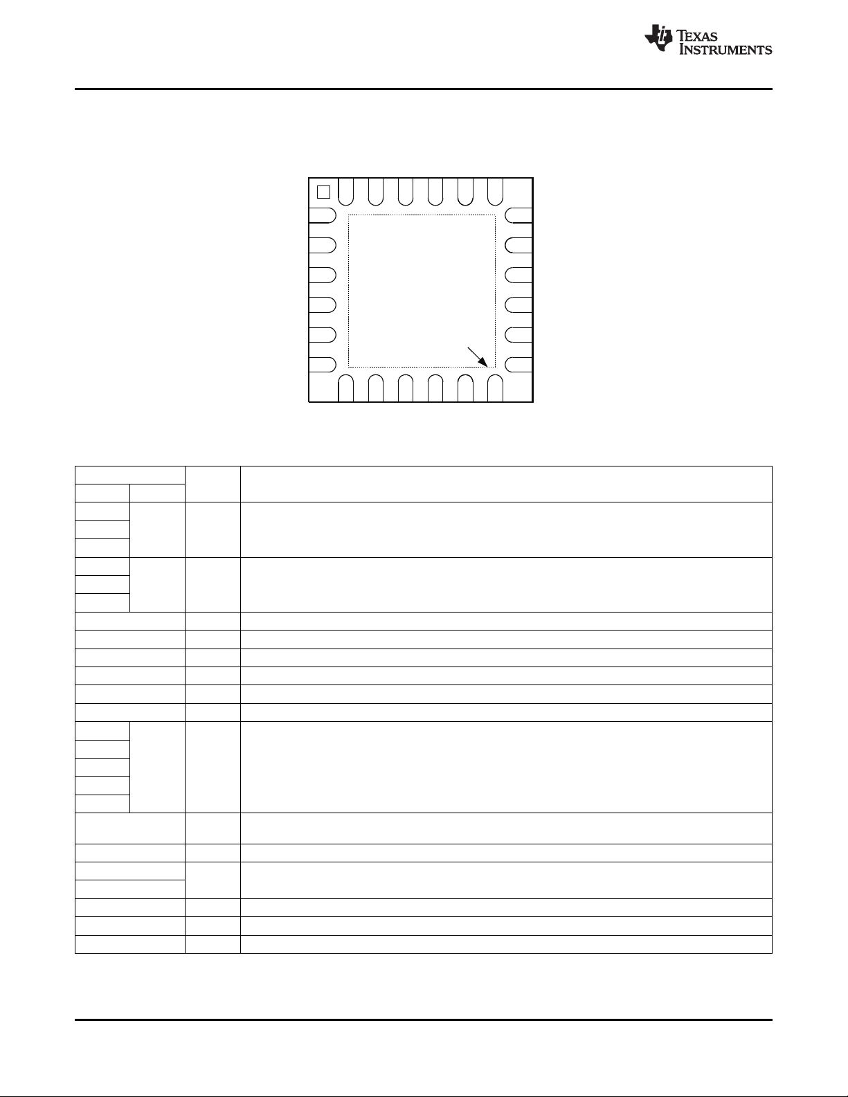
Thermal Pad
TPS51461
SLUSAD9B –DECEMBER 2010– REVISED SEPTEMBER 2011
PIN
NO. NAME
19
20 PGND I Power ground. Source terminal of the rectifying low-side power FET. Positive input for current sensing.
21
22
23 VIN I Power supply input pin. Drain terminal of the switching high-side power FET.
24
1 GND – Signal ground.
2 VREF O 2.0-V reference output. Connect a 0.22-µF ceramic capacitor to GND.
3 COMP O Connect series R/C or R between this pin and VREF for loop compensation.
4 SLEW I/O Program the startup and voltage transition time using an external capacitor via 10-µA current source.
5 VOUT I Output voltage monitor input pin.
6 MODE I Allows selection of switching frequencies and output voltage. (See Table 3)
7
8
9 SW I/O Switching node output. Connect to the external inductor. Also serve as current-sensing negative input.
10
11
12 Power supply for internal high-side gate driver. Connect a 0.1-µF bootstrap capacitor between this pin and
13 EN I Enable of the SMPS.
14 VID0
15 VID1
16 PGOOD O Power good output. Connect pull-up resistor.
17 V5FILT I 5-V power supply for analog circuits.
18 V5DRV I 5-V power supply for the gate driver.
BST I
I/O DESCRIPTION
the SW pin.
I 2-bit VID input.
www.ti.com
RGE PACKAGE
PIN FUNCTIONS
6 Submit Documentation Feedback Copyright © 2010–2011, Texas Instruments Incorporated
Product Folder Link(s): TPS51461
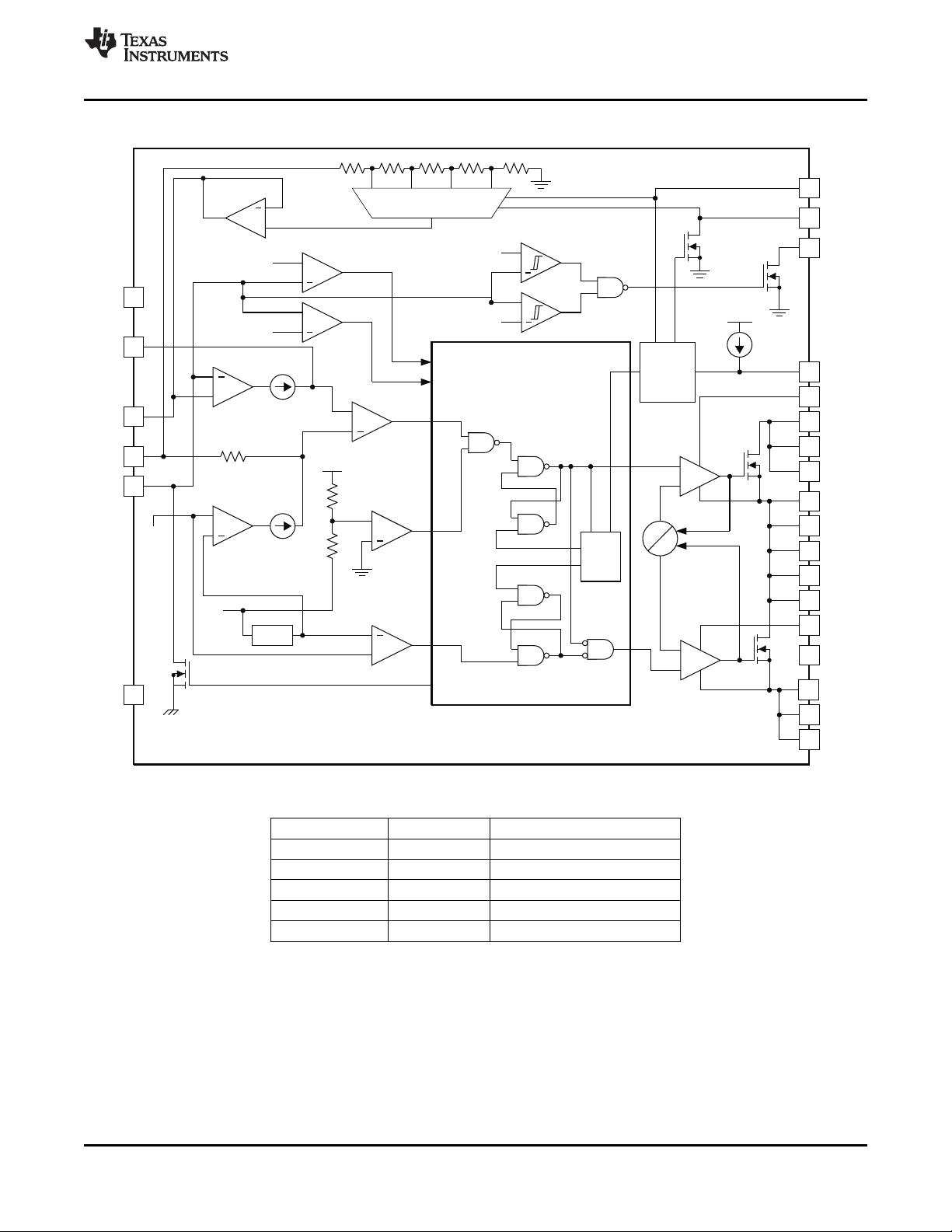
19
7
PGND
SW
TPS51461
OC
ZC
XCON
12 BST
18 V5DRV
PWM
5
EN
16 PGOOD
Control Logic
UDG-10184
+
+
V
REFIN
+20%
+
+
13
VOUT
+
VIN
t
ON
One-
Shot
UV
OV
V
REFIN
–32%
4SLEW
+
8 R
3COMP
R
1GND
2VREF
On-Time
and LL
Selection
15 mA
6 MODE
V
REFIN
+8/16 %
V
REFIN
–8/16 %
+
+
Discharge
UVP
OVP
17 V5FILT
Bandgap
Sense
+
00 01 10 11
+
VS
CS
14 VID0
15 VID1
10 mA
SW
PGND
22
23
24
VIN
VIN
8 SW
9 SW
10 SW
11 SW
20 PGND
21 PGND
VCS
TPS51461
www.ti.com
BLOCK DIAGRAM
SLUSAD9B –DECEMBER 2010– REVISED SEPTEMBER 2011
VID 0 VID 1 VCCSA
0 0 0.9 V
0 1 0.80V
0 1 0.85V
Table 1. Intel SA VID
(1)
MODE = Open
(1)
MODE = 33 kΩ
1 0 0.725 V
1 1 0.675 V
(1) 0.80V for 2011 SV processor and 0.85V for 2011 LV/ULV processor
Copyright © 2010–2011, Texas Instruments Incorporated Submit Documentation Feedback 7
Product Folder Link(s): TPS51461
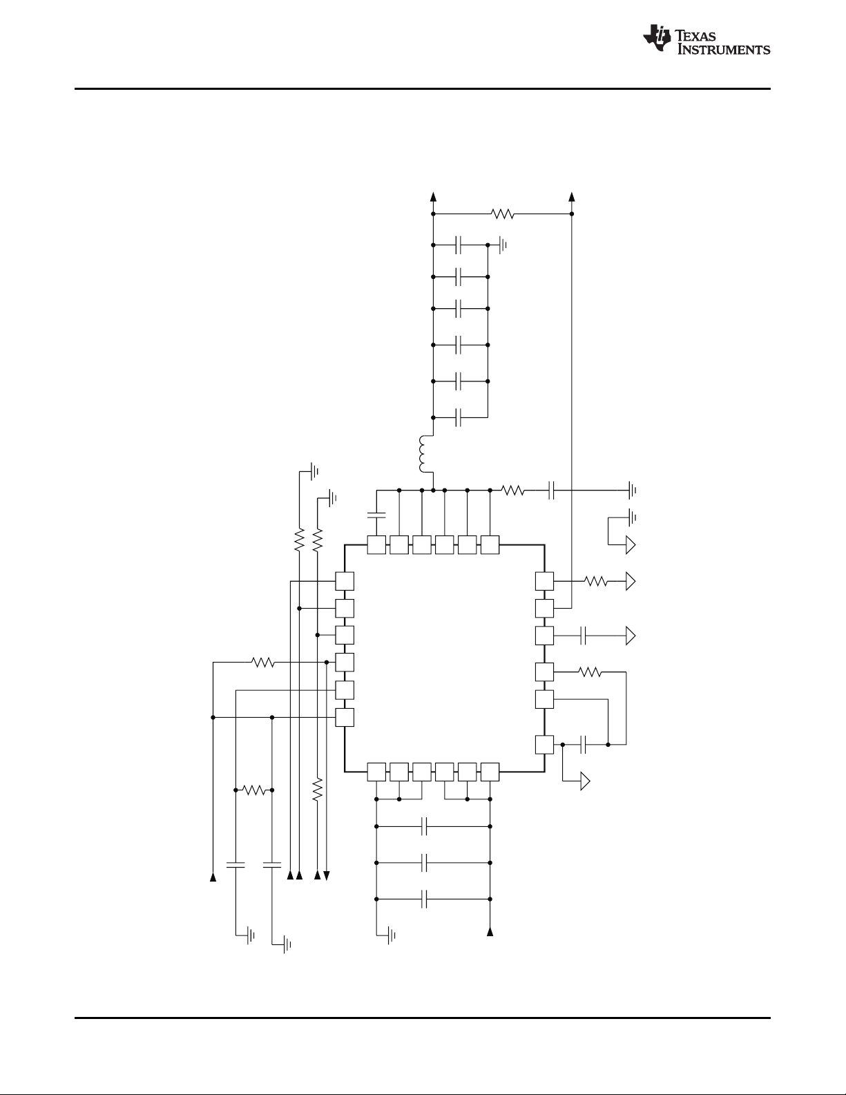
TPS
51461
VIN
VIN
SW
SW
VIN
PGND
PGND
PGND
SWSWSW
BST
EN
MODE
VOUT
COMP
SLEW
VREF
GND
VID0
VID1
PGOOD
V5DRV
V5FILT
19
20
21
22
23
24
1
2
3
4
5
6
12
11
10
9
8
7
18
17
16
15
14
13
0.1
mF
DNP
L
0.42
mH
22 mF
DNP
DNP
VCCSA
VCCSASNS
UDG-10185
0.22
mF
10 k
W
10 nF
ENABLE
VID0VID
1
+5V
0 W
1 mF
2 kW
PGOOD
0.1
mF
10 mF
10 mF
VIN
22 mF
22 mF
22 mF
22 mF
22 mF
2.2
mF
2 kW
100
kW
2 kW
TPS51461
SLUSAD9B –DECEMBER 2010– REVISED SEPTEMBER 2011
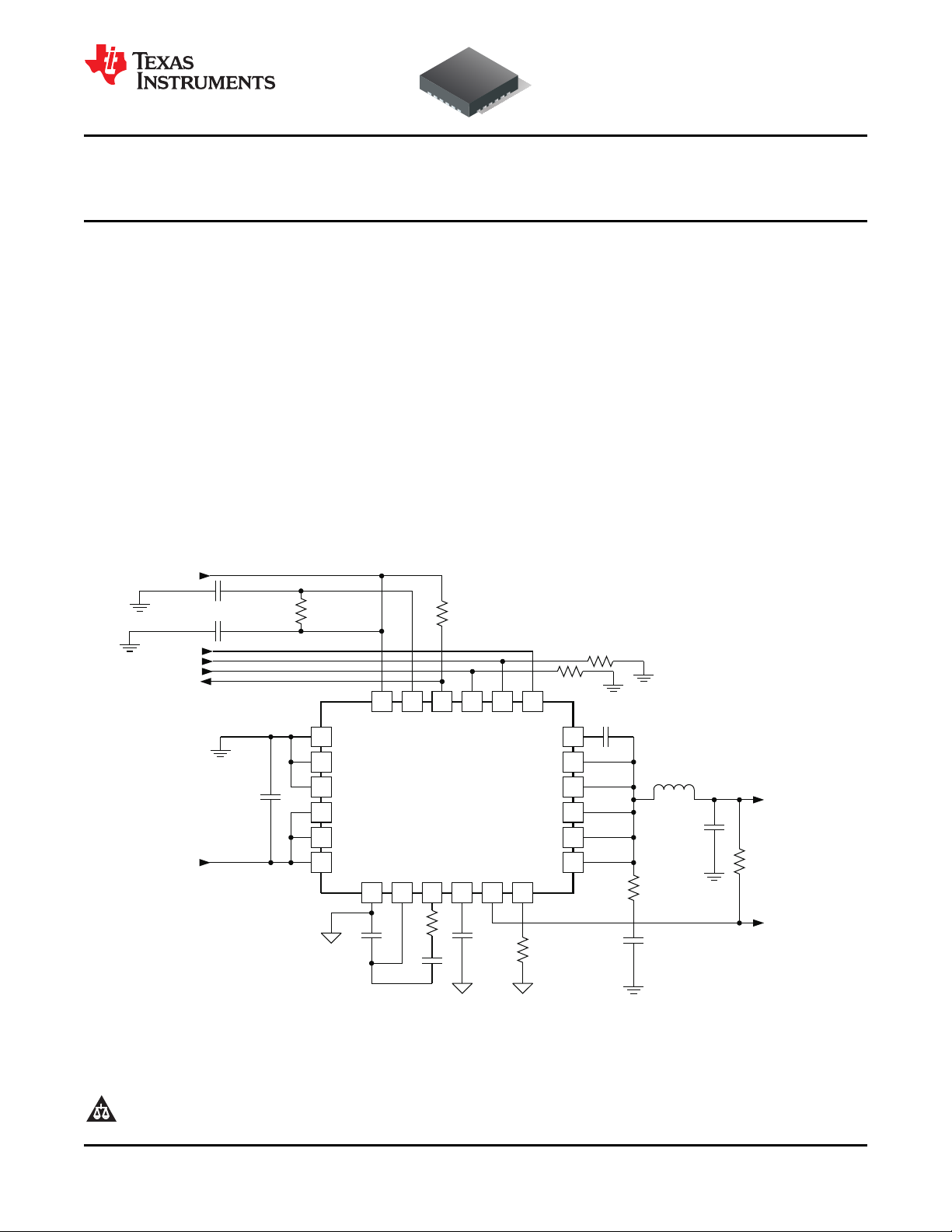
APPLICATION SCHEMATIC WITH TPS51461
www.ti.com
and Recommended Reference Design for Intel SA Application
Figure 1. Application Schematic Using Droop Configuration,
8 Submit Documentation Feedback Copyright © 2010–2011, Texas Instruments Incorporated
Product Folder Link(s): TPS51461

TPS
51461
VIN
VIN
SW
SW
VIN
PGND
PGND
PGND
SWSWSW
BST
EN
MODE
VOUT
COMP
SLEW
VREF
GND
VID0
VID1
PGOOD
V5DRV
V5FILT
19
20
21
22
23
24
1
2
3
4
5
6
12
11
10
9
8
7
18
17
16
15
14
13
0.1
mF
DNP
L
0.42
mH
22 mF
100
W
DNP
DNP
VCCSA
VCCSASNS
UDG-10186
0.22
mF
5 kW
10 nF
ENABLE
VID0VID
1
+5V
0 W
1 mF
2 kW
100
kW
PGOOD
0.1
mF
10 mF
10 mF
VIN
22 mF
22 mF
22 mF
2.2
mF
3.3 nF
2 kW
TPS51461
www.ti.com
SLUSAD9B –DECEMBER 2010– REVISED SEPTEMBER 2011
Copyright © 2010–2011, Texas Instruments Incorporated Submit Documentation Feedback 9
Figure 2. Application Schematic Using Non-Droop Configuration
Product Folder Link(s): TPS51461

TPS51461
SLUSAD9B –DECEMBER 2010– REVISED SEPTEMBER 2011
www.ti.com
Application Circuit List of Materials
Recommended parts for key external components for the circuits in Figure 1 and Figure 2 are listed in Table 2.
Table 2. Key External Component Recommendations
(Figure 1 and Figure 2)
FUNCTION MANUFACTURER PART NUMBER
Output Inductor Nec-Tokin MPCG0740LR42C
Ceramic Output Capacitors
Panasonic ECJ2FB0J226M
Murata GRM21BR60J226ME39L
10 Submit Documentation Feedback Copyright © 2010–2011, Texas Instruments Incorporated
Product Folder Link(s): TPS51461
Time (ms)
Voltage (V)
Current
Feedback
t
ON
t
V
CS
V
COMP
UDG-10187
V
REF
TPS51461
www.ti.com
SLUSAD9B –DECEMBER 2010– REVISED SEPTEMBER 2011
APPLICATION INFORMATION
Functional Overview
The TPS51461 is a D-CAP+™ mode adaptive on-time converter. The output voltage is set using a 2-bit DAC that
outputs a reference voltage in accordance with the code defined in Table 1. VID-on-the-fly transitions are
supported with the slew rate controlled by a single capacitor on the SLEW pin. Integrated high-side and low-side
FET supports output current to a maximum of 6-ADC. The converter automatically runs in discontinuous
conduction mode (DCM) to optimize light-load efficiency. Two switching frequency selections are provided, (700
kHz and 1 MHz) to enable optimization of the power chain for the cost, size and efficiency requirements of the
design.
In adaptive on-time converters, the controller varies the on-time as a function of input and output voltage to
maintain a nearly constant frequency during steady-state conditions. In conventional constant on-time converters,
each cycle begins when the output voltage crosses to a fixed reference level. However, in the TPS51461, the
cycle begins when the current feedback reaches an error voltage level which is the amplified difference between
the reference voltage and the feedback voltage.
PWM Operation
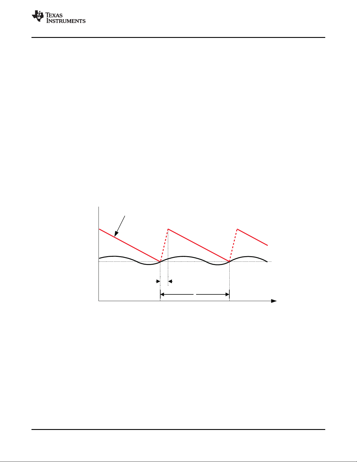
Referring to Figure 3, in steady state, continuous conduction mode, the converter operates in the following way.
Starting with the condition that the top FET is off and the bottom FET is on, the current feedback (VCS) is higher
than the error amplifier output (V
ripple voltage. VCSis not directly accessible by measuring signals on pins of TPS51461. The PWM comparator
senses where the two waveforms cross and triggers the on-time generator.
). VCSfalls until it hits V
COMP
, which contains a component of the output
COMP
Figure 3. D-CAP+™ Mode Basic Waveforms
The current feedback is an amplified and filtered version of the voltage between PGND and SW during low-side
FET on-time. The TPS51461 also provides a single-ended differential voltage (V
system accuracy and reduce the dependence of circuit performance on layout.
Copyright © 2010–2011, Texas Instruments Incorporated Submit Documentation Feedback 11
Product Folder Link(s): TPS51461
) feedback to increase the
OUT

= ´
OUT
ON
IN SW
V
1
t
V f
+
V
SLEW
+
–
R
C
+
PWM
Comparator
R
DS(on)
GMV= 1 mS
Driver
L
OUT
ESR
C
OUT
R
OUT
UDG-10190
R
LOAD
8 kW
+
–
+
GMC= 1 mS
C
C
VREF
TPS51461
SLUSAD9B –DECEMBER 2010– REVISED SEPTEMBER 2011
www.ti.com
PWM Frequency and Adaptive on Time Control
In general, the on-time (at the SW node) can be estimated byEquation 1.
where
• fSWis the frequency selected by the connection of the MODE pin (1)
The on-time pulse is sent to the top FET. The inductor current and the current feedback rises to peak value.
Each ON pulse is latched to prevent double pulsing. Switching frequency settings are shown in Table 3.
Non-Droop Configuration
The TPS51461 can be configured as a non-droop solution. The benefit of a non-droop approach is that load
regulation is flat, therefore, in a system where tight DC tolerance is desired, the non-droop approach is
recommended. For the Intel system agent application, non-droop is recommended as the standard configuration.
The non-droop approach can be implemented by connecting a resistor and a capacitor between the COMP and
the VREF pins. The purpose of the type II compensation is to obtain high DC feedback gain while minimizing the
phase delay at unity gain cross over frequency of the converter.
The value of the resistor (RC) can be calculated using the desired unity gain bandwidth of the converter, and the
value of the capacitor (CC) can be calculated by knowing where the zero location is desired. An application tool
that calculates these values is available from your local TI Field Application Engineer.
Figure 4 shows the basic implementation of the non-droop mode using the TPS51461.
Figure 4. Non-Droop Mode Basic Implementation
Figure 5 shows the load regulation of the system agent rail using non-droop configuration.
Figure 6 shows the transient response of TPS51461 using non-droop configuration where C
applied step load is from 0 A to 2 A.
12 Submit Documentation Feedback Copyright © 2010–2011, Texas Instruments Incorporated
Product Folder Link(s): TPS51461
= 4 × 22 µF. The
OUT

0.73
0.75
0.77
0.79
0.81
0.83
0.85
0.87
0 1 2 3 4 5 6
Output Current (A)
Output Voltage (V)
Mode 3
Mode 4
Mode 7
Mode 8
VIN = 5 V
´
=
´
CSINT
DROOP
DROOP M
A I(L)
V
R G
= = \ =
´ ´
DROOP CSINT CSINT
LOAD _ LINE DROOP
DROOP M LOAD _LINE M
V A A
R R
I(L) R G R G
TPS51461
www.ti.com
SLUSAD9B –DECEMBER 2010– REVISED SEPTEMBER 2011
Figure 5. 0.8-V Load Regulation (VIN= 5 V) Figure 6. Non-Droop Configuration Transient
Non-Droop Configuration Response
Droop Configuration
The terminology for droop is the same as load line or voltage positioning as defined in the Intel CPU V
specification. Based on the actual tolerance requirement of the application, load-line set points can be defined to
maximize either cost savings (by reducing output capacitors) or power reduction benefits.
Accurate droop voltage response is provided by the finite gain of the droop amplifier. The equation for droop
voltage is shown in Equation 2.
CORE
where
• low-side on-resistence is used as the current sensing element
• A
is a constant, which nominally is 53 mV/A.
CSINT
• I(L) is the DC current of the inductor, or the load current
• R
is the value of resistor from the COMP pin to the VREF pin
DROOP
• GMis the transconductance of the droop amplifier with nominal value of 1 mS (2)
Therefore, if a 5-mΩ load line to the system agent rail is desired, the calculated R
Equation 2 can be used to easily derive R
for any load line slope/droop design target.
DROOP
is approximately 10 kΩ.
DROOP
(3)
Copyright © 2010–2011, Texas Instruments Incorporated Submit Documentation Feedback 13
Product Folder Link(s): TPS51461

+
V
SLEW
+
–
R
DROOP
+
PWM
Comparator
R
DS(on)
GMV= 1 mS
Driver
L
OUT
ESR
C
OUT
R
OUT
UDG-10188
R
LOAD
8 kW
+
–
+
GMC= 1 mS
VREF
UDG-10189
Droop
I
LOAD
V
OUT
setpoint at 0 A
Maximum undershoot voltage =(5%–1%) x 1 = 4% x V
OUT
Lead insertion
Lead release
Non-
Droop
Maximum transient voltage
= (5%–1%) x 2 = 8% x V
OUT
V
OUT
setpoint at 6 A
V
OUT
setpoint at 0 A
Maximum overshoot voltage =(5%–1%) x 1 = 4% x V
OUT
TPS51461
SLUSAD9B –DECEMBER 2010– REVISED SEPTEMBER 2011
www.ti.com
Figure 7 shows the basic implementation of the droop mode using the TPS51461.
Figure 7. DROOP Mode Basic Implementation
The droop (voltage positioning) method was originally recommended to reduce the number of external output
capacitors required. The effective transient voltage range is increased because of the active voltage positioning
(see Figure 8).
14 Submit Documentation Feedback Copyright © 2010–2011, Texas Instruments Incorporated
Figure 8. DROOP vs Non-DROOP in Transient Voltage Window
Product Folder Link(s): TPS51461

0.75
0.76
0.77
0.78
0.79
0.80
0.81
0.82
0.83
0.84
0 1 2 3 4 5 6
Output Current (A)
Output Voltage (V)
VIN = 3.3 V
TPS51461
www.ti.com
SLUSAD9B –DECEMBER 2010– REVISED SEPTEMBER 2011
Consider an example of 0.8 V ±5%. If no droop is permitted, the allowable transient overshoot can be at a
maximum of +4%; the allowed transient undershoot can only be at minimum of –4% (given a dc tolerance of
±1%). Therefore, the overshoot and undershoot window is only ±32 mV. If the droop method is applied, this
overshoot and undershoot window could be potentially doubled from ±32 mV to ±64 mV, given the same load
step and release.
In applications where the DC and the AC tolerances are not separated, which means there is not a strict DC
tolerance requirement, the droop method can be used.
Table 3. Mode Parameter Table
COMPENSATION
MODE VREF (V) FREQUENCY VID0 = 0
1 GND X 2.06 1 MHz 0.80
3 22 kΩ X X 2.01 700 kHz 0.80
4 33 kΩ X X 2.01 1 MHz 0.85
5 47 kΩ X 2.06 1 MHz 0.85
7 100 kΩ X X 2.01 700 kHz 0.85
8 Open X X 2.01 1 MHz 0.80
MODE
CONNECTION
Figure 9 shows the load regulation of the 0.8-V rail using an R
TECHNOLOGY
DROOP
NON-
DROOP
DROOP
Figure 10 shows the transient response of the TPS51461 using droop configuration and C
SWITCHING VID1 = 1
(fSW) (V)
value of 10 kΩ.
= 4 × 22 µF. The
OUT
applied step load is from 0 A to 2 A.
Figure 9. 0.8-V Load Regulation (VIN= 3.3 V) Figure 10. Droop Configuration Transient
Copyright © 2010–2011, Texas Instruments Incorporated Submit Documentation Feedback 15
Response
Product Folder Link(s): TPS51461

=
SLEW
SLEW
I
C
SR
´
=
SLEW
SS
SLEW
C 0.9 V
t
I
TPS51461
SLUSAD9B –DECEMBER 2010– REVISED SEPTEMBER 2011
www.ti.com
Light Load Power Saving Features
The TPS51461 has an automatic pulse-skipping mode to provide excellent efficiency over a wide load range.
The converter senses inductor current and prevents negative flow by shutting off the low-side gate driver. This
saves power by eliminating re-circulation of the inductor current. Further, when the bottom FET shuts off, the
converter enters discontinuous mode, and the switching frequency decreases, thus reducing switching losses as
well.
Voltage Slewing
The TPS51461 ramps the SLEW voltage up and down to perform the output voltage transitioning. The timing is
independent of switching frequency, as well as output resistive and capacitive loading. It is set by a capacitor
from SLEW pin to GND, called C
set the startup and voltage transition rate.
where
• I
• SR is the target output voltage slew rate, per Intel specification between 0.5 mV/µs and 10 mV/µs (5)
= 10 µA (nom)
SLEW
For the current reference design, an SR of 1 mV/µs is targeted. The C
slew rate is desired to minimize large inductor current perturbation during startup and voltage transitioning thus
reducing the possibility of acoustic noise.
After the power up, when VID1 is transitioning from 0 to 1, TPS51461 follows the SLEW voltage entering the
forced PWM mode to actively discharge the output voltage from 0.9 V to 0.8 V. The actual output voltage slew
rate is approximately the same as the set slew rate while the bandwidth of the converter supports it and there is
no overcurrent triggered by additional charging current flowing into the output capacitors. After SLEW transition is
completed, PWM mode is maintained for 64 µs (16 clock cycles when the frequency is 1 MHz) to ensure voltage
regulation.
, together with an internal current source of 10 µA. The slew rate is used to
SLEW
is calculated to be 10 nF. The slower
SLEW
(4)
Protection Features
The TPS51461 offers many features to protect the converter power chain as well as the system electronics.
5-V Undervoltage Protection (UVLO)
The TPS51461 continuously monitors the voltage on the V5FILT pin to ensure that the voltage level is high
enough to bias the device properly and to provide sufficient gate drive potential to maintain high efficiency. The
converter starts with approximately 4.3 V and has a nominal of 440 mV of hysteresis. If the 5-V UVLO limit is
reached, the converter transitions the phase node into a 3-state function. And the converter remains in the off
state until the device is reset by cycling 5 V until the 5-V POR is reached (2.3-V nominal). The power input does
not have an UVLO function
Power Good Signals
The TPS51461 has one open-drain power good (PGOOD) pin. During startup, there is a 3 ms power good delay
starting from the output voltage reaching the regulation point (excluding soft-start ramp-up time). And there is
also a 1 ms power good high propagation delay. The PGOOD pin de-asserts as soon as the EN pin is pulled low
or an undervoltage condition on V5FILT is detected. The PGOOD signal is blanked during VID voltage transitions
to prevent false triggering during voltage slewing.
16 Submit Documentation Feedback Copyright © 2010–2011, Texas Instruments Incorporated
Product Folder Link(s): TPS51461

( ) ( )
-
= + ´
P P
OCL dc OCL valley
1
I I I
2
TPS51461
www.ti.com
SLUSAD9B –DECEMBER 2010– REVISED SEPTEMBER 2011
Output Overvoltage Protection (OVP)
In addition to the power good function described above, the TPS51461 has additional OVP and UVP thresholds
and protection circuits.
An OVP condition is detected when the output voltage is approximately 120% × V
. In this case, the
SLEW
converter de-asserts the PGOOD signals and performs the overvoltage protection function. The converter
remains in this state until the device is reset by cycling 5 V until the 5-V POR threshold (2.3 V nominal) is
reached.
Output Undervoltage Protection (UVP)
Output undervoltage protection works in conjunction with the current protection described in the Overcurrent
Protection and Overcurrent Limit sections. If the output voltage drops below 70% of V
, after an 8-µs delay,
SLEW
the device latches OFF. Undervoltage protection can be reset only by EN or a 5-V POR.
Overcurrent Protection
Both positive and negative overcurrent protection are provided in the TPS51461:
• Overcurrent Limit (OCL)
• Negative OCL (level same as positive OCL)
Overcurrent Limit
If the sensed current value is above the OCL setting, the converter delays the next ON pulse until the current
drops below the OCL limit. Current limiting occurs on a pulse-by-pulse basis. The TPS51461 uses a valley
current limiting scheme where the DC OCL trip point is the OCL limit plus half of the inductor ripple current. The
minimum valley OCL is 6 A over process and temperature.
During the overcurrent protection event, the output voltage likely droops until the UVP limit is reached. Then, the
converter de-asserts the PGOOD pin, and then latches OFF after an 8-µs delay. The converter remains in this
state until the device is reset by EN or a 5VFILT POR.
(6)
Negative OCL
The negative OCL circuit acts when the converter is sinking current from the output capacitor(s). The converter
continues to act in a valley mode, the absolute value of the negative OCL set point is typically -6.5 A.
Thermal Protection
Thermal Shutdown
The TPS51461 has an internal temperature sensor. When the temperature reaches a nominal 130°C, the device
shuts down until the temperature cools by approximately 10°C. Then the converter restarts.
Copyright © 2010–2011, Texas Instruments Incorporated Submit Documentation Feedback 17
Product Folder Link(s): TPS51461

VCCP
0.95 V
1.05-V Rail
260 ms
EN
Internal Enable
VID1
(3)
VID0
(3)
SLEW (1 mV/ms)
VOUT
VCCSA_PGOOD
UNCORE_PWRGD
(1)
900 ms 4 ms 2.5 ms
Reset Time
(2)
UDG-10191
TPS51461
SLUSAD9B –DECEMBER 2010– REVISED SEPTEMBER 2011
Startup and VID Transition Timing Diagrams
www.ti.com
For Figure 11:
(1) Includes VCCA, VCCAXG, and VDDQ power rails.
(2) Processor reset: VID transition must be completed by this time.
(3) 1-kΩ pull-down resistor required.
Figure 11. Fixed VID/Fixed Step Startup and VID Toggle Timing Diagram for 2011 Intel Platform
18 Submit Documentation Feedback Copyright © 2010–2011, Texas Instruments Incorporated
Product Folder Link(s): TPS51461

VCCP
0.95 V
1.05-V Rail
260 ms
EN
Internal Enable
VID1
(3)
VID0
(3)
SLEW (1 mV/ms)
VOUT
VCCSA_PGOOD
UNCORE_PWRGD
(1)
900 ms 4 ms 2.5 ms
Reset Time
(2)
UDG-10192
100ms
TPS51461
www.ti.com
SLUSAD9B –DECEMBER 2010– REVISED SEPTEMBER 2011
For Figure 12:
(1) Includes VCCA, VCCAXG, and VDDQ power rails.
(2) Processor reset: VID transition must be completed by this time.
(3) 1-kΩ pull-down resistor required.
Figure 12. Fixed VID/Fixed Step Startup and VID Toggle Timing Diagram for 2012 Intel Platform
Copyright © 2010–2011, Texas Instruments Incorporated Submit Documentation Feedback 19
Product Folder Link(s): TPS51461

40
45
50
55
60
65
70
75
80
85
90
0.01 0.1 1 10
Output Current (A)
Efficiency (%)
Mode 1
Mode 3
Mode 4
Mode 7
Mode 8
TA = 25°C
VIN = 3.3 V
40
45
50
55
60
65
70
75
80
85
90
0.01 0.1 1 10
Output Current (A)
Efficiency (%)
Mode 1
Mode 3
Mode 4
Mode 7
Mode 8
TA = 25°C
VIN = 5 V
0.00
0.25
0.50
0.75
1.00
1.25
0.1 1 10
Output Current (A)
Power Loss (W)
Mode 1
Mode 3
Mode 4
Mode 7
Mode 8
TA = 25°C
VIN = 3.3 V
0.00
0.25
0.50
0.75
1.00
1.25
0.1 1 10
Output Current (A)
Power Loss (W)
Mode 1
Mode 3
Mode 4
Mode 7
Mode 8
TA = 25°C
VIN = 5 V
100
150
200
250
300
350
400
50
0
-30
-20
-10
30
40
50
-40
-50
0
10
20
Frequency (Hz)
Gain
Phase
1000 10 k 100 k 1 M 10 M
Gain (dB)
Phase (°)
25°C
-10°C
85°C
60
110
160
210
260
310
360
10
-40
-30
-20
-10
30
40
50
-40
-50
0
10
20
Frequency (Hz)
Gain
Phase
25°C
-10°C
85°C
1000 10 k 100 k 1 M 10 M
Gain (dB)
Phase (°)
60
TPS51461
SLUSAD9B –DECEMBER 2010– REVISED SEPTEMBER 2011
TYPICAL CHARACTERISTICS
Figure 13. Efficiency vs Output Current Figure 14. Efficiency vs Output Current
www.ti.com
Figure 15. Power Loss Figure 16. Power Loss
20 Submit Documentation Feedback Copyright © 2010–2011, Texas Instruments Incorporated
Figure 17. Bode Plot (Non-Droop Mode) VIN= 5 V, Figure 18. Bode Plot (Droop Mode), VIN= 5 V,
V
= 0.8 V, I
OUT
= 5 A V
LOAD
Product Folder Link(s): TPS51461
OUT
= 0.8 V, I
LOAD
= 5 A

TPS51461
www.ti.com
SLUSAD9B –DECEMBER 2010– REVISED SEPTEMBER 2011
TYPICAL CHARACTERISTICS (continued)
Figure 19. Mode 8 Non-Droop, 0 A Figure 20. Mode 8 Non-Droop, 3 A
Figure 21. Mode 8 Droop, 0 A Figure 22. Mode 8 Droop, 3 A
Figure 23. Mode 4 Non-Droop 0 A Figure 24. Mode 4 Non-Droop 3 A
Copyright © 2010–2011, Texas Instruments Incorporated Submit Documentation Feedback 21
Product Folder Link(s): TPS51461

TPS51461
SLUSAD9B –DECEMBER 2010– REVISED SEPTEMBER 2011
TYPICAL CHARACTERISTICS (continued)
Figure 25. Mode 4 Droop 0 A Figure 26. Mode 4 Droop 3 A
www.ti.com
22 Submit Documentation Feedback Copyright © 2010–2011, Texas Instruments Incorporated
Product Folder Link(s): TPS51461

-
= ´ =
P P
I 6 A 0.25 1.5 A
( )
( )
( )
( )
- -
æ ö
æ ö
- ´
- ´
ç ÷
ç ÷
ç ÷ ç ÷
´
´
´
è ø è ø
= = = = m
10
IN 10
SW IN
P P P P
V
0.8
V V
5 0.8
f V
1 5
V dT
L 0.45 H
I I 1.5 A
m
= = =
m
SLEW
SLEW
DAC
I
10 A
C 10nF
1 mV
SR
s
TPS51461
www.ti.com
SLUSAD9B –DECEMBER 2010– REVISED SEPTEMBER 2011
DESIGN PROCEDURE
The simplified design procedure is done for a non-droop application using the TPS51461 converter.
Step One
Determine the specifications.
The System Agent Rail requirements provide the following key parameters:
1. V00= 0.90 V
2. V10= 0.80 V
3. I
CC(max)
4. I
DYN(max)
5. I
CC(tdc)
Step Two
Determine system parameters.
The input voltage range and operating frequency are of primary interest. For example:
1. VIN= 5 V
2. fSW= 1 MHz
Step Three
Determine inductor value and choose inductor.
Smaller values of inductor have better transient performance but higher ripple and lower efficiency. Higher values
have the opposite characteristics. It is common practice to limit the ripple current to 25% to 50% of the maximum
current. In this case, use 25%:
At fSW= 1 MHz, with a 5-V input and a 0.80-V output:
= 6 A
= 2 A
= 3 A
(7)
For this application, a 0.42-µH, 1.55-mΩ inductor from NEC-TOKIN with part number MPCG0740LR42C is
chosen.
Step Four
Set the output voltage.
The output voltage is determined by the VID settings. The actual voltage set point for each VID setting is listed in
Table 1. No external resistor dividers are needed for this design.
Step Five
Calculate C
VID pin transition and soft-start time is determined by C
SLEW
.
SLEW
The slower slew rate is desired to minimize large inductor current perturbation during startup and voltage
transition, thus reducing the possibility of acoustic noise.
Copyright © 2010–2011, Texas Instruments Incorporated Submit Documentation Feedback 23
Product Folder Link(s): TPS51461
(8)
and 10 µA of internal current source.
(9)

´
´
= = = m
m
SLEW
SS
SLEW
C 0.9 V
10nF 0.9 V
t 900 s
I 10 A
( ) ( )
-
= + ´ = + ´ =
P P
OCL dc OCL valley
1 1
I I I 6 A 1.5 A 6.75 A
2 2
( )
( )
( )
( )
( )
( )
( )
( )
æ ö
´
ç ÷
´ D ´ +
ç ÷
è ø
=
æ ö
æ ö
-
ç ÷
ç ÷
´ D ´ ´ - ´
ç ÷
ç ÷
è ø
è ø
2
VOUT SW
LOAD max MIN off
IN min
OUT min_ under
VOUT
IN min
SW VOUT
LOAD insert MIN off
IN min
V t
L I t
V
C
V V
2 V t t V
V
( )
( )
(
)
( )
´ D
=
´ D ´
2
OUT
LOAD max
OUT min_ over
VOUT
LOAD release
L I
C
2 V V
TPS51461
SLUSAD9B –DECEMBER 2010– REVISED SEPTEMBER 2011
Given the C
, use Equation 10 to calculate the soft start time.
SLEW
www.ti.com
(10)
Step Six
Calculate OCL.
The DC OCL level of TPS51461 design is determined by Equation 11,
(11)
The minimum valley OCL is 6 A over process and temperature, and I
= 1.5 A, the minimum DC OCL is
P-P
calculated to be 6.75A.
Step Seven
Determine the output capacitance.
To determine COUT based on transient and stability requirement, first calculate the the minimum output
capacitance for a given transient.
Equation 13 and Equation 12 can be used to estimate the amount of capacitance needed for a given dynamic
load step/release. Please note that there are other factors that may impact the amount of output capacitance for
a specific design, such as ripple and stability. Equation 13 and Equation 12 are used only to estimate the
transient requirement, the result should be used in conjunction with other factors of the design to determine the
necessary output capacitance for the application.
Equation 12 and Equation 13 calculate the minimum C
72.9 µF assuming the following:
• ±3% voltage allowance for load step and release
• MLCC capacitance derating of 60% due to DC and AC bias effect
In this reference design, 4, 22-µF capacitors are used in order to provide this amount of capacitance.
24 Submit Documentation Feedback Copyright © 2010–2011, Texas Instruments Incorporated
for meeting the transient requirement, which is
OUT
Product Folder Link(s): TPS51461
(12)
(13)

= ´ ´ =
p
C
M
0
OUT S
R
G
1
f 150 kHz
2 C R
´ ´ p´
´ W ´ p´ m
= = » W
0 S OUT
C
M
f R 2 C
150kHz 53m 2 88 F
R 5 k
G 1mS
=
p´ ´
=
0
Z
C C
f
1
f
2 R C 10
TPS51461
www.ti.com
SLUSAD9B –DECEMBER 2010– REVISED SEPTEMBER 2011
Step Eight
Determine the stability based on the output capacitance C
OUT
.
In order to achieve stable operation. The 0-dB frequency, f0should be kept less than 1/5 of the switching
frequency (1 MHz). (See Figure 4)
where
• RS= R
DS(on)
× GMC× R
LOAD
(14)
.
(15)
Using 4, 22-µF capacitors, the compensation resistance, RCcan be calculated to be approximately 5 kΩ.
The purpose of the comparator capacitor (CC) is to reduce the DC component to obtain high DC feedback gain.
However, as it causes phase delay, another zero to cancel this effect at f0is needed. This zero can be
determined by values of CCand the compensation resistor, RC.
(16)
And since RChas previously been derived, the value of CCis calculated to be 2.2 nF. In order to further boost
phase margin, a value of 3.3-nF is chosen for this reference design.
Step Nine
Select decoupling and peripheral components.
For TPS51461 peripheral capacitors use the following minimum values of ceramic capacitance. X5R or better
temperature coefficient is recommended. Tighter tolerances and higher voltage ratings are always appropriate.
• V5DRV decoupling ≥ 2.2 µF, ≥ 10 V
• V5FILT decoupling ≥ 1 µF, ≥10 V
• VREF decoupling 0.22 µF to 1 µF, ≥ 4 V
• Bootstrap capacitors ≥ 0.1 µF, ≥ 10 V
• Pull-up resistors on PGOOD, 100 kΩ
Layout Considerations
Good layout is essential for stable power supply operation. Follow these guidelines for an efficient PCB layout.
• Connect PGND pins (or at least one of the pins) to the thermal PAD underneath the device. Also connect
GND pin to the thermal PAD underneath the device. Use four vias to connect the thermal pad to internal
ground planes.
• Place VIN, V5DRV, V5FILT and 2VREF decoupling capacitors as close to the device as possible.
• Use wide traces for the VIN, VOUT, PGND and SW pins. These nodes carry high current and also serve as
heat sinks.
• Place feedback and compensation components as close to the device as possible.
• Keep analog signals (SLEW, COMP) away from noisy signals (SW, VBST).
Copyright © 2010–2011, Texas Instruments Incorporated Submit Documentation Feedback 25
Product Folder Link(s): TPS51461

TPS51461
SLUSAD9B –DECEMBER 2010– REVISED SEPTEMBER 2011
www.ti.com
Changes from Revision A (DECEMBER 2010) to Revision B Page
• Changed title in Figure 1 to "Droop Configuration". .............................................................................................................. 8
• Changed title in Figure 2 to "Non-Droop Configuration". ...................................................................................................... 9
26 Submit Documentation Feedback Copyright © 2010–2011, Texas Instruments Incorporated
Product Folder Link(s): TPS51461
PACKAGE OPTION ADDENDUM
www.ti.com
11-Apr-2013
PACKAGING INFORMATION
Orderable Device Status
TPS51461RGER ACTIVE VQFN RGE 24 3000 Green (RoHS
TPS51461RGET ACTIVE VQFN RGE 24 250 Green (RoHS
(1)
The marketing status values are defined as follows:
ACTIVE: Product device recommended for new designs.
LIFEBUY: TI has announced that the device will be discontinued, and a lifetime-buy period is in effect.
NRND: Not recommended for new designs. Device is in production to support existing customers, but TI does not recommend using this part in a new design.
PREVIEW: Device has been announced but is not in production. Samples may or may not be available.
OBSOLETE: TI has discontinued the production of the device.
Package Type Package
(1)
Drawing
Pins Package
Qty
Eco Plan
(2)
& no Sb/Br)
& no Sb/Br)
Lead/Ball Finish MSL Peak Temp
(3)
CU NIPDAU Level-2-260C-1 YEAR -40 to 85 TPS
CU NIPDAU Level-2-260C-1 YEAR -40 to 85 TPS
Op Temp (°C) Top-Side Markings
(4)
51461
51461
(2)
Eco Plan - The planned eco-friendly classification: Pb-Free (RoHS), Pb-Free (RoHS Exempt), or Green (RoHS & no Sb/Br) - please check http://www.ti.com/productcontent for the latest availability
information and additional product content details.
TBD: The Pb-Free/Green conversion plan has not been defined.
Pb-Free (RoHS): TI's terms "Lead-Free" or "Pb-Free" mean semiconductor products that are compatible with the current RoHS requirements for all 6 substances, including the requirement that
lead not exceed 0.1% by weight in homogeneous materials. Where designed to be soldered at high temperatures, TI Pb-Free products are suitable for use in specified lead-free processes.
Pb-Free (RoHS Exempt): This component has a RoHS exemption for either 1) lead-based flip-chip solder bumps used between the die and package, or 2) lead-based die adhesive used between
the die and leadframe. The component is otherwise considered Pb-Free (RoHS compatible) as defined above.
Green (RoHS & no Sb/Br): TI defines "Green" to mean Pb-Free (RoHS compatible), and free of Bromine (Br) and Antimony (Sb) based flame retardants (Br or Sb do not exceed 0.1% by weight
in homogeneous material)
(3)
MSL, Peak Temp. -- The Moisture Sensitivity Level rating according to the JEDEC industry standard classifications, and peak solder temperature.
(4)
Multiple Top-Side Markings will be inside parentheses. Only one Top-Side Marking contained in parentheses and separated by a "~" will appear on a device. If a line is indented then it is a
continuation of the previous line and the two combined represent the entire Top-Side Marking for that device.
Important Information and Disclaimer:The information provided on this page represents TI's knowledge and belief as of the date that it is provided. TI bases its knowledge and belief on information
provided by third parties, and makes no representation or warranty as to the accuracy of such information. Efforts are underway to better integrate information from third parties. TI has taken and
continues to take reasonable steps to provide representative and accurate information but may not have conducted destructive testing or chemical analysis on incoming materials and chemicals.
TI and TI suppliers consider certain information to be proprietary, and thus CAS numbers and other limited information may not be available for release.
In no event shall TI's liability arising out of such information exceed the total purchase price of the TI part(s) at issue in this document sold by TI to Customer on an annual basis.
Samples
Addendum-Page 1

PACKAGE MATERIALS INFORMATION
www.ti.com 23-Sep-2014
TAPE AND REEL INFORMATION
*All dimensions are nominal
Device Package
TPS51461RGER VQFN RGE 24 3000 330.0 12.4 4.35 4.35 1.1 8.0 12.0 Q2
TPS51461RGER VQFN RGE 24 3000 330.0 12.4 4.25 4.25 1.15 8.0 12.0 Q2
TPS51461RGET VQFN RGE 24 250 180.0 12.4 4.25 4.25 1.15 8.0 12.0 Q2
TPS51461RGET VQFN RGE 24 250 180.0 12.5 4.35 4.35 1.1 8.0 12.0 Q2
Type
Package
Drawing
Pins SPQ Reel
Diameter
(mm)
Reel
Width
W1 (mm)
A0
(mm)B0(mm)K0(mm)P1(mm)W(mm)
Pin1
Quadrant
Pack Materials-Page 1
PACKAGE MATERIALS INFORMATION
www.ti.com 23-Sep-2014
*All dimensions are nominal
Device Package Type Package Drawing Pins SPQ Length (mm) Width (mm) Height (mm)
TPS51461RGER VQFN RGE 24 3000 338.0 355.0 50.0
TPS51461RGER VQFN RGE 24 3000 367.0 367.0 35.0
TPS51461RGET VQFN RGE 24 250 210.0 185.0 35.0
TPS51461RGET VQFN RGE 24 250 338.0 355.0 50.0
Pack Materials-Page 2


IMPORTANT NOTICE
Texas Instruments Incorporated and its subsidiaries (TI) reserve the right to make corrections, enhancements, improvements and other
changes to its semiconductor products and services per JESD46, latest issue, and to discontinue any product or service per JESD48, latest
issue. Buyers should obtain the latest relevant information before placing orders and should verify that such information is current and
complete. All semiconductor products (also referred to herein as “components”) are sold subject to TI’s terms and conditions of sale
supplied at the time of order acknowledgment.
TI warrants performance of its components to the specifications applicable at the time of sale, in accordance with the warranty in TI’s terms
and conditions of sale of semiconductor products. Testing and other quality control techniques are used to the extent TI deems necessary
to support this warranty. Except where mandated by applicable law, testing of all parameters of each component is not necessarily
performed.
TI assumes no liability for applications assistance or the design of Buyers’ products. Buyers are responsible for their products and
applications using TI components. To minimize the risks associated with Buyers’ products and applications, Buyers should provide
adequate design and operating safeguards.
TI does not warrant or represent that any license, either express or implied, is granted under any patent right, copyright, mask work right, or
other intellectual property right relating to any combination, machine, or process in which TI components or services are used. Information
published by TI regarding third-party products or services does not constitute a license to use such products or services or a warranty or
endorsement thereof. Use of such information may require a license from a third party under the patents or other intellectual property of the
third party, or a license from TI under the patents or other intellectual property of TI.
Reproduction of significant portions of TI information in TI data books or data sheets is permissible only if reproduction is without alteration
and is accompanied by all associated warranties, conditions, limitations, and notices. TI is not responsible or liable for such altered
documentation. Information of third parties may be subject to additional restrictions.
Resale of TI components or services with statements different from or beyond the parameters stated by TI for that component or service
voids all express and any implied warranties for the associated TI component or service and is an unfair and deceptive business practice.
TI is not responsible or liable for any such statements.
Buyer acknowledges and agrees that it is solely responsible for compliance with all legal, regulatory and safety-related requirements
concerning its products, and any use of TI components in its applications, notwithstanding any applications-related information or support
that may be provided by TI. Buyer represents and agrees that it has all the necessary expertise to create and implement safeguards which
anticipate dangerous consequences of failures, monitor failures and their consequences, lessen the likelihood of failures that might cause
harm and take appropriate remedial actions. Buyer will fully indemnify TI and its representatives against any damages arising out of the use
of any TI components in safety-critical applications.
In some cases, TI components may be promoted specifically to facilitate safety-related applications. With such components, TI’s goal is to
help enable customers to design and create their own end-product solutions that meet applicable functional safety standards and
requirements. Nonetheless, such components are subject to these terms.
No TI components are authorized for use in FDA Class III (or similar life-critical medical equipment) unless authorized officers of the parties
have executed a special agreement specifically governing such use.
Only those TI components which TI has specifically designated as military grade or “enhanced plastic” are designed and intended for use in
military/aerospace applications or environments. Buyer acknowledges and agrees that any military or aerospace use of TI components
which have not been so designated is solely at the Buyer's risk, and that Buyer is solely responsible for compliance with all legal and
regulatory requirements in connection with such use.
TI has specifically designated certain components as meeting ISO/TS16949 requirements, mainly for automotive use. In any case of use of
non-designated products, TI will not be responsible for any failure to meet ISO/TS16949.
Products Applications
Audio www.ti.com/audio Automotive and Transportation www.ti.com/automotive
Amplifiers amplifier.ti.com Communications and Telecom www.ti.com/communications
Data Converters dataconverter.ti.com Computers and Peripherals www.ti.com/computers
DLP® Products www.dlp.com Consumer Electronics www.ti.com/consumer-apps
DSP dsp.ti.com Energy and Lighting www.ti.com/energy
Clocks and Timers www.ti.com/clocks Industrial www.ti.com/industrial
Interface interface.ti.com Medical www.ti.com/medical
Logic logic.ti.com Security www.ti.com/security
Power Mgmt power.ti.com Space, Avionics and Defense www.ti.com/space-avionics-defense
Microcontrollers microcontroller.ti.com Video and Imaging www.ti.com/video
RFID www.ti-rfid.com
OMAP Applications Processors www.ti.com/omap TI E2E Community e2e.ti.com
Wireless Connectivity www.ti.com/wirelessconnectivity
Mailing Address: Texas Instruments, Post Office Box 655303, Dallas, Texas 75265
Copyright © 2015, Texas Instruments Incorporated
 Loading...