

TPS51225, TPS51225B, TPS51225C
www.ti.com
SLUSAV0A –JANUARY 2012–REVISED JUNE 2012
Dual Synchronous, Step-Down Controller with 5-V and 3.3-V LDOs
Check for Samples: TPS51225, TPS51225B, TPS51225C
1
FEATURES
2
• Input Voltage Range: 5.5 V to 24 V
• Output Voltages: 5 V and 3.3 V (Adjustable • Netbook, Tablet Computers
Range ±10%)
• Built-in, 100-mA, 5-V and 3.3-V LDOs
• Clock Output for Charge-Pump
• ±1% Reference Accuracy
• Adaptive On-time D-CAP™ Mode Control
Architecture with 300kHz/355kHz Frequency
Setting
• Auto-skip Light Load Operation (TPS51225/C)
• OOA Light Load Operation (TPS51225B)
• Internal 0.8-ms Voltage Servo Soft-Start
• Low-Side R
4500 ppm/°C Temperature Coefficient
• Built-in Output Discharge Function
• Separate Enable Input for Switchers
(TPS51225/B/C)
• Dedicated OC Setting Terminals
• Power Good Indicator
• OVP/UVP/OCP Protection
• Non-latch UVLO/OTP Protection
• 20-Pin, 3 mm × 3 mm, QFN (RUK)
ORDERABLE
DEVICE NUMBER
TPS51225RUKR Tape and Reel 3000
TPS51225RUKT Mini reel 250
TPS51225BRUKR Tape and Reel 3000
TPS51225BRUKT Mini reel 250
TPS51225CRUKR Tape and Reel 3000
TPS51225CRUKT Mini reel 250
(1) For the most current package and ordering information see the Package Option Addendum at the end of this document, or see the TI
website at www.ti.com.
Current Sensing Scheme with
DS(on)
ORDERING INFORMATION
ENABLE OUTPUT
FUNCTION SUPPLY
EN1/ EN2 Auto-skip VREG3
EN1/ EN2 OOA VREG3
EN1/ EN2 Auto-skip VREG3 & VREG5
SKIP MODE ALWAYS ON-LDO PACKAGE QUANTITY
APPLICATIONS
• Notebook Computers
DESCRIPTION
The TPS51225/B/C is a cost-effective, dualsynchronous buck controller targeted for notebook
system-power supply solutions. It provides 5-V and
3.3-V LDOs and requires few external components.
The 260-kHz VCLK output can be used to drive an
external charge pump, generating gate drive voltage
for the load switches without reducing the main
converter efficiency. The TPS51225/B/C supports
high efficiency, fast transient response and provides a
combined power-good signal. Adaptive on-time, DCAP™ control provides convenient and efficient
operation. The device operates with supply input
voltage ranging from 5.5 V to 24 V and supports
output voltages of 5.0 V and 3.3 V. The
TPS51225/B/C is available in a 20-pin, 3 mm × 3
mm, QFN package and is specified from –40°C to
85°C.
(1)
PLASTIC Quad
Flat Pack
(20 pin QFN)
1
Please be aware that an important notice concerning availability, standard warranty, and use in critical applications of
Texas Instruments semiconductor products and disclaimers thereto appears at the end of this data sheet.
2D-CAP, Out-of-Audio are trademarks of Texas Instruments.
PRODUCTION DATA information is current as of publication date.
Products conform to specifications per the terms of the Texas
Instruments standard warranty. Production processing does not
necessarily include testing of all parameters.
Copyright © 2012, Texas Instruments Incorporated
VIN
VBST1
TPS51225 C
DRVH1
SW1
DRVL1
VO1
VFB1
CS1
EN1EN 5 V
VCLK
VREG5
V
IN
5.5 V to 24 V
V
OUT
5 V
V
OUT
15 V
VBST2
DRVH2
SW2
DRVL2
VFB2
CS2
EN2
PGOOD
VREG3
EN 3.3 V
V
OUT
3.3 V
PGOOD
3.3-V Always ON
UDG-12001
1 mF
1 mF
5 V
Always ON
VIN
VBST1
TPS51225
TPS51225 B
DRVH1
SW1
DRVL1
VO1
VFB1
CS1
EN1EN-5V
VCLK
VREG5
V
IN
5.5 V to 24 V
V
OUT
5 V
V
OUT
15 V
VBST2
DRVH2
SW2
DRVL2
VFB2
CS2
EN2
PGOOD
VREG3
EN 3.3 V
V
OUT
3.3 V
PGOOD
3.3-V Always ON
UDG-11182
1 mF
5 V
1 mF
TPS51225, TPS51225B, TPS51225C
SLUSAV0A –JANUARY 2012–REVISED JUNE 2012
These devices have limited built-in ESD protection. The leads should be shorted together or the device placed in conductive foam
during storage or handling to prevent electrostatic damage to the MOS gates.
TYPICAL APPLICATION DIAGRAM (TPS51225/TPS51225B)
www.ti.com
TYPICAL APPLICATION DIAGRAM (TPS51225C)
2 Submit Documentation Feedback Copyright © 2012, Texas Instruments Incorporated
Product Folder Link(s) :TPS51225 TPS51225B TPS51225C
TPS51225, TPS51225B, TPS51225C
www.ti.com
ABSOLUTE MAXIMUM RATINGS
(1)
over operating free-air temperature range (unless otherwise noted)
VBST1, VBST2 –0.3 32
VBST1, VBST2
SW1, SW2 –6.0 26
Input voltage
(2)
VIN –0.3 26 V
EN1, EN2 –0.3 6
VFB1, VFB2 –0.3 3.6
VO1 –0.3 6
DRVH1, DRVH2 –6.0 32
DRVH1, DRVH2
DRVH1, DRVH2
Output voltage
(2)
DRVL1, DRVL2 –0.3 6 V
DRVL1, DRVL2 (pulse width < 20 ns) –2.5 6
PGOOD, VCLK, VREG5 –0.3 6
VREG3, CS1, CS2 –0.3 3.6
Electrostatic
discharge
Junction temperature, T
Storage temperature, T
HBM QSS 009-105 (JESD22-A114A) 2
CDM QSS 009-147 (JESD22-C101B.01) 1
J
ST
(1) Stresses beyond those listed under "absolute maximum ratings" may cause permanent damage to the device. These are stress ratings
only and functional operation of the device at these or any other conditions beyond those indicated under "recommended operating
conditions" is not implied. Exposure to absolute-maximum-rated conditions for extended periods may affect device reliability.
(2) All voltage values are with respect to the network ground terminal unless otherwise noted
(3) Voltage values are with respect to SW terminals.
(3)
(3)
(3)
(pulse width < 20 ns) –2.5 6
SLUSAV0A –JANUARY 2012–REVISED JUNE 2012
VALUE
MIN MAX
UNIT
–0.3 6
–0.3 6
kV
150 °C
–55 150 °C
THERMAL INFORMATION
TPS51225
(1)
θ
θ
θ
ψ
ψ
θ
JA
JCtop
JB
JT
JB
JCbot
THERMAL METRIC
Junction-to-ambient thermal resistance 94.1
Junction-to-case (top) thermal resistance 58.1
Junction-to-board thermal resistance 64.3
Junction-to-top characterization parameter 31.8
Junction-to-board characterization parameter 58.0
Junction-to-case (bottom) thermal resistance 5.9
(1) For more information about traditional and new thermal metrics, see the IC Package Thermal Metrics application report, SPRA953.
TPS51225B
TPS51225C
20-PIN RUK
UNITS
°C/W
Copyright © 2012, Texas Instruments Incorporated Submit Documentation Feedback 3
Product Folder Link(s) :TPS51225 TPS51225B TPS51225C
TPS51225, TPS51225B, TPS51225C
SLUSAV0A –JANUARY 2012–REVISED JUNE 2012
RECOMMENDED OPERATING CONDITIONS
over operating free-air temperature range (unless otherwise noted)
MIN TYP MAX UNIT
Supply voltage VIN 5.5 24
VBST1, VBST2 –0.1 30
VBST1, VBST2
SW1, SW2 –5.5 24 V
Input voltage
(1)
EN1, EN2 –0.1 5.5
VFB1, VFB2 –0.1 3.5
VO1 –0.1 5.5
DRVH1, DRVH2 –5.5 30
DRVH1, DRVH2
Output voltage
(1)
DRVL1, DRVL2 –0.1 5.5 V
PGOOD, VCLK, VREG5 –0.1 5.5
VREG3, CS1, CS2 –0.1 3.5
Operating free-air temperature, T
(1) All voltage values are with respect to the network ground terminal unless otherwise noted.
(2) Voltage values are with respect to the SW terminal.
(2)
(2)
A
–0.1 5.5
–0.1 5.5
–40 85 °C
www.ti.com
4 Submit Documentation Feedback Copyright © 2012, Texas Instruments Incorporated
Product Folder Link(s) :TPS51225 TPS51225B TPS51225C
www.ti.com
ELECTRICAL CHARACTERISTICS
over operating free-air temperature range, V
noted)
PARAMETER TEST CONDITION MIN TYP MAX UNIT
SUPPLY CURRENT
I
VIN1
I
VIN2
I
VO1
I
VIN(STBY)
I
VIN(STBY)
INTERNAL REFERENCE
V
FBx
VREG5 OUTPUT
V
VREG5
I
VREG5
R
V5SW
VREG3 OUTPUT
V
VREG3
I
VREG3
DUTY CYCLE and FREQUENCY CONTROL
f
sw1
f
SW2
T
OFF(MIN)
MOSFET DRIVERS
R
DRVH
R
DRVL
t
D
INTERNAL BOOT STRAP SWITCH
R
VBST (ON)
I
VBSTLK
CLOCK OUTPUT
R
VCLK (PU)
R
VCLK (PD)
f
CLK
(1) Ensured by design. Not production tested.
VIN supply current-1 TA= 25°C, No load, V
VIN supply current-2 TA= 25°C, No load 30 μA
VO1 supply current TA= 25°C, No load, V
VIN stand-by current 95 μA
VIN stand-by current 180 μA
VFB regulation voltage
VREG5 output voltage V
VREG5 current limit V
5-V switch resistance TA= 25°C, V
VREG3 output voltage V
VREG3 current limit V
CH1 frequency
CH2 frequency
(1)
(1)
Minimum off-time TA= 25°C 200 300 500 ns
DRVH resistance Ω
DRVL resistance Ω
Dead time ns
Boost switch on-resistance TA= 25°C, I
VBST leakage current TA= 25°C 1 µA
VCLK on-resistance (pull-up) TA= 25°C 10
VCLK on-resistance (pull-down) TA= 25°C 10
Clock frequency TA= 25°C 260 kHz
TPS51225, TPS51225B, TPS51225C
SLUSAV0A –JANUARY 2012–REVISED JUNE 2012
= 12 V, V
VIN
TA= 25°C, No load, V
V
= V
EN1
EN2
TA= 25°C, No load, V
(TPS51225C)
TA= 25°C 1.99 2.00 2.01 V
TA= 25°C, No load, V
> 7 V , V
VIN
V
> 5.5 V , V
VIN
= 0 V, V
VO1
TA= 25°C, No load, V
V
> 7 V , V
VIN
5.5 V < V
0°C ≤ TA≤ 85°C, V
= 0 V, V
VO1
TA= 25°C, V
TA= 25°C, V
Source, (V
Sink, (V
DRVH
Source, (V
Sink, V
DRVL
DRVH-off to DRVL-on 12
DRVL-off to DRVH-on 20
= 0 V
= 5 V, V
VO1
VO1
VFB1
VO1
VO1
= V
VFB1
VFB2
= 2 V, V
EN1
= V
= 3.3 V (unless otherwise
EN2
=0 V 860 μA
= V
=2.05 V 900 μA
VFB2
= 0 V,
TPS51225
TPS51225B
=0 V, V
EN1=VEN2
=0V
1.98 2.00 2.02 V
= 0 V 4.9 5.0 5.1
VO1
= 0 V, I
VO1
= 0 V, I
VO1
= 4.5 V, V
VREG5
= 5 V, I
VO1
= 0 V, I
VO1
, V
= 0 V, I
VIN
VO1
VIN
= 3.0 V, V
VREG3
= 20 V 240 300 360 kHz
VIN
= 20 V 280 355 430 kHz
VIN
– V
VBST
DRVH
– VSW) = 0.25 V, (V
– V
VREG5
= 0.25 V, V
= 10 mA 13 Ω
VBST
< 100 mA 4.85 5.00 5.10 V
VREG5
< 35 mA 4.85 5.00 5.10
VREG5
= 7 V 100 150 mA
VIN
= 50 mA 1.8 Ω
VREG5
= 0 V 3.267 3.300 3.333
VO1
< 100 mA 3.217 3.300 3.383
VREG3
< 35 mA 3.234 3.300 3.366
VREG3
> 5.5 V, V
) = 0.25 V, (V
) = 0.25 V, V
DRVL
VREG5
= 0 V, I
VO1
= 7 V 100 150 mA
VIN
VBST
– VSW) = 5 V 1.9
VBST
VREG5
< 35 mA 3.267 3.300 3.333
VREG3
– VSW) = 5 V 3.0
= 5 V 3.0
= 5 V 0.9
Ω
Copyright © 2012, Texas Instruments Incorporated Submit Documentation Feedback 5
Product Folder Link(s) :TPS51225 TPS51225B TPS51225C

TPS51225, TPS51225B, TPS51225C
SLUSAV0A –JANUARY 2012–REVISED JUNE 2012
ELECTRICAL CHARACTERISTICS
over operating free-air temperature range, V
noted)
PARAMETER TEST CONDITION MIN TYP MAX UNIT
OUTPUT DISCHARGE
R
DIS1
R
DIS2
R
DIS2
SOFT START OPERATION
t
SS
t
SSRAMP
POWER GOOD
V
PGTH
I
PGMAX
I
PGLK
t
PGDEL
CURRENT SENSING
I
CS
TC
CS
V
CS
V
ZC
LOGIC THRESHOLD
V
ENX(ON)
V
ENX(OFF)
I
EN
OUTPUT OVERVOLTAGE PROTECTION
V
OVP
t
OVPDLY
OUTPUT UNDERVOLTAGE PROTECTION
V
UVP
t
UVPDLY
t
UVPENDLY
UVLO
V
UVL0VIN
V
UVLO5
V
UVLO3
OVER TEMPERATURE PROTECTION
T
OTP
CH1 discharge resistance 35 Ω
CH2 discharge resistance 75 Ω
CH2 discharge resistance TA= 25°C, V
Soft-start time From ENx="Hi" and V
Soft-start time (ramp-up) V
PG threshold
PG sink current V
PG leak current V
PG delay From PG lower threshold (95%=typ) to PG flag high 0.7 ms
CS source current TA= 25°C, VCS= 0.4 V 9 10 11 μA
CS current temperature coefficient
CS Current limit setting range 0.2 2 V
Zero cross detection offset TA= 25°C –1 1 3 mV
EN threshold high-level SMPS on level 1.6 V
EN threshold low-level SMPS off level 0.3 V
EN input current V
OVP trip threshold 112.5% 115.0% 117.5%
OVP propagation delay TA= 25°C 0.5 µs
UVP trip Threshold 55% 60% 65%
UVP prop delay 250 µs
UVP enable delay From ENx ="Hi", V
VIN UVLO Threshold
VREG5 UVLO Threshold
VREG3 UVLO Threshold
OTP threshold
(1)
= 12 V, V
VIN
TA= 25°C, V
V
TA= 25°C, V
V
Lower (rising edge of PG-in) 92.5% 95.0% 97.5%
Hysteresis 5%
Upper (rising edge of PG-out) 107.5% 110.0% 112.5%
Hysteresis 5%
(1)
On the basis of 25°C 4500 ppm/°C
Wake up 4.58 V
Hysteresis 0.5 V
Wake up 4.38 V
Hysteresis 0.4 V
Wake up 3.15 V
Hysteresis 0.15 V
Shutdown temperature 155
Hysteresis 10
www.ti.com
= 5 V, V
VO1
= 0.5 V
VO1
= V
EN1
EN1
OUT
PGOOD
PGOOD
ENx
= 0 V
EN2
= 0.5 V
SW2
= V
= 0 V
EN2
= 0.5 V, V
SW2
VREG5
= 0% to V
OUT
= 95%, V
= 0.5 V 6.5 mA
= 5.5 V 1 µA
= 3.3 V –1 1 µA
VREG5
= V
VFB1
EN1
> V
VREG5
= V
UVLO5
= 2 V, V
VFB2
= 0 V (TPS51225C) 70 Ω
EN2
to V
= 95% 0.91 ms
OUT
= 5 V 0.78 ms
EN1
= V
= 3.3 V (unless otherwise
EN2
= 5 V 1.35 ms
°C
(1) Ensured by design. Not production tested.
6 Submit Documentation Feedback Copyright © 2012, Texas Instruments Incorporated
Product Folder Link(s) :TPS51225 TPS51225B TPS51225C
1
2
3
4
5
6
7
8 9
10
11
12
13
14
15
16
17
1819
20
TPS51225
Thermal Pad
TPS51225B
TPS51225C
CS1
VFB1
VREG3
VFB2
CS2
EN2
PGOOD
SW2
VBST2
DRVH2
DRVL2
VIN
VREG5
VO1
DRVL1
DRVH1
VBST1
SW1
VCLK
EN1
www.ti.com
TPS51225, TPS51225B, TPS51225C
SLUSAV0A –JANUARY 2012–REVISED JUNE 2012
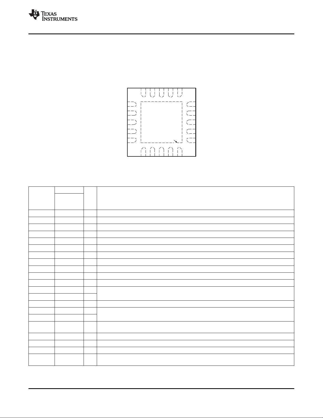
DEVICE INFORMATION
RUK PACKAGE
20 PINS
(TOP VIEW)
PIN FUNCTIONS
PIN NO.
TPS51225
TPS51225B
TPS51225C
Supply input for high-side MOSFET (bootstrap terminal). Connect capacitor from this pin to SW
terminal.
Voltage feedback Input
Power conversion voltage input. Apply the same voltage as drain voltage of high-side MOSFETs of
— — GND terminal, solder to the ground plane
channel 1 and channel 2.
Product Folder Link(s) :TPS51225 TPS51225B TPS51225C
NAME I/O DESCRIPTION
CS1 1 O Sets the channel 1 OCL trip level.
CS2 5 O Sets the channel 2OCL trip level.
DRVH1 16 O High-side driver output
DRVH2 10 O High-side driver output
DRVL1 15 O Low-side driver output
DRVL2 11 O Low-side driver output
EN1 20 I Channel 1 enable.
EN2 6 I Channel 2 enable.
PGOOD 7 O Power good output flag. Open drain output. Pull up to external rail via a resistor
SW1 18 O Switch-node connection.
SW2 8 O Switch-node connection.
VBST1 17 I
VBST2 9 I
VCLK 19 O Clock output for charge pump.
VFB1 2 I
VFB2 4 I
VIN 12 I
VO1 14 I Output voltage input, 5-V input for switch-over.
VREG3 3 O 3.3-V LDO output.
VREG5 13 O 5-V LDO output.
Thermal
pad
Copyright © 2012, Texas Instruments Incorporated Submit Documentation Feedback 7
VIN
VBST1
TPS51225
TPS51225 B
TPS51225 C
DRVH1
SW1
DRVL1
VO1
VFB1
CS1
EN1
VCLK
VREG5
VBST2
DRVH2
SW2
DRVL2
VFB2
CS2
EN2
PGOOD
VREG3
UDG-12002
+ +
+
+
+
155°C/145°C
+
4.5 V/4.0 V
VO_OK
EN
FAULT
REF
PGOOD
DCHG
VIN VDDVDRV
GNDPGND
Switcher
Controller
(CH1)
EN
FAULT
REF
PGOOD
DCHG
VINVDD VDRV
GND PGND
Switcher
Controller
(CH2)
+
2 V
Osc
GND
(Thermal Pad)
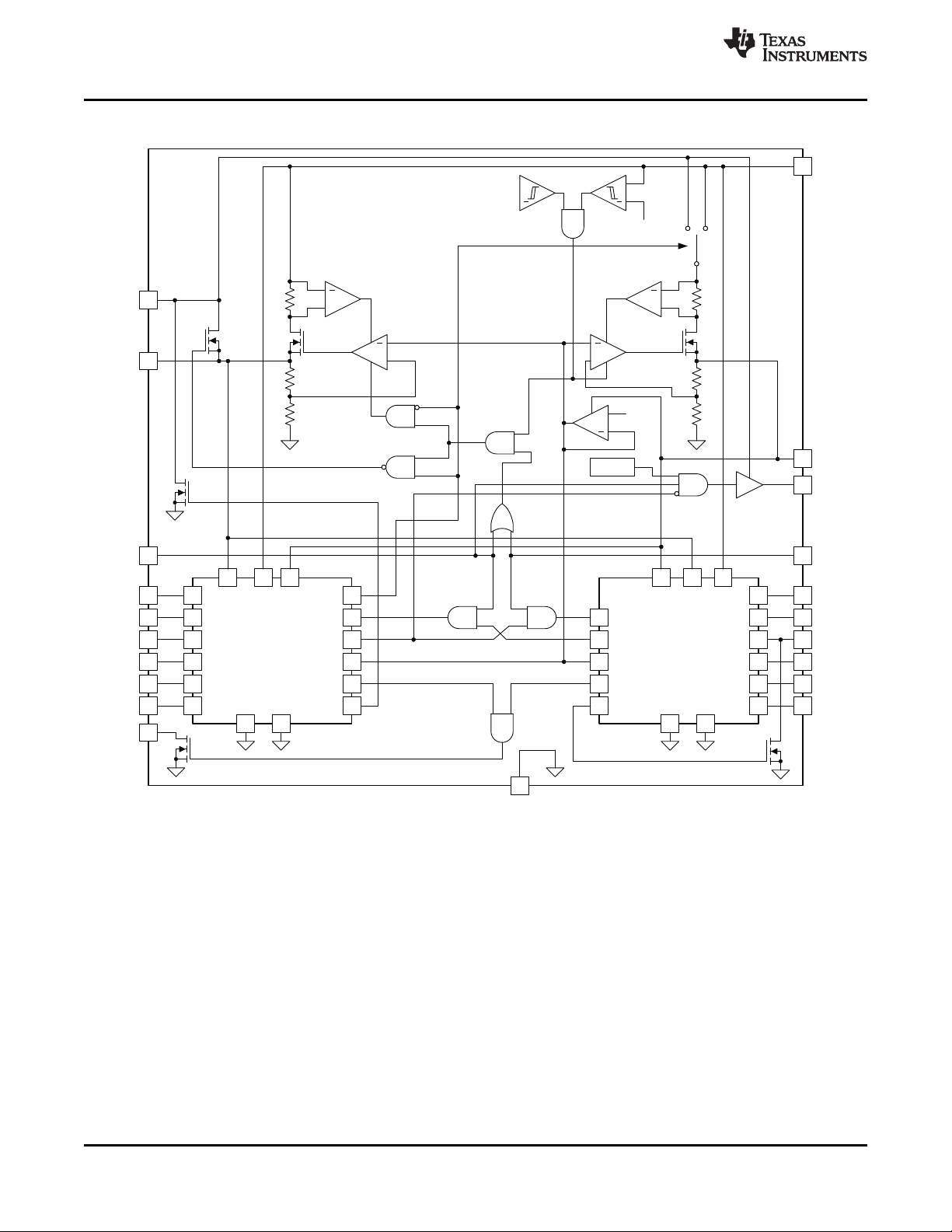
TPS51225, TPS51225B, TPS51225C
SLUSAV0A –JANUARY 2012–REVISED JUNE 2012
FUNCTIONAL BLOCK DIAGRAM (TPS51225/B/C)
www.ti.com
8 Submit Documentation Feedback Copyright © 2012, Texas Instruments Incorporated
Product Folder Link(s) :TPS51225 TPS51225B TPS51225C
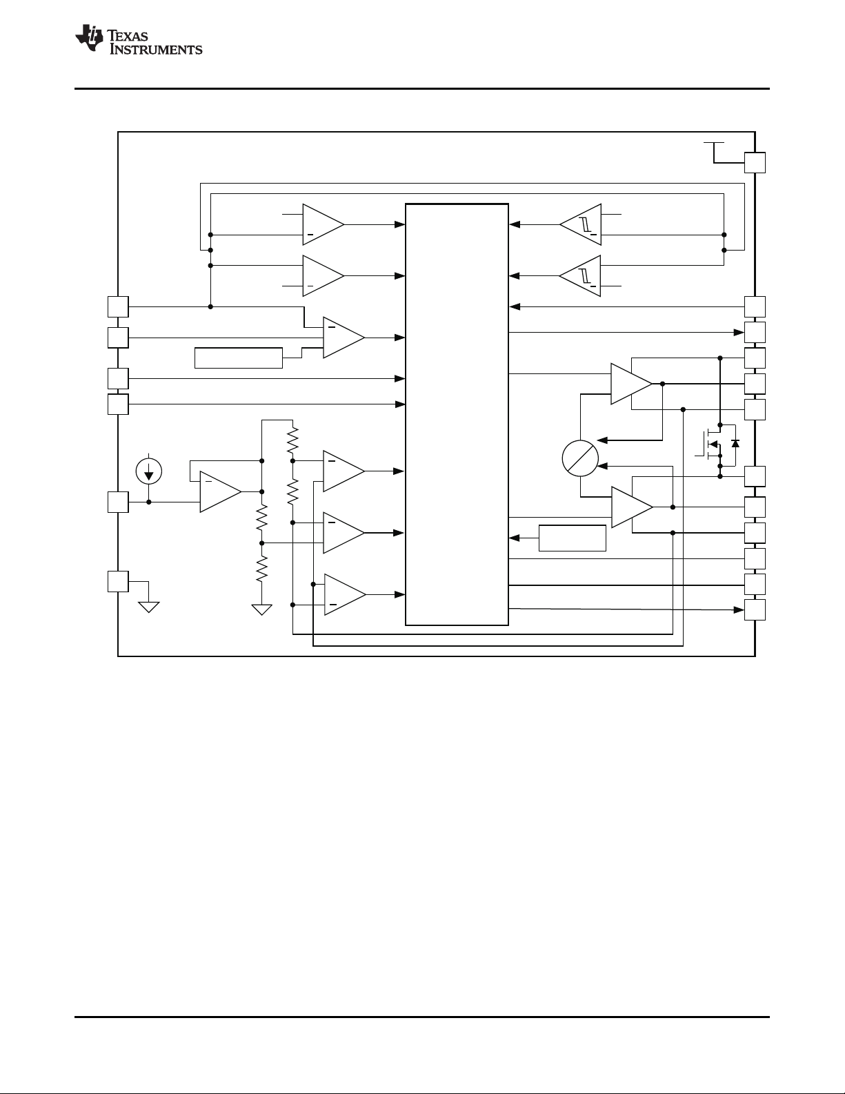
DCHG
SW
TPS51225
TPS51225B
TPS51225C
NOC
ZC
XCON
VO_OK
DRVL
PWM
Control Logic
UDG-12007
+
+
V
REF
+15%
+
+
SKIP
UV
OV
V
REF
–40%
+
VIN
GND
REF
One-Shot
Discharge
10 µA
VBST
DRVH
FAULT
PGOOD
CS
+
VFB
OC
+
+
SS Ramp Comp
V
REF
+5%/10%
V
REF
–5%/10%
+
+
EN
VDD
HS
LS
VDRV
PGND
PGOOD
www.ti.com
SWITCHER CONTROLLER BLOCK DIAGRAM
TPS51225, TPS51225B, TPS51225C
SLUSAV0A –JANUARY 2012–REVISED JUNE 2012
Copyright © 2012, Texas Instruments Incorporated Submit Documentation Feedback 9
Product Folder Link(s) :TPS51225 TPS51225B TPS51225C

( )
( )
- ´
= ´
´ ´
IN OUT OUT
OUT LL
SW IN
V V V
1
I
2 L f V
TPS51225, TPS51225B, TPS51225C
SLUSAV0A –JANUARY 2012–REVISED JUNE 2012
DETAILED DESCRIPTION
PWM Operations
The main control loop of the switch mode power supply (SMPS) is designed as an adaptive on-time pulse width
modulation (PWM) controller. It supports a proprietary D-CAP™ mode. D-CAP™ mode does not require external
conpensation circuit and is suitable for low external component count configuration when used with appropriate
amount of ESR at the output capacitor(s).
At the beginning of each cycle, the synchronous high-side MOSFET is turned on, or enters the ON state. This
MOSFET is turned off, or enters the ‘OFF state, after the internal, one-shot timer expires. The MOSFET is turned
on again when the feedback point voltage, V
, decreased to match the internal 2-V reference. The inductor
VFB
current information is also monitored and should be below the overcurrent threshold to initiate this new cycle. By
repeating the operation in this manner, the controller regulates the output voltage. The synchronous low-side
(rectifying) MOSFET is turned on at the beginning of each OFF state to maintain a minimum of conduction loss.
The low-side MOSFET is turned off before the high-side MOSFET turns on at next switching cycle or when
inductor current information detects zero level. This enables seamless transition to the reduced frequency
operation during light-load conditions so that high efficiency is maintained over a broad range of load current.
Adaptive On-Time/ PWM Frequency Control
Bacause the TPS51225/B/C does not have a dedicated oscillator for control loop on board, switching cycle is
controlled by the adaptive on-time circuit. The on-time is controlled to meet the target switching frequency by
feed-forwarding the input and output voltage into the on-time one-shot timer. The target switching frequency is
varied according to the input voltage to achieve higher duty operation for lower input voltage application. The
switching frequency of CH1 (5-V output) is 300 kHz during continuous conduction mode (CCM) operation when
VIN= 20 V. The CH2 (3.3-V output) is 355 kHz during CCM when VIN= 20 V.
www.ti.com
Light Load Condition in Auto-Skip Operation (TPS51225/C)
The TPS51225/C automatically reduces switching frequency during light-load conditions to maintain high
efficiency. This reduction of frequency is achieved smoothly and without an increase in output voltage ripple. A
more detailed description of this operation is as follows. As the output current decreases from heavy-load
condition, the inductor current is also reduced and eventually approaches valley zero current, which is the
boundary between continuous conduction mode and discontinuous conduction mode. The rectifying MOSFET is
turned off when this zero inductor current is detected. As the load current further decreases, the converter runs in
discontinuous conduction mode and it takes longer and longer to discharge the output capacitor to the level that
requires the next ON cycle. The ON time is maintained the same as that in the heavy-load condition. In reverse,
when the output current increase from light load to heavy load, the switching frequency increases to the preset
value as the inductor current reaches to the continuous conduction. The transition load point to the light load
operation I
OUT(LL)
as shown in Equation 1.
where
• fSWis the PWM switching frequency (1)
Switching frequency versus output current during light-load conditions is a function of inductance (L), input
voltage (VIN) and output voltage (V
I
.
OUT(LL)
(i.e. the threshold between continuous and discontinuous conduction mode) can be calculated
), but it decreases almost proportional to the output current from the
OUT
10 Submit Documentation Feedback Copyright © 2012, Texas Instruments Incorporated
Product Folder Link(s) :TPS51225 TPS51225B TPS51225C

= £
p ´ ´
SW
0
OUT
f
1
f
2 ESR C 4
R1
R2
Voltage
Divider
+
VFB
+
VREF
PWM
Control
Logic
and
Divider
L
ESR
C
OUT
V
C
R
LOAD
I
IND
I
OUT
UDG-12010
I
C
Switching Modulator
Output
Capacitor
V
OUT
TPS51225
TPS51225 B
TPS51225 C
V
IN
DRVH
DRVL
TPS51225, TPS51225B, TPS51225C
www.ti.com
Light-Load Condition in Out-of-Audio™ Operation (TPS51225B)
Out-of-Audio™ (OOA) light-load mode is a unique control feature that keeps the switching frequency above
acoustic audible frequencies toward a virtual no-load condition. During Out-of-Audio™ operation, the OOA
control circuit monitors the states of both MOSFETs and forces them to transition into the ON state if both of
MOSFETs are off for more than 40 μs. When both high-side and low-side MOSFETs are off for 40 µs during a
light-load condition, the operation mode is changed to FCCM. This mode change initiates the low-side MOSFET
on and pulls down the output voltage. Then, the high-side MOSFET is turned on and stops switching again.
Table 1. SKIP Mode Operation (TPS51225/B/C)
SKIP MODE OPERATION
TPS51225 Auto-skip
TPS51225B OOA
TPS51225C Auto-skip
D-CAP™ Mode
From small-signal loop analysis, a buck converter using D-CAP™ mode can be simplified as shown in Figure 1.
SLUSAV0A –JANUARY 2012–REVISED JUNE 2012
The output voltage is compared with internal reference voltage after divider resistors, R1 and R2. The PWM
comparator determines the timing to turn onthe high-side MOSFET. The gain and speed of the comparator is
high enough to keep the voltage at the beginning of each ON cycle substantially constant. For the loop stability,
the 0dB frequency, ƒ0, defined in Equation 2 must be lower than 1/4 of the switching frequency.
As ƒ0is determined solely by the output capacitor characteristics, the loop stability during D-CAP™ mode is
determined by the capacitor chemistry. For example, specialty polymer capacitors have output capacitance in the
order of several hundred micro-Farads and ESR in range of 10 milli-ohms. These yield an f0value on the order
of 100 kHz or less and the loop is stable. However, ceramic capacitors have ƒ0at more than 700 kHz, which is
not suitable for this operational mode.
Copyright © 2012, Texas Instruments Incorporated Submit Documentation Feedback 11
Figure 1. Simplifying the Modulator
Product Folder Link(s) :TPS51225 TPS51225B TPS51225C
(2)

VIN-UVLO_threshold
EN_threshold
95% of V
OUT
95% of Vout
EN_threshold
VIN
VREG3
EN1
VREG5
5-V V
OUT
PGOOD
EN2
Soft-Start Time (tSS)
Soft-Start Time
(t
SS(ramp)
)
Soft-Start Time (tSS)
Soft-Start Time
(t
SS(ramp)
)
PGOOD
Delay
t
PGDEL
3.3-V V
OUT
UDG-12013
VREG5-UVLO_threshold
TPS51225, TPS51225B, TPS51225C
SLUSAV0A –JANUARY 2012–REVISED JUNE 2012
Enable and Powergood
VREG3 is an always-on regulator (TPS51225/B), VREG3/VREG5 are always-on regulators (TPS51225C), when
the input voltage is beyond the UVLO threshold it turns ON. VREG5 is turned ON when either EN1 or EN2
enters the ON state. The VCLK signal initiates when EN1 enters the ON state (TPS51225/B/C). Enable states
are shown in Table 2 through Table 3.
Table 2. Enabling/PGOOD State (TPS51225/B)
EN1 EN2 VREG5 VREG3 CH1 (5Vout) CH2 (3.3Vout) VCLK PGOOD
OFF OFF OFF ON OFF OFF OFF Low
ON OFF ON ON ON OFF ON Low
OFF ON ON ON OFF ON OFF Low
ON ON ON ON ON ON ON High
Table 3. Enabling/PGOOD State (TPS51225C)
EN1 EN2 VREG5 VREG3 CH1 (5Vout) CH2 (3.3Vout) VCLK PGOOD
OFF OFF ON ON OFF OFF OFF Low
ON OFF ON ON ON OFF ON Low
OFF ON ON ON OFF ON OFF Low
ON ON ON ON ON ON ON High
www.ti.com
12 Submit Documentation Feedback Copyright © 2012, Texas Instruments Incorporated
Figure 2. TPS51225 and TPS51225B Timing
Product Folder Link(s) :TPS51225 TPS51225B TPS51225C

VIN-UVLO_threshold
95% of V
OUT
95% of Vout
EN_threshold
VIN
VREG3
VREG5
5-V V
OUT
PGOOD
EN2
Soft-Start Time (tSS)
Soft-Start Time
(t
SS(ramp)
)
Soft-Start Time (tSS)
Soft-Start Time
(t
SS(ramp)
)
PGOOD
Delay
t
PGDEL
3.3-V V
OUT
UDG-12015
EN_threshold
EN1
2.4 V
www.ti.com
TPS51225, TPS51225B, TPS51225C
SLUSAV0A –JANUARY 2012–REVISED JUNE 2012
Figure 3. TPS51225C Timing
Copyright © 2012, Texas Instruments Incorporated Submit Documentation Feedback 13
Product Folder Link(s) :TPS51225 TPS51225B TPS51225C

( )
( )
( )
( )IND ripple
IN OUT OUT
TRIP TRIP
OCP
SW IN
DS on DS on
I
V V V
V V
1
I
R 2 R 2 L f V
- ´
= + = + ´
´ ´
CS CS
TRIP
R I
V 1 mV
8
´
= +
TPS51225, TPS51225B, TPS51225C
SLUSAV0A –JANUARY 2012–REVISED JUNE 2012
Soft-Start and Discharge
The TPS51225/B/C operates an internal, 0.8-ms, voltage servo soft-start for each channel. When the ENx pin
becomes higher than the enable threshold voltage, an internal DAC begins ramping up the reference voltage to
the PWM comparator. Smooth control of the output voltage is maintained during start-up. When ENx becomes
lower than the lower level of threshold voltage, TPS51225/B/C discharges outputs using internal MOSFETs
through VO1 (CH1) and SW2 (CH2).
VREG5/VREG3 Linear Regulators
There are two sets of 100-mA standby linear regulators which output 5 V and 3.3 V, respectively. The VREG5
pin provides the current for the gate drivers. The VREG3 pin functions as the main power supply for the analog
circuitry of the device. VREG3 is an Always ON LDO and TPS51225C has Always ON VREG5. (see )
Add ceramic capacitors with a value of 1 µF or larger (X5R grade or better) placed close to the VREG5 and
VREG3 pins to stabilize LDOs.
The VREG5 pin switchover function is asserted when three conditions are present:
• CH1 internal PGOOD is high
• CH1 is not in OCL condition
• VO1 voltage is higher than VREG5-1V
In this switchover condition, three things occur:
• the internal 5-V, LDO regulator is shut off
• the VREG5 output is connected to VO1 by internal switchover MOSFET
• VREG3 input pass is changed from VIN to VO1
www.ti.com
VCLK for Charge Pump
The 260-kHz VCLK signal can be used in the charge pump circuit. The VCLK signal becomes available when
EN1. The VCLK driver is driven by VO1 voltage. In a design that does not require VCLK output, leave the VCLK
pin open.
Overcurrent Protection
TPS51225/B/C has cycle-by-cycle over current limiting control. The inductor current is monitored during the OFF
state and the controller maintains the OFF state during the inductor current is larger than the overcurrent trip
level. In order to provide both good accuracy and cost effective solution, TPS51225/B/C supports temperature
compensated MOSFET R
setting resistor, RCS. The CSx pin sources CS current (ICS) which is 10 µA typically at room temperature, and the
CSx terminal voltage (VCS= RCS× ICS) should be in the range of 0.2 V to 2 V over all operation temperatures.
The trip level is set to the OCL trip voltage (V
The inductor current is monitored by the voltage between GND pin and SWx pin so that SWx pin should be
connected to the drain terminal of the low-side MOSFET properly.The CS pin current has a 4500 ppm/°C
temperature slope to compensate the temperature dependency of the R
current sensing node so that GND should be connected to the source terminal of the low-side MOSFET.
As the comparison is done during the OFF state, V
current at the overcurrent threshold, I
In an overcurrent condition, the current to the load exceeds the current to the output capacitor thus the output
voltage tends to fall down. Eventually, it ends up with crossing the undervoltage protection threshold and
shutdown both channels.
sensing. The CSx pin should be connected to GND through the CS voltage
DS(on)
) as shown in Equation 3.
TRIP
. GND is used as the positive
DS(on)
sets the valley level of the inductor current. Thus, the load
, can be calculated as shown in Equation 4.
OCP
TRIP
(3)
(4)
14 Submit Documentation Feedback Copyright © 2012, Texas Instruments Incorporated
Product Folder Link(s) :TPS51225 TPS51225B TPS51225C

TPS51225, TPS51225B, TPS51225C
www.ti.com
Output Overvoltage/Undervoltage Protection
TPS51225/B/C asserts the overvoltage protection (OVP) when VFBx voltage reaches OVP trip threshold level.
When an OVP event is detected, the controller changes the output target voltage to 0 V. This usually turns off
DRVH and forces DRVL to be on. When the inductor current begins to flow through the low-side MOSFET and
reaches the negative OCL, DRVL is turned off and DRVH is turned on. After the on-time expires, DRVH is turned
off and DRVL is turned on again. This action minimizes the output node undershoot due to LC resonance. When
the VFBx reaches 0V, the driver output is latched as DRVH off, DRVL on. The undervoltage protection (UVP)
latch is set when the VFBx voltage remains lower than UVP trip threshold voltage for 250 µs or longer. In this
fault condition, the controller latches DRVH low and DRVL low and discharges the outputs. UVP detection
function is enabled after 1.35 ms of SMPS operation to ensure startup.
Undervoltage Lockout (UVLO) Protection
TPS51225/B/C has undervoltage lock out protection at VIN, VREG5 and VREG3. When each voltage is lower
than their UVLO threshold voltage, both SMPS are shut-off. They are non-latch protections.
Over-Temperature Protection
TPS51225/B/C features an internal temperature monitor. If the temperature exceeds the threshold value
(typically 155°C), TPS51225/B/C is shut off including LDOs. This is non-latch protection.
SLUSAV0A –JANUARY 2012–REVISED JUNE 2012
Copyright © 2012, Texas Instruments Incorporated Submit Documentation Feedback 15
Product Folder Link(s) :TPS51225 TPS51225B TPS51225C

V
VOUT
V
REF
(2)
t
ON
t
OFF
Slope (2)
Jitter
20 mV
Slope (1)
Jitter
UDG-12012
V
REF
+Noise
(1)
( )
OUT SW
IND ripple
V 20 mV (1 D) 20 mV L f
ESR
2 V I 2 V
´ ´ - ´ ´
= =
´
( )
( )
( )
(
)
( )
IN OUT OUT
max
TRIP
IND peak
SW IN
DS on max
V V V
V
1
I
R L f V
- ´
= + ´
´
( )
( )
(
)
( ) ( )
( )
(
)
- ´ - ´
= ´ = ´
´ ´
IN OUT OUT IN OUT OUT
max max
SW IN OUT SW IN(max)
IND ripple max max
V V V V V V
1 3
L
I f V I f V
( )
OUT RIPPLE
V 0.5 V 2.0
R1 R2
2.0
- ´ -
= ´
TPS51225, TPS51225B, TPS51225C
SLUSAV0A –JANUARY 2012–REVISED JUNE 2012
External Components Selection
The external components selection is relatively simple for a design using D-CAP™ mode.
Step 1. Determine the Value of R1 and R2
The recommended R2 value is between 10 kΩ and 20 kΩ. Determine R1 using Equation 5.
Step 2. Choose the Inductor
The inductance value should be determined to give the ripple current of approximately 1/3 of maximum output
current. Larger ripple current increases output ripple voltage, improves signal:noise ratio, and helps ensure stable
operation.
The inductor also needs to have low DCR to achieve good efficiency, as well as enough room above peak
inductor current before saturation. The peak inductor current can be estimated as shown in Equation 7.
www.ti.com
(5)
(6)
(7)
Step 3. Choose Output Capacitor(s)
Organic semiconductor capacitor(s) or specialty polymer capacitor(s) are recommended. Determine ESR to meet
required ripple voltage above. A quick approximation is as shown in Equation 8.
where
• D as the duty-cycle factor
• the required output ripple voltage slope is approximately 20 mV per tSW(switching period) in terms of VFB
terminal (8)
16 Submit Documentation Feedback Copyright © 2012, Texas Instruments Incorporated
Figure 4. Ripple Voltage Slope and Jitter Performance
Product Folder Link(s) :TPS51225 TPS51225B TPS51225C

TPS51225, TPS51225B, TPS51225C
www.ti.com
Layout Considerations
Good layout is essential for stable power supply operation. Follow these guidelines for an efficient PCB layout.
Placement
• Place voltage setting resistors close to the device pins.
• Place bypass capacitors for VREG5 and VREG3 close to the device pins.
Routing (Sensitive analog portion)
• Use small copper space for VFBx. There are short and narrow traces to avoid noise coupling.
• Connect VFB resistor trace to the positive node of the output capacitor. Routing inner layer away from power
traces is recommended.
• Use short and wide trace from VFB resistor to vias to GND (internal GND plane).
Routing (Power portion)
• Use wider/shorter traces of DRVL for low-side gate drivers to reduce stray inductance.
• Use the parallel traces of SW and DRVH for high-side MOSFET gate drive in a same layer or on adjoin
layers, and keep them away from DRVL.
• Use wider/ shorter traces between the source terminal of the high-side MOSFET and the drain terminal of the
low-side MOSFET
• Thermal pad is the GND terminal of this device. Five or more vias with 0.33-mm (13-mils) diameter connected
from the thermal pad to the internal GND plane should be used to have strong GND connection and help heat
dissipation.
SLUSAV0A –JANUARY 2012–REVISED JUNE 2012
Copyright © 2012, Texas Instruments Incorporated Submit Documentation Feedback 17
Product Folder Link(s) :TPS51225 TPS51225B TPS51225C

0
2
4
6
8
10
12
14
16
18
20
−40 −25 −10 5 20 35 50 65 80 95 110 125
Junction Temperature (°C)
CS Source Current (µA)
G005
210
220
230
240
250
260
270
280
290
300
310
−40 −25 −10 5 20 35 50 65 80 95 110 125
Junction Temperature (°C)
VCLK Frequency (kHz)
G006
0.0
0.2
0.4
0.6
0.8
1.0
1.2
1.4
1.6
−40 −25 −10 5 20 35 50 65 80 95 110 125
Junction Temperature (°C)
VO1 Supply Current 1 (mA)
G003
0
50
100
150
200
250
300
−40 −25 −10 5 20 35 50 65 80 95 110 125
Junction Temperature (°C)
VIN Stand−By Current (µA)
TPS51225C Only
G004
0.0
0.2
0.4
0.6
0.8
1.0
1.2
1.4
1.6
−40 −25 −10 5 20 35 50 65 80 95 110 125
Junction Temperature (°C)
VIN Supply Current 1 (mA)
G001
0
10
20
30
40
50
60
−40 −25 −10 5 20 35 50 65 80 95 110 125
Junction Temperature (°C)
VIN Supply Current 2 (µA)
G002
TPS51225, TPS51225B, TPS51225C
SLUSAV0A –JANUARY 2012–REVISED JUNE 2012
TYPICAL CHARACTERISTICS
Figure 5. VIN Supply Current 1 vs. Junction Temperature Figure 6. VIN Supply Current 2 vs. Junction Temperature
www.ti.com
Figure 7. VO1 Supply Current 1 vs. Junction Temperature Figure 8. VIN Stand-By Current vs. Junction Temperature
Figure 9. CS Source Current vs. Junction Temperature Figure 10. Clock Frequency vs. Junction Temperature
18 Submit Documentation Feedback Copyright © 2012, Texas Instruments Incorporated
Product Folder Link(s) :TPS51225 TPS51225B TPS51225C

20
30
40
50
60
70
80
90
100
0.001 0.01 0.1 1 10
Output Current (A)
Efficiency (%)
V
VIN
= 8 V
V
VIN
= 12 V
V
VIN
= 20 V
Auto−Skip
V
VOUT
= 3.3 V
G010
0
10
20
30
40
50
60
70
80
90
100
0.001 0.01 0.1 1 10
Output Current (A)
Efficiency (%)
V
VIN
= 8 V
V
VIN
= 12 V
V
VIN
= 20 V
Out−of_Audio
V
VOUT
= 3.3 V
G011
4.85
4.90
4.95
5.00
5.05
5.10
5.15
0.001 0.01 0.1 1 10
Output Current (A)
Output Volage (V)
V
VIN
= 8 V
V
VIN
= 12 V
V
VIN
= 20 V
Auto−Skip
V
VOUT
= 5 V
G014
4.85
4.90
4.95
5.00
5.05
5.10
5.15
0.001 0.01 0.1 1 10
Output Current (A)
Output Volage (V)
V
VIN
= 8 V
V
VIN
= 12 V
V
VIN
= 20 V
Out−of−Audio
V
VOUT
= 5 V
G015
40
50
60
70
80
90
100
0.001 0.01 0.1 1 10
Output Current (A)
Efficiency (%)
V
VIN
= 8 V
V
VIN
= 12 V
V
VIN
= 20 V
Auto−Skip
V
VOUT
= 5 V
G007
0
10
20
30
40
50
60
70
80
90
100
0.001 0.01 0.1 1 10
Output Current (A)
Efficiency (%)
V
VIN
= 8 V
V
VIN
= 12 V
V
VIN
= 20 V
Out−of−Audio
V
VOUT
= 5 V
G008
www.ti.com
TPS51225, TPS51225B, TPS51225C
SLUSAV0A –JANUARY 2012–REVISED JUNE 2012
TYPICAL CHARACTERISTICS (continued)
Figure 11. Efficiency vs. Output Current Figure 12. Efficiency vs. Output Current
Figure 13. Load Regulation Figure 14. Load Regulation
Figure 15. Efficiency vs. Output Current Figure 16. Efficiency vs. Output Current
Copyright © 2012, Texas Instruments Incorporated Submit Documentation Feedback 19
Product Folder Link(s) :TPS51225 TPS51225B TPS51225C

0
50
100
150
200
250
300
350
400
450
0.001 0.01 0.1 1 10
Output Current (A)
Switching Frequency (kHz)
V
VIN
= 8 V
V
VIN
= 12 V
V
VIN
= 20 V
Auto−Skip
V
VOUT
= 3.3 V
G018
0
50
100
150
200
250
300
350
400
450
0.001 0.01 0.1 1 10
Output Current (A)
Switching Frequency (kHz)
V
VIN
= 8 V
V
VIN
= 12 V
V
VIN
= 20 V
Out−of−Audio
V
VOUT
= 3.3 V
G019
0
50
100
150
200
250
300
350
0.001 0.01 0.1 1 10
Output Current (A)
Switching Frequency (kHz)
V
VIN
= 8 V
V
VIN
= 12 V
V
VIN
= 20 V
Auto−Skip
V
VOUT
= 5 V
G016
0
50
100
150
200
250
300
350
0.001 0.01 0.1 1 10
Output Current (A)
Switching Frequency (kHz)
V
VIN
= 8 V
V
VIN
= 12 V
V
VIN
= 20 V
Out−of−Audio
V
VOUT
= 5 V
G017
3.23
3.28
3.33
3.38
3.43
0.001 0.01 0.1 1 10
Output Current (A)
Output Volage (V)
V
VIN
= 8 V
V
VIN
= 12 V
V
VIN
= 20 V
Auto−skip
V
VOUT
= 3.3 V
G012
3.23
3.28
3.33
3.38
3.43
0.001 0.01 0.1 1 10
Output Current (A)
Output Volage (V)
V
VIN
= 8 V
V
VIN
= 12 V
V
VIN
= 20 V
Out−of−Audio
V
VOUT
= 3.3 V
G013
TPS51225, TPS51225B, TPS51225C
SLUSAV0A –JANUARY 2012–REVISED JUNE 2012
TYPICAL CHARACTERISTICS (continued)
Figure 17. Load Regulation Figure 18. Load Regulation
www.ti.com
Figure 19. Switching Frequency vs. Output Current Figure 20. Switching Frequency vs. Output Current
Figure 21. Switching Frequency vs. Output Current Figure 22. Switching Frequency vs. Output Current
20 Submit Documentation Feedback Copyright © 2012, Texas Instruments Incorporated
Product Folder Link(s) :TPS51225 TPS51225B TPS51225C

0
50
100
150
200
250
300
350
400
450
500
5 10 15 20 25
Input Voltage (V)
Switching Frequency (kHz)
V
OUT
= 5 V
I
OUT
= 6 A
G000
0
50
100
150
200
250
300
350
400
450
500
5 10 15 20 25
Input Voltage (V)
Switching Frequency (kHz)
V
OUT
= 3.3 V
I
OUT
= 6 A
G000
Time (100 µs /div)
V
VIN
= 12 V
I
OUT
3A ßà 8 A
V
OUT1
(50 mV/div)
SW1 (10 V/div)
V
OUT2
0 A( 50 mV/div)
I
IND1
(5 A/div)
V
VIN
= 12 V
I
OUT
3A ßà 8 A
V
OUT1
(50 mV/div)
SW1 (10 V/div)
V
OUT2
0 A ( 50 mV/div )
Time (100 µs /div)
I
IND1
(5 A/div)
V
OUT1
(2 V/div)
PGOOD (5 V/div)
V
OUT2
(2 V/div)
Time (400 µs/div)
EN1 = EN2 (5 V/div)
V
OUT1
(2 V/div)
EN1 = EN2 (5 V/div)
V
OUT2
(2 V/div)
PGOOD (5 V/div)
Time (10 ms/div)
www.ti.com
TPS51225, TPS51225B, TPS51225C
SLUSAV0A –JANUARY 2012–REVISED JUNE 2012
TYPICAL CHARACTERISTICS (continued)
Figure 23. Start-Up Figure 24. Output Discharge
Figure 25. 5-V Load Transient Figure 26. 3.3-V Load Transient
Copyright © 2012, Texas Instruments Incorporated Submit Documentation Feedback 21
Figure 27. Switching Frequency vs. Input Voltage Figure 28. Switching Frequency vs. Input Voltage
Product Folder Link(s) :TPS51225 TPS51225B TPS51225C

VIN
VBST1
U1
TPS51225
TPS51225 B
TPS51225 C
DRVH1
SW1
12
17
16
18
0.1 µF
L1
C1
15.3 kW
DRVL115
VO114
VFB1
2
CS1
1
EN1
20
51 kW
10 kW
EN 5V
0.1 µF
0.1 µF
VCLK19
VREG513
10 µF x 2
V
IN
V
OUT
5 V-8A
Charge-pump
Output
VBST2
DRVH2
SW2
9
10
8
DRVL2
11
VFB2
4
CS2
5
EN2
6
PGOOD
7
VREG3
3
10 µF x 2
0.1 µF
L2
C2
6.57 k W
47 kW
10 kW
EN 3.3 V
1 µF
V
OUT
3.3 V - 8A
PGOOD
VREG
(3.3-V LDO)
UDG-12008
2.2 W
Q2
Q4
2.2 W
Q1
Q3
0.1 µF
GND
0.1 µF
VREG5
(5-V LDO)
1 µF
D1
TPS51225, TPS51225B, TPS51225C
SLUSAV0A –JANUARY 2012–REVISED JUNE 2012
APPLICATION DIAGRAM (TPS51225/TPS51225B/TPS51225C)
www.ti.com
Table 4. Key External Components (APPLICATION DIAGRAM (TPS51225/TPS51225B/TPS51225C))
REFERENCE
DESIGNATOR
L1 Output Inductor (5-V
L2 Output Inductor (3.3-V
C1 Output Capacitor (5-V
C2 Output Capacitor (3.3-V
Q1 High-side MOSFET (5-V
Q2 High-side MOSFET (3.3-V
Q3 Low-side MOSFET (5-V
Q4 Low-side MOSFET (3.3-V
22 Submit Documentation Feedback Copyright © 2012, Texas Instruments Incorporated
FUNCTION MANUFACTURER PART NUMBER
) Toko FDVE1040-3R3M
OUT
) Toko FDVE1040-2R2M
OUT
) SANYO 6TPE330MIL x 2
OUT
) SANYO 4TPE470MIL
OUT
) Fairchild FDMC7692
OUT
) Fairchild FDMC7692
OUT
) Fairchild FDMC7672
OUT
) Fairchild FDMC7672
OUT
Product Folder Link(s) :TPS51225 TPS51225B TPS51225C

TPS51225, TPS51225B, TPS51225C
www.ti.com
Changes from Original (January 2012) to Revision A Page
• Deleted references to obsolete option TPS51225A throughout document .......................................................................... 1
SLUSAV0A –JANUARY 2012–REVISED JUNE 2012
Copyright © 2012, Texas Instruments Incorporated Submit Documentation Feedback 23
Product Folder Link(s) :TPS51225 TPS51225B TPS51225C

PACKAGE OPTION ADDENDUM
www.ti.com
19-May-2012
PACKAGING INFORMATION
Orderable Device
TPS51225BRUKR ACTIVE QFN RUK 20 3000 Green (RoHS
TPS51225BRUKT ACTIVE QFN RUK 20 250 Green (RoHS
TPS51225CRUKR ACTIVE QFN RUK 20 3000 Green (RoHS
TPS51225CRUKT ACTIVE QFN RUK 20 250 Green (RoHS
TPS51225RUKR ACTIVE QFN RUK 20 3000 Green (RoHS
TPS51225RUKT ACTIVE QFN RUK 20 250 Green (RoHS
(1)
The marketing status values are defined as follows:
ACTIVE: Product device recommended for new designs.
LIFEBUY: TI has announced that the device will be discontinued, and a lifetime-buy period is in effect.
NRND: Not recommended for new designs. Device is in production to support existing customers, but TI does not recommend using this part in a new design.
PREVIEW: Device has been announced but is not in production. Samples may or may not be available.
OBSOLETE: TI has discontinued the production of the device.
Status
(1)
Package Type Package
Drawing
Pins Package Qty
Eco Plan
& no Sb/Br)
& no Sb/Br)
& no Sb/Br)
& no Sb/Br)
& no Sb/Br)
& no Sb/Br)
(2)
Lead/
Ball Finish
CU NIPDAU Level-2-260C-1 YEAR
CU NIPDAU Level-2-260C-1 YEAR
CU NIPDAU Level-2-260C-1 YEAR
CU NIPDAU Level-2-260C-1 YEAR
CU NIPDAU Level-2-260C-1 YEAR
CU NIPDAU Level-2-260C-1 YEAR
MSL Peak Temp
(3)
Samples
(Requires Login)
(2)
Eco Plan - The planned eco-friendly classification: Pb-Free (RoHS), Pb-Free (RoHS Exempt), or Green (RoHS & no Sb/Br) - please check http://www.ti.com/productcontent for the latest availability
information and additional product content details.
TBD: The Pb-Free/Green conversion plan has not been defined.
Pb-Free (RoHS): TI's terms "Lead-Free" or "Pb-Free" mean semiconductor products that are compatible with the current RoHS requirements for all 6 substances, including the requirement that
lead not exceed 0.1% by weight in homogeneous materials. Where designed to be soldered at high temperatures, TI Pb-Free products are suitable for use in specified lead-free processes.
Pb-Free (RoHS Exempt): This component has a RoHS exemption for either 1) lead-based flip-chip solder bumps used between the die and package, or 2) lead-based die adhesive used between
the die and leadframe. The component is otherwise considered Pb-Free (RoHS compatible) as defined above.
Green (RoHS & no Sb/Br): TI defines "Green" to mean Pb-Free (RoHS compatible), and free of Bromine (Br) and Antimony (Sb) based flame retardants (Br or Sb do not exceed 0.1% by weight
in homogeneous material)
(3)
MSL, Peak Temp. -- The Moisture Sensitivity Level rating according to the JEDEC industry standard classifications, and peak solder temperature.
Important Information and Disclaimer:The information provided on this page represents TI's knowledge and belief as of the date that it is provided. TI bases its knowledge and belief on information
provided by third parties, and makes no representation or warranty as to the accuracy of such information. Efforts are underway to better integrate information from third parties. TI has taken and
continues to take reasonable steps to provide representative and accurate information but may not have conducted destructive testing or chemical analysis on incoming materials and chemicals.
TI and TI suppliers consider certain information to be proprietary, and thus CAS numbers and other limited information may not be available for release.
Addendum-Page 1

PACKAGE OPTION ADDENDUM
www.ti.com
In no event shall TI's liability arising out of such information exceed the total purchase price of the TI part(s) at issue in this document sold by TI to Customer on an annual basis.
19-May-2012
Addendum-Page 2

PACKAGE MATERIALS INFORMATION
www.ti.com 19-May-2012
TAPE AND REEL INFORMATION
*All dimensions are nominal
Device Package
TPS51225BRUKR QFN RUK 20 3000 330.0 12.4 3.3 3.3 1.1 8.0 12.0 Q2
TPS51225BRUKT QFN RUK 20 250 180.0 12.4 3.3 3.3 1.1 8.0 12.0 Q2
TPS51225CRUKR QFN RUK 20 3000 330.0 12.4 3.3 3.3 1.1 8.0 12.0 Q2
TPS51225CRUKT QFN RUK 20 250 180.0 12.4 3.3 3.3 1.1 8.0 12.0 Q2
TPS51225RUKR QFN RUK 20 3000 330.0 12.4 3.3 3.3 1.1 8.0 12.0 Q2
TPS51225RUKT QFN RUK 20 250 180.0 12.4 3.3 3.3 1.1 8.0 12.0 Q2
Type
Package
Drawing
Pins SPQ Reel
Diameter
(mm)
Reel
Width
W1 (mm)
A0
(mm)B0(mm)K0(mm)P1(mm)W(mm)
Pin1
Quadrant
Pack Materials-Page 1

PACKAGE MATERIALS INFORMATION
www.ti.com 19-May-2012
*All dimensions are nominal
Device Package Type Package Drawing Pins SPQ Length (mm) Width (mm) Height (mm)
TPS51225BRUKR QFN RUK 20 3000 346.0 346.0 29.0
TPS51225BRUKT QFN RUK 20 250 210.0 185.0 35.0
TPS51225CRUKR QFN RUK 20 3000 346.0 346.0 29.0
TPS51225CRUKT QFN RUK 20 250 210.0 185.0 35.0
TPS51225RUKR QFN RUK 20 3000 346.0 346.0 29.0
TPS51225RUKT QFN RUK 20 250 210.0 185.0 35.0
Pack Materials-Page 2


IMPORTANT NOTICE
Texas Instruments Incorporated and its subsidiaries (TI) reserve the right to make corrections, modifications, enhancements, improvements,
and other changes to its products and services at any time and to discontinue any product or service without notice. Customers should
obtain the latest relevant information before placing orders and should verify that such information is current and complete. All products are
sold subject to TI’s terms and conditions of sale supplied at the time of order acknowledgment.
TI warrants performance of its hardware products to the specifications applicable at the time of sale in accordance with TI’s standard
warranty. Testing and other quality control techniques are used to the extent TI deems necessary to support this warranty. Except where
mandated by government requirements, testing of all parameters of each product is not necessarily performed.
TI assumes no liability for applications assistance or customer product design. Customers are responsible for their products and
applications using TI components. To minimize the risks associated with customer products and applications, customers should provide
adequate design and operating safeguards.
TI does not warrant or represent that any license, either express or implied, is granted under any TI patent right, copyright, mask work right,
or other TI intellectual property right relating to any combination, machine, or process in which TI products or services are used. Information
published by TI regarding third-party products or services does not constitute a license from TI to use such products or services or a
warranty or endorsement thereof. Use of such information may require a license from a third party under the patents or other intellectual
property of the third party, or a license from TI under the patents or other intellectual property of TI.
Reproduction of TI information in TI data books or data sheets is permissible only if reproduction is without alteration and is accompanied
by all associated warranties, conditions, limitations, and notices. Reproduction of this information with alteration is an unfair and deceptive
business practice. TI is not responsible or liable for such altered documentation. Information of third parties may be subject to additional
restrictions.
Resale of TI products or services with statements different from or beyond the parameters stated by TI for that product or service voids all
express and any implied warranties for the associated TI product or service and is an unfair and deceptive business practice. TI is not
responsible or liable for any such statements.
TI products are not authorized for use in safety-critical applications (such as life support) where a failure of the TI product would reasonably
be expected to cause severe personal injury or death, unless officers of the parties have executed an agreement specifically governing
such use. Buyers represent that they have all necessary expertise in the safety and regulatory ramifications of their applications, and
acknowledge and agree that they are solely responsible for all legal, regulatory and safety-related requirements concerning their products
and any use of TI products in such safety-critical applications, notwithstanding any applications-related information or support that may be
provided by TI. Further, Buyers must fully indemnify TI and its representatives against any damages arising out of the use of TI products in
such safety-critical applications.
TI products are neither designed nor intended for use in military/aerospace applications or environments unless the TI products are
specifically designated by TI as military-grade or "enhanced plastic." Only products designated by TI as military-grade meet military
specifications. Buyers acknowledge and agree that any such use of TI products which TI has not designated as military-grade is solely at
the Buyer's risk, and that they are solely responsible for compliance with all legal and regulatory requirements in connection with such use.
TI products are neither designed nor intended for use in automotive applications or environments unless the specific TI products are
designated by TI as compliant with ISO/TS 16949 requirements. Buyers acknowledge and agree that, if they use any non-designated
products in automotive applications, TI will not be responsible for any failure to meet such requirements.
Following are URLs where you can obtain information on other Texas Instruments products and application solutions:
Products Applications
Audio www.ti.com/audio Automotive and Transportation www.ti.com/automotive
Amplifiers amplifier.ti.com Communications and Telecom www.ti.com/communications
Data Converters dataconverter.ti.com Computers and Peripherals www.ti.com/computers
DLP® Products www.dlp.com Consumer Electronics www.ti.com/consumer-apps
DSP dsp.ti.com Energy and Lighting www.ti.com/energy
Clocks and Timers www.ti.com/clocks Industrial www.ti.com/industrial
Interface interface.ti.com Medical www.ti.com/medical
Logic logic.ti.com Security www.ti.com/security
Power Mgmt power.ti.com Space, Avionics and Defense www.ti.com/space-avionics-defense
Microcontrollers microcontroller.ti.com Video and Imaging www.ti.com/video
RFID www.ti-rfid.com
OMAP Mobile Processors www.ti.com/omap
Wireless Connectivity www.ti.com/wirelessconnectivity
TI E2E Community Home Page e2e.ti.com
Mailing Address: Texas Instruments, Post Office Box 655303, Dallas, Texas 75265
Copyright © 2012, Texas Instruments Incorporated
 Loading...