

1
2
3
4
24
23
22
21
DRVH2
VIN
VREG3
EN2
DRVH1
V5SW
RF
EN1
TPS51220RHB
(QFN32)
5
6
7
8
20
19
18
17
PGOOD2
SKIPSEL2
CSP2
CSN2
PGOOD1
SKIPSEL1
CSP1
CSN1
9
VFB1
32
SW1
31
VBST1
30
DRVL1
29
VREG5
28
GND
27
DRVL2
26
VBST2
25
SW2
10
COMP111FUNC12EN13VREF214TRIP15COMP216VFB2
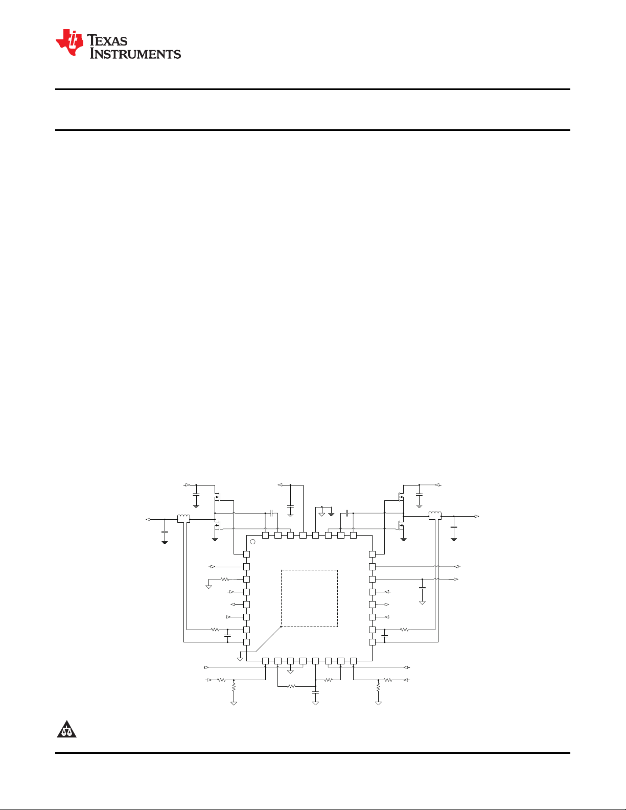
VO1
5.0V
L1
C22
VBAT
PowerPAD
C02
C01
VREG5
5V/100mA
R23
R13
C11
R11
PGOOD1
EN
EN1
VREG3
3.3V/10mA
Q11
Q12
Q22
Q21
C13
R12
GND
R14
GND
GND
GND
L2
R24
GND
C23
C21
R21
R22
GND
PGOOD2
EN2
VO2
3.3V
C03
R01
PGND
GND
SKIPSEL1 SKIPSEL2
VBAT
VO2
C12
VBAT
VO1
VO1
VREG5
C14
PGND
PGND
PGND
PGND
PGND
PGND PGND
C24
GND
TPS51220
www.ti.com
SLVS785C –OCTOBER 2007–REVISED JULY 2009
Fixed Frequency, 99% Duty Cycle Peak Current Mode Notebook System Power Controller
Check for Samples: TPS51220
1
FEATURES
2
• Input Voltage Range: 4.5 V to 28 V
• Output Voltage Range: 1 V to 12 V • OCL/OVP/UVP/UVLO Protections
• Selectable Light Load Operation
(Continuous / Auto Skip / Out-Of-Audio™ Skip) • Thermal Shutdown (Non-Latch)
• Programmable Droop Compensation • Output Discharge Function (Disable Option)
• Voltage Servo Adjustable Soft Start • Integrated Boot Strap MOSFET Switch
• 200 kHz to 1 MHz Fixed Frequency PWM • QFN-32 (RHB)
• Selectable Current/ D-CAP™ Mode
Architecture
• 180° Phase Shift Between Channels
• Resistor or Inductor DCR Current Sensing
DESCRIPTION
The TPS51220 is a dual synchronous buck regulator controller with 2 LDOs. It is optimized for 5-V/3.3-V system
controller, enabling designers to cost effectively complete 2-cell to 4-cell notebook system power supply. The
TPS51220 supports high efficiency, fast transient response and 99% duty cycle operation. It supports supply
input voltage ranging from 4.5 V to 28 V, and output voltages from 1 V to 12 V. Two types of control schemes
can be chosen depending on the application. Peak current mode supports stability operation with lower ESR
capacitor and output accuracy. The D-CAP mode supports fast transient response. The high duty (99%)
operation and the wide input/output voltage range supports flexible design for small mobile PCs and a wide
variety of other applications. The fixed frequency can be adjusted from 200 kHz to 1 MHz by a resistor, and each
channel runs 180° out of phase. The TPS51220 can also synchronize to the external clock, and the interleaving
ratio can be adjusted by its duty. The TPS51220 is available in the 32 pin 5x5 QFN package and is specified
from –40°C to 85°C.
• Powergood Output for Each Channel
(OVP Disable Option)
APPLICATIONS
• Notebook Computer System and I/O Bus
• Point of Load in LCD TV, MFP
Figure 1. TYPICAL APPLICATION CIRCUIT
1
2Out-Of-Audio, D-CAP, PowerPAD are trademarks of Texas Instruments.
PRODUCTION DATA information is current as of publication date.
Products conform to specifications per the terms of the Texas
Instruments standard warranty. Production processing does not
necessarily include testing of all parameters.
Please be aware that an important notice concerning availability, standard warranty, and use in critical applications of
Texas Instruments semiconductor products and disclaimers thereto appears at the end of this data sheet.
Copyright © 2007–2009, Texas Instruments Incorporated
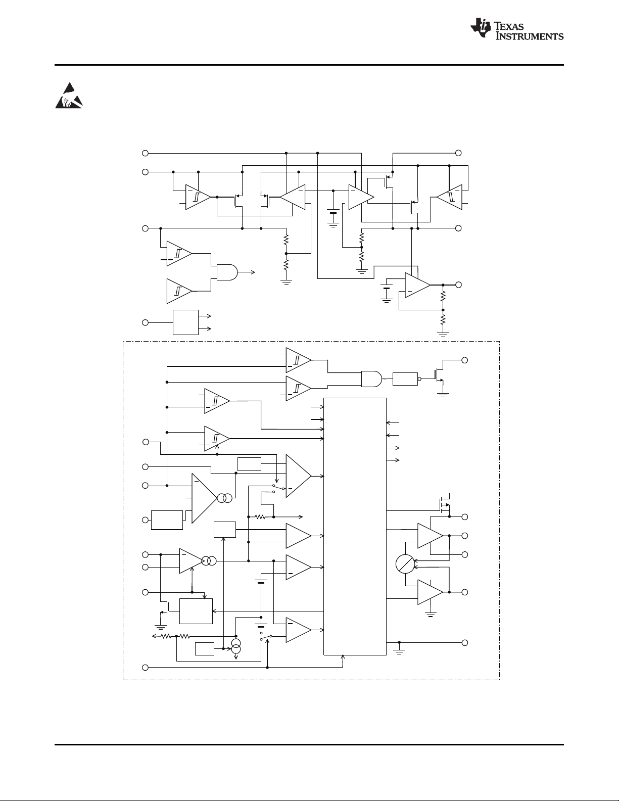
XCON
VBST1
DRVH1
SW1
DRVL1
GND
VREG5
VREG5
GND
Control
Logic
PGOOD1
GND
Delay
+
+
+
+
1V+5%/10%
1V-5%/10%
1V-30%
1V+15%
+
PWM
Skip
Ramp
Comp
+
+
VFB1
COMP1
EN1
Enable/
Soft-start
1V
+
CSN1
CSP1
TRIP
Discharge
Control
GND
100mV
+
V5SW
4.7V/4.5V
GND
VREG5
+
VREF2
GND
GND
1.25V
GND
1.25V
GND
+
VREG3
+
4.7V/4.5V
VIN
EN
+
4.2V/3.8V
150/140
Deg-C
V5OK
THOK
Ready
+
SKIPSEL1
FUNC
OSC
RF
CLK1
CLK2
Fault1
SDN1
UVP
OVP
Fault2
SDN2
Ready
GND
Channel-1Switchershown
+
VREF2
D-CAP
CUR
CLK1
VREF2
+
OCP
Ramp
Comp
+
N-OCP
100mV
OOA
Ctrl
+
VFB-AMP
CS-AMP
TPS51220
SLVS785C –OCTOBER 2007–REVISED JULY 2009
This integrated circuit can be damaged by ESD. Texas Instruments recommends that all integrated circuits be handled with
appropriate precautions. Failure to observe proper handling and installation procedures can cause damage.
ESD damage can range from subtle performance degradation to complete device failure. Precision integrated circuits may be more
susceptible to damage because very small parametric changes could cause the device not to meet its published specifications.
www.ti.com
FUNCTIONAL BLOCK DIAGRAM
Product Folder Links :TPS51220
2 Submit Documentation Feedback Copyright © 2007–2009, Texas Instruments Incorporated
TPS51220
www.ti.com
ABSOLUTE MAXIMUM RATINGS
(1)
over operating free-air temperature range (unless otherwise noted)
VIN –0.3 to 30 V
VBST1, VBST2 –0.3 to 35 V
VBST1, VBST2
SW1, SW2 –7 to 30 V
V
I
Input voltage range
(2)
CSP1, CSP2, CSN1, CSN2 –1 to 13.5 V
EN, EN1, EN2, VFB1, VFB2, TRIP, SKIPSEL1, SKIPSEL2, FUNC –0.3 to 7 V
V5SW –0.3 to 7 V
V5SW (to VREG5)
DRVH1, DRVH2 –7 to 35 V
DRVH1, DRVH2
V
O
Output voltage range
(2)
DRVL1, DRVL2, COMP1, COMP2, VREG5, RF, VREF2,
PGOOD1, PGOOD2
VREG3 –0.3 to 3.6 V
T
J
T
stg
Operating junction temperature range –40 to 125 °C
Storage temperature –55 to 150 °C
(1) Stresses beyond those listed under absolute maximum ratings may cause permanent damage to the device. These are stress ratings
only and functional operation of the device at these or any other conditions beyond those indicated under recommended operating
conditions is not implied. Exposure to absolute-maximum-rated conditions for extended periods may affect device reliability.
(2) All voltage values are with respect to the network ground terminal unless otherwise noted.
(3) Voltage values are with respect to the corresponding SW terminal.
(4) When EN is high and V5SW is grounded, or voltage is applied to V5SW when EN is low.
(3)
(4)
(3)
SLVS785C –OCTOBER 2007–REVISED JULY 2009
VALUE UNIT
–0.3 to 7 V
–7 to 7 V
–0.3 to 7 V
–0.3 to 7 V
DISSIPATION RATINGS (2 oz. Trace and Copper Pad with Solder)
PACKAGE
32 pin RHB 2.2 W 23 mW/°C 0.9 W
TA< 25°C DERATING FACTOR TA= 85°C
POWER RATING ABOVE TA= 25°C POWER RATING
RECOMMENDED OPERATING CONDITIONS
V
V
V
T
Supply
SS
voltage
I
I/O voltage V
O
Operating free-air temperature –40 85 °C
A
VIN 4.5 28 V
V5SW –0.8 6
DRVH1, DRVH2 –4.0 33
VBST1, VBST2, –0.1 33
DRVH1, DRVH2 (wrt SW1, SW2) –0.1 6
DRVH1, DRVH2 (negative overshoot -6 V for t< 20% duration of switching period) –6 33
SW1, SW2 –4.0 28
SW1, SW2 (negative overshoot -6 V for t< 20% duration of switching period) –6 28
CSP1, CSP2, CSN1, CSN2 –0.8 13
EN, EN1, EN2, VFB1, VFB2, TRIP, DRVL1, DRVL2, COMP1, COMP2, VREG5,
RF, VREF2, PGOOD1, PGOOD2, SKIPSEL1, SKIPSEL2, FUNC
VREG3 –0.1 3.5
MIN TYP MAX UNIT
–0.1 6
Copyright © 2007–2009, Texas Instruments Incorporated Submit Documentation Feedback 3
Product Folder Links :TPS51220

TPS51220
SLVS785C –OCTOBER 2007–REVISED JULY 2009
ORDERING INFORMATION
T
A
-40°C to 85°C
(1) For the most current package and ordering information, see the Package Option Addendum at the end of this document, or see the TI
website at www.ti.com.
PACKAGE
Plastic Quad Flat Pack
(32 Pin QFN)
(1)
ORDERABLE PART
NUMBER
TPS51220RHBT Tape and Reel 250
TPS51220RHBR Tape and Reel 3000
TRANSPORT MEDIA QUANTITY
www.ti.com
4 Submit Documentation Feedback Copyright © 2007–2009, Texas Instruments Incorporated
Product Folder Links :TPS51220
TPS51220
www.ti.com
ELECTRICAL CHARACTERISTICS
over operating free-air temperature range, EN = 3.3V, VIN = 12V, V5SW = 5V (unless otherwise noted)
PARAMETER TEST CONDITIONS MIN TYP MAX UNIT
SUPPLY CURRENT
I
(VINSDN)
I
(VINSTBY)
I
(VBATSTBY)
I
(V5SW)
VIN shutdown current 7 15 μA
VIN standby current 80 120 μA
V
standby current 500 μA
BAT
V5SW supply current
VREF2 OUTPUT
V
(VREF2)
VREF2 output voltage V
VREG3 OUTPUT
V
(VREG3)
I
(VREG3)
VREG3 output voltage V
VREG3 output current VREG3 = 3 V 10 15 20 mA
VREG5 OUTPUT
V
(VREG5)
I
(VREG5)
V
(THV5SW)
t
d(V5SW)
R
(V5SW)
VREG5 output voltage 6 V < VIN < 25 V
VREG5 output current mA
Switchover threshold V
Switchover delay Turning on 7.7 ms
5V SW on-resistance I
OUTPUT
V
regulation voltage
V
(VFB)
I
(VFB)
R
(Dischg)
F B
tolerance
V
input current VFBx = 1.05 V, COMPx = 1.8 V, TA= 25°C –50 50 nA
F B
CSNx discharge resistance ENx = 0 V, CSNx = 0.5 V, TA= 25°C 20 40 Ω
VOLTAGE TRANSCONDUCTANCE AMPLIFIER
Gmv Gain TA= 25°C 500 μS
V
ID
I
(COMPSINK)
I
(COMPSRC)
Differential input voltage
range
COMP maximum sink
current
COMP maximum source
current
(1) Specified by design. Detail external condition follows application circuit of Figure 53.
VIN shutdown current, TA= 25°C,
No Load, EN = 0V, V5SW = 0 V
VIN standby current, TA= 25°C, No Load,
EN1 = EN2 = V5SW = 0 V
V
standby current, TA= 25°C, No Load
BAT
SKIPSEL2 = 2V, EN2 = open, EN1 = V5SW = 0V
V5SW current, TA= 25°C, No Load,
ENx = 5V, VFBx = 1.05 V
I
< ±10 μA, TA= 25°C 1.98 2.00 2.02
(VREF2)
I
< ±100 μA, 4.5V < VIN < 25 V 1.97 2.00 2.03
(VREF2)
V5SW = 0 V, I
V5SW = 0 V, 0 mA < I
5.5 V < VIN < 25 V
V5SW = 0 V, I
V5SW = 0 V, 0 mA < I
V5SW = 0 V, 0 mA < I
5.5 V < VIN < 25 V
= 0 mA, TA= 25°C 3.279 3.313 3.347
(VREG3)
< 10 mA,
(VREG3)
= 0 mA, TA= 25°C 4.99 5.04 5.09
(VREG5)
< 100 mA,
(VREG5)
< 100 mA,
(VREG5)
TRIP = 5 V 1.2 mA
TRIP = 0 V 1.4 mA
V5SW = 0 V, VREG5 = 4.5 V 100 150 200
V5SW = 5 V, VREG5 = 4.5 V 200 300 400
Turning on 4.55 4.7 4.8
Hysteresis 0.15 0.20 0.25
= 100 mA 0.5 Ω
(VREG5)
TA= 25°C, No Load 0.9925 1.000 1.0075
TA= –40°C to 85°C , No Load 0.990 1.000 1.010
COMPx = 1.8 V 33 μA
COMPx = 1.8 V –33 μA
SLVS785C –OCTOBER 2007–REVISED JULY 2009
(1)
3.135 3.300 3.400
4.90 5.03 5.15
4.50 5.03 5.15 V
–30 30 mV
V
V
Copyright © 2007–2009, Texas Instruments Incorporated Submit Documentation Feedback 5
Product Folder Links :TPS51220
TPS51220
SLVS785C –OCTOBER 2007–REVISED JULY 2009
ELECTRICAL CHARACTERISTICS (continued)
over operating free-air temperature range, EN = 3.3V, VIN = 12V, V5SW = 5V (unless otherwise noted)
PARAMETER TEST CONDITIONS MIN TYP MAX UNIT
CURRENT AMPLIFIER
G
C
V
IC
V
ID
Gain
Common mode input
voltage range
Differential input voltage
range
POWERGOOD
V
(THPG)
I
(PG)
t
(PGDLY)
PG threshold PG in from higher 102.5% 105% 107.5%
PG sink current PGOOD = 0.5 V 5 mA
PGOOD delay Delay for PG in 0.8 1 1.2 ms
SOFTSTART
t
(SSDYL)
t
(SS)
Soft-start delay time Delay for Soft Start, ENx = Hi to SS-ramp starts 200 μs
Soft-start Time Internal Soft Start 960 μs
FREQUENCY AND DUTY CONTROL
f
(SW)
V
(THRF)
f
(SYNC)
Switching frequency Rf = 330 kΩ 273 303 333 kHz
RF threshold
Syncronization Input
Frequency Range
(2)
tONmin Minimum On Time V
t
min Minimum Off Time V
OFF
t
V
V
D
(DTH)
(DTL)
Dead time
DRVH-off threshold DRVH to GND
DRVL-off threshold DRVL to GND
OUTPUT DRIVERS
R
(DRVH)
R
(DRVL)
DRVH resistance Ω
DRVL resistance Ω
CURRENT SENSE
V
(OCL-ULV)
V
(OCL-LV)
V
(ZC)
Current limit threshold
(ultra-low voltage)
Current limit threshold
(low voltage)
Zero cross detection
comparator Offset
Negative current limit TRIP = 0V/2V, TA= 25°C –24 –31 –38
V
(OCLN-ULV)
threshold
(ultra-low voltage)
Negative current limit TRIP = 3.3V/5V, TA= 25°C –51 –60 –69
V
(OCLN-LV)
threshold
(low voltage)
(2) Specified by design.
TRIP = 0V/2V, CSN = 5V, TA= 25°C
TRIP = 3.3V/5V, CSN = 5V, TA= 25°C
TA= 25°C –75 75 mV
PG in from lower 92.5% 95% 97.5%
PG hysteresis 5%
Lo to Hi 0.7 1.3 2 V
Hysteresis 0.2 V
= 90% to 10%, No Load 120 150 ns
(DRVH)
= 10% to 90%, No Load 290 440 ns
(DRVH)
DRVH-off to DRVL-on 10 30 50 ns
DRVL-off to DRVH-on 30 40 70 ns
(2)
(2)
Source, V
Sink, V
(DRVH-SW)
Source, V
Sink, V
(DRVL-GND)
(VBST-DRVH)
(VREG5-DRVL)
= 0.1 V 1.7 5
= 0.1 V 1 3
= 0.1 V 1.3 4
= 0.1 V 0.7 2
TRIP = 0V/2V, TA= 25°C 27 31 35
TRIP = 0V/2V 25 31 37
TRIP = 3.3V/5V, TA= 25°C 56 60 64
TRIP = 3.3V/5V 54 60 66
0.95V < CSNx < 12.6V –4 0 4 mV
TRIP = 0V/2V –22 –31 –40
TRIP = 3.3V/5V –49 –60 –71
(2)
(2)
0 13 V
200 1000 kHz
www.ti.com
3.333
1.667
1 V
1 V
mV
mV
6 Submit Documentation Feedback Copyright © 2007–2009, Texas Instruments Incorporated
Product Folder Links :TPS51220
www.ti.com
SLVS785C –OCTOBER 2007–REVISED JULY 2009
ELECTRICAL CHARACTERISTICS (continued)
over operating free-air temperature range, EN = 3.3V, VIN = 12V, V5SW = 5V (unless otherwise noted)
PARAMETER TEST CONDITIONS MIN TYP MAX UNIT
UVP, OVP AND UVLO
V
(OVP)
t
(OVPDLY)
V
(UVP)
t
(UVPDLY)
V
(UVREF2)
V
(UVREG3)
V
(UVREG5)
INTERFACE AND LOGIC THRESHOLD
V
(EN)
V
(EN12)
V
(EN12SS)
V
(EN12SSEND)
I
(EN12)
V
(SKIPSEL)
V
(TRIP)
V
(FUNC)
I
(TRIP)
I
(SKIPSEL)
BOOT STRAP SW
V
(FBST)
I
(BSTLK)
THERMAL SHUTDOWN
T
(SDN)
OVP Trip Threshold OVP detect 110% 115% 120%
OVP Prop Delay 1.5 μs
UVP Trip Threshold UVP detect 65% 70% 73%
UVP Delay 0.8 1 1.2 ms
VREF2 UVLO Threshold
VREG3 UVLO Threshold V
VREG5 UVLO Threshold
EN Threshold V
EN1/EN2 Threshold V
EN1/EN2 SS Start
Threshold
EN1/EN2 SS End
Threshold
Wake up 1.7 1.8 1.9 V
Hysteresis 75 100 125 mV
Wake up 3 3.1 3.2
Hysteresis 0.10 0.15 0.20
Wake up 4.1 4.2 4.3 V
Hysteresis 0.35 0.40 0.44 V
Wake up 0.8 1 1.2
Hysteresis 0.1 0.2 0.3
Wake up 0.45 0.50 0.55
Hysteresis 0.1 0.2 0.3
SS-ramp start threshold at external soft start 1 V
SS-End threshold at external soft start
(3)
EN1/EN2 Source Current VEN1/EN2 = 0V 1.5 2 2.6 μA
Continuous 1.5
SKIPSEL1/SKIPSEL2
Setting Voltage
Auto Skip 1.9 2.1
OOA Skip (min 1/8 Fsw) 3.2 3.4
OOA Skip (min 1/16 Fsw) 3.8
V
(OCL-ULV)
V
TRIP Setting Voltage V
(OCL-ULV)
V
(OCL-LV)
V
(OCL-LV)
, Discharge ON 1.5
, Discharge OFF 1.9 2.1
, Discharge OFF 3.2 3.4
, Discharge ON 3.8
Current mode, OVP enable 1.5
FUNC Setting Voltage V
D-CAP mode, OVP disable 1.9 2.1
D-CAP mode, OVP enable 3.2 3.4
Current mode, OVP disable 3.8
TRIP Input Current μA
SKIPSEL Input Current μA
Forward Voltage V
TRIP = 0 V –1 1
TRIP =5 V –1 1
SKIPSELx = 0 V –0.5 0.5
SKIPSELx = 5 V –0.5 0.5
VREG5-VBST
, IF= 10 mA, TA= 25°C 0.10 0.20 V
VBST Leakage Current VBST = 30 V, SW = 25 V 0.01 1.5 μA
Thermal SDN Threshold °C
Shutdown temperature
Hysteresis
(3)
(3)
TPS51220
2 V
V
150
10
(3) Specified by design.
Copyright © 2007–2009, Texas Instruments Incorporated Submit Documentation Feedback 7
Product Folder Links :TPS51220
DRVH2
VIN
VREG3
EN2
DRVH1
V5SW
RF
EN1
PGOOD2
SKIPSEL2
CSP2
CSN2
PGOOD1
SKIPSEL1
CSP1
CSN1
VFB1
SW1
VBST1
DRVL1
VREG5
GND
DRVL2
VBST2
SW2
COMP1
FUNC
EN
VREF2
TRIP
COMP2
VFB2
24
23
22
21
20
19
18
17
1
2
3
4
5
6
7
8
9
10
11
12
13
14
15
16
32
31
30
29
28
27
26
25
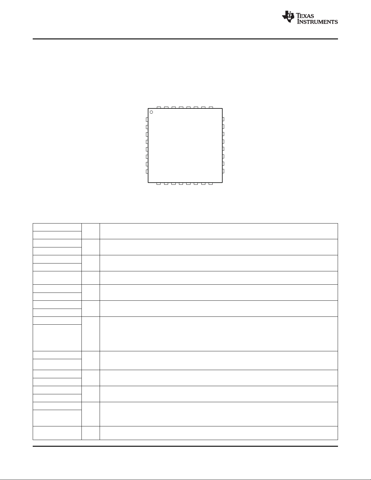
RHBPACKAGE
(TOP VIEW)
TPS51220
SLVS785C –OCTOBER 2007–REVISED JULY 2009
PINOUT
www.ti.com
DEVICE INFORMATION
TERMINAL FUNCTIONS
TERMINAL
NAME NO.
DRVH1 1
DRVH2 24
SW2 25
SW1 32
VREG3 22 O
EN1 4
EN2 21
PGOOD1 5
PGOOD2 20
SKIPSEL1 6 Skip mode selection pin.
SKIPSEL2 19
CSP1 7 Current sense comparator inputs (+). An RC network with high quality X5R or X7R ceramic capacitor should
CSP2 18
CSN1 8
CSN2 17
VFB1 9
VFB2 16
COMP1 10 Loop compensation pin for current mode (error amplifier output). Connect R (and C if required) from this pin
COMP2 15
RF 3 I/O
8 Submit Documentation Feedback Copyright © 2007–2009, Texas Instruments Incorporated
I/O DESCRIPTION
High-side MOSFET gate driver outputs. Source 1.7Ω, sink 1.0Ω, SW-node referenced floating driver. Drive
O
voltage corresponds to VBST to SW voltage.
I/O High-side MOSFET gate driver returns.
Always alive 3.3-V, 10-mA low dropout linear regulator output. Bypass to (signal) GND with more than 1-μF
ceramic capacitor. Runs from VIN supply or from VREG5 when it is switched over to V5SW input.
Channel 1 and channel 2 SMPS enable Pins. When turning on, apply greater than 0.55 V and less than 6 V,
I
or be floating. Connect to GND to disable. Adjustable soft-start capacitance to be attached here.
Power Good window comparator outputs for channel 1 and channel 2. The applied voltage should be less
O
than 6 V, and the recommended pull-up resistance value is from 100 kΩ to 1 MΩ.
I
I/O be used to extract voltage drop across DCR. 0.1 μF is a good value to start the design. See the current
I
I
I
GND: Continuous conduction mode
VREF2: Auto skip
VREG3: OOA auto skip, maximum 7 skips (suitable for fsw< 400 kHz)
VREG5: OOA auto skip, maximum 15 skips (suitable for equal to or greater than 400 kHz)
sensing scheme section for more details.
Current sense comparator inputs (–). See the current sensing scheme section. Used as power supply for the
current sense circuit for 5 V or higher output voltage setting. Also, used for output discharge terminal.
SMPS voltage feedback inputs. Connect the feedback resistors divider, and should be referred to (signal)
GND.
to VREF2 for proper loop compensation with current mode operation. Ramp compensation adjustable pin for
D-CAP mode, connect R from this pin to VREF2. 10 kΩ is a good value to start the design. 6 kΩ to 20 kΩ
can be chosen. See the D-CAP MODE section for more details.
Frequency setting pin. Connect a frequency setting resistor to (signal) GND. Connect to an external clock for
synchronization.
Product Folder Links :TPS51220

TPS51220
www.ti.com
TERMINAL FUNCTIONS (continued)
TERMINAL
NAME NO.
FUNC 11 I
VREF2 13 O 2-V Reference Output. Bypass to (signal) GND by 0.22μF ceramic capacitor.
TRIP 14 I
EN 12 I
VBST1 31 Supply inputs for high-side NFET driver (boot strap Terminal). Connect a capacitor (0.1μF or greater is
VBST2 26
DRVL1 30
DRVL2 27
V5SW 2 I voltage is higher than 4.8 V, switch-over function will be enabled. (Note) When switch-over is enabled,
VREG5 29 O
VIN 23 I Supply input for 5-V and 3.3-V linear regulator. Typically connected to VBAT.
GND 28 – Ground.
I/O DESCRIPTION
Control architecture and OVP function selection pin.
GND: Current mode, OVP enable
VREF2: D-CAP mode, OVP disable
VREG3: D-CAP mode, OVP enable
VREG5: Current mode, OVP disable
Overcurrent trip level and discharge mode selection pin.
GND: V
(OCL-ULV)
VREF2: V
VREG3: V
VREG5: V
(OCL-ULV)
(OCL-LV)
(OCL-LV)
, Discharge on
, Discharge off
, Discharge off
, Discharge on
VREF2 and VREG5 Linear Regulators Enable Pin. When turning on, apply greater than 1.2V and less than
6V. Connect to GND to Disable.
I recommended) from this pin to respective SW terminal. Additional SB diode from VREG5 to this pin is an
optional.
O Low-side MOSFET gate driver outputs. Source 1.3 Ω, sink 0.7 Ω, GND referenced driver.
VREG5 switchover power supply input pin. When EN1 is high, PGOOD1 indicates GOOD and V5SW
VREG5 output voltage will be almost the same as V5SW input voltage.
5-V, 100-mA low-dropout linear regulator output. Bypass to (power) GND using a 10-μF ceramic capacitor.
Runs from VIN supply. Internally connected to VBST and DRVL. Shuts off with EN. Switches over to V5SW
when 4.8 V or above is provided. (Note: when switch-over (above V5SW) is enabled, VREG5 output voltage
is approximately the same as V5SW input voltage.)
SLVS785C –OCTOBER 2007–REVISED JULY 2009
Copyright © 2007–2009, Texas Instruments Incorporated Submit Documentation Feedback 9
Product Folder Links :TPS51220
0
20
40
60
80
100
120
-50 0 50 100 150
T -JunctionTemperature- CJ°
I -StandbyCurrent- Am
(VINSTBY)
0
20
40
60
80
100
120
5 10 15 20 25 30
V -VINInputVoltage-V
I
I -StandbyCurrent- mA
(VINSTBY)
0
3
6
9
12
15
5 10 15 20 25 30
V -VINInputVoltage-V
I
RT
I -ShutdownCurrent- μA
(VINSDN)
0
3
6
9
12
15
-50 0 50 100 150
T -JunctionTemperature- CJ°
I -ShutdownCurrent- μA
(VINSDN)
VIN=12V
TPS51220
SLVS785C –OCTOBER 2007–REVISED JULY 2009
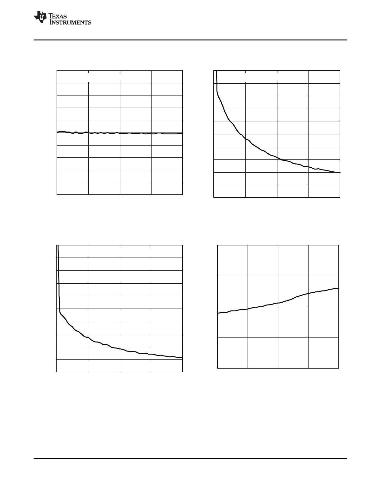
VIN SHUTDOWN CURRENT VIN SHUTDOWN CURRENT
vs vs
INPUT VOLTAGE JUNCTION TEMPERATURE
www.ti.com
TYPICAL CHARACTERISTICS
Figure 2. Figure 3.
VIN STANDBY CURRENT VIN STANDBY CURRENT
JUNCTION TEMPERATURE INPUT VOLTAGE
vs vs
Figure 4. Figure 5.
10 Submit Documentation Feedback Copyright © 2007–2009, Texas Instruments Incorporated
Product Folder Links :TPS51220
0.0
0.1
0.2
0.3
0.4
0.5
0.6
0.7
0.8
0.9
1.0
5 10 15 20 25
V - VIN Input Voltage - V
I
I -BatteryCurrent-mA
(VBAT)
EN=on,EN1=on,EN2=off
1.98
1.99
2.00
2.01
2.02
-100 -50 0 50 100
I -OutputCurrent- μA
O(VREF2)
V -OutputVoltage-V
O(VREF2)
VIN=12V
0.0
0.1
0.2
0.3
0.4
0.5
0.6
0.7
0.8
0.9
1.0
5 10 15 20 25
V - VIN Input Voltage - V
I
I -BatteryCurrent-mA
(VBAT)
EN=on,EN1=on,EN2=on
0.0
0.1
0.2
0.3
0.4
0.5
0.6
0.7
0.8
0.9
1.0
5 10 15 20 25
V -VINInputVoltage-V
I
I -BatteryCurrent-mA
(VBAT)
EN=on,EN1=off,EN2=on
www.ti.com
TPS51220
SLVS785C –OCTOBER 2007–REVISED JULY 2009
NO LOAD BATTERY CURRENT NO LOAD BATTERY CURRENT
BATTERY CURRENT VREF2 OUTPUT VOLTAGE
vs vs
INPUT VOLTAGE INPUT VOLTAGE
Figure 6. Figure 7.
vs vs
INPUT VOLTAGE OUTPUT CURRENT
TYPICAL CHARACTERISTICS (continued)
Copyright © 2007–2009, Texas Instruments Incorporated Submit Documentation Feedback 11
Figure 8. Figure 9.
Product Folder Links :TPS51220
270
280
290
300
310
320
330
-50 0 50 100 150
T -JunctionTemperature- CJ°
f -SwitchingFrequency-kHz
(SW)
RF=330kΩ
0.00
0.05
0.10
0.15
0.20
0.25
-50 0 50 100 150
T -JunctionTemperature- CJ°
V -ForwardVoltage-V
(FBST)
3.20
3.25
3.30
3.35
3.40
0 2 4 6 8 10
I -OutputCurrent-mA
O(VREG3)
V -OutputVoltage-V
O(VREG3)
VIN=12V
4.90
4.95
5.00
5.05
5.10
0 20 40 60 80 100
I -OutputCurrent-mA
O(VREG5)
V -OutputVoltage-V
O(VREG5)
VIN=12V
TPS51220
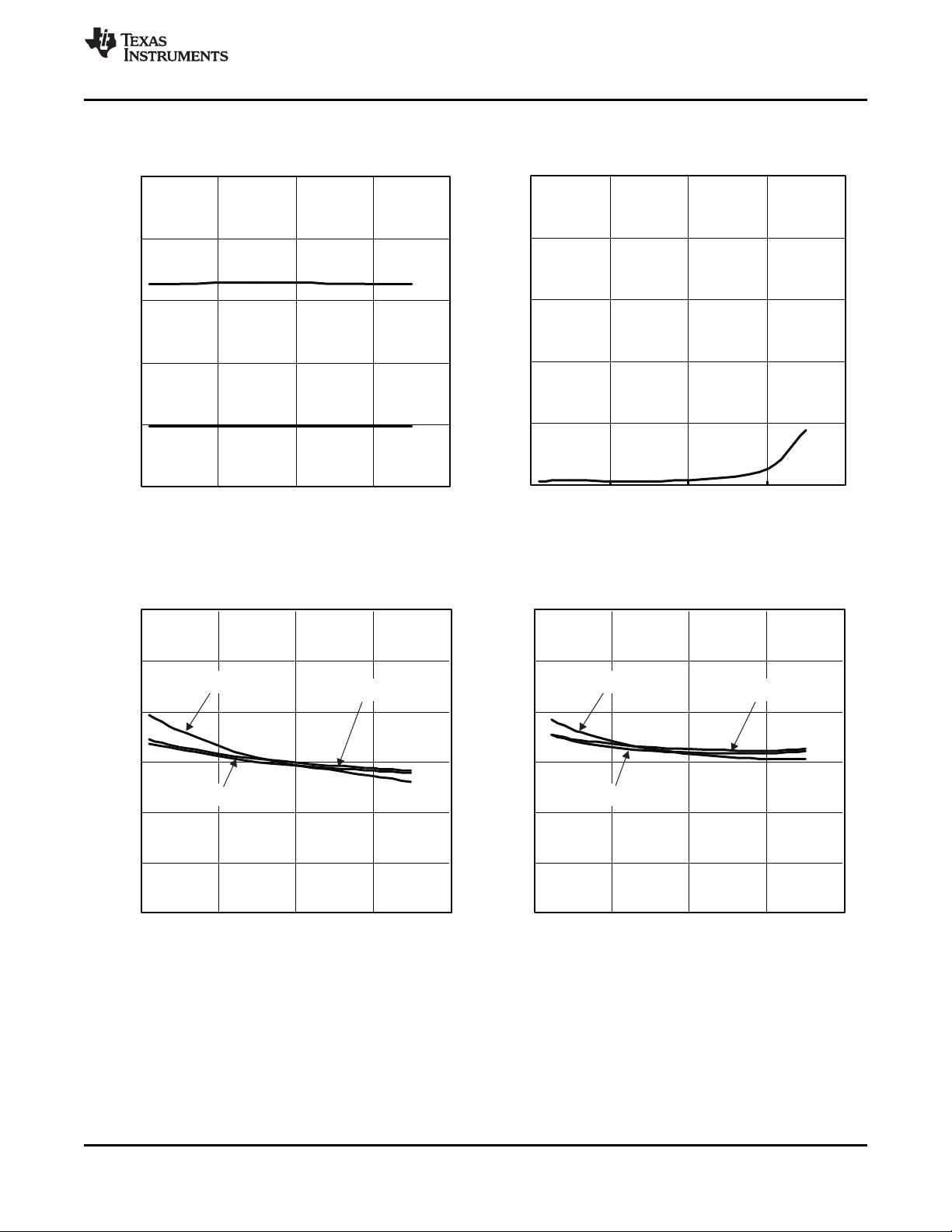
SLVS785C –OCTOBER 2007–REVISED JULY 2009
www.ti.com
VREG3 OUTPUT VOLTAGE VREG5 OUTPUT VOLTAGE
OUTPUT CURRENT OUTPUT CURRENT
SWITCHING FREQUENCY FORWARD VOLTAGE OF BOOST SW
JUNCTION TEMPERATURE JUNCTION TEMPERATURE
vs vs
Figure 10. Figure 11.
vs vs
TYPICAL CHARACTERISTICS (continued)
12 Submit Documentation Feedback Copyright © 2007–2009, Texas Instruments Incorporated
Figure 12. Figure 13.
Product Folder Links :TPS51220
T -JunctionTemperature- CJ°
25
27
29
31
33
35
37
V -CurrentLimitThreshold-mV
(OCL-ULV)
-50 0 50 100 150
CSN=1V
CSN=5V
CSN=12V
T -JunctionTemperature- CJ°
54
56
58
60
62
64
66
V -CurrentLimitThreshold-mV
(OCL-LV)
-50 0 50 100 150
CSN=1V
CSN=5V
CSN=12V
50
70
90
110
130
150
-50 0 50 100 150
T -JunctionTemperature- CJ°
OVP/UVP Threshold-%
OVP
UVP
0.0
0.3
0.6
0.9
1.2
1.5
-50 0 50 100 150
T -JunctionTemperature- CJ°
I -VBSTLeakageCurrent- μA
lkg
www.ti.com
TPS51220
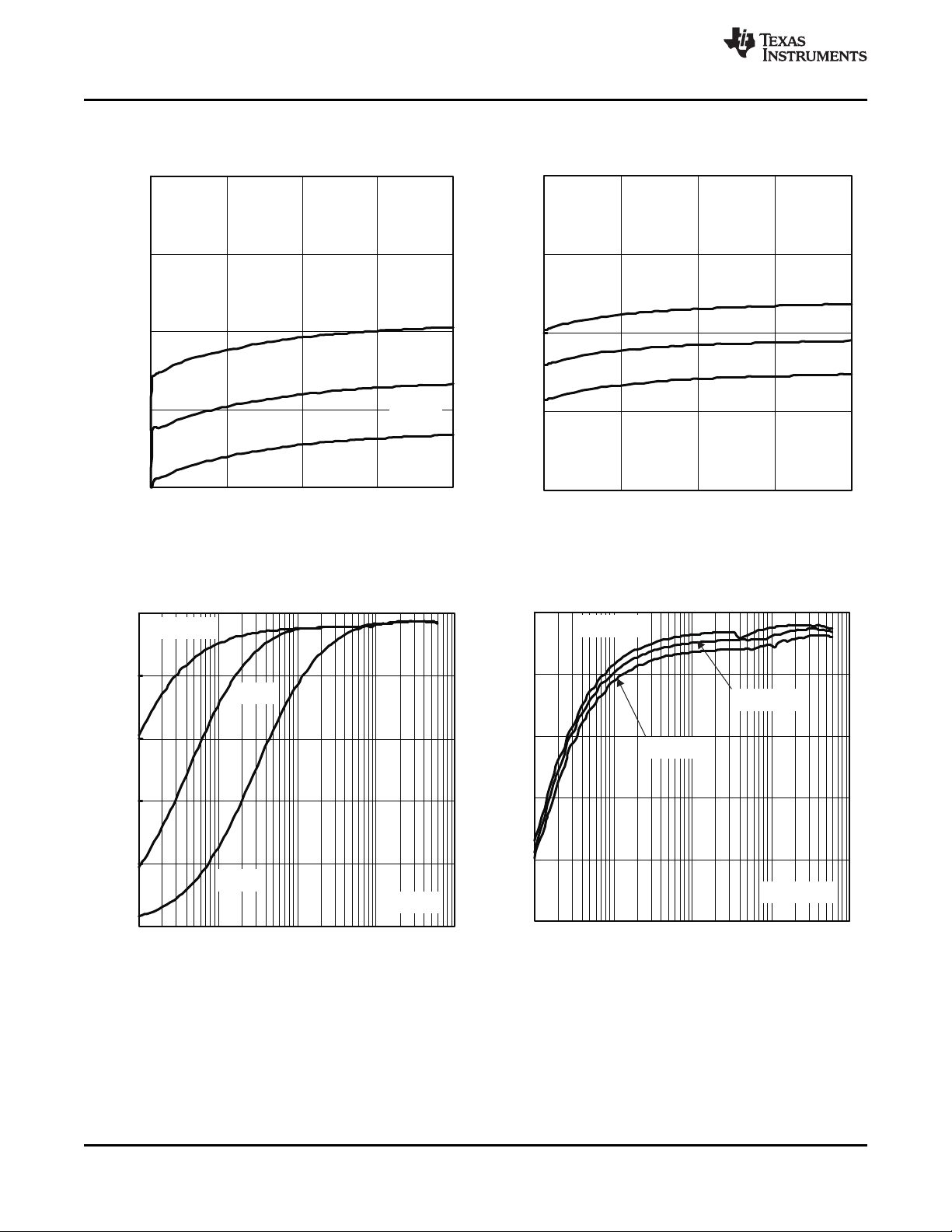
SLVS785C –OCTOBER 2007–REVISED JULY 2009
OVP/UVP THRESHOLD VOLTAGE VBST LEAKAGE CURRENT
JUNCTION TEMPERATURE JUNCTION TEMPERATURE
CURRENT LIMIT THRESHOLD CURRENT LIMIT THRESHOLD
JUNCTION TEMPERATURE JUNCTION TEMPERATURE
vs vs
Figure 14. Figure 15.
vs vs
TYPICAL CHARACTERISTICS (continued)
Copyright © 2007–2009, Texas Instruments Incorporated Submit Documentation Feedback 13
Figure 16. Figure 17.
Product Folder Links :TPS51220
0
20
40
60
80
100
0.001 0.01 0.1 1 10
I -5-VOutputCurrent- A
O1
h
-Efficiency-%
Auto-skip
CCM
VIN=12V
OOA
50
60
70
80
90
100
0.001 0.01 0.1 1 10
I -5-VOutputCurrent- A
O1
h
-Efficiency-%
Auto-skip
VIN=7V
VIN=12V
VIN=21V
3.20
3.25
3.30
3.35
3.40
5 10 15 20 25
V -VINInputVoltage-V
I
V -3.3-VOutputVoltage-V
O2
IO=0A
IO=6A
IO=3A
CCM
4.90
4.95
5.00
5.05
5.10
5 10 15 20 25
V -VINInputVoltage-V
I
V -5-VOutputVoltage-V
O1
IO=0A
IO=6A
IO=3A
CCM
TPS51220
SLVS785C –OCTOBER 2007–REVISED JULY 2009
www.ti.com
5-V OUTPUT VOLTAGE 3.3-V OUTPUT VOLTAGE
OUTPUT CURRENT OUTPUT CURRENT
vs vs
INPUT VOLTAGE INPUT VOLTAGE
Figure 18. Figure 19.
5-V EFFICIENCY 5-V EFFICIENCY
vs vs
TYPICAL CHARACTERISTICS (continued)
14 Submit Documentation Feedback Copyright © 2007–2009, Texas Instruments Incorporated
Figure 20. Figure 21.
Product Folder Links :TPS51220

0
50
100
150
200
250
300
350
400
0 0.5 1 1.5 2
I -5-VOutputCurrent- A
O1
f -SwithchingFrequency-kHz
(SW)
VIN=12V
Auto-skip
CCM
OOA
0
50
100
150
200
250
300
350
400
0 0.5 1 1.5 2
I -3.3-VOutputCurrent- A
O2
f -SwithchingFrequency-kHz
(SW)
VIN=12V
Auto-skip
CCM
OOA
0
20
40
60
80
100
0.001 0.01 0.1 1 10
I -3.3-VOutputCurrent- A
O2
h
-Efficiency-%
Auto-skip
CCM
VIN=12V
5-VSwitcherON
(Auto-skip)
OOA
40
50
60
70
80
90
100
0.001 0.01 0.1 1 10
I -3.3-VOutputCurrent- A
O2
h
-Efficiency-%
Auto-skip
VIN=7V
VIN=12V
VIN=21V
5-VSwitcherON
(Auto-skip)
www.ti.com
TPS51220
SLVS785C –OCTOBER 2007–REVISED JULY 2009
3.3-V EFFICIENCY 3.3-V EFFICIENCY
TYPICAL CHARACTERISTICS (continued)
OUTPUT CURRENT OUTPUT CURRENT
5-V SWITCHING FREQUENCY 3.3-V SWITCHING FREQUENCY
OUTPUT CURRENT OUTPUT CURRENT
vs vs
Figure 22. Figure 23.
vs vs
Copyright © 2007–2009, Texas Instruments Incorporated Submit Documentation Feedback 15
Figure 24. Figure 25.
Product Folder Links :TPS51220

4.90
4.95
5.00
5.05
5.10
0 1 2 3 4 5 6
I -5-VOutputCurrent- A
O1
V -5-VOutputVoltage-V
O1
CCM
Auto-skip
OOA
D-CAP mode
Cout-ESR=40mW
Rgv=10k
VIN=12V
3.20
3.25
3.30
3.35
3.40
0 1 2 3 4 5 6
I -3.3-VOutputCurrent- A
O2
V -3.3-VOutputVoltage-V
O2
CCM
Auto-skip
OOA
D-CAP mode
Cout-ESR=18m
Rgv=10k
VIN=12V
W
4.90
4.95
5.00
5.05
5.10
0 1 2 3 4 5 6
I -5-VOutputCurrent- A
O1
V -5-VOutputVoltage-V
O1
CCM
Auto-skip
OOA
CurrentMode
Rgv=10k
VIN=12V
3.20
3.25
3.30
3.35
3.40
0 1 2 3 4 5 6
I -3.3-VOutputCurrent- A
O2
V -3.3-VOutputVoltage-V
O2
CCM
Auto-skip
OOA
CurrentMode
Rgv=10k
VIN=12V
TPS51220
SLVS785C –OCTOBER 2007–REVISED JULY 2009
www.ti.com
5-V OUTPUT VOLTAGE 3.3-V OUTPUT VOLTAGE
OUTPUT CURRENT OUTPUT CURRENT
5-V OUTPUT VOLTAGE 3.3-V OUTPUT VOLTAGE
OUTPUT CURRENT OUTPUT CURRENT
vs vs
Figure 26. Figure 27.
vs vs
TYPICAL CHARACTERISTICS (continued)
Figure 28. Figure 29.
16 Submit Documentation Feedback Copyright © 2007–2009, Texas Instruments Incorporated
Product Folder Links :TPS51220

t-Time-1ms/div
EN2(5V/div)
VO2(5V/div)
PGOOD2(5V/div)
DRVL2(5V/div)
t-Time-1ms/div
EN1(5V/div)
VO1(5V/div)
PGOOD1(5V/div)
DRVL1(5V/div)
t-Time-1ms/div
EN2(5V/div)
VO2(2V/div)
PGOOD2(5V/div)
VIN=12V
Iout=6A
t-Time-1ms/div
EN1(5V/div)
VO1(2V/div)
PGOOD1(5V/div)
VIN=12V
Iout=6A
www.ti.com
TPS51220
SLVS785C –OCTOBER 2007–REVISED JULY 2009
5.0-V START-UP WAVEFORMS 3.3-V START-UP WAVEFORMS
TYPICAL CHARACTERISTICS (continued)
Figure 30. Figure 31.
5.0-V SOFT-STOP WAVEFORMS 3.3-V SOFT-STOP WAVEFORMS
Copyright © 2007–2009, Texas Instruments Incorporated Submit Documentation Feedback 17
Figure 32. Figure 33.
Product Folder Links :TPS51220

-80
-60
-40
-20
0
20
40
60
80
100 1K 10K 100K 1M
f-Frequency-kHz
Gain-dB
-180
-135
-90
-45
0
45
90
135
180
Phase-°
Gain
Phase
VIN=12V
Currentmode
-80
-60
-40
-20
0
20
40
60
80
100 1K 10K 100K 1M
f-Frequency-kHz
Gain-dB
-180
-135
-90
-45
0
45
90
135
180
Phase-°
VIN=12V
CurrentMode
Phase
Gain
t-Time-100 ms/div
I
IND
(5A/div)
VO1(100mV/div)
IO1(5A/div)
VIN=12V, Auto-skip
t-Time-100 ms/div
I
IND
(5A/div)
VO2(100mV/div)
IO2(5A/div)
VIN=12V, Auto-skip
TPS51220
SLVS785C –OCTOBER 2007–REVISED JULY 2009
www.ti.com
5.0-V LOAD TRANSIENT RESPONSE 3.3-V LOAD TRANSIENT RESPONSE
TYPICAL CHARACTERISTICS (continued)
Figure 34. Figure 35.
5.0-V BODE-PLOT – GAIN AND PHASE 3.3-V BODE-PLOT – GAIN AND PHASE
vs vs
FREQUENCY FREQUENCY
18 Submit Documentation Feedback Copyright © 2007–2009, Texas Instruments Incorporated
Figure 36. Figure 37.
Product Folder Links :TPS51220

t-Time-2ms/div
VREG5(100mV/div)
VO1(100mV/div)
www.ti.com
TPS51220
SLVS785C –OCTOBER 2007–REVISED JULY 2009
TYPICAL CHARACTERISTICS (continued)
5.0-V SWITCH-OVER WAVEFORMS
Figure 38.
Copyright © 2007–2009, Texas Instruments Incorporated Submit Documentation Feedback 19
Product Folder Links :TPS51220

200ms
960ms
Vout1
EN1
EN1
Vout1
External
Soft-start
time
EN1>1V
EN1<2V
1)Internal
Soft-start
2)External
Soft-start
TPS51220
SLVS785C –OCTOBER 2007–REVISED JULY 2009
DETAILED DESCRIPTION
ENABLE AND SOFT START
When EN is Low, the TPS51220 is in the shutdown state. The 3.3-V LDO only stays alive, and consumes 7 μA
(typically). When EN becomes High, the TPS51220 is in the standby state. The 2-V reference and the 5-V LDO
become enabled, and consume approximately 80 μA with no load condition, and are ready to turn on SMPS
channels. Each SMPS channel is turned on when ENx becomes High. After ENx is set to high, the TPS51220
begins softstart, and ramps up the output voltage from zero to the target voltage with 0.96 ms. However, if a
slower soft-start is required, an external capacitor can be tied from the ENx pin to GND. In this case, the
TPS51220 charges the external capacitor with the integrated 2-μA current source. An approximate external softstart time would be t
capacitance is more than 2.2nF.
EX-SS
= CEX/ I
, which means the time from ENx = 1V to ENx = 2V. The recommend
EN12
www.ti.com
Figure 39. Enable and Soft-start Timing
Table 1. Enable Logic States
EN EN1 EN2 VREG3 VREF2 VREG5 CH1 CH2
GND Don’t Care Don’t Care ON Off Off Off Off
Hi Lo Lo ON ON ON Off Off
Hi Hi Lo ON ON ON ON Off
Hi Lo Hi ON ON ON Off ON
Hi Hi Hi ON ON ON ON ON
Pre-Biased Startup
The TPS51220 supports a pre-biased start up by preventing negative inductor current during soft-start in the
condition the output capacitor has some charge. The initial DRVH signal waits until the voltage feedback signal
becomes greater than the internal reference ramping up by soft-start function. After that, the start-up manner is
the same as the way of fully discharged soft start condition. This manner is regardless of the SKIPSELx
selection.
20 Submit Documentation Feedback Copyright © 2007–2009, Texas Instruments Incorporated
Product Folder Links :TPS51220

TPS51220
www.ti.com
3.3V, 10mA LDO (VREG3)
A 3.3-V, 10mA, linear regulator is integrated in the TPS51220. This LDO services some of the analog supply rail
for the device and provides a handy standby supply for 3.3-V Always On voltage in the notebook system. Apply a
2.2-μF (at least 1-μF), high quality X5R or X7R ceramic capacitor from VREG3 to (signal) GND in adjacent to the
device.
2V, 100μA Sink/ Source Reference (VREF2)
This voltage is used for the reference of the loop compensation network. Apply a 0.22-μF (at least 0.1-μF), high
quality X5R or X7R ceramic capacitor from VREF2 to (signal) GND in adjacent to the device.
5.0V, 100mA LDO (VREG5)
A 5.0-V, 100mA, linear regulator is integrated in the TPS51220. This LDO services the main analog supply rail
for the device and provides the current for gate drivers until switch-over function becomes enable. Apply a 10-μF
(at least 4.7-μF), high quality X5R or X7R ceramic capacitor from VREG5 to (power) GND in adjacent to the
device.
VREG5 SWITCHOVER
When EN1 is high, PGOOD1 indicates GOOD and more than 4.7 V is applied to V5SW, the internal 5-V LDO is
shut off and the VREG5 is shorted to V5SW by an internal MOSFET after a 7.7-ms delay. When the V5SW
voltage becomes lower than 4.5 V, EN1 becomes low, or PGOOD1 indicates BAD, the internal switch is turned
off and the internal 5-V LDO resumes immediately
SLVS785C –OCTOBER 2007–REVISED JULY 2009
BASIC PWM OPERATIONS
The main control loop of the SMPS is designed as a fixed frequency, pulse width modulation (PWM) controller. It
supports two control schemes; a peak current mode and a proprietary D-CAP mode. Current mode achieves
stable operation in any type of capacitors including low ESR capacitor(s) such as ceramic or specialty polymer
capacitors. D-CAP mode does not require an external compensation circuit, and is suitable for relatively larger
ESR capacitor(s) configuration. These control schemes are selected with FUNC-pin; see Table 4.
CURRENT MODE
The current mode scheme uses the output voltage information and the inductor current information to regulate
the output voltage. The output voltage information is sensed by VFBx pin. The signal is compared with the
internal 1V reference and the voltage difference is amplified by a transconductance amplifier (VFB-AMP). The
inductor current information is sensed by CSPx and CSNx pins. The voltage difference is amplified by another
transconductance amplifier (CS-AMP). The output of the VFB-AMP indicates the target peak inductor current. If
the output voltage goes down, the TPS51220 increases the target inductor current to raise the output voltage, on
the other hand, if the output voltage goes up the TPS51220 decreases the target inductor current to reduce the
output voltage.
At the beginning of each clock cycle, the high-side MOSFET is turned on, or becomes ‘ON’ state. The high-side
MOSFET is turned off, or becomes OFF state, after the inductor current becomes the target value which is
determined by the combination value of the output of the VFB-AMP and a ramp compensation signal. The ramp
compensation signal is used to prevent sub-harmonic oscillation of the inductor current control loop. The highside MOSFET is turned on again at the next clock cycle. By repeating the operation in this manner, the controller
regulates the output voltage. The synchronous low-side or the rectifying MOSFET is turned on each OFF state to
keep the conduction loss minimum.
D-CAP™ MODE
With the D-CAP mode operation, the PWM comparator compares VREF2 with the combination value of the
COMP voltage, VFB-AMP output, and the ramp compensation signal. When the both signals are equal at the
peak of the voltage sense signal, the comparator provides the OFF signal to the high-side MOSFET driver.
Because the compensation network is implemented on the part and the output waveform itself is used as the
error signal, external circuit is simplified. Another advantage is its inherent fast transient response. A trade-off is
a sufficient amount of ESR required in the output capacitor. The D-CAP™ mode is suitable for relatively larger
output ripple voltage application. The inductor current information is used for the overcurrent protection and light
load operation.
Copyright © 2007–2009, Texas Instruments Incorporated Submit Documentation Feedback 21
Product Folder Links :TPS51220

RF-Resistance-kW
f -Frequency-kHz
SW
0
200
300
400
500
600
700
800
900
1000
100 200 300 400 500
100
5
1 × 10
kHz =
sw
RF kΩ
f
é ù
ë û
é ù
ë û
TPS51220
SLVS785C –OCTOBER 2007–REVISED JULY 2009
PWM FREQUENCY CONTROL
The TPS51220 has a fixed frequency control scheme with 180° phase shift. The switching frequency can be
determined by an external resistor which is connected between RF pin and GND, and can be calculated using
Equation 1.
TPS51220 can also synchronize to more than 2.5-V amplitude external clock by applying the signal to the RF
pin. The set timing of channel-1 initiates at the raising edge (1.3 V typ) of the clock and channel-2 initiates at the
falling edge (1.1 V typ). Therefore, the 50% duty signal makes both channels 180° phase shift.
When the external clock synchronization is selected, the following actions are required.
• Remove RF resistor
• Add clock signal before EN1 or EN2 turning on.
TPS51220 can NOT support switching frequency change on the fly (from fSWset by RF-resistor to ex-clock, nor
vice versa).
www.ti.com
(1)
22 Submit Documentation Feedback Copyright © 2007–2009, Texas Instruments Incorporated
Figure 40. Switching Frequency vs RF
Product Folder Links :TPS51220

Time
Inductor
Current
0
t
on
25% of I
OCL(PEAK)
5% of I
OCL(PEAK)
1/f
SW
I
LL(PEAK)
Rampsignal
I
LL(PEAK)
OUT
LL(PEAK)Ramp OCL(PEAK)
IN
V
I = (0.25-0.2 × ) × I
V
I
LL(DC)
Time
Inductor
Current
I
LL(PEAK)
I
IND(RIPPLE)
0
IN OUT OUT
IND(RIPPLE)
SW IN
(V - V ) × V
1
I = ×
L × Vf
I
LL(DC)
+ I
LL(PEAK)
* 0.5 I
IND(RIPPLE)
TPS51220
www.ti.com
LIGHT LOAD OPERATION
The TPS51220 automatically reduces switching frequency at light load condition to maintain high efficiency if
Auto Skip or Out-of-Audio mode is selected by SKIPSELx. This reduction of frequency is achieved by skipping
pulses. As the output current decreases from heavy load condition, the inductor current is also reduced and
eventually comes to the point that its peak touches a predetermined current, I
boundary between heavy load and light load conditions. Once the top MOSFET is turned on, the TPS51220 does
not allow it to be turned off until it touches I
LL(PEAK)
and pulse skipping. From the next pulse after zero-crossing is detected, I
signal which starts from 25% of the overcurrent limit setting (I
5% of I
OCL(PEAK)
operation I
over one switching cycle to prevent causing large ripple. The transition load point to the light load
can be calculated as shown in Equation 2 and Equation 3.
LL(DC)
where
• fSWis the PWM switching frequency which is determined by RF resistor setting or external clock (3)
Switching frequency versus output current in the light load condition is a function of L, f, VINand V
decreases almost proportional to the output current from the I
synchronized with clock. Due to the synchronization, the switching waveform in boundary load condition (close to
I
) appears as a sub-harmonic oscillation; however, it is the intended operation.
LL(DC)
If SKIPSELx is tied to GND, the TPS51220 works on a constant frequency of fSWregardless its load current.
. This eventually causes an overvoltage condition to the output
OCL(PEAK)
LL(DC)
SLVS785C –OCTOBER 2007–REVISED JULY 2009
, which indicates the
LL(PEAK)
LL(PEAK)
is limited by the ramp down
: see the current protection session) toward
(2)
, but it
OUT
given above; however, as the switching is
Figure 41. Boundary Between Pulse Skipping and CCM
Copyright © 2007–2009, Texas Instruments Incorporated Submit Documentation Feedback 23
Figure 42. Inductor Current Limit at Pulse Skipping
Product Folder Links :TPS51220
(4)

TPS51220
SLVS785C –OCTOBER 2007–REVISED JULY 2009
Table 2. Skip Mode Selection
SKIPSELx GND VREF2 VREG3 VREG5
OPERATING MODE Continuous Conduction Auto Skip
OOA Skip (max 7 skips, OOA Skip (max 15 skips, for equal
for <400 kHz) to or greater than 400kHz)
OUT OF AUDIO SKIP OPERATION
Out-Of-Audio™ (OOA) light load mode is a unique control feature that keeps the switching frequency above
acoustic audible frequencies toward virtually no load condition while maintaining best of the art high conversion
efficiency. When OOA is selected, the switching frequency is kept higher than audible frequency range in any
load condition. The TPS51220 automatically reduce switching frequency at a light load condition. OOA control
circuit monitors the states of both MOSFETs and forces ON state if predetermined number of pulses are skipped.
This means that the high-side MOSFET is turned on before the output voltage declines down to the target value,
so that eventually an overvoltage condition is caused. The OOA control circuit detects this overvoltage condition
and begins modulating the skip-mode on time to keep the output voltage.
TPS51220 supports wide switching frequency range; therefore, the OOA skip mode has two selections, see
Table 2. When 300kHz switching frequency is selected, max 7 skip (SKIPSEL=3.3V) makes the lowest frequency
at 37.5kHz. If max 15 skip is chosen, it becomes 18.8kHz, hence max 7 skip is suitable for less than 400kHz,
and max 15 skip is for equal to or greater than 400kHz.
99% DUTY CYCLE OPERATION
In a low dropout condition such as 5V input to 5V output, the basic control loop tries to keep the high-side
MOSFET 100% ON as a nature. However, with N-MOSFET used for the top switch, it is not possible to use the
100% on cycle to charge the boot strap capacitor. TPS51220 detects the 100% ON condition and inserts the
OFF state at the appropriate time. When high duty is required, TPS51220 extends the ON period (skips
maximum 3 clock cycles which means fSWbecomes 1/4 of the setting number at steady state) and asserts the
OFF state after extended ON.
www.ti.com
HIGH-SIDE DRIVER
The high-side driver is designed to drive high current, low r
represented by its internal resistance, which is 1.7Ω for VBSTx to DRVHx, and 1Ω for DRVHx to SWx. When
configured as a floating driver, 5V bias voltage is delivered from VREG5 supply. The instantaneous drive current
is supplied by the flying capacitor between VBSTx and SWx pins. The average drive current is equal to the gate
charge at Vgs = 5V times switching frequency. This gate drive current as well as the low-side gate drive current
times 5V makes the driving power which needs to be dissipated from TPS51220 package. A dead time to
prevent shoot through is internally generated between high-side MOSFET off to low-side MOSFET on, and lowside MOSFET off to high-side MOSFET on.
N-channel MOSFET(s). The drive capability is
DS(on)
LOW-SIDE DRIVER
The low-side driver is designed to drive high current low r
represented by its internal resistance, which are 1.3Ω for VREG5 to DRVLx and 0.7Ω for DRVLx to GND. The 5V
bias voltage is delivered from VREG5 supply. The instantaneous drive current is supplied by an input capacitor
connected between VREG5 and GND. The average drive current is also calculated by the gate charge at
Vgs = 5V times switching frequency.
N-channel MOSFET(s). The drive capability is
DS(on)
CURRENT SENSING SCHEME
In order to provide both good accuracy and cost effective solution, the TPS51220 supports external resistor
sensing and inductor DCR sensing. An RC network with high quality X5R or X7R ceramic capacitor should be
used to extract voltage drop across DCR. 0.1μF is a good value to start the design. CSPx and CSNx should be
connected to positive and negative terminal of the sensing device respectively. TPS51220 has an internal current
amplifier. The gain of the current amplifier, Gc, is selected by TRIP terminal. In any setting, the output signal of
the current amplifier becomes 100mV at the OCL setting point. This means that the current sensing amplifier
normalize the current information signal based on the OCL setting. Attaching a RC network recommended even
with a resistor sensing scheme to get an accurate current sensing; see the external parts selection session for
detailed configurations.
24 Submit Documentation Feedback Copyright © 2007–2009, Texas Instruments Incorporated
Product Folder Links :TPS51220

I
OCL(PEAK)
+
V
OCL
R
SENSE
I
OCL(DC)
+ I
OCL(PEAK)
* 0.5 I
IND(RIPPLE)
TPS51220
www.ti.com
CURRENT PROTECTION
TPS51220 has cycle-by-cycle overcurrent limiting control. If the inductor current becomes larger than the
overcurrent trip level, TPS51220 turns off high-side MOSFET, turns on low-side MOSFET and waits for the next
clock cycle.
I
OCL(PEAK)
be calculated as shown in Equation 5 and Equation 6.
In an overcurrent condition, the current to the load exceeds the current to the output capacitor thus the output
voltage tends to fall down, and it will end up with crossing the undervoltage protection threshold and shutdown.
sets peak level of the inductor current. Thus, the dc load current at overcurrent threshold, I
where
• R
• V
is resistance of current sensing device
SENSE
is overcurrent trip threshold voltage which is determined by TRIP pin voltages as shown in Table 3. (6)
(OCL)
Table 3. OCL Trip and Discharge Selection
TRIP GND VREF2 VREG3 VREG5
V
(OCL Trip voltage) V
(OCL)
Discharge Enable Disable Disable Enable
(OCL-ULV)
(Ultra Low Voltage) V
SLVS785C –OCTOBER 2007–REVISED JULY 2009
, can
OCL(DC)
(5)
(Low Voltage)
(OCL-LV)
POWERGOOD
The TPS51220 has powergood output for both switcher channels. The powergood function is activated after
softstart has finished. If the output voltage becomes within ±5% of the target value, internal comparators detect
power good state and the powergood signal becomes high after 1ms internal delay. If the output voltage goes
outside of ±10% of the target value, the powergood signal becomes low after 1.5μs internal delay. Apply voltage
should be less than 6V and the recommended pull-up resistance value is from 100kΩ to 1MΩ.
OUTPUT DISCHARGE CONTROL
The TPS51220 discharges output when ENx is low. The TPS51220 discharges outputs using an internal
MOSFET which is connected to CSNx and GND. The current capability of these MOSFETs is limited to
discharge the output capacitor slowly. If ENx becomes high during discharge, MOSFETs are turning off, and
some output voltage remains. SMPS changes over to soft-start. PWM will begin after the target voltage
overtakes the remaining output voltage. This function can be disabled as shown in Table 3.
OVER/UNDERVOLTAGE PROTECTION
TPS51220 monitors the output voltage to detect over and undervoltage. When the output voltage becomes 15%
higher than the target value, the OVP comparator output goes high and the circuit latches as the high-side
MOSFET driver OFF and the low-side MOSFET driver ON, and shuts off another channel.
When the feedback voltage becomes lower than 70% of the target voltage, the UVP comparator output goes
high and an internal UVP delay counter begins counting. After 1ms, TPS51220 latches OFF both high-side and
low-side MOSFETs, and shuts off another channel. This UVP function is enabled after soft start has completed.
OVP function can be disabled as Table 4. The procedures for restarting from these protection states are:
1. toggle EN
2. toggle EN1 and EN2 or
3. once hit UVLO
Copyright © 2007–2009, Texas Instruments Incorporated Submit Documentation Feedback 25
Product Folder Links :TPS51220

TPS51220
SLVS785C –OCTOBER 2007–REVISED JULY 2009
Table 4. FUNC Logic States
FUNC GND VREF2 VREG3 VREG5
OVP Enable Disable Enable Disable
Control Scheme Current mode D-CAP mode D-CAP mode Current mode
UVLO PROTECTION
TPS51220 has undervoltage lock out protections (UVLO) for VREG5, VREG3 and VREF2. When the voltage is
lower than UVLO threshold voltage, TPS51220 shuts off each output as Table 5. This is non-latch protection.
Table 5. UVLO Protection
CH1/ CH2 VREG5 VREG3 VREF2
VREG5 UVLO Off — On On
VREG3 UVLO Off Off — Off
VREF2 UVLO Off Off On —
THERMAL SHUTDOWN
TPS51220 monitors the temperature of itself. If the temperature exceeds the threshold value, TPS51220 shuts
off both SMPS and 5V-LDO, and decreases the VREG3 current limitation to 5 mA (typically). This is non-latch
protection.
www.ti.com
26 Submit Documentation Feedback Copyright © 2007–2009, Texas Instruments Incorporated
Product Folder Links :TPS51220

RF[kW] +
1 10
5
ƒsw[kHz]
R1 +ǒV
OUT
* 1.0Ǔ R2
R1
+
1.0V
+
R2
VFB
PWM
SwitchingModulator
Co
Lx
VIN
Rs
+
Control
logic
&
Driver
DRVH
DRVL
ESR
RL
Rgv
Gmv
COMP
VREF
+
2.0V
Voltagedivider
Ramp
comp.
+
R1
+
1.0V
+
R2
VFB
PWM
SwitchingModulator
Co
Lx
VIN
Rs
+
Control
logic
&
Driver
DRVH
DRVL
CSP
CSN
ESR
RL
+
Rgc
Rgv
Cc
Gmv
COMP
VREF
Gmc
+
2.0V
Voltagedivider
Error Amplifier
Ramp
comp.
+
TPS51220
www.ti.com
APPLICATION INFORMATION
EXTERNAL PARTS SELECTION
A buck converter using TPS51220 consists of linear circuits and a switching modulator. Figure 43 and Figure 44
show basic scheme.
SLVS785C –OCTOBER 2007–REVISED JULY 2009
Figure 43. Simplified Current Mode Functional Blocks
Figure 44. Simplified D-CAP Mode Functional Blocks
The external components can be selected by following manner.
1. Determine output voltage dividing resistors (R1 and R2: shown in Figure 43) using the next equation
For D-CAP mode, recommended R2 value is from 10 kΩ to 20 kΩ.
2. Determine switching frequency. Higher frequency allows smaller output capacitances, however, degrade
efficiency due to increase of switching loss. Frequency setting resistor for RF-pin can be calculated by;
Copyright © 2007–2009, Texas Instruments Incorporated Submit Documentation Feedback 27
Product Folder Links :TPS51220
(7)
(8)

Co u
3
2p ESR ƒsw
ƒ
0
+
1
2p ESR Co
t
ƒsw
3
Co u
15
p
I
OCL(PEAK)
1
V
OUT
Gmv Rgv
ƒsw
ƒ
0
+
5
p
I
OCL(PEAK)
1
V
OUT
Gmv Rgv
Co
t
ƒsw
3
Rgv[kW] + 200
I
OUT(MAX)
I
OCL(PEAK)
V
OUT
[V]
Vdroop[mV]
Rgv + 0.1
I
OUT(MAX)
I
OCL(PEAK)
V
OUT
1
Gmv Vdroop
R
SENSE
+
V
OCL
I
OCL(PEAK)
IN(TYP) OUT OUT
OUT(MAX) SW IN(TYP)
(V - V ) × V
1
L = ×
0.33 x I x Vf
TPS51220
SLVS785C –OCTOBER 2007–REVISED JULY 2009
3. Choose the inductor. The inductance value should be determined to give the ripple current of
approximately 25% to 50% of maximum output current. Recommended ripple current rate is approximately
30% to 40% at the typical input voltage condition, next equation uses 33%.
The inductor also needs to have low DCR to achieve good efficiency, as well as enough room above peak
inductor current before saturation.
4. Determine the OCL trip voltage threshold, V
, and select the sensing resistor.
(OCL)
The OCL trip voltage threshold is determined by TRIP pin setting. To use larger value improves S/N ratio.
Determine the sensing resistor using next equation. I
1.7 × I
OUT(MAX)
.
OCL(PEAK)
should be approximately 1.5 × I
5. Determine Rgv. Rgv should be determined from preferable droop compensation value and is given by next
equation based on the typical number of Gmv = 500 μS.
www.ti.com
OUT(MAX)
(10)
(11)
(9)
to
(12)
For D-CAP mode, Rgv is used for adjusting ramp compensation. 10kΩ is a good value to start design with.
6kΩ to 20kΩ can be chosen.
6. Determine output capacitance Co to achieve a stable operation using the next equation. The 0 dB frequency,
fo, should be kept under 1/3 of the switching frequency.
(13)
(14)
For D-CAP mode, fois determined by the output capacitor’s characteristics as below.
(15)
(16)
For better jitter performance, a sufficient amount of feedback signal is required at VFBx pin. The
recommended signal level is approximately 30 mV per tsw(switching period) of the ramping up rate, and
more than 4 mV of peak-to-peak voltage.
28 Submit Documentation Feedback Copyright © 2007–2009, Texas Instruments Incorporated
Product Folder Links :TPS51220

Co
L
VIN
Rs
+
Cx
Rx
Control
logic
&
Driver
DRVH
DRVL
CSP
CSN
Ex-resistor
Lx(ESL)
Cx Rx +
Lx
Rs
Cc + Co
ESR
Rgv
Time
VFB
signal
VFB
RIPPLE RIPPLE
=Vo x1/Vout
30mV
t =1/f
SW SW
TPS51220
www.ti.com
Figure 45. Required voltage feedback ramp signal
7. Calculate Cc. The purpose of this capacitance is to cancel zero caused by ESR of the output capacitor. If
ceramic capacitor(s) is used, there is no need for Cc. If a combination of different capacitors is used, attach a
RC network circuit instead of single capacitance to cancel zeros and poles caused by the output capacitors.
With single capacitance, Cc is given in Equation 17.
For D-CAP mode, basically Cc is not needed.
8. Choose MOSFETs Generally, the on resistance affects efficiency at high load conditions as conduction loss.
For a low output voltage application, the duty ratio is not high enough so that the on resistance of high-side
MOSFET does not affect efficiency; however, switching speed (trand tf) affects efficiency as switching loss.
As for low-side MOSFET, the switching loss is usually not a main portion of the total loss.
SLVS785C –OCTOBER 2007–REVISED JULY 2009
(17)
RESISTOR CURRENT SENSING
For more accurate current sensing with an external resistor, the following technique is recommended. Adding an
RC filter to cancel the parasitic inductance of resistor, this filter value is calculated using Equation 18.
This equation means time-constant of Cx and Rx should match the one of Lx (ESL) and Rs.
Figure 46. External Resistor Current Sensing
(18)
Copyright © 2007–2009, Texas Instruments Incorporated Submit Documentation Feedback 29
Product Folder Links :TPS51220

I
OCL(PEAK)
+ V
OCL
1
Rs
Rx ) Rc
Rc
( )
Lx
Cx × Rx//Rc =
Rs
Co
Lx
VIN
Rs(DCR)
+
Cx
Rx
Control
logic
&
Driver
DRVH
DRVL
CSP
CSN
Inductor
Rc
Co
Lx
VIN
Rs(DCR)
+
Cx
Rx
Control
logic
&
Driver
DRVH
DRVL
CSP
CSN
Inductor
TPS51220
SLVS785C –OCTOBER 2007–REVISED JULY 2009
INDUCTOR DCR CURRENT SENSING
To use inductor DCR as current sensing resistor (Rs), the configuration needs to change as below. However, the
equation must be satisfied is the same as the one of resistor sensing.
Figure 47. Inductor DCR Current Sensing
www.ti.com
TPS51220 has fixed V
configured as Figure 48.
For Rx, Rc and Cx can be calculated as shown in Equation 20, and overcurrent limitation value can be calculated
in Equation 20.
Figure 49 shows the compensation technique for the temperature drifts of the inductor DCR value. This scheme
assumes the temperature rise at the thermistor (R
inductor.
30 Submit Documentation Feedback Copyright © 2007–2009, Texas Instruments Incorporated
Figure 48. Inductor DCR Current Sensing With Voltage Divider
point (60 mV or 30 mV). In order to adjust for DCR, a voltage divider can be
(OCL)
) is directly proportional to the temperature rise at the
NTC
Product Folder Links :TPS51220
(19)
(20)

Inductor
CSP
R
C
H-FET
L-FET
SW
Cout
V5SW
R1
R2
VFB
CSN
Vout
C
O
Lx
Rs(DCR)
+
Cx
Rx
CSP
CSN
Inductor
Rc1
Rc2
R
NTC
www.ti.com
SLVS785C –OCTOBER 2007–REVISED JULY 2009
Figure 49. Inductor DCR Current Sensing With Temperature Compensate
LAYOUT CONSIDERATIONS
Certain points must be considered before starting a PCB layout work using the TPS51220.
Placement
• Place RC network for CSP1 and CSP2 close to the device pins.
• Place bypass capacitors for VREG5, VREG3 and VREF2 close to the device pins.
• Place frequency-setting resistor close to the device pin.
• Place the compensation circuits for COMP1 and COMP2 close to the device pins.
• Place the voltage setting resistors close to the device pins, especially when D-CAP mode is chosen.
Routing (sensitive analog portion)
• Use separate traces for; see Figure 50
– Output voltage sensing from current sensing (negative-side)
– Output voltage sensing from V5SW input (when V
– Current sensing (positive-side) from switch-node
OUT
= 5V)
TPS51220
Figure 50. Sensing Trace Routings
Product Folder Links :TPS51220
• Use Kelvin sensing traces from the solder pads of the current sensing device (inductor or resistor) to current
Copyright © 2007–2009, Texas Instruments Incorporated Submit Documentation Feedback 31

TPS51220
InnerSignal-GNDplane
0W resistor
GND
Toinner
Power-GND
layer
Toinner
Signal-GND
plane
#28
GND-pin
RCnetwork
nexttoIC
Currentsensing
Device
TPS51220
SLVS785C –OCTOBER 2007–REVISED JULY 2009
sensing comparator inputs (CSPx and CSNx). (See Figure 51)
Figure 51. Current Sensing Traces
• Use small copper space for VFBx. These are short and narrow traces to avoid noise coupling
• Connect VFB resistor trace to the positive node of the output capacitor.
• Use signal GND for VREF2 and VREG3 capacitors, RF and VFB resistors, and the other sensitive analog
components. Placing a signal GND plane (underneath the device, and fully covered peripheral components)
on the internal layer for shielding purpose is recommended. (See Figure 52)
• Use a thermal land for PowerPAD™. Five or more vias, with 0.33-mm (13-mils) diameter connected from the
thermal land to the internal GND plane, should be used to help dissipation. Do NOT connect the GND-pin to
this thermal land on the surface layer, underneath the package.
Routing (power portion)
• Use wider/ shorter traces of DRVL for low-side gate drivers to reduce stray inductance.
• Use the parallel traces of SW and DRVH for high-side MOSFET gate drive, and keep them away from DRVL.
• Connect SW trace to source terminal of the high-side MOSFET.
• Use power GND for VREG5, VIN and Vout capacitors and low-side MOSFETs. Power GND and signal GND
should be connected near the device GND terminal. (See Figure 52)
www.ti.com
32 Submit Documentation Feedback Copyright © 2007–2009, Texas Instruments Incorporated
Figure 52. GND Layout Example
Product Folder Links :TPS51220

1
2
3
4
24
23
22
21
DRVH2
VIN
VREG3
EN2
DRVH1
V5SW
RF
EN1
TPS51220RHB
(QFN32)
5
6
7
8
20
19
18
17
PGOOD2
SKIPSEL2
CSP2
CSN2
PGOOD1
SKIPSEL1
CSP1
CSN1
9
VFB1
32
SW1
31
VBST1
30
DRVL1
29
VREG5
28
GND
27
DRVL2
26
VBST2
25
SW2
10
COMP111FUNC12EN13VREF214TRIP15COMP216VFB2
VO1
5V/6A
L1
4 Hm
C22
2x10 Fm
VBAT
PowerPAD
C02
0.22mF
C01
10 Fm
VREG5
5V/100mA
R23
10kW
R13
10kW
C11
2x120 Fm
R11
120kW
PGOOD1
EN
EN1
VREG3
3.3V/10mA
Q11
Q12
Q22
Q21
C13
0.1mF
R12
30kW
GND
R14
6.8kW
R15
56kW
GND
GND
GND
L2
4 Hm
R24
6.8kW
GND
C23
0.1mF
R25
56kW
C21
2x220 Fm
R21
62kW
R22
27kW
GND
PGOOD2
EN2
VO2
3.3V/6A
C03
1mF
R01
330kW
PGND
GND
SKIPSEL1 SKIPSEL2
VBAT
VO2
C12
2x10 Fm
VBAT
VO1
VO1
VREG5
C14
0.1 Fm
PGND
PGND
PGND
PGND
PGND PGND PGND
C24
0.1 Fm
VREF2
C15
100pF
C25
220pF
VREF2
VREF2
GND
www.ti.com
APPLICATION CIRCUITS
TPS51220
SLVS785C –OCTOBER 2007–REVISED JULY 2009
Figure 53. Current Mode, DCR Sensing, 5.0V/5A, 3.3V/5A, 300-kHz
Table 6. Current Mode, DCR Sensing, 5.0V/5A, 3.3V/5A, 300-kHz
SYMBOL SPECIFICATION MANUFACTURER PART NUMBER
C11 2 × 120 μF/ 6.3 V/15-mΩ Panasonic EEFCX0J121R
C12 2 × 10 μF/ 25 V Murata GRM32DR71E106K
C21 2 × 220 μF/ 4.0 V/15-mΩ Panasonic EEFCX0G221R
C22 2 × 10 μF/ 25 V Murata GRM32DR71E106K
L1 4.0 μH, 10.3 A, 6.6-mΩ Sumida CEP125-4R0MC-H
Product Folder Links :TPS51220
L2 4.0 μH, 10.3A, 6.6-mΩ Sumida CEP125-4R0MC-H
Q11, Q21 30-V, 13.6-A, 9.5-mΩ IR IRF7821
Q12, Q22 30-V, 13.8-A, 5.8-mΩ IR IRF8113
Copyright © 2007–2009, Texas Instruments Incorporated Submit Documentation Feedback 33

1
2
3
4
24
23
22
21
DRVH2
VIN
VREG3
EN2
DRVH1
V5SW
RF
EN1
TPS51220RHB
(QFN32)
5
6
7
8
20
19
18
17
PGOOD2
SKIPSEL2
CSP2
CSN2
PGOOD1
SKIPSEL1
CSP1
CSN1
9
VFB1
32
SW1
31
VBST1
30
DRVL1
29
VREG5
28
GND
27
DRVL2
26
VBST2
25
SW2
10
COMP111FUNC12EN13VREF214TRIP15COMP216VFB2
VO1
5V/6A
L1
3.3 Hm
C22
2x10mF
VBAT
PowerPAD
C02
0.22mF
C01
10mF
VREG5
5V/100mA
R23
10kW
R13
10kW
C11
2x220mF
R11
120kW
PGOOD1
EN
EN1
VREG3
3.3V/10mA
Q11
Q12
Q22
Q21
C13
0.1mF
R12
30kW
GND
R14
1.2W
GND
GND
GND
L2
3.3 Hm
R24
1.2W
GND
C23
0.1mF
R25
6mW
C21
2x220mF
R21
62kW
R22
27kW
GND
PGOOD2
EN2
VO2
3.3V/6A
C03
1mF
R01
270kW
PGND
GND
SKIPSEL1 SKIPSEL2
VBAT
VO2
C12
2x10mF
VBAT
VO1
VO1
C14
0.1mF
PGND
PGND
PGND
PGND
PGND PGND PGND
C24
0.1mF
VREF2
C15
220pF
C25
220pF
VREF2
VREF2
R15
6mW
GND
GND
TPS51220
SLVS785C –OCTOBER 2007–REVISED JULY 2009
www.ti.com
Figure 54. Current Mode, Ex-Resistor Sensing, 5.0V/5A, 3.3V/5A, 370-kHz
Table 7. Current Mode, Ex-Resistor Sensing, 5.0V/5A, 3.3V/5A, 370-kHz
SYMBOL SPECIFICATION MANUFACTURER PART NUMBER
C11 2 x 220 μF/ 6.3 V/12-mΩ Panasonic EEFUE0J221R
C12 2 x 10 μF/ 25 V Murata GRM32DR71E106K
C21 2 x 220 μF/ 4.0 V/12-mΩ Panasonic EEFUE0G221R
C22 2 x 10 μF/ 25 V Murata GRM32DR71E106K
L1 3.3 μH, 10.3 A, 5.9-mΩ TOKO FDA1055-3R3M
L2 3.3 μH, 10.3 A, 5.9-mΩ TOKO FDA1055-3R3M
Product Folder Links :TPS51220
Q11, Q21 30-V, 13.6-A, 9.5-mΩ IR IRF7821
Q12, Q22 30-V, 13.8-A, 5.8-mΩ IR IRF8113
34 Submit Documentation Feedback Copyright © 2007–2009, Texas Instruments Incorporated

TPS51220
www.ti.com
REVISION HISTORY
Changes from Original (October 2007) to Revision A Page
SLVS785C –OCTOBER 2007–REVISED JULY 2009
• Changed the t
• Changed the t
TYP Value From: 140 To: 200 ............................................................................................................. 6
(SSDYL)
TYP value From: 800 To: 960 .................................................................................................................. 6
(SS)
• Changed text in the Enable and Soft Start section From: "ramps up the output voltage from zero to the target
voltage with 0.8 ms" To: ramps up the output voltage from zero to the target voltage with 0.96 ms" ................................ 20
• Changed Figure 39 to show the softstart 960 µs delay ...................................................................................................... 20
Changes from Revision A (November 2007) to Revision B Page
• Changed SW1, SW2 value in ABSOLUTE MAXIMUM RATINGS table from "–2 to 30" to "–5 to 30" ................................. 3
• Changed V5SW value in ABSOLUTE MAXIMUM RATINGS table from "–0.3 to 7" to " –1 to 7" ........................................ 3
• Changed DRVH1, DRVH2 value in ABSOLUTE MAXIMUM RATINGS table from "–2 to 35" to " –5 to 35" ....................... 3
• Changed the RECOMMENDED OPERATING CONDITIONS table .................................................................................... 3
• Added section: Pre-Biased Startup ..................................................................................................................................... 20
Changes from Revision B (March 2009) to Revision C Page
• Changed SW1, SW2 value in ABSOLUTE MAXIMUM RATINGS table from: "–5 to 30" to "–7 to 30" ................................ 3
• Changed V5SW value in ABSOLUTE MAXIMUM RATINGS table from "–1 to 7" to "–7 to 7" ............................................ 3
• Changed DRVH1, DRVH2 value in ABSOLUTE MAXIMUM RATINGS table from "–5 to 35" to "–7 to 35" ........................ 3
Copyright © 2007–2009, Texas Instruments Incorporated Submit Documentation Feedback 35
Product Folder Links :TPS51220

PACKAGE OPTION ADDENDUM
www.ti.com
PACKAGING INFORMATION
Orderable Device Status
TPS51220RHBR ACTIVE VQFN RHB 32 3000 Green (RoHS
TPS51220RHBRG4 ACTIVE VQFN RHB 32 3000 Green (RoHS
TPS51220RHBT ACTIVE VQFN RHB 32 250 Green (RoHS
TPS51220RHBTG4 ACTIVE VQFN RHB 32 250 Green (RoHS
(1)
The marketing status values are defined as follows:
ACTIVE: Product device recommended for new designs.
LIFEBUY: TI has announced that the device will be discontinued, and a lifetime-buy period is in effect.
NRND: Not recommended for new designs. Device is in production to support existing customers, but TI does not recommend using this part in a new design.
PREVIEW: Device has been announced but is not in production. Samples may or may not be available.
OBSOLETE: TI has discontinued the production of the device.
Package Type Package
(1)
Drawing
Pins Package
Qty
Eco Plan
(2)
& no Sb/Br)
& no Sb/Br)
& no Sb/Br)
& no Sb/Br)
Lead/Ball Finish MSL Peak Temp
(3)
CU NIPDAU Level-2-260C-1 YEAR -40 to 85 TPS
CU NIPDAU Level-2-260C-1 YEAR -40 to 85 TPS
CU NIPDAU Level-2-260C-1 YEAR -40 to 85 TPS
CU NIPDAU Level-2-260C-1 YEAR -40 to 85 TPS
Op Temp (°C) Device Marking
(4/5)
51220
51220
51220
51220
(2)
Eco Plan - The planned eco-friendly classification: Pb-Free (RoHS), Pb-Free (RoHS Exempt), or Green (RoHS & no Sb/Br) - please check http://www.ti.com/productcontent for the latest availability
information and additional product content details.
TBD: The Pb-Free/Green conversion plan has not been defined.
Pb-Free (RoHS): TI's terms "Lead-Free" or "Pb-Free" mean semiconductor products that are compatible with the current RoHS requirements for all 6 substances, including the requirement that
lead not exceed 0.1% by weight in homogeneous materials. Where designed to be soldered at high temperatures, TI Pb-Free products are suitable for use in specified lead-free processes.
Pb-Free (RoHS Exempt): This component has a RoHS exemption for either 1) lead-based flip-chip solder bumps used between the die and package, or 2) lead-based die adhesive used between
the die and leadframe. The component is otherwise considered Pb-Free (RoHS compatible) as defined above.
Green (RoHS & no Sb/Br): TI defines "Green" to mean Pb-Free (RoHS compatible), and free of Bromine (Br) and Antimony (Sb) based flame retardants (Br or Sb do not exceed 0.1% by weight
in homogeneous material)
(3)
MSL, Peak Temp. -- The Moisture Sensitivity Level rating according to the JEDEC industry standard classifications, and peak solder temperature.
(4)
There may be additional marking, which relates to the logo, the lot trace code information, or the environmental category on the device.
(5)
Multiple Device Markings will be inside parentheses. Only one Device Marking contained in parentheses and separated by a "~" will appear on a device. If a line is indented then it is a continuation
of the previous line and the two combined represent the entire Device Marking for that device.
Important Information and Disclaimer:The information provided on this page represents TI's knowledge and belief as of the date that it is provided. TI bases its knowledge and belief on information
provided by third parties, and makes no representation or warranty as to the accuracy of such information. Efforts are underway to better integrate information from third parties. TI has taken and
27-Jul-2013
Samples
Addendum-Page 1

PACKAGE OPTION ADDENDUM
www.ti.com
continues to take reasonable steps to provide representative and accurate information but may not have conducted destructive testing or chemical analysis on incoming materials and chemicals.
TI and TI suppliers consider certain information to be proprietary, and thus CAS numbers and other limited information may not be available for release.
In no event shall TI's liability arising out of such information exceed the total purchase price of the TI part(s) at issue in this document sold by TI to Customer on an annual basis.
27-Jul-2013
Addendum-Page 2

PACKAGE MATERIALS INFORMATION
www.ti.com 12-Aug-2015
TAPE AND REEL INFORMATION
*All dimensions are nominal
Device Package
Type
TPS51220RHBR VQFN RHB 32 3000 330.0 12.4 5.3 5.3 1.1 8.0 12.0 Q2
TPS51220RHBT VQFN RHB 32 250 180.0 12.4 5.3 5.3 1.1 8.0 12.0 Q2
Package
Drawing
Pins SPQ Reel
Diameter
(mm)
Reel
Width
W1 (mm)
A0
(mm)B0(mm)K0(mm)P1(mm)W(mm)
Pin1
Quadrant
Pack Materials-Page 1

PACKAGE MATERIALS INFORMATION
www.ti.com 12-Aug-2015
*All dimensions are nominal
Device Package Type Package Drawing Pins SPQ Length (mm) Width (mm) Height (mm)
TPS51220RHBR VQFN RHB 32 3000 367.0 367.0 35.0
TPS51220RHBT VQFN RHB 32 250 210.0 185.0 35.0
Pack Materials-Page 2


IMPORTANT NOTICE
Texas Instruments Incorporated and its subsidiaries (TI) reserve the right to make corrections, enhancements, improvements and other
changes to its semiconductor products and services per JESD46, latest issue, and to discontinue any product or service per JESD48, latest
issue. Buyers should obtain the latest relevant information before placing orders and should verify that such information is current and
complete. All semiconductor products (also referred to herein as “components”) are sold subject to TI’s terms and conditions of sale
supplied at the time of order acknowledgment.
TI warrants performance of its components to the specifications applicable at the time of sale, in accordance with the warranty in TI’s terms
and conditions of sale of semiconductor products. Testing and other quality control techniques are used to the extent TI deems necessary
to support this warranty. Except where mandated by applicable law, testing of all parameters of each component is not necessarily
performed.
TI assumes no liability for applications assistance or the design of Buyers’ products. Buyers are responsible for their products and
applications using TI components. To minimize the risks associated with Buyers’ products and applications, Buyers should provide
adequate design and operating safeguards.
TI does not warrant or represent that any license, either express or implied, is granted under any patent right, copyright, mask work right, or
other intellectual property right relating to any combination, machine, or process in which TI components or services are used. Information
published by TI regarding third-party products or services does not constitute a license to use such products or services or a warranty or
endorsement thereof. Use of such information may require a license from a third party under the patents or other intellectual property of the
third party, or a license from TI under the patents or other intellectual property of TI.
Reproduction of significant portions of TI information in TI data books or data sheets is permissible only if reproduction is without alteration
and is accompanied by all associated warranties, conditions, limitations, and notices. TI is not responsible or liable for such altered
documentation. Information of third parties may be subject to additional restrictions.
Resale of TI components or services with statements different from or beyond the parameters stated by TI for that component or service
voids all express and any implied warranties for the associated TI component or service and is an unfair and deceptive business practice.
TI is not responsible or liable for any such statements.
Buyer acknowledges and agrees that it is solely responsible for compliance with all legal, regulatory and safety-related requirements
concerning its products, and any use of TI components in its applications, notwithstanding any applications-related information or support
that may be provided by TI. Buyer represents and agrees that it has all the necessary expertise to create and implement safeguards which
anticipate dangerous consequences of failures, monitor failures and their consequences, lessen the likelihood of failures that might cause
harm and take appropriate remedial actions. Buyer will fully indemnify TI and its representatives against any damages arising out of the use
of any TI components in safety-critical applications.
In some cases, TI components may be promoted specifically to facilitate safety-related applications. With such components, TI’s goal is to
help enable customers to design and create their own end-product solutions that meet applicable functional safety standards and
requirements. Nonetheless, such components are subject to these terms.
No TI components are authorized for use in FDA Class III (or similar life-critical medical equipment) unless authorized officers of the parties
have executed a special agreement specifically governing such use.
Only those TI components which TI has specifically designated as military grade or “enhanced plastic” are designed and intended for use in
military/aerospace applications or environments. Buyer acknowledges and agrees that any military or aerospace use of TI components
which have not been so designated is solely at the Buyer's risk, and that Buyer is solely responsible for compliance with all legal and
regulatory requirements in connection with such use.
TI has specifically designated certain components as meeting ISO/TS16949 requirements, mainly for automotive use. In any case of use of
non-designated products, TI will not be responsible for any failure to meet ISO/TS16949.
Products Applications
Audio www.ti.com/audio Automotive and Transportation www.ti.com/automotive
Amplifiers amplifier.ti.com Communications and Telecom www.ti.com/communications
Data Converters dataconverter.ti.com Computers and Peripherals www.ti.com/computers
DLP® Products www.dlp.com Consumer Electronics www.ti.com/consumer-apps
DSP dsp.ti.com Energy and Lighting www.ti.com/energy
Clocks and Timers www.ti.com/clocks Industrial www.ti.com/industrial
Interface interface.ti.com Medical www.ti.com/medical
Logic logic.ti.com Security www.ti.com/security
Power Mgmt power.ti.com Space, Avionics and Defense www.ti.com/space-avionics-defense
Microcontrollers microcontroller.ti.com Video and Imaging www.ti.com/video
RFID www.ti-rfid.com
OMAP Applications Processors www.ti.com/omap TI E2E Community e2e.ti.com
Wireless Connectivity www.ti.com/wirelessconnectivity
Mailing Address: Texas Instruments, Post Office Box 655303, Dallas, Texas 75265
Copyright © 2015, Texas Instruments Incorporated

 Loading...