

1
2
3
4
12
11
10
9
SW
DH
DL
V5
VREF
REFIN
GSNS
VSNS
TPS51219RTE
5 6 7 8
PGND
GND
TRIP
COMP
16 15 14 13
BST
EN
MODE
PGOOD
PwrPd
VSNS
GSNS
PGOOD
V5IN
EN
V
OUT
V
IN
UDG-11006
www.ti.com
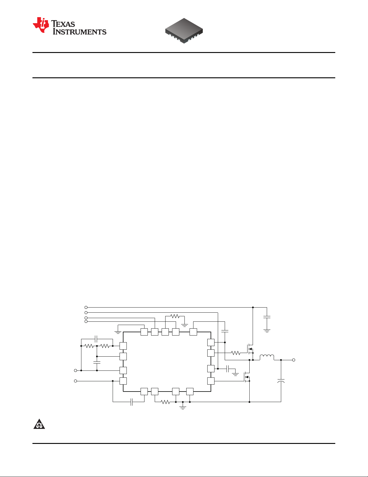
High Performance, Single-Synchronous Step-Down Controller
with Differential Voltage Feedback
1
FEATURES
23
• Differential Voltage Feedback
• DC Compensation for Accurate Regulation
• Wide Input Voltage Range: 3 V to 28 V
• Output Voltage Range: 0.5 V to 2.0 V with
Fixed Options of 1.05 V and 1.00 V
• Wide Output Load Range: 0 A to 20 A+
• Adaptive On-Time Modulation with Selectable
Control Architecture and Frequency
– D-CAP™ Mode at 300 kHz/400 kHz for Fast
Transient Response
– D-CAP2™ Mode at 500 kHz/670 kHz for
Ceramic Output Capacitor
• 4700 ppm/°C, Low-Side R
• R
Accurate Current Sense Option
SENSE
• Internal, 1-ms Voltage Servo Softstart
• Built-In Output Discharge
• Power Good Output
• Integrated Boost Switch
• Built-In OVP/UVP/OCP
• Thermal Shutdown (Non-latched)
• 3 mm × 3 mm, 16-Pin, QFN (RTE) Package
APPLICATIONS
• Notebook Computers
• I/O Supplies
Current Sensing
DS(on)
TPS51219
SLUSAG1B –MARCH 2011– REVISED OCTOBER 2011
DESCRIPTION
The TPS51219 is a small-sized single buck controller
with adaptive on-time control. It provides a choice of
control modes (D-CAP™ or D-CAP2™) to meet a
wide range of system requirements. It is designed for
tight DC regulation requirements such as the VCCIO
application for Intel®notebooks. The performance
and flexibility of the TPS51219 makes it suitable for
low output voltage, high current, PC system power
rails and similar point-of-load (POL) power supplies.
Differential voltage feedback and the voltage
compensation function combine to provide high
precision power to load devices.
A small package, fixed voltage options and minimal
external component count saves cost and space,
while a dedicated EN pin and pre-set frequency
selections minimize design effort. The skip-mode at
light load condition, strong gate drivers, and low-side
FET R
operation over a broad load range. The external
resistor current sense option enables accurate
current sensing. The conversion input voltage (the
high-side FET drain voltage) ranges from 3 V to 28 V
and output voltage ranges from 0.5 V to 2.0 V. The
device requires an external 5-V supply.
The TPS51219 is available in a 16-pin, QFN package
and is specified for ambient temperature from -40°C
to 85°C.
current sensing provides high efficiency
DS(on)
1
2D-CAP, D-CAP2 are trademarks of Texas Instruments.
3Intel is a registered trademark of Intel.
PRODUCTION DATA information is current as of publication date.
Products conform to specifications per the terms of the Texas
Instruments standard warranty. Production processing does not
necessarily include testing of all parameters.
Please be aware that an important notice concerning availability, standard warranty, and use in critical applications of Texas
Instruments semiconductor products and disclaimers thereto appears at the end of this data sheet.
Copyright © 2011, Texas Instruments Incorporated
TPS51219
SLUSAG1B –MARCH 2011– REVISED OCTOBER 2011
These devices have limited built-in ESD protection. The leads should be shorted together or the device placed in conductive foam
during storage or handling to prevent electrostatic damage to the MOS gates.
www.ti.com
ORDERING INFORMATION
T
A
PACKAGE PINS
–40°C to 85°C Plastic Quad Flat Pack (QFN) 16
ORDERABLE DEVICE OUTPUT MINIMUM
NUMBER SUPPLY QUANTITY
TPS51219RTER Tape and reel 3000
TPS51219RTET Mini-reel 250
(1)
(1) For the most current package and ordering information see the Package Option Addendum at the end of this document, or see the TI
web site at www.ti.com.
ABSOLUTE MAXIMUM RATINGS
(1)
over operating free-air temperature range (unless otherwise noted)
VALUE UNIT
MIN MAX
BST –0.3 36
(3)
BST
SW –5 30
Input voltage range
(2)
EN, MODE, TRIP, V5 –0.3 6.0 V
COMP, REFIN, VSNS –0.3 3.6
GSNS –0.35 0.35
PGND –0.3 0.3
DH –5 36
(3)
DH
Output voltage range
(2)
DL –0.3 6 V
PGOOD –0.3 6
VREF –0.3 3.6
Junction temperature range, T
Storage temperature range, T
J
STG
(1) Stresses beyond those listed under absolute maximum ratings may cause permanent damage to the device. These are stress ratings
only and functional operation of the device at these or any other conditions beyond those indicated under recommended operating
conditions is not implied. Exposure to absolute-maximum-rated conditions for extended periods may affect device reliability.
(2) All voltage values are with respect to the network ground terminal unless otherwise noted.
(3) Voltage values are with respect to the SW terminal.
–0.3 6
–0.3 6
125 °C
–55 150 °C
2 Submit Documentation Feedback Copyright © 2011, Texas Instruments Incorporated
TPS51219
www.ti.com
RECOMMENDED OPERATING CONDITIONS
Supply voltage V5 4.5 5.5 V
BST –0.1 33.5
(1)
BST
SW -3 28
(2)
Input voltage range V
Output voltage range V
T
A
(1) Voltage values are with respect to the SW terminal.
(2) This voltage should be applied for less than 30% of the repetitive period.
SW
EN, TRIP, MODE –0.1 5.5
REFIN, VSNS, COMP –0.1 3.5
GSNS –0.3 0.3
PGND –0.1 0.1
DH –3 33.5
(1)
DH
(2)
DH
DL –0.1 5.5
PGOOD –0.1 5.5
VREF –0.1 3.5
Operating free-air temperature –40 85 °C
SLUSAG1B –MARCH 2011– REVISED OCTOBER 2011
MIN TYP MAX UNIT
–0.1 5.5
–4.5 28
–0.1 5.5
–4.5 33.5
THERMAL INFORMATION
TPS51219
THERMAL METRIC
θ
θ
θ
ψ
ψ
θ
JA
JCtop
JB
JT
JB
JCbot
Junction-to-ambient thermal resistance
Junction-to-case (top) thermal resistance
Junction-to-board thermal resistance
Junction-to-top characterization parameter
Junction-to-board characterization parameter
Junction-to-case (bottom) thermal resistance
(1) For more information about traditional and new thermal metrics, see the IC Package Thermal Metrics application report, SPRA953.
(2) The junction-to-ambient thermal resistance under natural convection is obtained in a simulation on a JEDEC-standard, high-K board, as
specified in JESD51-7, in an environment described in JESD51-2a.
(3) The junction-to-case (top) thermal resistance is obtained by simulating a cold plate test on the package top. No specific
JEDEC-standard test exists, but a close description can be found in the ANSI SEMI standard G30-88.
(4) The junction-to-board thermal resistance is obtained by simulating in an environment with a ring cold plate fixture to control the PCB
temperature, as described in JESD51-8.
(5) The junction-to-top characterization parameter, ψJT, estimates the junction temperature of a device in a real system and is extracted
from the simulation data for obtaining θJA, using a procedure described in JESD51-2a (sections 6 and 7).
(6) The junction-to-board characterization parameter, ψJB, estimates the junction temperature of a device in a real system and is extracted
from the simulation data for obtaining θJA, using a procedure described in JESD51-2a (sections 6 and 7).
(7) The junction-to-case (bottom) thermal resistance is obtained by simulating a cold plate test on the exposed (power) pad. No specific
JEDEC standard test exists, but a close description can be found in the ANSI SEMI standard G30-88.
(1)
RTE UNITS
16 PINS
(2)
(3)
(4)
(5)
(6)
(7)
48.5
49.5
22.1
0.7
22.1
7.1
°C/W
Copyright © 2011, Texas Instruments Incorporated Submit Documentation Feedback 3
TPS51219
SLUSAG1B –MARCH 2011– REVISED OCTOBER 2011
ELECTRICAL CHARACTERISTICS
over operating free-air temperature range, VV5= 5 V, V
PARAMETER TEST CONDITION MIN TYP MAX UNIT
SUPPLY CURRENT
I
V5
I
V5SDN
VREF OUTPUT
V
VREF
V
VREF(tol)
I
VREF(ocl)
OUTPUT VOLTAGE
V
VSNS
V
VSNS(tol)
V
REFIN1
V
REFIN1P05
V
OFF_LPCMP
V
COMPCLP
g
M
I
VSNS
I
REFIN
I
VSNS(dis)
SWITCH MODE POWER SUPPLY (SMPS) FREQUENCY
f
SW
t
ON(min)
t
OFF(min)
MOSFET DRIVERS
R
DH
R
DL
t
DEAD
INTERNAL BOOT STRAP SWITCH
V
FBST
I
BSTLK
(1) Ensured by design. Not production tested.
V5 supply current TA= 25°C, No load, VEN= 5 V 560 μA
V5 shutdown current TA= 25°C, No load, VEN= 0 V 0.5 2.0 μA
Output voltage I
Output voltage tolerance
Current limit V
VSNS sense voltage V
VSNS regulation voltage tolerance V
= 0 μA wrt GSNS 2.000 V
VREF
0 μA ≤ I
VREF
0 μA ≤ I
VREF
VREF-GSNS
V
= 0 V 1.000 V
REFIN
= 3.3 V 1.050 V
REFIN
0.5 V ≤ V
REFIN
V
= 0 V, 0°C ≤ TA≤ 85°C –9 9
REFIN
V
= 0 V, -40°C ≤ TA≤ 85°C -14 14
REFIN
= 3.3 V, 0°C ≤ TA≤ 85°C –9 9 mV
REFIN
V
= 3.3 V, -40°C ≤ TA≤ 85°C -14 14
REFIN
V
= 0.5 V and V
REFIN
REFIN voltage for 1.00-V output 0.3 V
REFIN voltage for 1.05-V output 2.2 V
Loop comparator offset voltage V
COMP clamp voltage
Error amplifier transconductance V
VSNS input current V
REFIN input current V
= 1 V, VSNS shorted to COMP -5 5 mV
REFIN
V
= 0 V, V
REFIN
V
= 0 V, V
REFIN
= 0 V 130 μS
REFIN
= 1.05 V -1 1 μA
VSNS
= 0 V –1 1 μA
REFIN
VSNS discharge current VEN= 0 V, V
VIN= 12 V, V
Switching frequency kHz
VIN= 12 V, V
VIN= 12 V, V
VIN= 12 V, V
Minimum on time DH rising to falling
Minimum off time DH falling to rising 320
DH resistance
DL resistance
Dead time ns
Forward voltage V
Source, IDH= –50 mA 1.6 3.0
Sink, IDH= 50 mA 0.6 1.5
Source, IDL= –50 mA 0.9 2.0
Sink, IDL= 50 mA 0.5 1.2
DH-off to DL-on 10
DL-off to DH-on 20
, TA= 25°C, IF= 10 mA 0.1 0.2 V
V5-BST
BST leakage current TA= 25°C, V
www.ti.com
= 0 V, VEN= 5 V (unless otherwise noted)
MODE
< 30 μA, TA= 0°C to 85°C -0.8% 0.8%
< 300 μA, TA= –40°C to 85°C -1.2% 1.2%
= 1.7 V 0.4 1.0 mA
≤ 2 V V
= 2.0 V -5 5
REFIN
= 0.95 V 0.885 V
VSNS
= 1.05 V 1.115 V
VSNS
= 0.5 V 5 12 mA
VSNS
VSNS
VSNS
VSNS
VSNS
= 1.8 V, V
= 1.8 V, V
= 1.8 V, V
= 1.8 V, V
(1)
= 2.5 V 400
MODE
= 1.67 V 300
MODE
= 0.2 V 670
MODE
= 0.033 V 500
MODE
REFIN
60
V
ns
Ω
= 33 V, VSW= 28 V 0.01 1.5 μA
BST
4 Submit Documentation Feedback Copyright © 2011, Texas Instruments Incorporated
www.ti.com
ELECTRICAL CHARACTERISTICS (continued)
over operating free-air temperature range, VV5= 5 V, V
PARAMETER TEST CONDITION MIN TYP MAX UNIT
LOGIC THRESHOLD
I
MODE
V
THMODE
V
LL
V
LH
V
LHYST
I
LLK
SOFT START
t
SS
POWERGOOD COMPARATOR
V
THPG
I
PG
t
PGDLY
t
PGCMPSS
I
PG(leak)
CURRENT DETECTION
I
TRIP
(2)
TC
ITRIP
V
TRIP
V
OCL
V
OCLN
V
RTRIP
V
ZC
(2) Ensured by design. Not production tested.
MODE source current 15.6 16.7 17.8 μA
MODE 0-1 113 143 173
MODE 1-2 253 283 313
MODE 2-3 433 458 483
MODE threshold voltage MODE 3-4 644 667 690 mV
MODE 4-5 914 949 984
MODE 5-6 1329 1369 1409
MODE 6-7 1950 2000 2050
EN low-level voltage 0.5
EN high-level voltage 1.8 V
EN hysteresis voltage 0.25
EN input leakage current –1 0 1 μA
Soft-start time Internal soft-start time 1.1 ms
PGOOD in from higher 106% 108% 110%
PGOOD threshold
PGOOD in from lower 90% 92% 94%
PGOOD out to higher 114% 116% 118%
PGOOD out to lower 82% 84% 86%
PGOOD sink current V
PGOOD delay time
PGOOD
Delay for PGOOD in 0.8 1.0 1.2 ms
Delay for PGOOD out, with 100 mV over drive 0.25 µs
PGOOD start-up delay PGOOD comparator wake-up delay 2.5 ms
PGOOD leakage current -1 0 1 µA
TRIP source current TA= 25°C, V
TRIP source current temperature
coefficient
V
(2)
voltage range R
TRIP
Current limit threshold V
Negative current limit threshold V
R
V
V
V
V
DS(on)
DS(on)
TRIP
TRIP
TRIP
TRIP
TRIP
TRIP
Resistor sense trip voltage Resistor sensing 25 mV
Zero cross detection offset 0 mV
MODE
= 0.5 V 3 6 mA
TRIP
sensing 4700 ppm/°C
sensing 0.2 3 V
= 3.0 V, R
= 1.6 V, R
= 0.2 V, R
= 3.0 V, R
= 1.6 V, R
= 0.2 V, R
DS(on)
DS(on)
DS(on)
DS(on)
DS(on)
DS(on)
TPS51219
SLUSAG1B –MARCH 2011– REVISED OCTOBER 2011
= 0 V, VEN= 5 V (unless otherwise noted)
= 0.4 V, R
sensing 360 375 390
sensing 190 200 210 mV
sensing 20 25 30
sensing –390 –375 –360
sensing –212 –200 –188 mV
sensing –30 –25 –20
sensing 9 10 11 μA
DS(on)
Copyright © 2011, Texas Instruments Incorporated Submit Documentation Feedback 5
TPS51219
SLUSAG1B –MARCH 2011– REVISED OCTOBER 2011
ELECTRICAL CHARACTERISTICS (continued)
over operating free-air temperature range, VV5= 5 V, V
PARAMETER TEST CONDITION MIN TYP MAX UNIT
PROTECTIONS
V
UVLO
V
OVP
t
OVPDLY
V
UVP
t
UVPDLY
t
UVPENDLY
V5 UVLO threshold voltage V
OVP threshold voltage OVP detect voltage 118% 120% 122%
OVP propagation delay With 100 mV over drive 370 ns
UVP threshold voltage UVP detect voltage 66% 68% 70%
UVP delay 1 ms
UVP enable delay 1.4 ms
THERMAL SHUTDOWN
T
SDN
Thermal shutdown threshold °C
(3) Ensured by design. Not production tested.
Wake-up 4.2 4.4 4.5
Shutdown 3.7 3.9 4.1
Shutdown temperature
Hysteresis
MODE
(3)
= 0 V, VEN= 5 V (unless otherwise noted)
(3)
www.ti.com
140
10
6 Submit Documentation Feedback Copyright © 2011, Texas Instruments Incorporated
4
2
3
8
12
11
10
9
VREF
REFIN
GSNS
VSNS
PGOOD
DH
DL
V5
16 15 14 13
1
5 6 7
MODE
EN
BST
SW
PGND
GND
COMP
TRIP
TPS51219
PowerPAD
TM
www.ti.com
TPS51219
SLUSAG1B –MARCH 2011– REVISED OCTOBER 2011
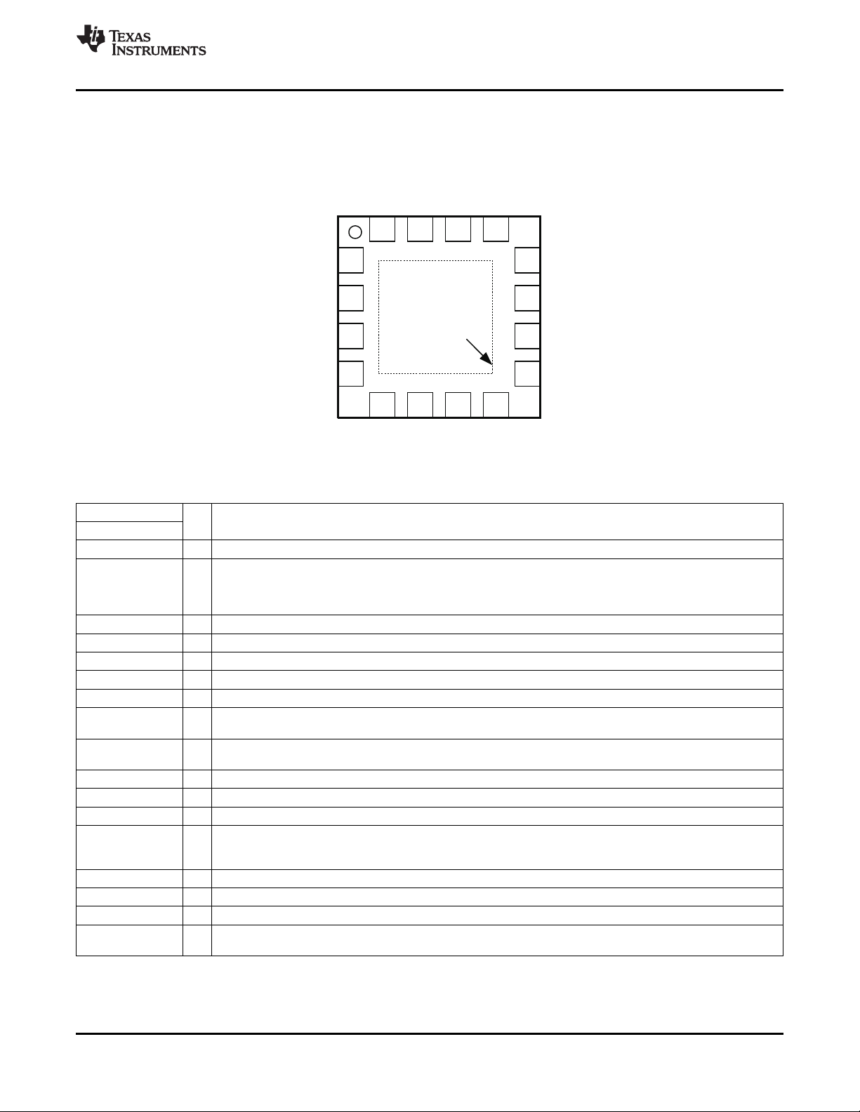
DEVICE INFORMATION
RTE PACKAGE (TOP VIEW)
PIN FUNCTIONS
PIN
NAME NO.
BST 13 I High-side MOSFET gate driver bootstrap voltage input. Connect a capacitor from the BST pin to the SW pin.
COMP 5 I
DH 11 O High-side MOSFET gate driver output.
DL 10 O Low-side MOSFET gate driver output.
EN 14 I Enable pin. 3.3-V I/O level, 100 ns de-bounce. Short to GND to disable the device.
GND 7 – Device analog ground; Connect to a quiet point on the system GND plane
GSNS 3 I Voltage sense return tied directly to the GND sense point of the load. Short to GND if remote sense is not used.
MODE 15 I
PGND 8 –
PGOOD 16 O Powergood signal open drain output. PGOOD goes high when the output voltage is within the target range.
REFIN 2 I Output voltage setting pin. See the VREF and REFIN, Output Voltage section.
SW 12 I/O High-side MOSFET gate driver return. R
TRIP 6 I current sensing if connected to GND through an OCL setting resistor. For R
VSNS 4 I Voltage sense line tied directly to the load voltage sense point.
VREF 1 O 2.0-V ±0.8% voltage reference output.
V5 9 I 5V power supply input for internal circuits and MOSFET gate drivers.
Thermal
pad
I/O DESCRIPTION
Connection for the DC compensation integrator for improved load-line performance. Connect a capacitor from
this pin to the VSNS pin (when operating in D-CAP2 mode), or to the positive terminal of the output capacitor
(when operating in D-CAP mode). Connect directly to the VSNS pin without capacitor to disable the integrator
function.
Connect a resistor to GND to configure switching frequency, control mode and current sense scheme. (See
Table 2)
Synchronous low-side MOSFET gate driver return. Also serve as the current sensing input (+). Connect to the
GND pin as close as possible to the device.
current sensing input (–) when using R
DS(on)
Current sense comparator input (-) for resistor current sensing. Or overcurrent threshold setting pin for R
μA at room temperature, TC=4700ppm/°C, is sourced to set the trip voltage.
– – Thermal pad. Connect directly to system GND plane with multiple vias.
current sensing.
DS(on)
current sensing operation, 10
DS(on)
DS(on)
Copyright © 2011, Texas Instruments Incorporated Submit Documentation Feedback 7
8
12
PGND
SW
OC
ZC
XCON
13
BST
9 V5
PWM
4
REFIN
TRIP
Delay
16 PGOOD
Control Logic
10 mA
+
+
V
REFIN
+ 20%
+
+
2
VSNS
6
11 DH
10 DL
t
ON
OneShot
UV
OV
V
REFIN
– 32%
14EN
Soft-Start
+
NOC
+
1VREF Reference
7 R
R
Control Mode
On-Time
Current Sense
Selection
16.7 mA
15 MODE
V
REFIN
+8/16%
V
REFIN
– 8/16%
+
+
Discharge
V5OK
+
4.3 V/3.9 V
UVPOVP
COMP 5
+
VBG
5-V UVLO
TPS51219
UDG-11007
EN
3GSNS
7GND
EN
Set_1p05v
Set_adj
Discharge
R
8 R
+
V
REFIN
2.2 V
0.3 V
Set_adj
Set_1p05v
EN
+
+
25 mV
Set_resistor _sensing
Set_resistor _sensing
TPS51219
SLUSAG1B –MARCH 2011– REVISED OCTOBER 2011
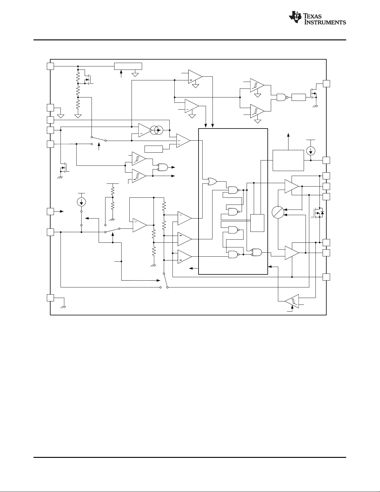
FUNCTIONAL BLOCK DIAGRAM
www.ti.com
8 Submit Documentation Feedback Copyright © 2011, Texas Instruments Incorporated
0
200
400
600
800
1000
−50 −25 0 25 50 75 100 125
Junction Temperature (°C)
V5 Supply Current (µA)
VV5 = 5 V
VEN = 5 V
No Load
0
2
4
6
8
10
−50 −25 0 25 50 75 100 125
Junction Temperature (°C)
V5 Shutdown Current (µA)
VV5 = 5 V
VEN = 0 V
No Load
0
2
4
6
8
10
12
14
16
−50 −25 0 25 50 75 100 125
Junction Temperature (°C)
Trip Source Current (µA)
VV5 = 5 V
V
TRIP
= 0.5 V
50
60
70
80
90
100
110
120
130
140
150
−50 −25 0 25 50 75 100 125
Junction Temperature (°C)
UVP/OVP Threshold (%)
UVP
OVP
VV5 = 5 V
V
REFIN
= 0 V
1.980
1.985
1.990
1.995
2.000
2.005
2.010
2.015
2.020
0 50 100 150 200 250 300 350 400
VREF Current (µA)
VREF Voltage (V)
VV5 = 5 V
TA = 27°C
200
300
400
500
600
700
800
900
6 8 10 12 14 16 18 20 22
Input Voltage (V)
Switching Frequency (kHz)
R
MODE
= 1 kΩ
R
MODE
= 12 kΩ
R
MODE
= 100 kΩ
R
MODE
= 200 kΩ
I
OUT
= 10 A
www.ti.com
TPS51219
SLUSAG1B –MARCH 2011– REVISED OCTOBER 2011
TYPICAL CHARACTERISTICS
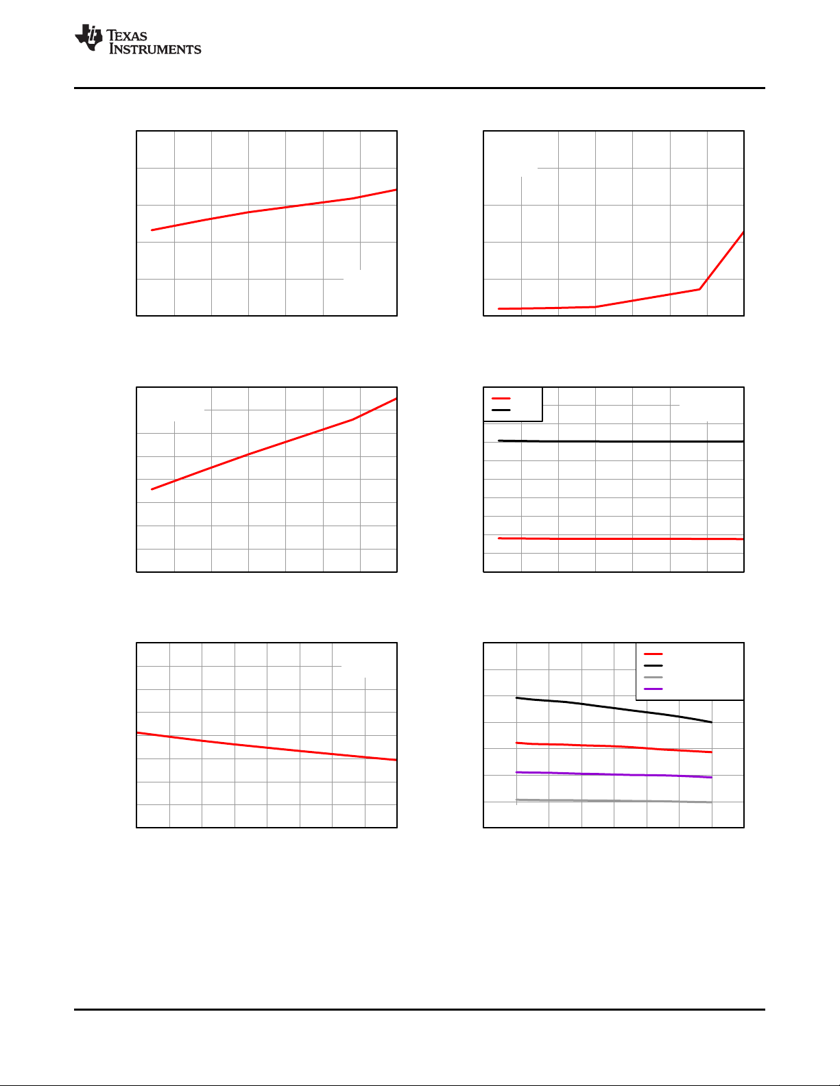
Figure 1. V5 Supply Current vs Junction Temperature Figure 2. V5 Shutdown Current vs Junction Temperature
Figure 3. Current Sense Current vs Junction Temperature Figure 4. OVP/UVP Threshold vs Junction Temperature
Copyright © 2011, Texas Instruments Incorporated Submit Documentation Feedback 9
Figure 5. VREF Load Regulation Figure 6. Switching Frequency vs Input Voltage
0
100
200
300
400
500
600
700
800
0 2 4 6 8 10 12 14 16 18 20
Output Current (A)
Switching Frequency (kHz)
R
MODE
= 100 kΩ
VIN = 12 V
V
OUT
= 1.05 V
L = 0.56 µH
0
100
200
300
400
500
600
700
800
0 2 4 6 8 10 12 14 16 18 20
Output Current (A)
Switching Frequency (kHz)
R
MODE
= 200 kΩ
VIN = 12 V
V
OUT
= 1.05 V
L = 0.56 µH
0
100
200
300
400
500
600
700
800
0 2 4 6 8 10 12 14 16 18 20
Output Current (A)
Switching Frequency (kHz)
R
MODE
= 1 kΩ
VIN = 12 V
V
OUT
= 1.05 V
L = 0.45 µH
0
100
200
300
400
500
600
700
800
0 2 4 6 8 10 12 14 16 18 20
Output Current (A)
Switching Frequency (kHz)
R
MODE
= 12 kΩ
VIN = 12 V
V
OUT
= 1.05 V
L = 0.36 µH
1.030
1.035
1.040
1.045
1.050
1.055
1.060
1.065
1.070
0 2 4 6 8 10 12 14 16 18 20
1.05−V Output Current (A)
VSNS−GSNS − 1.05−V Output Voltage (V)
R
MODE
= 1 kΩ
VIN = 12 V
G001
1.030
1.035
1.040
1.045
1.050
1.055
1.060
1.065
1.070
6 8 10 12 14 16 18 20 22
Input Voltage (V)
VSNS−GSNS − 1.05−V Output Voltage (V)
I
OUT
= 0 A
I
OUT
= 10 A
R
MODE
= 1 kΩ
G001
TPS51219
SLUSAG1B –MARCH 2011– REVISED OCTOBER 2011
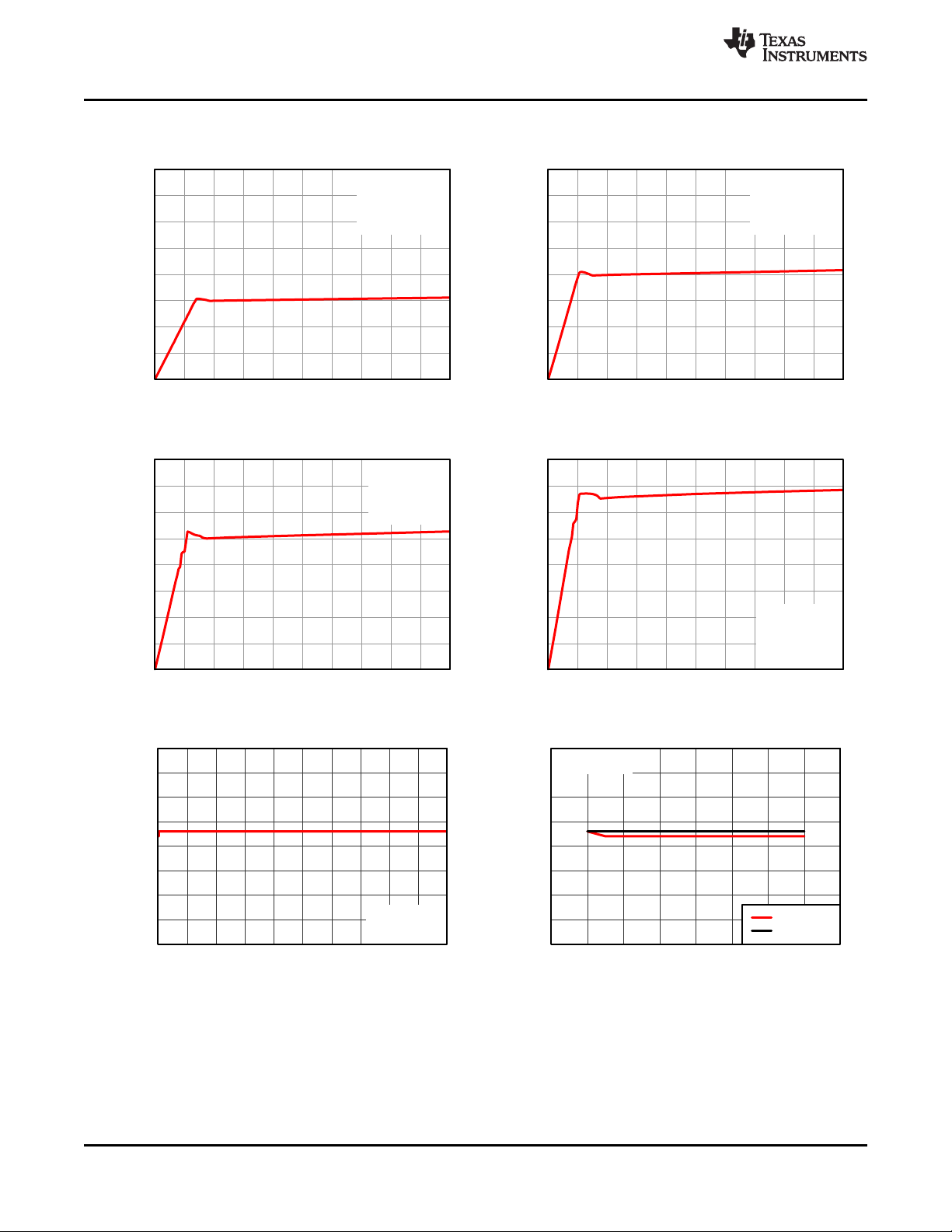
Figure 11 and Figure 12 refer to the application schematic in Figure 33.
Figure 7. Switching Frequency vs Load Current Figure 8. Switching Frequency vs Load Current
www.ti.com
TYPICAL CHARACTERISTICS
Figure 9. Switching Frequency vs Load Current Figure 10. Switching Frequency vs Load Current
10 Submit Documentation Feedback Copyright © 2011, Texas Instruments Incorporated
Figure 11. 1.05-V Output Load Regulation Figure 12. 1.05-V Output Line Regulation
0.980
0.985
0.990
0.995
1.000
1.005
1.010
1.015
1.020
0 2 4 6 8 10
1.00−V Output Current (A)
VSNS−GSNS − 1.00−V Output Voltage (V)
R
MODE
= 1 kΩ
VIN = 12 V
G001
0
10
20
30
40
50
60
70
80
90
100
0.001 0.01 0.1 1 10 100
1.05−V Output Current (A)
Efficiency (%)
VIN = 8 V
VIN = 12 V
VIN = 20 V
R
MODE
= 1 kΩ
0.980
0.985
0.990
0.995
1.000
1.005
1.010
1.015
1.020
6 8 10 12 14 16 18 20 22
Input Voltage (V)
VSNS−GSNS − 1.00−V Output Voltage (V)
I
OUT
= 0 A
I
OUT
= 10 A
R
MODE
= 1 kΩ
G001
0
10
20
30
40
50
60
70
80
90
100
0.001 0.01 0.1 1 10 100
1.00−V Output Current (A)
Efficiency (%)
VIN = 8 V
VIN = 12 V
VIN = 20 V
R
MODE
= 1 kΩ
www.ti.com
TPS51219
SLUSAG1B –MARCH 2011– REVISED OCTOBER 2011
TYPICAL CHARACTERISTICS
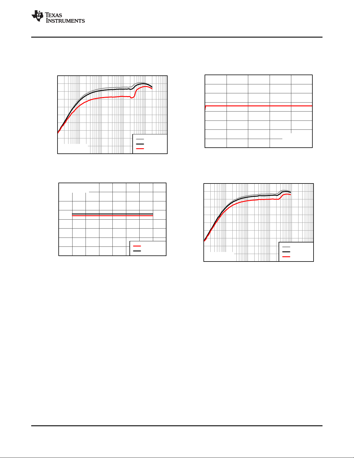
Figure 11, Figure 12, and Figure 13 refer to the application schematic in Figure 33.
Figure 14, Figure 15 and Figure 16, refer to the application schematic in Figure 33 except the parameters
of L1 (0.56 µH), C7 (2 × 330 µF) and Q3 (not used).
Figure 13. 1.05-V Output Efficiency Figure 14. 1.00-V Output Load Regulation
Figure 15. 1.00-V Output Line Regulation Figure 16. 1.00-V Output Efficiency
Copyright © 2011, Texas Instruments Incorporated Submit Documentation Feedback 11
VIN=20 V
VSNS-GSNS (20 mV/div)
offset: 1.05 V
I
OUT
(8 A/div)
offset: 6 A
C
OUT
= 5 x 330 µF(Bulk) + 12 x 22 µF(MLCC)
VIN=20 V
VSNS-GSNS (20 mV/div)
offset: 1.00 V
I
OUT
(8 A/div)
C
OUT
= 2 x 330 µF(Bulk) + 12 x 22 µF(MLCC)
EN (5 V/div)
VSNS-GSNS
(500mV/div)
PGOOD (5V/div)
Time (400 µs/div)
I
OUT
= 15A
Time (400 µs/div)
EN (5 V/div)
VSNS-GSNS
(500mV/div)
PGOOD (5V/div)
I
OUT
= 0 A
0.5-V Pre-biased
TPS51219
SLUSAG1B –MARCH 2011– REVISED OCTOBER 2011
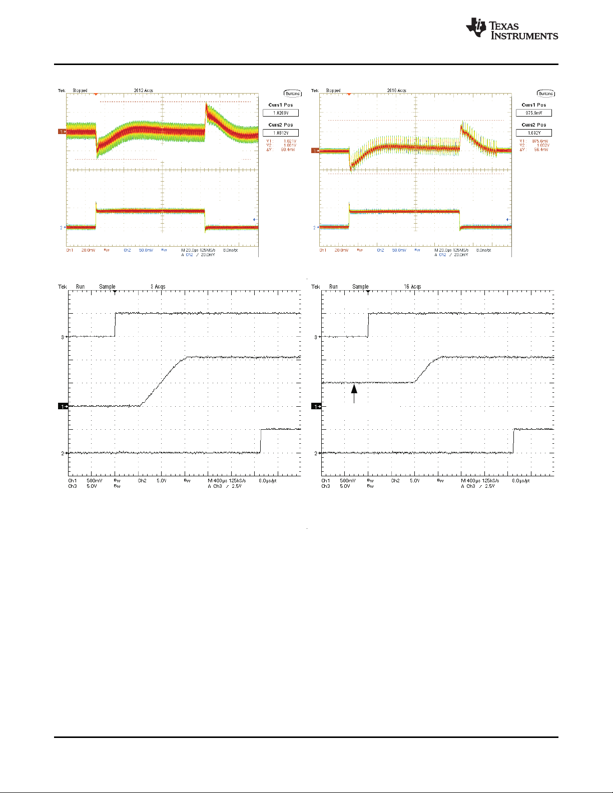
Figure 17. 1.05-V Load Transient Response Figure 18. 1.00-V Load Transient Response
www.ti.com
TYPICAL CHARACTERISTICS
12 Submit Documentation Feedback Copyright © 2011, Texas Instruments Incorporated
Figure 19. 1.05-V Startup Waveforms Figure 20. 1.05-V Startup Waveforms (0.5-V Pre-Biased)

Time (100 ms/div)
EN (5 V/div)
VSNS-GSNS
(500mV/div)
PGOOD (5V/div)
I
OUT
= 0 A
100 1000 10000 100000 1000000
−80
−60
−40
−20
0
20
40
60
80
−180
−135
−90
−45
0
45
90
135
180
Frequency (Hz)
Gain (dB)
Phase (°)
Gain
Phase
VIN =12 V
I
OUT
=15 A
R
MODE
=1 kΩ
www.ti.com
TPS51219
SLUSAG1B –MARCH 2011– REVISED OCTOBER 2011
TYPICAL CHARACTERISTICS
Figure 22 refers to application schematic of Figure 33.
Figure 21. 1.05-V Soft-stop Waveforms
Figure 22. Bode Plot, V
OUT
=1.05 V
Copyright © 2011, Texas Instruments Incorporated Submit Documentation Feedback 13

TPS51219
1
2
3
VREF
GSNS
REFIN
R1
10 nF
R2
0,1 mF
UDG-11042
TPS51219
SLUSAG1B –MARCH 2011– REVISED OCTOBER 2011
APPLICATION INFORMATION
Swtich Mode Power Supply Control
The TPS51219 is a high performance, single-synchronous step-down controller with differential voltage feedback.
The TPS51219 realizes accurate regulation at the specific load point over wide load range with the combination
of three functions.
• 2-V Reference with 0.8% Tolerance. Internal voltage divider provides precise reference (See Table 1 in the
VREF and REFIN, Output Voltage section). A value of 0.1µF is recommended as the decoupling capacitance
between VREF and GSNS pins.
• Integrator. Feedback capacitance connected from the output (COMP pin) to the input (VSNS pin) of the error
amplifier comprises integrator, which increases gain at DC to low frequency region and improves load
regulation of the output voltage. 10nF is recommended as the capacitance between VSNS and COMP pins.
• Differential remote sensing. Differential feedback provides precise output voltage control at the point of
load. Connect VSNS and GSNS directly to output voltage sense point and ground return point at the load
device, respectively. Short GSNS to GND if remote sense is not used.
The TPS51219 supports two control architectures, D-CAP™ mode and D-CAP2™ mode. Both control modes do
not require complex external compensation networks and are suitable for designs with small external
components counts. The D-CAP™ mode provides fast transient response with appropriate amount of equivalent
series resistance (ESR) on the output capacitors. The D-CAP2™ mode is dedicated for a configuration with very
low ESR output capacitors such as multi-layer ceramic capacitors (MLCC). For the both modes, an adaptive
on-time control scheme is used to achieve pseudo-constant frequency. The TPS51219 adjusts the on-time (tON)
to be inversely proportional to the input voltage (VIN) and proportional to the SMPS output voltage (V
switching frequency remains nearly constant over the variation of input voltage at the steady-state condition.
Control modes and switching frequency are selected by the MODE pin described in Table 2.
www.ti.com
). The
OUT
VREF and REFIN, Output Voltage
The device provides a 2.0-V, ±0.8% accurate, voltage reference from VREF. This output has a 300-µA current
capability to drive the REFIN input voltage through a voltage divider circuit. A capacitor with a value of 0.1-µF or
larger should be attached close to the VREF terminal.
The SMPS output voltage is defined by REFIN voltage, within the range between 0.5 V and 2.0 V, programmed
by the resister-divider connected between VREF and GSNS. (See Figure 23 and External Components Selection
section.) A few nano-farads of capacitance from REFIN to GSNS is recommended for stable operation. A voltage
divider and a filter capacitor to this pin should be referenced to GSNS. Fixed output voltage can be set as shown
in Table 1.
XXXX
Table 1. Output Voltage Selection
REFIN VOLTAGE (V) OUTPUT VOLTAGE (V)
3.3 1.05
GSNS 1.00
Resistor Divider Adjustable
XXXX
XXXX
XXXX
Figure 23. Voltage Reference Connections
XXXX
XXXX
14 Submit Documentation Feedback Copyright © 2011, Texas Instruments Incorporated

700 ms400 ms 1.4 ms
EN
VREF
V
OUT
PGOOD
UDG-11008
TPS51219
www.ti.com
Soft-Start and Powergood
Provide a voltage supply to VIN and V5 before asserting EN to high. TPS51219 provides integrated soft-start
functions to suppress in-rush current at start-up. The soft-start is achieved by controlling internal reference
voltage ramping up. Figure 24 shows the start-up waveforms. The switching regulator waits for 400μs after EN
assertion. The MODE pin voltage is read in this period. A typical V
THe TPS51219 has a powergood open-drain output that indicates the V
The target voltage window and transition delay times of the PGOOD comparator are ±8% (typ) and 1-ms delay
for assertion (low to high), and ±16% (typ) and 2-µs delay for de-assertion (high to low) during running. The
PGOOD start-up delay is 2.5 ms after EN is asserted to high. The time constant, which is composed of the
REFIN capacitor and a resistor divider, needs to be short enough to reach the target value before PGOOD
comparator enabled.
OUT
SLUSAG1B –MARCH 2011– REVISED OCTOBER 2011
ramp up duration is 700 μs.
voltage is within the target range.
OUT
Figure 24. Typical Start-up Waveforms
MODE Pin Configuration
The TPS51219 reads the MODE pin voltage when the EN signal is raised high and stores the status in a
register. A 16.7-μA current is sourced from the MODE pin during this time to read the voltage across the resistor
connected between the pin and GND. Table 2 shows resistor values, corresponding control mode, switching
frequency and current sense operation configurations.
Table 2. MODE Selection
MODE NO.
7 200 400
6 100 300
5 68 300
4 47 400
3 33 500
2 22 670
1 12 670
0 1 500
Copyright © 2011, Texas Instruments Incorporated Submit Documentation Feedback 15
RESISTANCE BETWEEN CONTROL SWITCHING CURRENT SENSE
MODE AND GND (kΩ ) MODE FREQUENCY (kHz) OPERATION
R
DS(on)
D-CAP™
Resistor
Resistor
D-CAP2™
R
DS(on)

4
+
2
gM=130 mS
VSNS
REFIN
1
VREF
Control
Logic
and
Driver
R1
R2
11
10
DH
DL
+
2.0 V
V
IN
Lx
ESR
C
OUT
R
LOAD
UDG-11009
V
OUT
5
COMP
C1
+
PWM
= £
p´ ´
SW
0
OUT
f
1
f
2 ESR C 3
£
p´
f
0
M
g
2 C1 10
TPS51219
SLUSAG1B –MARCH 2011– REVISED OCTOBER 2011
D-CAP™ Mode
Figure 25 shows a simplified model of D-CAP™ mode architecture in the TPS51219.
Figure 25. Simplified D-CAP™ Model
www.ti.com
The transconductance amplifier and the capacitance C1 configure an integrator. The VSNS voltage is compared
with REFIN voltage. Ripple voltage generated by ESR of the output capacitance is fed back through the C1 so
that C1 should be properly connected to the positive terminal of output capacitor, not at the remote point of load.
The PWM comparator creates a set signal to turn on the high-side MOSFET each cycle. The D-CAP™ mode
offers flexibility on output inductance and capacitance selections with ease-of-use without complex feedback loop
calculation and external components. However, it does require sufficient amount of ESR that represents inductor
current information for stable operation and good jitter performance. Organic semiconductor capacitor(s) or
specialty polymer capacitor(s) are recommended.
The requirement for loop stability is simple and is described in Equation 1. The 0-dB frequency, f0, is
recommended to be lower than 1/3 of the switching frequency to secure proper phase margin. The integrator
time constant should be long enough compared to f0, for example one decade low, as described in Equation 2.
where
• ESR is the effective series resistance of the output capacitor
• C
• fSWis the switching frequency (1)
where
• gMis transconductance of the error amplifier (typically 130 µS) (2)
16 Submit Documentation Feedback Copyright © 2011, Texas Instruments Incorporated
is the capacitance of the output capacitor
OUT

V
VSNS
V
REFIN
(1)
(2)
t
ON
t
OFF
Slope (2)
Jitter
20 mV
Slope (1)
Jitter
UDG-11010
V
REFIN
+Noise
Time
´
³
´
OUT
SW X
V ESR
20mV
f L
TPS51219
www.ti.com
Jitter is another attribute caused by signal-to-noise ratio of the feedback signal. One of the major factors that
determine jitter performance in D-CAP™ mode is the down-slope angle of the VSNS ripple voltage. Figure 26
shows, in the same noise condition, that jitter is improved by making the slope angle larger.
SLUSAG1B –MARCH 2011– REVISED OCTOBER 2011
Figure 26. Ripple Voltage Slope and Jitter Performance
For a good jitter performance, use the recommended down slope of approximately 20 mV per switching period as
shown in Figure 26 and Equation 3.
where
• V
• LXis the inductance (3)
is the SMPS output voltage
OUT
Copyright © 2011, Texas Instruments Incorporated Submit Documentation Feedback 17

PWM
Comparator
Control
Logic
and
Driver
L
X
R
LOAD
UDG-11011
4
C
C1
V
IN
11
10
DH
DL
VSNS
G
2
REFIN
1
VREF
+
2.0 V
+
–
+
R
C1
C
C2
R
C2
R1
R2
TPS51219
V
OUT
ESR
C
OUT
12
SW
+
5
COMP
C1
´
= £
p´ ´ ´
C C SW
0
X OUT
R C f
f
2 G L C 3
£
p´
f
0
M
g
2 C1 10
TPS51219
SLUSAG1B –MARCH 2011– REVISED OCTOBER 2011
D-CAP2™ Mode Operation
Figure 27 shows simplified model of D-CAP2™ architecture.
Figure 27. Simplified Modulator Using D-CAP2™ Mode
www.ti.com
When the TPS51219 operates in D-CAP2™ mode, connect the COMP and VSNS pins as shown in Figure 27.
The transconductance amplifier and the capacitance C1 configures the integrator. The D-CAP2™ mode in the
TPS51219 includes an internal feedback network enabling the use of very low ESR output capacitor(s) such as
multi-layer ceramic capacitors (MLCC). The role of the internal network is to sense the ripple component of the
inductor current information and then combine it with the voltage feedback signal.
Using RC1=RC2≡RCand CC1=CC2≡CC, 0-dB frequency of the D-CAP2™ mode is given by Equation 4. f0is
recommended to be lower than 1/3 of the switching frequency to secure proper phase margin. The integrator
time constant should be long enough compared to f0, for example one decade low, as described in Equation 5.
where
The typical G value is 0.25, and typical RCCCtime constant values for 500 kHz and 670 kHz operation are 32 μs
and 23 μs, respectively.
For example, when fSW= 500 kHz and LX=0.45 μH, C
capacitor, pay attention to its characteristics. For MLCC use X5R or better dielectric and take into account
derating of the capacitance by both DC bias and AC bias. When derating by DC bias and AC bias are 80% and
50%, respectively, the effective derating is 40% because 0.8 x 0.5 = 0.4. The capacitance of specialty polymer
capacitors may change depending on the operating frequency. Consult capacitor manufacturers for specific
characteristics.
18 Submit Documentation Feedback Copyright © 2011, Texas Instruments Incorporated
• G is gain of the amplifier which amplifies the ripple current information generated by the compensation
circuit (4)
should be larger than 272 μF. At the selection of
OUT
(5)

( )
-
= ´ ´
´
IN OUT
OUT
LOAD(LL)
X IN SW
V V
V
1
I
2 L V f
æ ö
= ´
ç ÷
è ø
TRIP
OCTRIP TRIP
I
V R
8
( ) ( )
æ ö æ ö
-
ç ÷ ç ÷
= + = + ´ ´
ç ÷ ç ÷
´
è ø è ø
IND(ripple)
OCTRIP OCTRIP IN OUT OUT
OCL
X SW IN
DS on DS on
I
V V V V V
1
I
R 2 R 2 L f V
TPS51219
www.ti.com
Light-Load Operation
In auto-skip mode, the TPS51219 SMPS control logic automatically reduces its switching frequency to improve
light-load efficiency. To achieve this intelligence, a zero cross detection comparator is used to prevent negative
inductor current by turning off the low-side MOSFET. Equation 6 shows the boundary load condition of this skip
mode and continuous conduction operation.
Current Sensing
In order to provide both cost effective solution and good accuracy, TPS51219 supports both of MOSFET R
sensing and external resistor sensing. For R
through the trip voltage setting resistor, R
. In this scheme, TRIP terminal sources 10µA of I
TRIP
the trip level is set to 1/8 of the voltage across the R
between the PGND pin and the SW pin so that the SW pin is connected to the drain terminal of the low-side
MOSFET. I
has a 4700ppm/°C temperature slope to compensate the temperature dependency of the R
TRIP
For resistor sensing scheme, an appropriate current sensing resistor should be connected between the source
terminal of the low-side MOSFET and PGND. The TRIP pin is connected to the MOSFET source terminal node.
The inductor current is monitored by the voltage between PGND pin and TRIP pin. In either scheme, PGND is
used as the positive current sensing node so that PGND should be connected to the proper current sensing
device, i.e. the sense resistor or the source terminal of the low-side MOSFET.
sensing scheme, TRIP pin should be connected to GND
DS(on)
. The inductor current is monitored by the voltage
TRIP
SLUSAG1B –MARCH 2011– REVISED OCTOBER 2011
(6)
DS(on)
current and
TRIP
DS(on)
.
Overcurrent Protection
TPS51219 has cycle-by-cycle overcurrent limiting protection. The inductor current is monitored during the
off-state and the controller maintains the off-state when the inductor current is larger than the overcurrent trip
level. The trip level and current sense operation are determined by the MODE pin setting and TRIP pin
connection (See Table 2 and Current Sensing section). For R
10 µA and the trip level is set to 1/8 of the voltage across this R
is determined by Equation 7.
For a resistor sensing scheme, the trip level, V
Because the comparison is made during the off-state, V
load current OCL level, I
Overcurrent limiting using R
, can be calculated by considering the inductor ripple current.
OCL
sensing is shown in Equation 8.
DS(on)
, is a fixed value of 25 mV.
OCTRIP
OCTRIP
where
• I
IND(ripple)
is inductor ripple current (8)
TRIP
sets the valley level of the inductor current. The
sensing scheme, TRIP terminal sources
DS(on)
resistor. The overcurrent trip level, V
OCTRIP
(7)
,
Copyright © 2011, Texas Instruments Incorporated Submit Documentation Feedback 19

æ ö æ ö
-
= + = + ´ ´
ç ÷ ç ÷
´
è ø è ø
IND(ripple)
IN OUT OUT
OCL
EXT EXT X SW IN
I
V V V
25mV 25mV 1
I
R 2 R 2 L f V
TPS51219
SLUSAG1B –MARCH 2011– REVISED OCTOBER 2011
Overcurrent limiting using resistor sensing is shown in Equation 9.
where
• I
• R
IND(ripple)
is inductor ripple current
is the external current sense resistance (9)
EXT
In an overcurrent condition, the current to the load exceeds the current to the output capacitor, thus the output
voltage tends to fall down. Eventually, it crosses the undervoltage protection threshold and shuts down.
Overvoltage and Undervoltage Protection
The TPS51219 sets the overvoltage protection (OVP) when VSNS voltage reaches a level 20% (typ) higher than
the REFIN voltage. When an OV event is detected, the controller changes the output target voltage to 0 V. This
usually turns off DH and forces DL to be on. When the inductor current begins to flow through the low-side
MOSFET and reaches the negative OCL, DL is turned off and DH is turned on, for a minimum on-time.
After the minimum on-time expires, DH is turned off and DL is turned on again. This action minimizes the output
node undershoot due to LC resonance. When the VSNS reaches 0 V, the driver output is latched as DH off, DL
on.
The undervoltage protection (UVP) latch is set when the VSNS voltage remains lower than 68% (typ) of the
REFIN voltage for 1 ms or longer. In this fault condition, the controller latches DH low and DL low and discharges
the V
To release the OVP and UVP latches, toggle EN or adjust the V5 voltage down and up beyond the undervoltage
lockout threshold.
. UVP detection function is enabled after 1.2 ms of SMPS operation to ensure startup.
OUT
www.ti.com
V5 Undervoltage Lockout Protection
TPS51219 has a 5-V supply undervoltage lockout protection (UVLO) threshold. When the V5 voltage is lower
than UVLO threshold voltage, typically 3.9 V, V
is shut off. This is a non-latch protection.
OUT
Thermal Shutdown
TPS51219 includes an internal temperature monitor. If the temperature exceeds the threshold value, 140°C (typ),
V
is shut off. The state of V
OUT
is restarted with soft-start sequence when the device temperature is reduced by 10°C (typ).
is open at thermal shutdown. This is a non-latch protection and the operation
OUT
20 Submit Documentation Feedback Copyright © 2011, Texas Instruments Incorporated

( )
=
æ ö
ç ÷
ç ÷
ç ÷
-
´
æ ö
ç ÷
ç ÷
-
ç ÷
ç ÷
ç ÷
è ø
è ø
IND ripple
OUT
R1
R2
2.0
1
I ESR
V
2
( )
( )
(
)
( ) ( )
( )
(
)
( )
- ´ - ´
= ´ = ´
´ ´
IN OUT OUT IN OUT OUT
max max
X
SW IN O SW IN
IND ripple max max max
V V V V V V
1 3
L
I f V I f V
( )
( )
( )
(
)
( )
- ´
= + ´
´ ´
IN OUT OUT
max
TRIP
IND peak
X SW IN
DS on max
V V V
V
1
I
8 R L f V
( )
( )
( )
æ ö
æ ö
-
ç ÷
´ - ´ ´
ç ÷
ç ÷
ç ÷
´
´
è ø
è ø
=
IN OUT
OUT
OCL DS(on)
X
SW IN
TRIP
TRIP
V V
V
8 I R
2 L
f V
R
I
=
æ ö
-
- ´
ç ÷
´ ´
è ø
EXT
IN OUT OUT
OCL
X SW IN
25mV
R
V V V
I
2 L f V
´ =
X X
EXT
ESL
C R
R
TPS51219
www.ti.com
External Components Selection
The external components selection is simple in D-CAP™ mode.
1. DETERMINE THE VALUE OF R1 AND R2
The output voltage is determined by the value of the voltage-divider resistor, R1 and R2 as shown in Figure 25.
R1 is connected between VREF and REFIN pins, and R2 is connected between the REFIN pin and GSNS.
Setting R1 as 10-kΩ is a good starting point. Determine R2 using Equation 10.
2. CHOOSE THE INDUCTOR
The inductance value should be determined to yield a ripple current of approximately ¼ to ½ of maximum output
current. Larger ripple current increases output ripple voltage and improves the signal-to-noise ratio and helps
stable operation.
SLUSAG1B –MARCH 2011– REVISED OCTOBER 2011
(10)
(11)
The inductor needs a low direct current resistance (DCR) to achieve good efficiency, as well as enough room
above peak inductor current before saturation. The peak inductor current can be estimated in Equation 12.
(12)
3. CHOOSE THE OCL SETTING RESISTANCE
R
for R
TRIP
Combining Equation 7 and Equation 8, R
R
for Resistor Setting
EXT
Combining Equation 7 and Equation 9, R
For more accurate current sensing with an external resistor, the following technique is recommended. Adding an
RC filter to cancel the parasitic inductance (ESL) of resistor, this filter value is calculated using Equation 15.
DS(on)
Sensing
can be obtained using Equation 13.
TRIP
can be obtained using Equation 14.
EXT
(13)
(14)
The time-constant of CXand RXshould match the one of ESL and R
100 Ω is recommended for noise suppression.
Copyright © 2011, Texas Instruments Incorporated Submit Documentation Feedback 21
. Even when CXis not used, an RXof
EXT
(15)

TPS51219
10
6
DL
TRIP
UDG-11043
R
EXT
Cx
ESL
Rx
+
+
25 mV
(typ)
Lx
I
OUT
TPS51219
10
6
DL
TRIP
UDG-11044
R
EXT
Cx
ESL
R
X
+
+
25 mV
(typ)
Lx
I
OUT
R
XC
( )
´ =
X X XC
EXT
ESL
C R R
R
æ ö æ ö
+ -
= + + ´
ç ÷ ç ÷
´ ´
è ø è ø
X XC IN OUT OUT
OCL
EXT XC X SW IN
R R V V V
25mV
I
R R 2 L f V
( )
( )
æ ö
+
= ´
ç ÷
ç ÷
æ ö
-
è ø
- ´
ç ÷
ç ÷
´ ´
è ø
X XC
EXT
XC
IN OUT
OUT
OCL
X SW IN
R R
25mV
R
R
V V
V
I
2 L f V
= £
p´ ´
SW
0
OUT
f
1
f
2 ESR C 3
£
p´
f
0
M
g
2 C1 10
´
³
´
OUT
SW
V ESR
20mV
f Lx
TPS51219
SLUSAG1B –MARCH 2011– REVISED OCTOBER 2011
Figure 28. Resistor Sensing with Compensation Figure 29. Adjustment of Overcurrent Limitation in
Resistor Sensing
www.ti.com
A voltage divider can be configured to adjust for overcurrent limitation, as described in Figure 29. For RX, R
and CXcan be calculated as shown in Equation 16, and the overcurrent limitation value can be calculated as
shown in Equation 17.
Therefore, R
can be obtained using Equation 18.
EXT
4. CHOOSE THE OUTPUT CAPACITORS
D-CAP™ Mode
Organic semiconductor capacitor(s) or specialty polymer capacitor(s) are recommended. Determine the ESR
value to meet small signal stability and recommended ripple voltage. A quick reference is shown in Equation 19
and Equation 20.
where
• gMis 130 µS (typ)
• C1 is the capacitance connected between the VSNS and COMP pins (20)
22 Submit Documentation Feedback Copyright © 2011, Texas Instruments Incorporated
XC
(16)
(17)
(18)
(19)
(21)

( )
´
£
p´ ´ ´
C C
SW
X OUT
R C
f
2 G L C 3
£
p´
f
0
M
g
2 C1 10
www.ti.com
SLUSAG1B –MARCH 2011– REVISED OCTOBER 2011
D-CAP2™ Mode
Determine output capacitance to meet small signal stability as shown in Equation 22 and Equation 23.
where
• G = 0.25 (22)
where
• the RC× CCtime constant is 32 µs for operation at 500 kHz. (23 µs for operation at 670 kHz) (23)
TPS51219
Copyright © 2011, Texas Instruments Incorporated Submit Documentation Feedback 23

TPS51219
DL
10
VIN
MODE GND
V5
9
V
OUT
VSNS
8
7
PGND
COMP
4
2
1
VREF
UDG-11012
REFIN
3
GSNS
155
10 nF
2.2 mF
#1
#2
#3
PwrPad
6
TRIP
VSNS
GSNS
0.1 mF
10 nF
TPS51219
SLUSAG1B –MARCH 2011– REVISED OCTOBER 2011
Layout Considerations
Certain issues must be considered before designing a layout using the TPS51219.
Figure 30. DC/DC Converter Ground System
www.ti.com
• VINcapacitor(s), V
capacitor(s) and MOSFETs are the power components and should be placed on one
OUT
side of the PCB (solder side). Other small signal components should be placed on another side (component
side). At least one inner plane should be inserted, connected to ground, in order to shield and isolate the
small signal traces from noisy power lines.
• All sensitive analog traces and components such as VSNS, COMP, MODE, REFIN, VREF and TRIP should
be placed away from high-voltage switching nodes such as SW, DH, DL or BST to avoid coupling. Use
internal layer(s) as ground plane(s) and shield feedback trace from power traces and components.
• The DC/DC converter has several high-current loops. The area of these loops should be minimized in order to
suppress generating switching noise.
– Loop #1. The most important loop to minimize the area of is the path from the VINcapacitor(s) through the
high and low-side MOSFETs, and back to the capacitor(s) through ground. Connect the negative node of
the VINcapacitor(s) and the source of the low-side MOSFET at ground as close as possible. (Refer to loop
#1 of Figure 30)
– Loop #2. The second important loop is the path from the low-side MOSFET through inductor and V
capacitor(s), and back to source of the low-side MOSFET through ground. Connect source of the low-side
MOSFET and negative node of V
capacitor(s) at ground as close as possible. (Refer to loop #2 of
OUT
Figure 30)
– Loop #3. The third important loop is of gate driving system for the low-side MOSFET. To turn on the
low-side MOSFET, high current flows from V5 capacitor through gate driver and the low-side MOSFET,
and back to negative node of the capacitor through ground. To turn off the low-side MOSFET, high current
flows from gate of the low-side MOSFET through the gate driver and PGND, and back to source of the
low-side MOSFET through ground. Connect negative node of V5 capacitor, source of the low-side
MOSFET and PGND at ground as close as possible. (Refer to loop #3 of Figure 30)
• Connect the PGND and GND pins directly at the device.
24 Submit Documentation Feedback Copyright © 2011, Texas Instruments Incorporated
OUT

C
TPS51219
SW
DH
V5
DL
PGND
GND
BST
5V
GND
VSNS
GSNS
C
R
VIAs to inner
ground layer
C
COMP
C
TPS51219
SW
DH
V5
DL
PGND
GND
BST
5V
GND
VSNS
GSNS
C
R
VIAs to inner
ground layer
COMP
C
C
R
To output bulk
capacitance
TPS51219
www.ti.com
• Connect VSNS directly to the output voltage sense point at the load device. Connect GSNS to ground return
points at the load device. Insert a 10-Ω, 1-nF, R-C filter between the sense point and the VSNS pin where the
COMP capacitance is connected as shown in Case 1 (Figure 31). When the COMP pin capacitance is
connected to output bulk capacitance, connect the R-C filter in series to both the VSNS pin and the COMP
capacitance as shown in Case 2 (Figure 32).
SLUSAG1B –MARCH 2011– REVISED OCTOBER 2011
Figure 31. Case 1: COMP Pin Capacitance Connected to VSNS
Figure 32. Case 2: COMP Pin Capacitance Connected to Output Bulk Capacitance
• Connect the overcurrent setting resistors from TRIP pin to ground and make the connections as close as
possible to the device. The trace from TRIP pin to resistor and from resistor to ground should avoid coupling
to a high-voltage switching node.
• Connect the frequency and mode setting resistor from MODE pin to ground, and make the connections as
close as possible to the device. The trace from the MODE pin to the resistor and from the resistor to ground
should avoid coupling to a high-voltage switching node.
Copyright © 2011, Texas Instruments Incorporated Submit Documentation Feedback 25

C1
0.1uF
R1
100k
C4
2.2uF
C3
0.1uF
Q1
4
5
1 - 3
4
5
1 - 3
FDMS8680
Q2
FDMS8670AS
4
5
1 - 3
Q3
FDMS8670AS
L1
0.45uH
C7
5x330uF
C8
12x22uF
C5
C6
4x10uF
/25V
0.1uF
/50V
R4
0
R3
0
R2
1k
C2
0.01uF
VSNS
GSNS
REFIN
V5
DL
DH
2
3
4
12
9
10
1
VREF SW
11U1
TPS51219
PGND
GND
TR IP
COM P
EN
MODE
PGOOD
PwP d
17
161514
13
567
8
BS T
R5
36k
VIN
Vout
EN
V5IN
8V to 20V
1.05V/20A
4.5V to 5.5V
Vout_GND
3.3V
R6
10
C9
1nF
TPS51219
SLUSAG1B –MARCH 2011– REVISED OCTOBER 2011
•
Connections from gate drivers to the respective gate of the high-side or the low-side MOSFET should be as
short as possible to reduce stray inductance. Use 0.65 mm (25 mils) or wider trace and via(s) of at least 0.5
mm (20 mils) diameter along this trace.
• The PCB trace defined as SW node, which connects to the source of the switching MOSFET, the drain of the
rectifying MOSFET and the high-voltage side of the inductor, should be as short and wide as possible.
• In order to effectively remove heat from the package, prepare the thermal land and solder to the package
thermal pad. Wide trace of the component-side copper, connected to this thermal land, helps to dissipate
heat. Numerous vias with a 0.3-mm diameter connected from the thermal land to the internal/solder-side
ground plane(s) should be used to help dissipation.
www.ti.com
TPS51219 1.05-V/20-A, D-CAP2™ 500-kHz, R
Figure 33. 1.05-V/20-A, D-CAP2™ 500-kHz, R
Sensing Application Circuit
DS(on)
DS(on)
Sensing
REFERENCE
DESIGNATOR
Table 3. 1.05-V/20-A, D-CAP2™ 500-kHz, R
QTY SPECIFICATION MANUFACTURE PART NUMBER
Sensing, List of Materials
DS(on)
C6 4 10 µF, 25 V Taiyo Yuden TMK325BJ106MM
C7 5 330 µF, 2 V, 6 mΩ Panasonic EEFSX0D331XE
C8 12 22 µF, 6.3 V Murata GRM21BB30J226ME38
L1 1 0.45 µH, 17 A, 1.1 mΩ Panasonic ETQP4LR45XFC
Q1 1 30 V, 35 A, 8.5 mΩ Fairchild FDMS8680
Q2, Q3 2 30 V, 42 A, 3.5 mΩ Fairchild FDMS8670AS
26 Submit Documentation Feedback Copyright © 2011, Texas Instruments Incorporated

C1
0.1uF
R1
100k
C4
2.2uF
C3
0.1uF
Q1
4
5
1 - 3
4
5
1 - 3
FDMS8680
Q2
FDMS8670AS
4
5
1 - 3
Q3
FDMS8670AS
L1
0.45uH
C7
5x330uF
C8
12x22uF
C5
C6
4x10uF
/25V
0.1uF
/50V
R4
0
R3
0
R2
200k
C2
0.01uF
VSNS
GSNS
REFIN
V5
DL
DH
2
3
4
12
9
10
1
VREF SW
11
U1
TPS51219
PGND
GND
TRIP
COMP
EN
MODE
PGOOD
PwPd
17
161514
13
567
8
BST
R5
36k
VIN
Vout
EN
V5IN
8V to 20V
1.05V/20A
4.5V to 5.5V
Vout_GND
3.3V
R6
10
C9
1nF
R7
10
C10
1nF
www.ti.com
TPS51219
SLUSAG1B –MARCH 2011– REVISED OCTOBER 2011
1.05-V/20-A, D-CAP™ 400-kHz, R
Figure 34. 1.05-V/20-A, D-CAP™ 400-kHz, R
Sensing Application Circuit
DS(on)
DS(on)
Sensing
REFERENCE
DESIGNATOR
Table 4. 1.05-V/20-A, D-CAP™ 400-kHz, R
QTY SPECIFICATION MANUFACTURE PART NUMBER
Sensing, List of Materials
DS(on)
C6 4 10 µF, 25 V Taiyo Yuden TMK325BJ106MM
C7 5 330 µF, 2.5 V, 18 mΩ Sanyo 2R5TPE330MI
C8 12 22 µF, 6.3 V Murata GRM21BB30J226ME38
L1 1 0.45 µH, 17 A, 1.1 mΩ Panasonic ETQP4LR45XFC
Q1 1 30 V, 35 A, 8.5 mΩ Fairchild FDMS8680
Q2,Q3 2 30 V, 42 A, 3.5 mΩ Fairchild FDMS8670AS
Copyright © 2011, Texas Instruments Incorporated Submit Documentation Feedback 27

C1
0.1uF
R1
100k
C4
2.2uF
C3
0.1uF
Q1
Q2
4
5
1 - 3
4
5
1 - 3
FDMS8680
FDMS8670AS
L1
0.45uH
C8
C7
2x330uF
12x22uF
C5 C6
4x10uF
/25V
0.1uF
/50V
R4
0
R3
0
R2
33k
C2
0.01uF
VSNS
GSNS
REFIN
V5
DL
DH
2
3
4
12
9
10
1
VREF SW
11
U1
TPS51219
PGND
GND
TRIP
COMP
EN
MODE
PGOOD
PwPd
17
161514
13
567
8
BST
VIN
Vout
EN
V5IN
8V to 20V
1.00V/10.4A
4.5V to 5.5V
Vout_GND
R5
3 m
R6
10
C9
1nF
C10
0.01uF
R7
100
TPS51219
SLUSAG1B –MARCH 2011– REVISED OCTOBER 2011
TPS51219 1.00-V/10.4-A, D-CAP2™ 500-kHz, Resistor Sensing Application Circuit
www.ti.com
Figure 35. 1.00-V/10.4-A, D-CAP2™ 500-kHz, Resistor Sensing
Table 5. 1.00-V/10.4-A, D-CAP2™ 500-kHz, Resistor Sensing, List of Materials
REFERENCE
DESIGNATOR
C6 4 10 µF, 25 V Taiyo Yuden TMK325BJ106MM
C7 2 330 µF, 2 V, 6 mΩ Panasonic EEFSX0D331XE
C8 12 22 µF, 6.3 V Murata GRM21BB30J226ME38
L1 1 0.45 µH, 17 A, 1.1 mΩ Panasonic ETQP4LR45XFC
Q1 1 30 V, 35 A, 8.5 mΩ Fairchild FDMS8680
Q2 1 30 V, 42 A, 3.5 mΩ Fairchild FDMS8670AS
R5 1 3 mΩ, 1 W KOA TLR2HDTD3L00F
28 Submit Documentation Feedback Copyright © 2011, Texas Instruments Incorporated
QTY SPECIFICATION MANUFACTURE PART NUMBER

C1
0.1uF
R1
100k
C4
2.2uF
C3
0.1uF
Q1
Q2
4
5
1 - 3
4
5
1 - 3
FDMS8680
FDMS8670AS
L1
0.45uH
C8
C7
2x330uF
12x22uF
C5 C6
4x10uF
/25V
0.1uF
/50V
R4
0
R3
0
R2
47k
VSNS
GSNS
REFIN
V5
DL
DH
2
3
4
12
9
10
1
VREF SW
11U1
TPS51219
PGND
GND
TRIP
COMP
EN
MODE
PGOOD
PwPd
17
16
15
14
13
5
6
7
8
BST
VIN
Vout
EN
V5IN
8V to 20V
1.00V/10.4A
4.5V to 5.5V
Vout_GND
R5
3m
C2
0.01uF
C9
0.01uF
R6
100
R7
10
C10
1nF
R8
10
C11
1nF
www.ti.com
SLUSAG1B –MARCH 2011– REVISED OCTOBER 2011
TPS51219 1.00-V/10.4-A, D-CAP™ 400-kHz, Resistor Sensing Application Circuit
TPS51219
Figure 36. 1.00-V/10.4-A, D-CAP™ 400-kHz, Resistor Sensing
Table 6. 1.00-V/10.4-A, D-CAP™ 400-kHz, Resistor Sensing, List of Materials
REFERENCE
DESIGNATOR
C6 4 10 µF, 25 V Taiyo Yuden TMK325BJ106MM
C7 2 330 µF, 2 V, 9 mΩ Panasonic EEFSX0D331ER
C8 12 22 µF, 6.3 V Murata GRM21BB30J226ME38
L1 1 0.45 µH, 17 A, 1.1 mΩ Panasonic ETQP4LR45XFC
Q1 1 30 V, 35 A, 8.5 mΩ Fairchild FDMS8680
Q2 1 30 V, 42 A, 3.5 mΩ Fairchild FDMS8670AS
R5 1 3 mΩ, 1 W KOA TLR2HDTD3L00F
Copyright © 2011, Texas Instruments Incorporated Submit Documentation Feedback 29
QTY SPECIFICATION MANUFACTURE PART NUMBER

PACKAGE OPTION ADDENDUM
www.ti.com
23-Feb-2014
PACKAGING INFORMATION
Orderable Device Status
TPS51219RTER ACTIVE WQFN RTE 16 3000 Green (RoHS
TPS51219RTET ACTIVE WQFN RTE 16 250 Green (RoHS
(1)
The marketing status values are defined as follows:
ACTIVE: Product device recommended for new designs.
LIFEBUY: TI has announced that the device will be discontinued, and a lifetime-buy period is in effect.
NRND: Not recommended for new designs. Device is in production to support existing customers, but TI does not recommend using this part in a new design.
PREVIEW: Device has been announced but is not in production. Samples may or may not be available.
OBSOLETE: TI has discontinued the production of the device.
Package Type Package
(1)
Drawing
Pins Package
Qty
Eco Plan
(2)
& no Sb/Br)
& no Sb/Br)
Lead/Ball Finish
(6)
CU NIPDAU Level-2-260C-1 YEAR -40 to 85 51219
CU NIPDAU Level-2-260C-1 YEAR -40 to 85 51219
MSL Peak Temp
(3)
Op Temp (°C) Device Marking
(4/5)
(2)
Eco Plan - The planned eco-friendly classification: Pb-Free (RoHS), Pb-Free (RoHS Exempt), or Green (RoHS & no Sb/Br) - please check http://www.ti.com/productcontent for the latest availability
information and additional product content details.
TBD: The Pb-Free/Green conversion plan has not been defined.
Pb-Free (RoHS): TI's terms "Lead-Free" or "Pb-Free" mean semiconductor products that are compatible with the current RoHS requirements for all 6 substances, including the requirement that
lead not exceed 0.1% by weight in homogeneous materials. Where designed to be soldered at high temperatures, TI Pb-Free products are suitable for use in specified lead-free processes.
Pb-Free (RoHS Exempt): This component has a RoHS exemption for either 1) lead-based flip-chip solder bumps used between the die and package, or 2) lead-based die adhesive used between
the die and leadframe. The component is otherwise considered Pb-Free (RoHS compatible) as defined above.
Green (RoHS & no Sb/Br): TI defines "Green" to mean Pb-Free (RoHS compatible), and free of Bromine (Br) and Antimony (Sb) based flame retardants (Br or Sb do not exceed 0.1% by weight
in homogeneous material)
(3)
MSL, Peak Temp. - The Moisture Sensitivity Level rating according to the JEDEC industry standard classifications, and peak solder temperature.
(4)
There may be additional marking, which relates to the logo, the lot trace code information, or the environmental category on the device.
(5)
Multiple Device Markings will be inside parentheses. Only one Device Marking contained in parentheses and separated by a "~" will appear on a device. If a line is indented then it is a continuation
of the previous line and the two combined represent the entire Device Marking for that device.
(6)
Lead/Ball Finish - Orderable Devices may have multiple material finish options. Finish options are separated by a vertical ruled line. Lead/Ball Finish values may wrap to two lines if the finish
value exceeds the maximum column width.
Important Information and Disclaimer:The information provided on this page represents TI's knowledge and belief as of the date that it is provided. TI bases its knowledge and belief on information
provided by third parties, and makes no representation or warranty as to the accuracy of such information. Efforts are underway to better integrate information from third parties. TI has taken and
continues to take reasonable steps to provide representative and accurate information but may not have conducted destructive testing or chemical analysis on incoming materials and chemicals.
TI and TI suppliers consider certain information to be proprietary, and thus CAS numbers and other limited information may not be available for release.
Samples
Addendum-Page 1

PACKAGE OPTION ADDENDUM
www.ti.com
In no event shall TI's liability arising out of such information exceed the total purchase price of the TI part(s) at issue in this document sold by TI to Customer on an annual basis.
23-Feb-2014
Addendum-Page 2

PACKAGE MATERIALS INFORMATION
www.ti.com 10-Jun-2013
TAPE AND REEL INFORMATION
*All dimensions are nominal
Device Package
TPS51219RTER WQFN RTE 16 3000 330.0 12.4 3.3 3.3 1.1 8.0 12.0 Q2
TPS51219RTER WQFN RTE 16 3000 330.0 12.4 3.3 3.3 1.1 8.0 12.0 Q2
TPS51219RTET WQFN RTE 16 250 330.0 12.4 3.3 3.3 1.1 8.0 12.0 Q2
Type
Package
Drawing
Pins SPQ Reel
Diameter
(mm)
Reel
Width
W1 (mm)
A0
(mm)B0(mm)K0(mm)P1(mm)W(mm)
Pin1
Quadrant
Pack Materials-Page 1

PACKAGE MATERIALS INFORMATION
www.ti.com 10-Jun-2013
*All dimensions are nominal
Device Package Type Package Drawing Pins SPQ Length (mm) Width (mm) Height (mm)
TPS51219RTER WQFN RTE 16 3000 367.0 367.0 35.0
TPS51219RTER WQFN RTE 16 3000 338.0 355.0 50.0
TPS51219RTET WQFN RTE 16 250 338.0 355.0 50.0
Pack Materials-Page 2


IMPORTANT NOTICE
Texas Instruments Incorporated and its subsidiaries (TI) reserve the right to make corrections, enhancements, improvements and other
changes to its semiconductor products and services per JESD46, latest issue, and to discontinue any product or service per JESD48, latest
issue. Buyers should obtain the latest relevant information before placing orders and should verify that such information is current and
complete. All semiconductor products (also referred to herein as “components”) are sold subject to TI’s terms and conditions of sale
supplied at the time of order acknowledgment.
TI warrants performance of its components to the specifications applicable at the time of sale, in accordance with the warranty in TI’s terms
and conditions of sale of semiconductor products. Testing and other quality control techniques are used to the extent TI deems necessary
to support this warranty. Except where mandated by applicable law, testing of all parameters of each component is not necessarily
performed.
TI assumes no liability for applications assistance or the design of Buyers’ products. Buyers are responsible for their products and
applications using TI components. To minimize the risks associated with Buyers’ products and applications, Buyers should provide
adequate design and operating safeguards.
TI does not warrant or represent that any license, either express or implied, is granted under any patent right, copyright, mask work right, or
other intellectual property right relating to any combination, machine, or process in which TI components or services are used. Information
published by TI regarding third-party products or services does not constitute a license to use such products or services or a warranty or
endorsement thereof. Use of such information may require a license from a third party under the patents or other intellectual property of the
third party, or a license from TI under the patents or other intellectual property of TI.
Reproduction of significant portions of TI information in TI data books or data sheets is permissible only if reproduction is without alteration
and is accompanied by all associated warranties, conditions, limitations, and notices. TI is not responsible or liable for such altered
documentation. Information of third parties may be subject to additional restrictions.
Resale of TI components or services with statements different from or beyond the parameters stated by TI for that component or service
voids all express and any implied warranties for the associated TI component or service and is an unfair and deceptive business practice.
TI is not responsible or liable for any such statements.
Buyer acknowledges and agrees that it is solely responsible for compliance with all legal, regulatory and safety-related requirements
concerning its products, and any use of TI components in its applications, notwithstanding any applications-related information or support
that may be provided by TI. Buyer represents and agrees that it has all the necessary expertise to create and implement safeguards which
anticipate dangerous consequences of failures, monitor failures and their consequences, lessen the likelihood of failures that might cause
harm and take appropriate remedial actions. Buyer will fully indemnify TI and its representatives against any damages arising out of the use
of any TI components in safety-critical applications.
In some cases, TI components may be promoted specifically to facilitate safety-related applications. With such components, TI’s goal is to
help enable customers to design and create their own end-product solutions that meet applicable functional safety standards and
requirements. Nonetheless, such components are subject to these terms.
No TI components are authorized for use in FDA Class III (or similar life-critical medical equipment) unless authorized officers of the parties
have executed a special agreement specifically governing such use.
Only those TI components which TI has specifically designated as military grade or “enhanced plastic” are designed and intended for use in
military/aerospace applications or environments. Buyer acknowledges and agrees that any military or aerospace use of TI components
which have not been so designated is solely at the Buyer's risk, and that Buyer is solely responsible for compliance with all legal and
regulatory requirements in connection with such use.
TI has specifically designated certain components as meeting ISO/TS16949 requirements, mainly for automotive use. In any case of use of
non-designated products, TI will not be responsible for any failure to meet ISO/TS16949.
Products Applications
Audio www.ti.com/audio Automotive and Transportation www.ti.com/automotive
Amplifiers amplifier.ti.com Communications and Telecom www.ti.com/communications
Data Converters dataconverter.ti.com Computers and Peripherals www.ti.com/computers
DLP® Products www.dlp.com Consumer Electronics www.ti.com/consumer-apps
DSP dsp.ti.com Energy and Lighting www.ti.com/energy
Clocks and Timers www.ti.com/clocks Industrial www.ti.com/industrial
Interface interface.ti.com Medical www.ti.com/medical
Logic logic.ti.com Security www.ti.com/security
Power Mgmt power.ti.com Space, Avionics and Defense www.ti.com/space-avionics-defense
Microcontrollers microcontroller.ti.com Video and Imaging www.ti.com/video
RFID www.ti-rfid.com
OMAP Applications Processors www.ti.com/omap TI E2E Community e2e.ti.com
Wireless Connectivity www.ti.com/wirelessconnectivity
Mailing Address: Texas Instruments, Post Office Box 655303, Dallas, Texas 75265
Copyright © 2014, Texas Instruments Incorporated

 Loading...