

TRAN
VFB
EN
TRIP
DRVL
SW
DRVH
GND
PGOOD
VBST
1
3
4
5
2
6
10
7
8
9
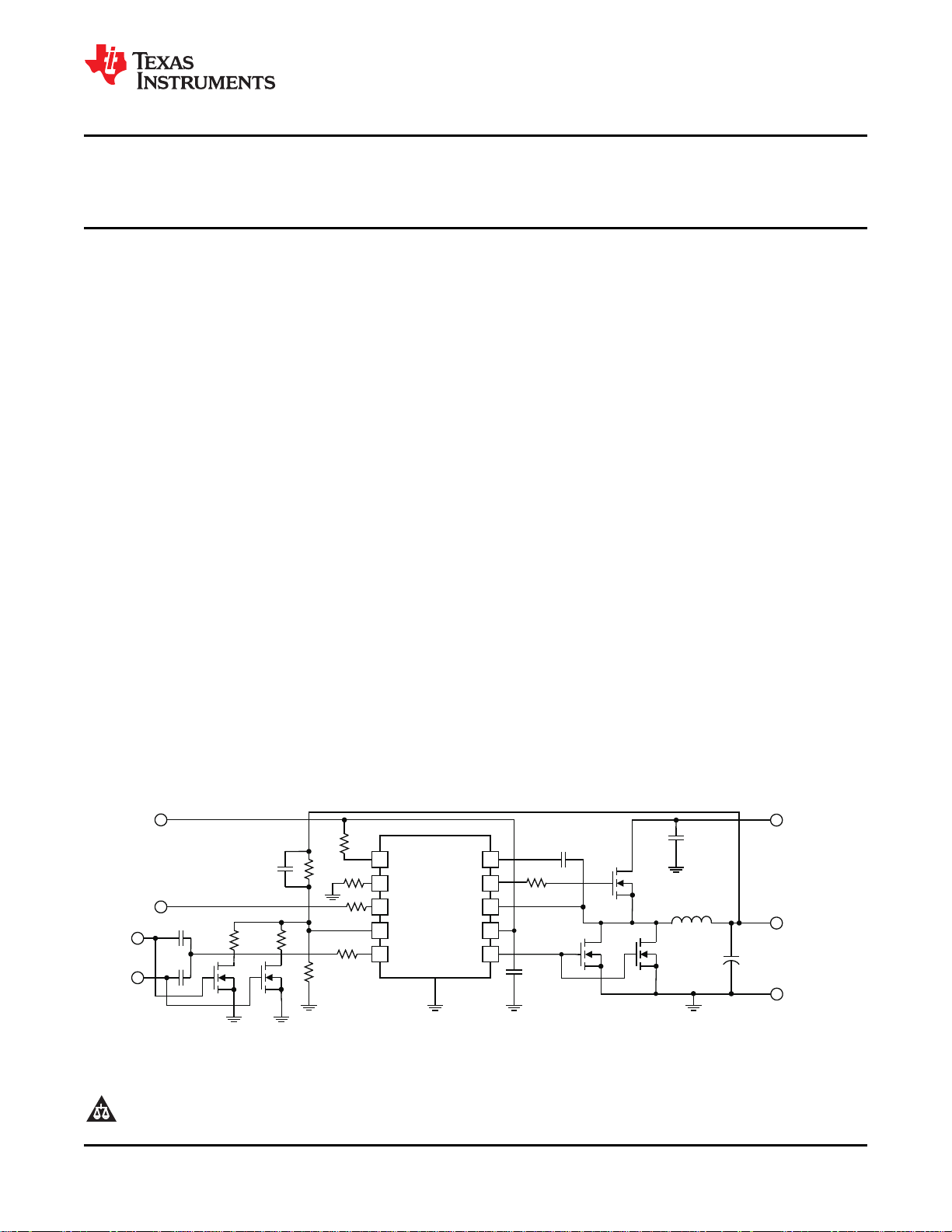
V5IN
EN
VID1
VID0
V5IN
TPS51217
V
IN
V
OUT
V _GND
OUT
www.ti.com
HIGH PERFORMANCE, SINGLE SYNCHRONOUS STEP-DOWN
CONTROLLER FOR NOTEBOOK POWER SUPPLY
Check for Samples: TPS51217
1
FEATURES
2
• Wide Input Voltage Range: 3 V to 28 V
• Output Voltage Range: 0.6 V to 2.6 V
• Wide Output Load Range: 0 to 20A+
• Built-in 0.5% 0.6 V Reference
• D-CAP™ Mode with 100-ns Load Step
Response
• Adaptive On Time Control Architecture with
Fixed 340kHz Operation
• Dynamic Output Voltage Change Capability
• 4700 ppm/°C R
• Internal 0.9-ms Voltage Servo Softstart
• Pre-Charged Start-up Capability
• Built-in Output Discharge
• Power Good Output
• Integrated Boost Switch
• Built-in OVP/UVP/OCP
• Thermal Shutdown (Non-latch)
• SON-10 (DSC) Package
Current Sensing
DS(on)
TPS51217
SLUS947B –JUNE 2009–REVISED APRIL 2012
DESCRIPTION
The TPS51217 is a small-sized single buck controller
with adaptive on-time D-CAP™ mode. The device is
suitable for low output voltage, high current, PC
system power rail and similar point-of-load (POL)
power supply in digital consumer products. A small
package with minimal pin-count saves space on the
PCB, while a dedicated EN pin and pre-set frequency
minimize design effort required for new designs. The
skip-mode at light load condition, strong gate drivers
and low-side FET R
low-loss and high efficiency, over a broad load range.
The TRAN pin provides freedom of masking
overvoltage protection, undervoltage protection and
power-good signal during the transition period of
dynamic output voltage change for modern GPU
power supply applications. The conversion input
voltage which is the high-side FET drain voltage
ranges from 3 V to 28 V and the output voltage
ranges from 0.6 V to 2.6 V. The device requires an
external 5-V supply. The TPS51217 is available in a
10-pin SON package specified from –40°C to 85°C.
current sensing supports
DS(on)
APPLICATIONS
• Notebook Computers
• I/O Supplies
• System Power Supplies
TYPICAL APPLICATION CIRCUIT
1
Please be aware that an important notice concerning availability, standard warranty, and use in critical applications of
Texas Instruments semiconductor products and disclaimers thereto appears at the end of this data sheet.
2D-CAP is a trademark of Texas Instruments.
PRODUCTION DATA information is current as of publication date.
Products conform to specifications per the terms of the Texas
Instruments standard warranty. Production processing does not
necessarily include testing of all parameters.
Copyright © 2009–2012, Texas Instruments Incorporated
TPS51217
SLUS947B –JUNE 2009–REVISED APRIL 2012
This integrated circuit can be damaged by ESD. Texas Instruments recommends that all integrated circuits be handled with
appropriate precautions. Failure to observe proper handling and installation procedures can cause damage.
ESD damage can range from subtle performance degradation to complete device failure. Precision integrated circuits may be more
susceptible to damage because very small parametric changes could cause the device not to meet its published specifications.
T
A
–40°C to 85°C Plastic SON PowerPAD
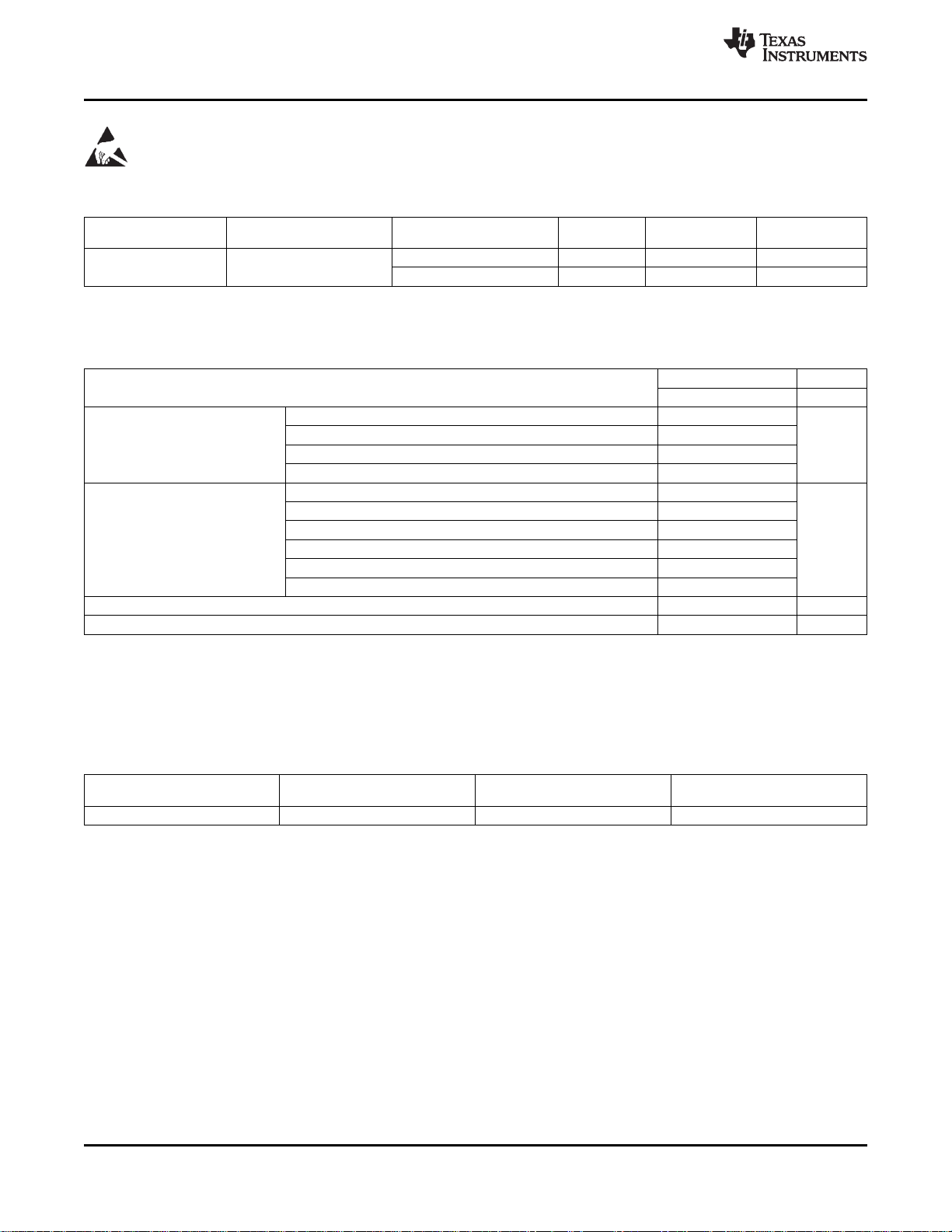
PACKAGE ORDERING DEVICE NUMBER PINS OUTPUT SUPPLY
www.ti.com
ORDERING INFORMATION
MINIMUM
QUANTITY
TPS51217DSCR 10 Tape and reel 3000
TPS51217DSCT 10 Mini reel 250
ABSOLUTE MAXIMUM RATINGS
(1)
over operating free-air temperature range (unless otherwise noted)
VALUE
MIN MAX UNIT
VBST –0.3 37
(3)
Input voltage range
Output voltage range
Junction temperature range, T
Storage temperature range, T
(2)
(2)
J
STG
VBST
SW –5 30
V5IN, EN, TRIP, VFB, TRAN –0.3 7
DRVH –5 37
(3)
DRVH
(3)
DRVH
, pulse wiidth < 20 ns –2.5 7
DRVL –0.5 7
DRVL, pulse width < 20 ns –2.5 7
PGOOD –0.3 7
–0.3 7
–0.3 7
150 °C
–55 150 °C
V
V
(1) Stresses beyond those listed under absolute maximum ratings may cause permanent damage to the device. These are stress ratings
only and functional operation of the device at these or any other conditions beyond those indicated under recommended operating
conditions is not implied. Exposure to absolute-maximum-rated conditions for extended periods may affect device reliability.
(2) All voltage values are with respect to the network ground terminal unless otherwise noted.
(3) Voltage values are with respect to the SW terminal.
DISSIPATION RATINGS
2-oz. trace and copper pad with solder.
PACKAGE
10 pin DSC
(1)
(1) Enhanced thermal conductance by thermal vias is used beneath thermal pad as shown in Land Pattern information.
TA< 25°C DERATING FACTOR TA= 85°C
POWER RATING ABOVE TA= 25°C POWER RATING
1.54 W 15 mW/°C 0.62 W
2 Submit Documentation Feedback Copyright © 2009–2012, Texas Instruments Incorporated
Product Folder Link(s) :TPS51217
TPS51217
www.ti.com
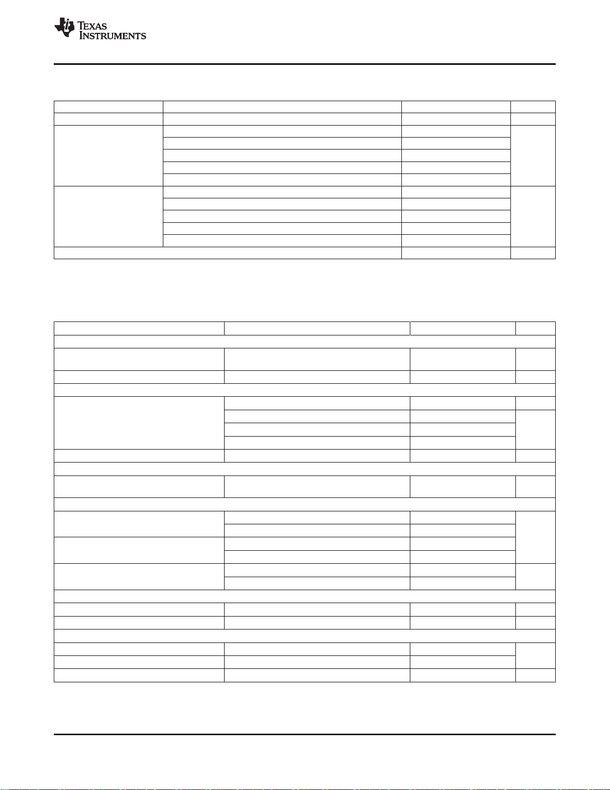
RECOMMENDED OPERATING CONDITIONS
over operating free-air temperature range (unless otherwise noted)
Supply voltage V5IN 4.5 6.5 V
VBST –0.1 34.5
SW –1 28
Input voltage range SW
Output voltage range DRVH
Operating free-air temperature, T
(1) This voltage should be applied for less than 30% of the repetitive period.
(2) Voltage values are with respect to the SW terminal.
(1)
(2)
VBST
EN, TRIP, VFB, TRAN –0.1 6.5
DRVH –1 34.5
(1)
DRVH
(2)
DRVL –0.3 6.5
PGOOD –0.1 6.5
A
ELECTRICAL CHARACTERISTICS
over recommended free-air temperature range, V5IN = 5V. (Unless otherwise noted)
PARAMETER TEST CONDITIONS MIN TYP MAX UNIT
SUPPLY CURRENT
I
(V5IN)
I
SD(V5IN)
V5IN supply current 320 500 μA
V5IN shutdown current V5IN current, TA= 25°C, No Load, V
INTERNAL REFERENCE VOLTAGE
V
(VFB)
I
(VFB)
VFB regulation voltage
VFB input current V
OUTPUT DISCHARGE
I
Dischg
Output discharge current from
SW pin
OUTPUT DRIVERS
R
(DRVH)
R
(DRVL)
t
D
DRVH resistance
DRVL resistance
Dead time ns
BOOT STRAP SWITCH
V
(FBST)
I
lkg
Forward voltage V
VBST leakage current V
DUTY AND FREQUENCY CONTROL
t
OFF(min)
t
ON(min)
f
SW
Minimum off-time TA= 25°C 150 260 400
Minimum on-time VIN= 28 V, V
Switching frequency TA= 25°C
(1) Specified by design. Not production tested.
(2) Not production tested. Test condition is VIN= 8 V, V
V5IN current, TA= 25°C, No Load,
V
= 5 V, V
(EN)
VFB voltage, CCM condition
(VFB)
= 0.63 V
= 0 V 1 μA
(EN)
(1)
TA= 25°C, skip mode 0.6000 0.6030 0.6060
TA= 0°C to 85°C, skip mode 0.5974 0.6030 0.6086 V
TA= –40°C to 85°C, skip mode 0.5960 0.6030 0.6100
= 0.63 V, TA= 25°C, skip mode 0.01 0.2 μA
(VFB)
V
= 0 V, V
(EN)
Source, I
Sink, I
(DRVH)
Source, I
Sink, I
(DRVL)
(DRVH)
(DRVL)
= 0.5 V 5 13 mA
(SW)
= –50 mA 1.5 3
= 50 mA 0.7 1.8
= –50 mA 1.0 2.2
= 50 mA 0.5 1.2
DRVH-off to DRVL-on 7 17 30
DRVL-off to DRVH-on 10 22 35
(V5IN-VBST)
(VBST)
, IF= 10 mA, TA= 25°C 0.1 0.2 V
= 34.5 V, V
OUT
(2)
= 1.1 V, I
OUT
= 28 V, TA= 25°C 0.01 1.5 μA
(SW)
= 0.6 V, TA= 25°C
= 10A using the application circuit shown in Figure 26.
OUT
(1)
SLUS947B –JUNE 2009–REVISED APRIL 2012
MIN TYP MAX UNIT
–4 28 V
–0.1 6.5
-4 34.5
–0.1 6.5 V
–40 85 °C
0.6000 V
86
312 340 368 kHz
Ω
ns
Copyright © 2009–2012, Texas Instruments Incorporated Submit Documentation Feedback 3
Product Folder Link(s) :TPS51217
TPS51217
SLUS947B –JUNE 2009–REVISED APRIL 2012
ELECTRICAL CHARACTERISTICS (continued)
over recommended free-air temperature range, V5IN = 5V. (Unless otherwise noted)
PARAMETER TEST CONDITIONS MIN TYP MAX UNIT
SOFTSTART
t
SS
POWERGOOD
V
(THPG)
I
(PG)max
t
PGDEL
LOGIC THRESHOLD AND SETTING CONDITIONS
V
(EN)
I
(EN)
V
(TRAN)
I
(TRAN)
PROTECTION: CURRENT SENSE
I
(TRIP)
V
(TRIP)
V
OCL
V
OCLN
V
AZCADJ
PROTECTION: UVP AND OVP
V
(OVP)
t
OVPDEL
V
(UVP)
t
UVPDEL
t
UVPEN
UVLO
THERMAL SHUTDOWN
T
SDN
Internal soft-start time From V
= high to V
(EN)
= 95% 0.9 ms
OUT
PG in from lower 92.5% 95% 97.5%
PG threshold PG in from higher 107.5% 110% 112.5%
PG hysteresis 2.5% 5% 7.5%
PG sink current V
= 0.5 V 3 6 mA
(PGOOD)
PG delay Delay for PG in 0.8 1 1.2 ms
EN voltage V
EN input current V
Enable 1.8
Disable 0.5
= 5V 1.0 μA
(EN)
TRAN open 1.83 1.88 1.93
TRAN voltage V
Mask PG, OVP and UVP, high side 2.03 2.08 2.13
Mask PG, OVP and UVP, low side 1.62 1.67 1.72
Hysteresis 0.05
V
= 5 V, TA= 25°C 2.5 3.8 5
TRAN input current μA
TRIP source current V
TRIP current temperature
coefficient
Current limit threshold setting
range
Current limit threshold V
Negative current limit threshold V
Adaptive zero cross adjustable
range
(TRAN)
V
= 0 V, TA= 25°C –5 –3.8 –2.5
(TRAN)
= 1V, TA= 25°C 9 10 11 μA
(TRIP)
On the basis of 25°C 4700 ppm/°C
V
(TRIP-GND)
V
(TRIP)
(TRIP)
V
(TRIP)
V
(TRIP)
(TRIP)
V
(TRIP)
voltage 0.2 3 V
= 3 V 355 375 395
= 1.6 V 185 200 215 mV
= 0.2 V 17 25 33
= 3 V –395 –375 –355
= 1.6 V –215 –200 –185 mV
= 0.2 V –33 –25 –17
Positive 3 15
Negative –15 –3
OVP trip threshold OVP detect 115% 120% 125%
OVP propagation delay time 50-mV overdrive 1 μs
Output UVP trip threshold UVP detect 65% 70% 75%
Output UVP propagation delay 0.8 1 1.2 ms
Output UVP enable delay time From Enable to UVP workable 1 1.2 1.4 ms
V5IN UVLO threshold V
Thermal shutdown threshold °C
Wake up 4.20 4.38 4.50
Shutdown 3.7 3.93 4.1
Shutdown temperature
Hysteresis
(3)
(3)
www.ti.com
mV
145
10
(3) Specified by design. Not production tested.
4 Submit Documentation Feedback Copyright © 2009–2012, Texas Instruments Incorporated
Product Folder Link(s) :TPS51217
1
2
3
4
5
10
9
8
7
6
PGOOD
TRIP
EN
VFB
TRAN
VBST
DRVH
SW
V5IN
DRVL
GND
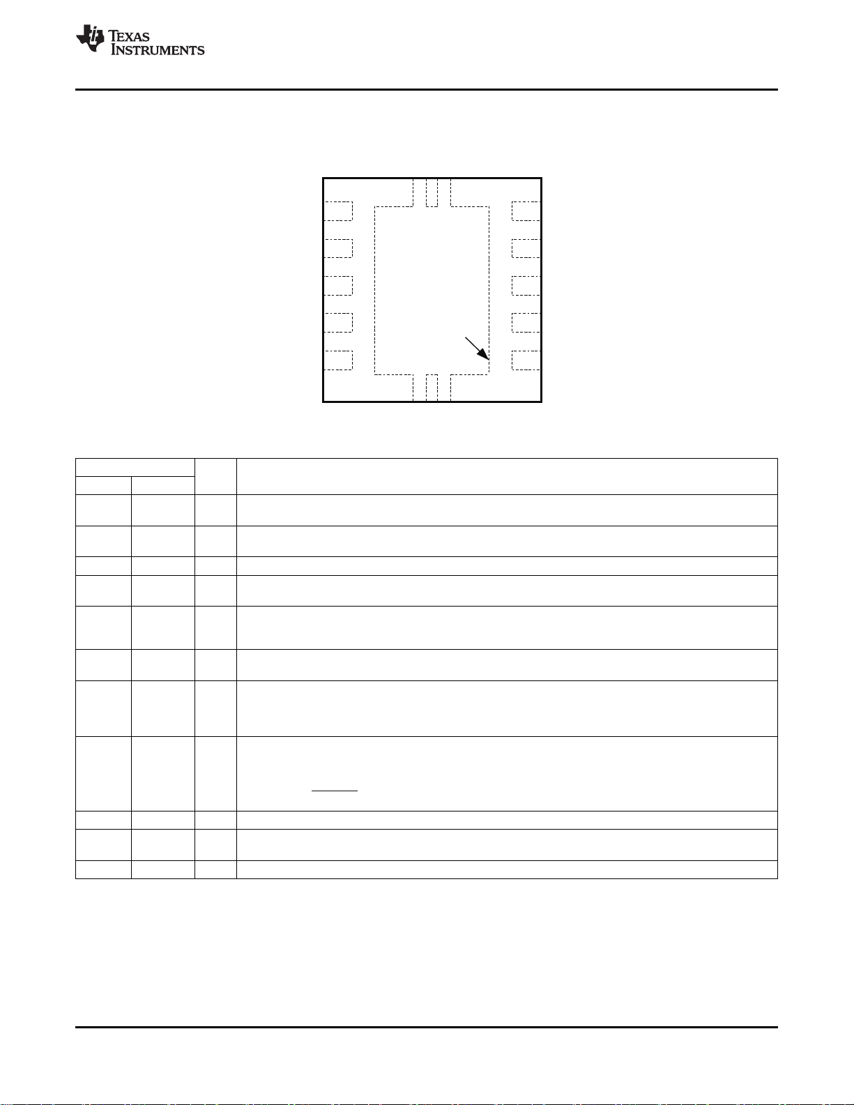
DSCPACKAGE
(TOP VIEW)
TPS51217DSC
(TRIP)
OCL
V
V
8
=
www.ti.com
SLUS947B –JUNE 2009–REVISED APRIL 2012
DEVICE INFORMATION
Thermal pad is used as an active terminal of GND.
PIN FUNCTIONS
PIN
NAME NO.
DRVH 9 O
DRVL 6 O
EN 3 I SMPS enable pin. Short to GND to disable the device.
GND I Ground
PGOOD 1 O voltage. Continuous current capability is 1 mA. PGOOD goes high 1 ms after VFB becomes within
SW 8 I
TRAN 5 I
TRIP 2 I
Thermal
Pad
I/O DESCRIPTION
High-side MOSFET driver output. The SW node referenced floating driver. The gate drive voltage is
defined by the voltage across VBST to SW node bootstrap flying capacitor
Synchronous MOSFET driver output. The GND referenced driver. The gate drive voltage is defined by
V5IN voltage.
Power Good window comparator open drain output. Pull up with resistor to 5 V or appropriate signal
specified limits. Power bad, or the terminal goes low, after a 2- μs delay.
Switch node. A high-side MOSFET gate drive return. Also used for on time generation and output
discharge.
Dynamic voltage change control. It forces CCM and masks PGOOD, OVP and UVP when this pin's status
is pulled up or pulled down. The masking is terminated 900 μs after TRAN pin voltage returns to normal.
See the DYNAMIC VOLTAGE STEP and PGOOD/OVP/UVP MASK section for a detailed description.
Leave this pin open when dynamic voltage change is not used.
OCL detection threshold setting pin. 10 μA at room temperature, 4700 ppm/°C current is sourced and set
the OCL trip voltage as follows.
(0.2 V ≤ V
(TRIP)
≤ 3 V)
TPS51217
V5IN 7 I 5 V +30% / –10% power supply input.
VBST 10 I
VFB 4 I SMPS feedback input. Connect the feedback resistor divider.
Copyright © 2009–2012, Texas Instruments Incorporated Submit Documentation Feedback 5
Supply input for high-side MOSFET driver (bootstrap terminal). Connect a flying capacitor from this pin to
the SW pin. Internally connected to V5IN via bootstrap MOSFET switch.
Product Folder Link(s) :TPS51217
+
+
-
+
VBST
DRVH
SW
DRVL
EN
VFB
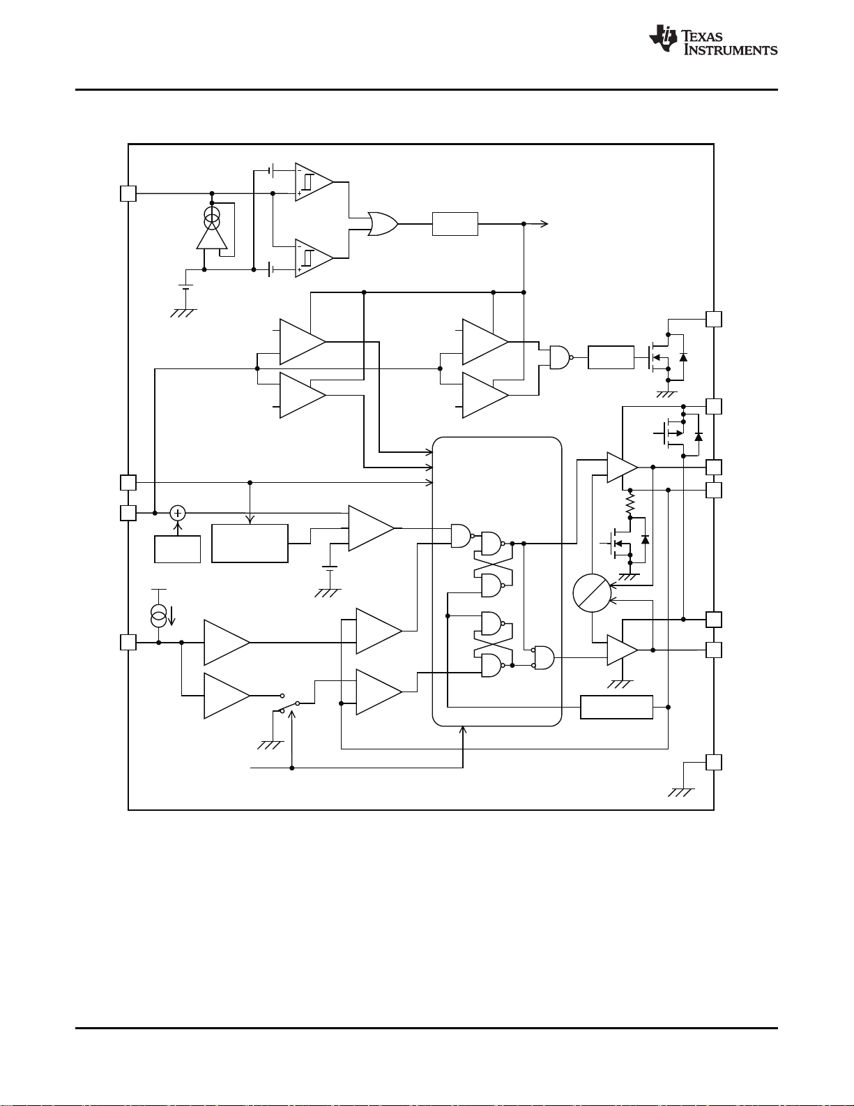
Enable /
Softstart
Control
PWM
OCP
ZC
0.6V + 10%/15%
0.6V - 5%/10%
0.6V
Delay
0.6 V - 30%
0.6 V + 20%
XCON
V5IN
Ramp
Comp
TRIP
X (-1/8)
X 1/8
TonOne-Shot
PGOOD
-
+
-
+
-
+
ControlLogic
UV
OV
Auto-skip / FCCM
10 mA
GND
-
+
-
+
FCCM
Auto-skip
TRAN
1.88 V
0.21 V/0.16 V
0.2V/0.15V
Delay
Auto-skip / FCCM
+/-3.8 mA
TPS51217
TPS51217
SLUS947B –JUNE 2009–REVISED APRIL 2012
www.ti.com
FUNCTIONAL BLOCK DIAGRAM
6 Submit Documentation Feedback Copyright © 2009–2012, Texas Instruments Incorporated
Product Folder Link(s) :TPS51217
–50
200
0
0
50 100 150
600
400
1000
800
V
(V5IN)
= 5 V
V
(EN)
= 5 V
V
(VFB)
= 0.63 V
No Load
TJ– Junction Temperature – °C
I
(V5IN)
– V5IN Supply Current – mA
–50
0
0 50 100 150
TJ– Junction Temperature – °C
4
12
8
20
16
I
SD(V5IN)
– V5IN Shutdown Current – mA
10
6
18
14
2
V
(V5IN)
= 5 V
V
(EN)
= 0 V
No Load
–50
0
0 50 100 150
TJ– Junction Temperature – °C
150
V
(OVP)
/ V
(UVP)
– OVP/UVP Trip Threshold – %
50
100
OVP
V
(V5IN)
= 5 V
UVP
–50 0 50 100 150
TJ– Junction Temperature – °C
V
(V5IN)
= 5 V
V
(TRIP)
= 1 V
0
4
12
8
20
16
I
(TRIP)
– Current Sense Current – mA
10
6
18
14
2
www.ti.com
TPS51217
SLUS947B –JUNE 2009–REVISED APRIL 2012
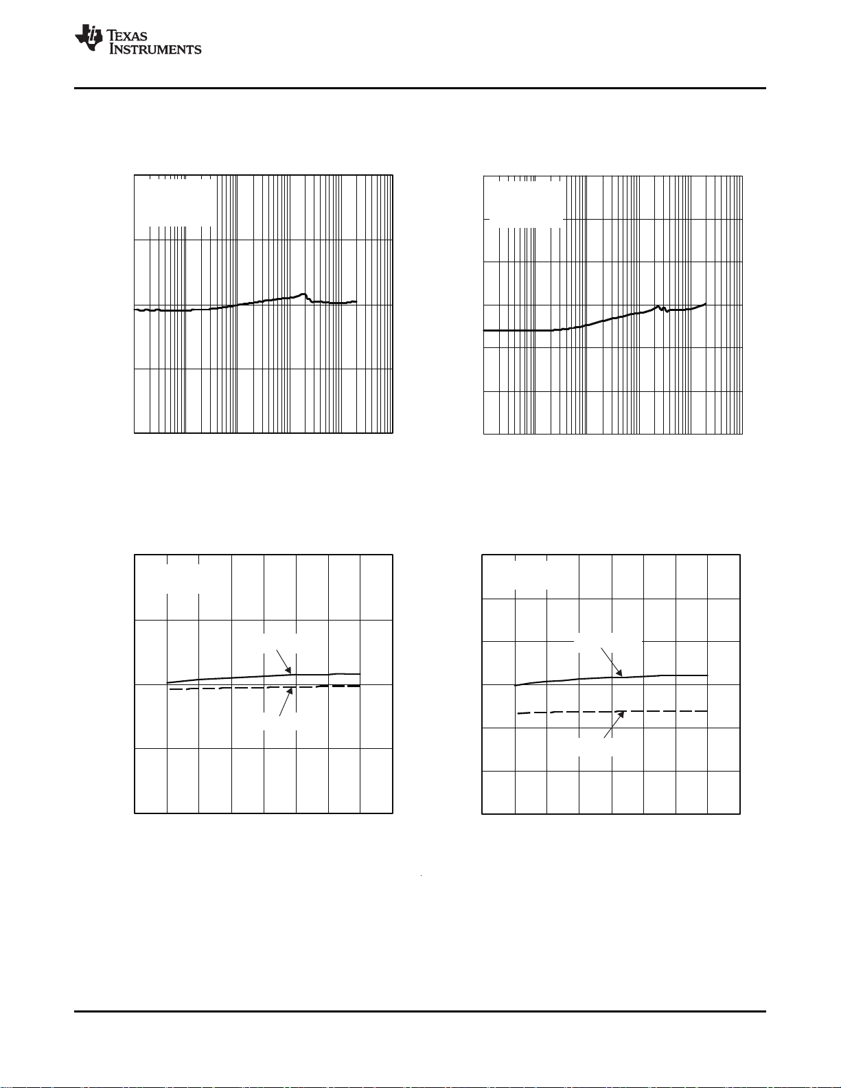
TYPICAL CHARACTERISTICS
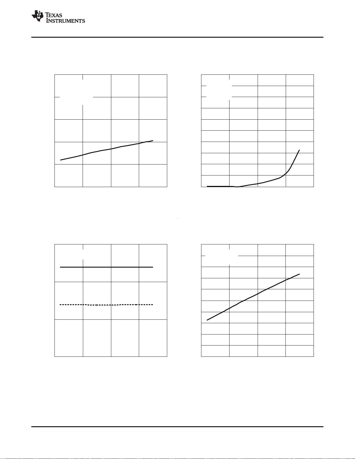
V5IN SUPPLY CURRENT V5IN SHUTDOWN CURRENT
vs vs
JUNCTION TEMPERATURE JUNCTION TEMPERATURE
Figure 1. Figure 2.
OVP/UVP THRESHOLD CURRENT SENSE CURRENT, I
vs vs
JUNCTION TEMPERATURE JUNCTION TEMPERATURE
Figure 3. Figure 4.
(TRIP)
Copyright © 2009–2012, Texas Instruments Incorporated Submit Documentation Feedback 7
Product Folder Link(s) :TPS51217
-10
-8
-6
-4
-2
0
I -TranInputCurrent- A
(TRAN)
m
-50 0 50 100 150
T -JunctionTemperature-°C
J
V =5V,
V =0V
(V5IN)
(TRAN)
-50 0 50 100 150
T -JunctionTemperature-°C
J
0
2
4
6
8
10
I -TranInputCurrent- A
(TRAN)
m
V =5V,
V =5V
(V5IN)
(TRAN)
0.1
1
10
100
1000
0.001 0.01 0.1 1 10 100
I -OutputCurrent- A
OUT
f -SwithchingFrequency-kHz
sw
Auto-Skip
V =12V,
V =1.2V
IN
OUT
6 8 10 12 14 16 18 20 22
V -InputVoltage-V
IN
200
250
300
350
400
450
500
f -SwithchingFrequency-kHz
sw
Auto-Skip
V =1.2V,
I =10 A
OUT
OUT
TPS51217
SLUS947B –JUNE 2009–REVISED APRIL 2012
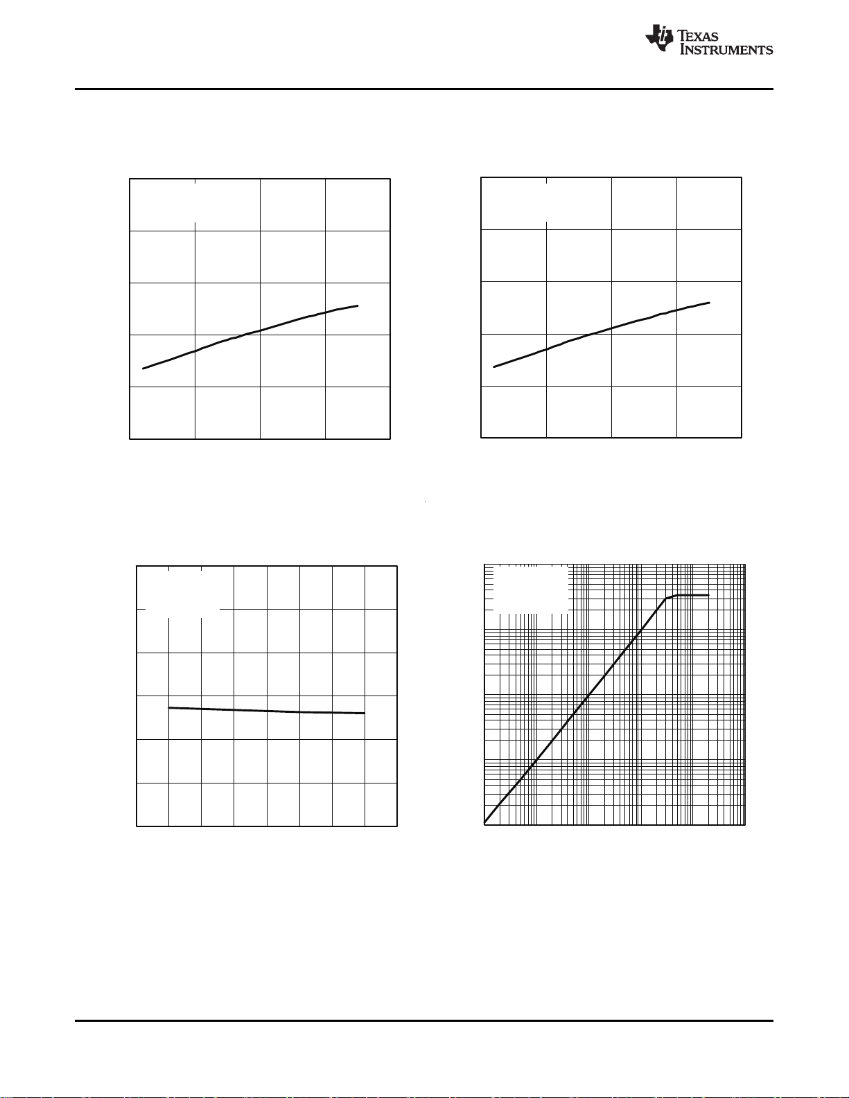
TYPICAL CHARACTERISTICS (continued)
TRAN INPUT CURRENT, I
vs vs
JUNCTION TEMPERATURE JUNCTION TEMPERATURE
(TRAN)
TRAN INPUT CURRENT, I
www.ti.com
(TRAN)
Figure 5. Figure 6.
SWITCHING FREQUENCY SWITCHING FREQUENCY
vs vs
INPUT VOLTAGE OUTPUT CURRENT
Figure 7. Figure 8.
8 Submit Documentation Feedback Copyright © 2009–2012, Texas Instruments Incorporated
Product Folder Link(s) :TPS51217
0.001 0.01 0.1 1 10 100
I -OutputCurrent- A
OUT
0.88
0.89
0.90
0.91
0.92
V -OutputVoltage-V
OUT
Auto-Skip
V =12V,
V =0.9V
IN
OUT
1.17
1.18
1.19
1.20
1.21
1.22
1.23
V -OutputVoltage-V
OUT
0.001 0.01 0.1 1 10 100
I -OutputCurrent- A
OUT
Auto-Skip
V =12V,
V =1.2V
IN
OUT
0.88
0.89
0.90
0.91
0.92
V -OutputVoltage-V
OUT
6 8 10 12 14 16 18 20 22
V -InputVoltage-V
IN
I =20 A
OUT
I =0 A
OUT
Auto-Skip
V =0.9V
OUT
1.17
1.18
1.19
1.20
1.21
1.22
1.23
I =20 A
OUT
I =0 A
OUT
V -OutputVoltage-V
OUT
6 8 10 12 14 16 18 20 22
V -InputVoltage-V
IN
Auto-Skip
V =1.2V
OUT
www.ti.com
TPS51217
SLUS947B –JUNE 2009–REVISED APRIL 2012
TYPICAL CHARACTERISTICS (continued)
0.9-V OUTPUT VOLTAGE 1.2-OUTPUT VOLTAGE
vs vs
OUTPUT CURRENT OUTPUT CURRENT
Figure 9. Figure 10.
0.9-OUTPUT VOLTAGE 1.2-V OUTPUT VOLTAGE
vs vs
INPUT VOLTAGE INPUT VOLTAGE
Figure 11. Figure 12.
Copyright © 2009–2012, Texas Instruments Incorporated Submit Documentation Feedback 9
Product Folder Link(s) :TPS51217
0.001 0.01 0.1 1 10 100
I -OutputCurrent- A
OUT
0
10
20
30
40
50
60
70
80
90
100
h -Efficiency-%
V =8V
IN
V =12V
IN
V =20V
IN
Auto-Skip
V =0.9V
OUT
0
10
20
30
40
50
60
70
80
90
100
h -Efficiency-%
0.001 0.01 0.1 1 10 100
I -OutputCurrent- A
OUT
V =8V
IN
V =12V
IN
V =20V
IN
Auto-Skip
V =1.2V
OUT
Auto-Skip
V =12V,
I =20 A
IN
OUT
EN(5V/div)
V (0.5V/div)
OUT
PGOOD(5V/div)
t-Time-500 s/divm
Auto-Skip
V =12V,
I =0 A
IN
OUT
EN(5V/div)
PGOOD(5V/div)
V (0.5V/div)
OUT
t-Time-500 s/divm
0.5Vpre-biased
TPS51217
SLUS947B –JUNE 2009–REVISED APRIL 2012
TYPICAL CHARACTERISTICS (continued)
0.9-V EFFICIENCY 1.2-V EFFICIENCY
vs vs
OUTPUT CURRENT OUTPUT CURRENT
www.ti.com
Figure 13. Figure 14.
0.9-V START-UP WAVEFORM PRE-BIASED START-UP WAVEFORM
10 Submit Documentation Feedback Copyright © 2009–2012, Texas Instruments Incorporated
Figure 15. Figure 16.
Product Folder Link(s) :TPS51217

t-Time-10ms/div
EN(5V/div)
PGOOD(5V/div)
V (0.5V/div)
OUT
Auto-Skip
V =12V,
I =0 A
IN
OUT
DRVL (5V/div)
V (50mV/div)
OUT
Auto-Skip
V =20V,
I =1 A-15 A(3A/ s)
IN
OUT
m
t-Time-100 s/divm
I (10 A/div)
IND
I (10 A/div)
OUT
VID1
(5V/div)
VID0
(5V/div)
PGOOD(5V/div)
V (0.1V/div)
OUT
t-Time-1ms/div
1.2V
0.9V
5V
Auto-Skip
V =12V,
I =0 A
IN
OUT
PGOOD(5V/div)
V (0.1V/div)
OUT
Auto-Skip
V =12V,
I =0 A
IN
OUT
t-Time-1ms/div
VID1
(5V/div)
VID0
(5V/div)
1.2V
0.9V
5V
www.ti.com
TPS51217
SLUS947B –JUNE 2009–REVISED APRIL 2012
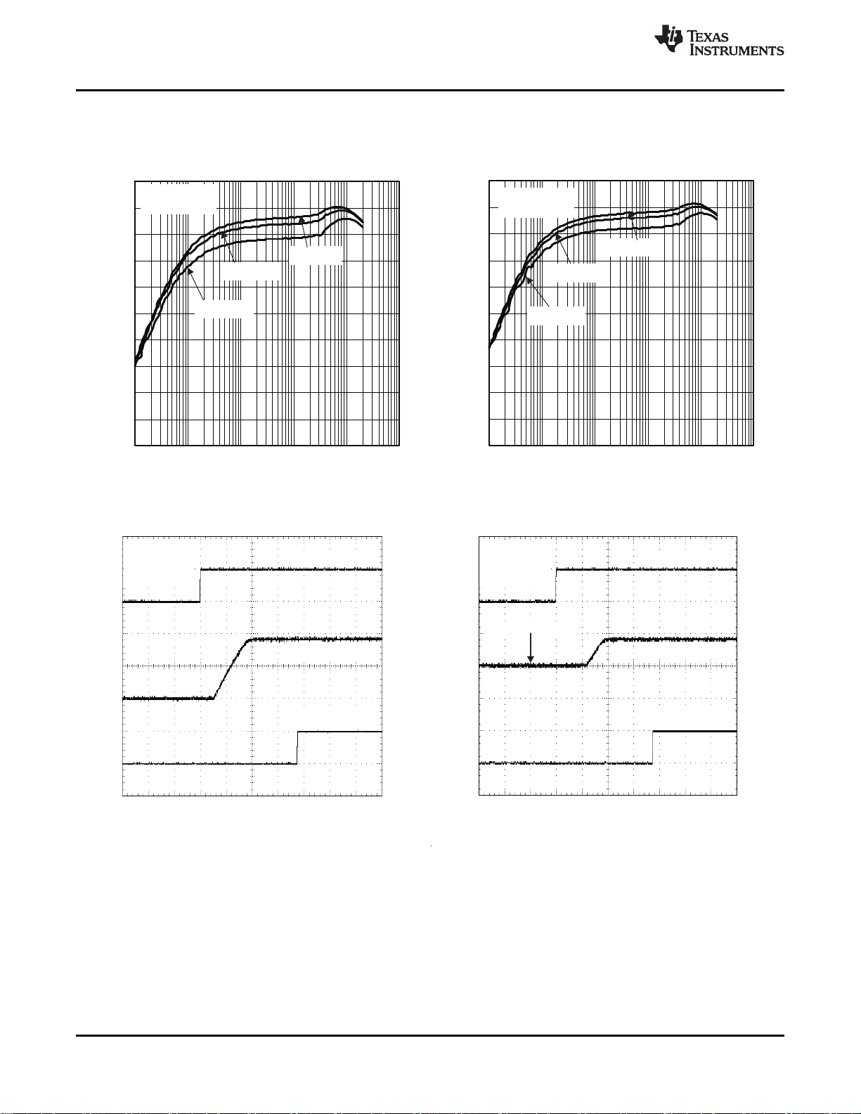
TYPICAL CHARACTERISTICS (continued)
0.9-V SOFT-STOP WAVEFORM 0.9-V LOAD TRANSIENT RESPONSE
Figure 17. Figure 18.
DYNAMIC OUTPUT VOLTAGE TRANSITION DYNAMIC OUTPUT VOLTAGE TRANSITION
Copyright © 2009–2012, Texas Instruments Incorporated Submit Documentation Feedback 11
Figure 19. Figure 20.
Product Folder Link(s) :TPS51217

TPS51217
SLUS947B –JUNE 2009–REVISED APRIL 2012
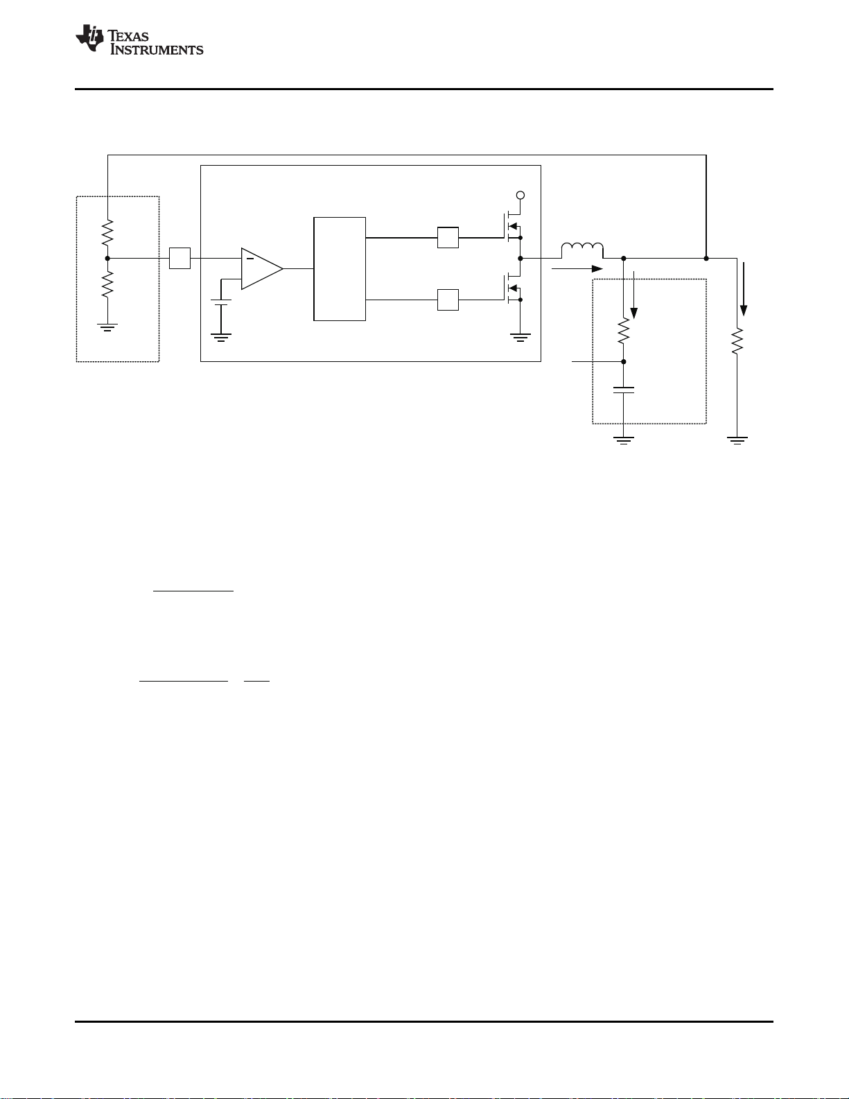
APPLICATION INFORMATION
GENERAL DESCRIPTION
The TPS51217 is a high-efficiency, single channel, synchronous buck regulator controller suitable for low output
voltage point-of-load applications in notebook computers and similar digital consumer applications. The device
features proprietary D-CAP™ mode control combined with adaptive on-time architecture. This combination is
ideal for building modern low duty ratio, ultra-fast load step response DC/DC converters. The output voltage
ranges from 0.6 V to 2.6 V. The conversion input voltage range is from 3 V to 28 V. The D-CAP™ mode uses the
ESR of the output capacitor(s) to sense current information. An advantage of this control scheme is that it does
not require an external phase compensation network, helping the designer with ease-of-use and realizing low
external component count configuration. Adaptive on-time control tracks the preset switching frequency over a
wide range of input and output voltages, while it increases the switching frequency at step-up of load.
The strong gate drivers of the TPS51217 allow low R
FETs for high current applications.
DS(on)
ENABLE AND SOFT START
When the EN pin voltage rises above the enable threshold, (typically 1.2 V) the controller enters its start-up
sequence. The first 250 μs is a standby phase. Switching is inhibited during this phase. In the second phase,
internal DAC starts ramping up the reference voltage from 0 V to 0.6 V. This ramping time is 650 μs. Smooth and
constant ramp up of the output voltage is maintained during start up regardless of load current. Connect a 1-kΩ
resistor in series with the EN pin to provide protection.
ADAPTIVE ON-TIME D-CAP™ CONTROL
TPS51217 does not have a dedicated oscillator that determines switching frequency. However, the device runs
with pseudo-constant frequency by feed-forwarding the input and output voltages into its on-time one-shot timer.
The adaptive on-time control adjusts the on-time to be inversely proportional to the input voltage and proportional
to the output voltage (tON∝ V
conditions over wide input voltage range.
The off-time is modulated by a PWM comparator. The VFB node voltage (the mid point of resistor divider) is
compared to the internal 0.6-V reference voltage added with a ramp signal. When both signals match, the PWM
comparator asserts the set signal to terminate the off-time (turn off the low-side MOSFET and turn on high-side
MOSFET). The set signal becomes valid if the inductor current level is below OCP threshold, otherwise the offtime is extended until the current level to become below the threshold.
/ VIN). This makes the switching frequency fairly constant in steady state
OUT
www.ti.com
12 Submit Documentation Feedback Copyright © 2009–2012, Texas Instruments Incorporated
Product Folder Link(s) :TPS51217
R1
R2
Voltage Divider
+
V
FB
+
0.6 V
PWM
Control
Logic
and
Driver
V
IN
L
ESR
C
O
V
C
R
L
I
IND
I
OUT
UDG-09063
I
C
Switching Modulator
Output
Capacitor
DRVH
DRVL
V
OUT
O
1
H(s)
s ESR C
=
´ ´
f
SW
0
O
1
f
2 ESR C 4
= £
p´ ´
TPS51217
www.ti.com
SMALL SIGNAL MODEL
From small-signal loop analysis, a buck converter using D-CAP™ mode can be simplified as shown in Figure 21.
SLUS947B –JUNE 2009–REVISED APRIL 2012
Figure 21. Simplified Modulator Model
The output voltage is compared with internal reference voltage (ramp signal is ignored here for simplicity). The
PWM comparator determines the timing to turn on the high-side MOSFET. The gain and speed of the
comparator can be assumed high enough to keep the voltage at the beginning of each on cycle substantially
constant.
(1)
For loop stability, the 0-dB frequency, ƒ0, defined in Equation 2 need to be lower than 1/4 of the switching
frequency.
(2)
According to Equation 2, the loop stability of D-CAP™ mode modulator is mainly determined by the capacitor's
chemistry. For example, specialty polymer capacitors (SP-CAP) have COon the order of several 100 μF and
ESR in range of 10 mΩ. These makes f0on the order of 100 kHz or less and the loop is stable. However,
ceramic capacitors have an ƒ0of more than 700 kHz, which is not suitable for this modulator.
RAMP SIGNAL
The TPS51217 adds a ramp signal to the 0.6-V reference in order to improve its jitter performance. As described
in the previous section, the feedback voltage is compared with the reference information to keep the output
voltage in regulation. By adding a small ramp signal to the reference, the S/N ratio at the onset of a new
switching cycle is improved. Therefore the operation becomes less jittery and more stable. The ramp signal is
controlled to start with –6 mV at the beginning of ON-cycle and becomes 0 mV at the end of OFF-cycle in
continuous conduction steady state.
Copyright © 2009–2012, Texas Instruments Incorporated Submit Documentation Feedback 13
Product Folder Link(s) :TPS51217

( )
f
IN OUT OUT
O LL
SW IN
(V V ) V
1
I
2 L V
- ´
= ´
´ ´
TPS51217
SLUS947B –JUNE 2009–REVISED APRIL 2012
LIGHT LOAD CONDITION IN AUTO-SKIP OPERATION
The TPS51217 automatically reduces switching frequency at light load conditions to maintain high efficiency. As
the output current decreases from heavy load condition, the inductor current is also reduced and eventually
comes to the point that its rippled valley touches zero level, which is the boundary between continuous
conduction and discontinuous conduction modes. The rectifying MOSFET is turned off when this zero inductor
current is detected. As the load current further decreases, the converter runs in to discontinuous conduction
mode. The on-time is kept almost the same as it was in the continuous conduction mode so that it takes longer
time to discharge the output capacitor with smaller load current to the level of the reference voltage. The
transition point to the light load operation I
(i.e., the threshold between continuous and discontinuous
O(LL)
conduction mode) can be calculated in Equation 3.
where
• fSWis the PWM switching frequency (340 kHz) (3)
Switching frequency versus output current in the light load condition is a function of L, VINand V
decreases almost proportional to the output current from the I
at I
O(LL)
/5.
given in Equation 3. For example, it is 68 kHz
O(LL)
ADAPTIVE ZERO CROSSING
The TPS51217 has an adaptive zero crossing circuit which performs optimization of the zero inductor current
detection at skip mode operation. This function pursues ideal low-side MOSFET turning off timing and
compensates inherent offset voltage of the ZC comparator and delay time of the ZC detection circuit. It prevents
SW-node swing-up caused by too late detection and minimizes diode conduction period caused by too early
detection. As a result, better light load efficiency is delivered.
www.ti.com
, but it
OUT
OUTPUT DISCHARGE CONTROL
When EN is low, the TPS51217 discharges the output capacitor using internal MOSFET connected between SW
and GND while high-side and low-side MOSFETs are kept off. The current capability of this MOSFET is limited to
discharge slowly.
LOW-SIDE DRIVER
The low-side driver is designed to drive high current low R
represented by its internal resistance, which are 1.0Ω for V5IN to DRVL and 0.5Ω for DRVL to GND. A dead time
to prevent shoot through is internally generated between high-side MOSFET off to low-side MOSFET on, and
low-side MOSFET off to high-side MOSFET on. 5-V bias voltage is delivered from V5IN supply. The
instantaneous drive current is supplied by an input capacitor connected between V5IN and GND. The average
drive current is equal to the gate charge at Vgs=5V times switching frequency. This gate drive current as well as
the high-side gate drive current times 5V makes the driving power which need to be dissipated from TPS51217
package.
N-channel MOSFET(s). The drive capability is
DS(on)
HIGH-SIDE DRIVER
The high-side driver is designed to drive high current, low R
floating driver, 5 V of bias voltage is delivered from V5IN supply. The average drive current is also equal to the
gate charge at Vgs = 5V times switching frequency. The instantaneous drive current is supplied by the flying
capacitor between VBST and SW pins. The drive capability is represented by its internal resistance, which are
1.5 Ω for VBST to DRVH and 0.7 Ω for DRVH to SW.
N-channel MOSFET(s). When configured as a
DS(on)
14 Submit Documentation Feedback Copyright © 2009–2012, Texas Instruments Incorporated
Product Folder Link(s) :TPS51217

( )
IND ripple
(TRIP) (TRIP)
IN OUT OUT
OCP
DS(on) DS(on) SW IN
I
V V
(V V ) V
1
I
8 R 2 8 R 2 L V
æ ö
- ´
ç ÷
= + = + ´
ç ÷
´ ´ ´ ´
è ø
f
TPS51217
www.ti.com
POWER-GOOD
The TPS51217 has powergood output that indicates high when switcher output is within the target. The
powergood function is activated after soft-start has finished. If the output voltage becomes within +10%/–5% of
the target value, internal comparators detect power-good state and the power-good signal becomes high after a
1-ms internal delay. If the output voltage goes outside of +15%/–10% of the target value, the powergood signal
becomes low after a 2-μs internal delay. The powergood output is an open-drain output and must be pulled up
externally.
CURRENT SENSE AND OVERCURRENT PROTECTION
TPS51217 has cycle-by-cycle overcurrent limiting control. The inductor current is monitored during the OFF state
and the controller keeps the OFF state during the inductor current is larger than the overcurrent trip level. To
provide both good accuracy and cost effective solution, the TPS51217 supports temperature compensated
MOSFET R
R
. The TRIP terminal sources I
(TRIP)
is set to the OCL trip voltage V
internally.
V
(mV) = R
(TRIP)
The inductor current is monitored by the voltage between GND pad and SW pin so that the SW pin should be
connected to the drain terminal of the low-side MOSFET properly. I
compensate the temperature dependency of the R
that GND should be connected to the proper current sensing device, i.e. the source terminal of the low-side
MOSFET.
As the comparison is done during the OFF state, V
current at overcurrent threshold, I
sensing. The TRIP pin should be connected to GND through the trip voltage setting resistor,
DS(on)
(TRIP)
(kΩ) × I
(TRIP)
(μA) (4) (4)
(TRIP)
OCP
current, which is 10μA typically at room temperature, and the trip level
(TRIP)
as shown in Equation 4. Note that V
. GND is used as the positive current sensing node so
DS(on)
sets valley level of the inductor current. Thus, the load
(TRIP)
(TRIP)
, can be calculated in Equation 5
SLUS947B –JUNE 2009–REVISED APRIL 2012
is limited up to approximately 3 V
(TRIP)
has 4700ppm/°C temperature slope to
(5)
In an overcurrent condition, the current to the load exceeds the current to the output capacitor thus the output
voltage tends to fall down. Eventually, it crosses the undervoltage protection threshold and shuts down the
controller.
When the device is operating in the forced continuous conduction mode, the negative current limit (NCL) protects
the external FET from carrying too much current. The NCL detect threshold is set as the same absolute value as
positive OCL but negative polarity. Note that the forced continuous conduction mode appears only during the
Dynamic Voltage Step operation, and the threshold still represents the valley value of the inductor current.
OVER/UNDER VOLTAGE PROTECTION
TPS51217 monitors a resistor divided feedback voltage to detect over and undervoltage. When the feedback
voltage becomes higher than 120% of the target voltage, the OVP comparator output goes high and the circuit
latches as the high-side MOSFET driver OFF and the low-side MOSFET driver ON.
When the feedback voltage becomes lower than 70% of the target voltage, the UVP comparator output goes
high and an internal UVP delay counter begins counting. After a 1-ms delay, TPS51217 latches OFF both highside and low-side MOSFETs drivers. This function is enabled after 1.2 ms following EN has become high.
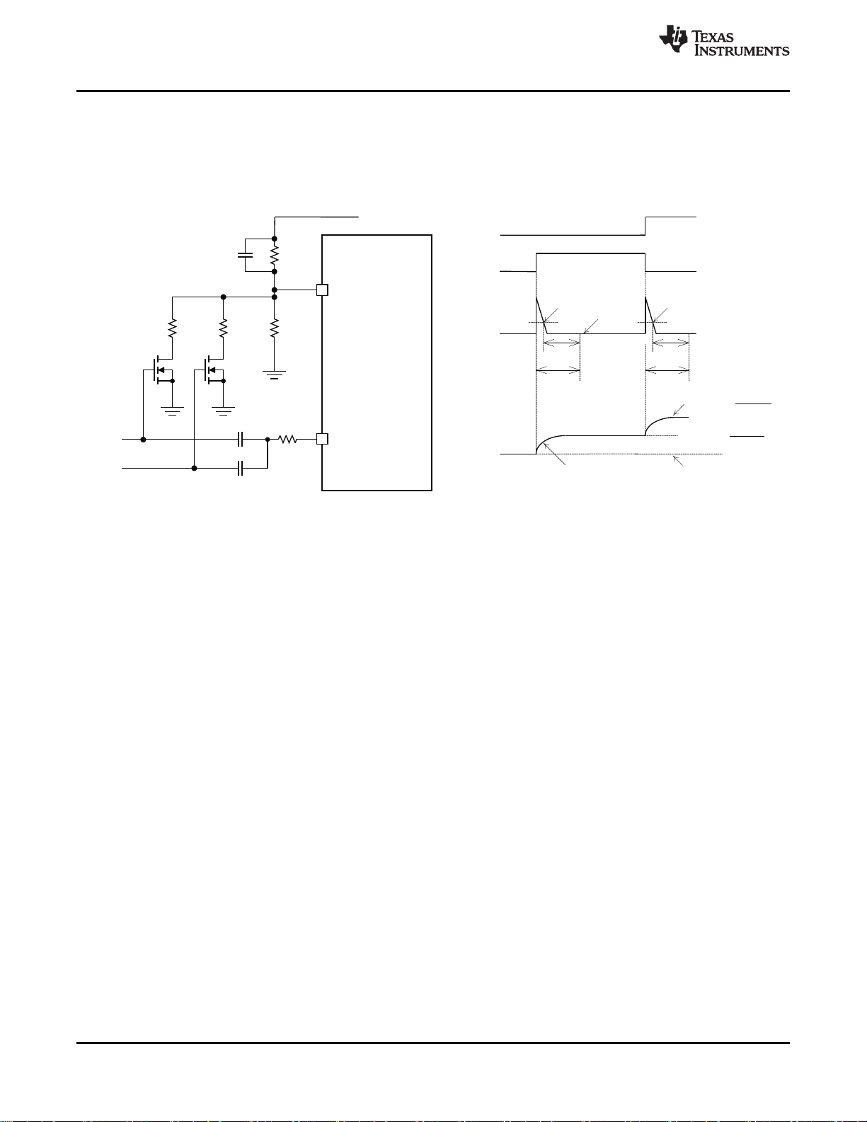
DYNAMIC VOLTAGE STEP and PGOOD/OVP/UVP MASK
Output voltage of switcher can be dynamically step-up or step-down by controlling bottom resistance of the
output voltage divider. The simplest way is to add a MOSFET switch plus a resistor in parallel with the bottom
resistor. When the MOSFET switch is turned on, the VFB voltage is immediately dropped and comes back
equivalent to the internal reference voltage as the output voltage climbs up to match the new target. If the voltage
step is large, it may cause PGOOD state into 'bad' and also may hit UVP. In the case of voltage step-down, the
same PGOOD bad and OVP hit may happen. TRAN pin helps masking PGOOD, UVP and OVP during the
voltage transition. Combination of weighted capacitances C2 and C3 detect transition of VIDx (Figure 22).
Masking of PGOOD, OVP and UVP start when the TRAN pin voltage goes outside of its window comparator
threshold. At this time, TRAN pin also starts sink or source current. 900μsec after TRAN pin voltage recovers
Copyright © 2009–2012, Texas Instruments Incorporated Submit Documentation Feedback 15
Product Folder Link(s) :TPS51217
VFB
TRAN
Vout
VID1
TPS51217
DisablePGOOD
andOVP/UVP
DisablePGOOD
andOVP/UVP
V
OUT
TRAN
VID0
)
3//2
1
1(6.0
RR
R
V +´
R5
VID0
R1
R2R3R4
C2
C3
)2/11(6.0 RRV +´
)
4//2
1
1(6.0
RR
R
V +´
VID1
C1
900 ms
900 ms
1.88 V
2.03 V
11 CR ´=t
2.03 V
322 CC ´=
TPS51217
SLUS947B –JUNE 2009–REVISED APRIL 2012
within the threshold window, PGOOD, OVP and UVP are released from masking. The TRAN pin operation is
useful for graphics power applications such that switcher output voltage needs to be changed dynamically. At the
transition of output voltage, inductor current has a chance to hit over current limit (OCL) to quickly charge the
output capacitor, which may cause output voltage undershoot or overshoot. Capacitance C1 in parallel with the
top resistor slows down transition slew rate and prevent from hitting OCL. Time constant of the transition is
R1 × C1. From 3.3 V to 5 V is recommended for VIDx input amplitude.
www.ti.com
Figure 22. Dynamic Voltage Step Application
UVLO PROTECTION
TPS51217 has V5IN undervoltage lockout protection (UVLO). When the V5IN voltage is lower than UVLO
threshold voltage, the switch mode power supply shuts off. This is non-latch protection.
THERMAL SHUTDOWN
TPS51217 monitors the die temperature. If the temperature exceeds the threshold value (typically 145°C), the
TPS51217 is shut off. This is non-latch protection.
16 Submit Documentation Feedback Copyright © 2009–2012, Texas Instruments Incorporated
Product Folder Link(s) :TPS51217

( )
(
)
( ) ( )
( )
(
)
( )
OUT OUT OUT OUT
IN max IN max
IND(ripple) SW SW
IN max OUT max IN max
V V V V V V
1 3
L
I V I V
- ´ - ´
= ´ = ´
´ ´f f
( )
(
)
( )
OUT OUT
IN max
(TRIP)
IND(peak)
DS(on) SW
IN max
V - V V
V
1
I
8 R L V
´
= + ´
× × f
( )
OUT
SW SW
IND(ripple)
V 10 mV 1-D
10[mV] L ƒ L ƒ
ESR = = = [Ω]
0.6[V] I 0.6[V] 60
´ ´
é ù
´ ´ ´
ë û
´
t
SW
t – Time
0
V
(VFB)
– Feedback Voltage – mV
10
tSWx (1-D)
V
RIPPLE(FB)
TPS51217
www.ti.com
EXTERNAL COMPONENTS SELECTION
Selecting external components is simple in D-CAP™ mode.
1. Choose the inductor.
The inductance value should be determined to give the ripple current of approximately 1/4 to 1/2 of maximum
output current. Larger ripple current increases output ripple voltage and improves S/N ratio and helps stable
operation.
The inductor also needs to have low DCR to achieve good efficiency, as well as enough room above peak
inductor current before saturation. The peak inductor current can be estimated in Equation 7.
2. Choose the output capacitor(s).
Organic semiconductor capacitor(s) or specialty polymer capacitor(s) are recommended. For loop stability,
capacitance and ESR should satisfy Equation 2. For jitter performance, Equation 8 is a good starting point to
determine ESR.
SLUS947B –JUNE 2009–REVISED APRIL 2012
(6)
(7)
where
• D is the duty ratio
• the output ripple down slope rate is 10 mV/tSWin terms of VFB terminal voltage as shown in Figure 23
• tSWis the switching period (8)
Figure 23. Ripple Voltage Down Slope
Copyright © 2009–2012, Texas Instruments Incorporated Submit Documentation Feedback 17
Product Folder Link(s) :TPS51217

IND(ripple)
OUT
I ESR
V 0.6
2
R1 = R2
0.6
´
æ ö
- -
ç ÷
ç ÷
è ø
´
UDG-090 66
TPS51217
DRVL
4
VIN
10 mF
VFB
V5IN
V
OUT
2
TRIP
# 2
# 1
# 3
5
6
Therm al Pad
GND
1 Fm
TPS51217
SLUS947B –JUNE 2009–REVISED APRIL 2012
3. Determine the value of R1 and R2.
The output voltage is programmed by the voltage-divider resistor, R1 and R2, shown in Figure 21. R1 is
connected between the VFB pin and the output, and R2 is connected between the VFB pin and GND. Typical
designs begin with the selection of an R2 value between 10 kΩ and 20 kΩ. Determine R1 using Equation 9.
LAYOUT CONSIDERATIONS
www.ti.com
(9)
Figure 24. Ground System of DC/DC Converter Using the TPS51217
Certain points must be considered before starting a layout work using the TPS51217.
• Inductor, VINcapacitor(s), V
on one side of the PCB (solder side). Other small signal components should be placed on another side
(component side). At least one inner plane should be inserted, connected to ground, in order to shield and
isolate the small signal traces from noisy power lines.
• All sensitive analog traces and components such as VFB, PGOOD, TRIP and TRAN should be placed away
from high-voltage switching nodes such as SW, DRVL, DRVH or VBST to avoid coupling. Use internal
layer(s) as ground plane(s) and shield feedback trace from power traces and components.
• The DC/DC converter has several high-current loops. The area of these loops should be minimized in order to
suppress generating switching noise.
– The most important loop to minimize the area of is the path from the VINcapacitor(s) through the high and
low-side MOSFETs, and back to the capacitor(s) through ground. Connect the negative node of the V
capacitor(s) and the source of the low-side MOSFET at ground as close as possible. (See loop #1 of
Figure 24)
– The second important loop is the path from the low-side MOSFET through inductor and V
and back to source of the low-side MOSFET through ground. Connect source of the low-side MOSFET
and negative node of V
– The third important loop is of gate driving system for the low-side MOSFET. To turn on the low-side
MOSFET, high current flows from V5IN capacitor through gate driver and the low-side MOSFET, and back
to negative node of the capacitor through ground. To turn off the low-side MOSFET, high current flows
from gate of the low-side MOSFET through the gate driver and GND pad of the device, and back to
source of the low-side MOSFET through ground. Connect negative node of V5IN capacitor, source of the
low-side MOSFET and GND pad of the device at ground as close as possible. (See loop #3 of Figure 24)
18 Submit Documentation Feedback Copyright © 2009–2012, Texas Instruments Incorporated
capacitor(s) and MOSFETs are the power components and should be placed
OUT
capacitor(s) at ground as close as possible. (See loop #2 of Figure 24)
OUT
Product Folder Link(s) :TPS51217
OUT
IN
capacitor(s),

UDG-09067
TPS51217
Thermal Pad
DRVL
4 5
VIN
10 mF
VFB
V5IN
6
V
OUT
2
TRIP
0.1 mF
100 W
VTT_SENSE
VSS_SENSE
GND
1 Fm
www.ti.com
TPS51217
SLUS947B –JUNE 2009–REVISED APRIL 2012
• Since the TPS51217 controls output voltage referring to voltage across V
the voltage divider should be connected to the positive node of V
OUT
bottom side resistor and GND pad of the device should be connected to the negative node of V
capacitor, the top-side resistor of
OUT
capacitor. In a same manner both
capacitor.
OUT
The trace from these resistors to the VFB pin should be short and thin. Place on the component side and
avoid via(s) between these resistors and the device.
• Connect the overcurrent setting resistors from TRIP pin to ground and make the connections as close as
possible to the device. The trace from TRIP pin to resistor and from resistor to ground should avoid coupling
to a high-voltage switching node.
• Connections from gate drivers to the respective gate of the high-side or the low-side MOSFET should be as
short as possible to reduce stray inductance. Use 0.65 mm (25 mils) or wider trace and via(s) of at least
0.5 mm (20 mils) diameter along this trace.
• The PCB trace defined as switch node, which connects to source of high-side MOSFET, drain of low-side
MOSFET and high-voltage side of the inductor, should be as short and wide as possible.
LAYOUT CONSIDERATIONS TO REMOTE SENSING
Figure 25. Remote Sensing of Output Voltage Using the TPS51217
• Make a Kelvin connection to the load device.
• Run the feedback signals as a differential pair to the device. The distance of these parallel pair should be as
short as possible.
• Run the lines in a quiet layer. Isolate them from noisy signals by a voltage or ground plane.
Copyright © 2009–2012, Texas Instruments Incorporated Submit Documentation Feedback 19
Product Folder Link(s) :TPS51217

V5IN
4.5 V
to
6.5 V
TRAN
VFB
EN
TRIP
DRVL
V5IN
SW
DRVH
GND
PGOOD
VBST
V
IN
8V to20V
VOUT_GND
VOUT
0.9 Vto 1.2 V
18 A
TPS51217
EN
1
3
4
5
2
6
10
7
8
9
VID1
VID0
R2
20.5 kW
R1
10 kW
R8
30 kW
C4
0.1 mF
C6
10 mFx 4
Q1
FDMS8680
Q2
FDMS8670AS
L1
0.45 mH
C7
330 mFx 4
R3
60.4 kW
R4
30 kW
C2
100 pF
C3
51 pF
Q4
Q5
R5
1 kW
R7
1 kW
C1
4.7 nF
Q3
FDMS8670AS
C5
1 mF
R6
100 kW
3.3 W
R9
TPS51217
SLUS947B –JUNE 2009–REVISED APRIL 2012
TPS51217 APPLICATION CIRCUIT
Figure 26. 0.9-V to 1.2-V/18A Auto-skip mode
Table 1. 0.9-V to 1.2-V/18A Application List of Materials
REFERENCE
DESIGNATOR
C6 1 4 × 10 μF, 25 V Taiyo Yuden TMK325BJ106MM
C7 1 4 × 330 μF, 2 V, 12 mΩ Panasonic EEFCX0D331XR
L1 1 0.45 μH, 25 A, 1.1 mΩ Panasonic ETQP4LR45XFC
Q1 1 30 V, 35 A, 8.5 mΩ Fairchild FDMS8680
Q2, Q3 2 30 V, 42 A, 3.5 mΩ Fairchild FDMS8670AS
QTY SPECIFICATION MANUFACTURER PART NUMBER
www.ti.com
20 Submit Documentation Feedback Copyright © 2009–2012, Texas Instruments Incorporated
Product Folder Link(s) :TPS51217

TPS51217
www.ti.com
REVISION HISTORY
Changes from Original (June 2009) to Revision A Page
• Added text - Connect a 1-kΩ resistor in series with the EN pin to provide protection. To the ENABLE AND SOFT
START section. ................................................................................................................................................................... 12
Changes from Revision A (August 2009) to Revision B Page
• Added DRVH specification to the ABSOLUTE MAXIMUM RATINGS table for pulse width < 20 ns ................................... 2
• Added DRVL specification to the ABSOLUTE MAXIMUM RATINGS table for pulse width < 20 ns .................................... 2
SLUS947B –JUNE 2009–REVISED APRIL 2012
Copyright © 2009–2012, Texas Instruments Incorporated Submit Documentation Feedback 21
Product Folder Link(s) :TPS51217

PACKAGE OPTION ADDENDUM
www.ti.com
19-Jun-2015
PACKAGING INFORMATION
Orderable Device Status
TPS51217DSCR ACTIVE WSON DSC 10 3000 Green (RoHS
TPS51217DSCT ACTIVE WSON DSC 10 250 Green (RoHS
(1)
The marketing status values are defined as follows:
ACTIVE: Product device recommended for new designs.
LIFEBUY: TI has announced that the device will be discontinued, and a lifetime-buy period is in effect.
NRND: Not recommended for new designs. Device is in production to support existing customers, but TI does not recommend using this part in a new design.
PREVIEW: Device has been announced but is not in production. Samples may or may not be available.
OBSOLETE: TI has discontinued the production of the device.
Package Type Package
(1)
Drawing
Pins Package
Qty
Eco Plan
(2)
& no Sb/Br)
& no Sb/Br)
Lead/Ball Finish
(6)
CU NIPDAU |
CU NIPDAUAG
CU NIPDAU |
CU NIPDAUAG
MSL Peak Temp
(3)
Level-2-260C-1 YEAR -40 to 85 PIYI
Level-2-260C-1 YEAR -40 to 85 PIYI
Op Temp (°C) Device Marking
(4/5)
(2)
Eco Plan - The planned eco-friendly classification: Pb-Free (RoHS), Pb-Free (RoHS Exempt), or Green (RoHS & no Sb/Br) - please check http://www.ti.com/productcontent for the latest availability
information and additional product content details.
TBD: The Pb-Free/Green conversion plan has not been defined.
Pb-Free (RoHS): TI's terms "Lead-Free" or "Pb-Free" mean semiconductor products that are compatible with the current RoHS requirements for all 6 substances, including the requirement that
lead not exceed 0.1% by weight in homogeneous materials. Where designed to be soldered at high temperatures, TI Pb-Free products are suitable for use in specified lead-free processes.
Pb-Free (RoHS Exempt): This component has a RoHS exemption for either 1) lead-based flip-chip solder bumps used between the die and package, or 2) lead-based die adhesive used between
the die and leadframe. The component is otherwise considered Pb-Free (RoHS compatible) as defined above.
Green (RoHS & no Sb/Br): TI defines "Green" to mean Pb-Free (RoHS compatible), and free of Bromine (Br) and Antimony (Sb) based flame retardants (Br or Sb do not exceed 0.1% by weight
in homogeneous material)
(3)
MSL, Peak Temp. - The Moisture Sensitivity Level rating according to the JEDEC industry standard classifications, and peak solder temperature.
(4)
There may be additional marking, which relates to the logo, the lot trace code information, or the environmental category on the device.
(5)
Multiple Device Markings will be inside parentheses. Only one Device Marking contained in parentheses and separated by a "~" will appear on a device. If a line is indented then it is a continuation
of the previous line and the two combined represent the entire Device Marking for that device.
(6)
Lead/Ball Finish - Orderable Devices may have multiple material finish options. Finish options are separated by a vertical ruled line. Lead/Ball Finish values may wrap to two lines if the finish
value exceeds the maximum column width.
Important Information and Disclaimer:The information provided on this page represents TI's knowledge and belief as of the date that it is provided. TI bases its knowledge and belief on information
provided by third parties, and makes no representation or warranty as to the accuracy of such information. Efforts are underway to better integrate information from third parties. TI has taken and
continues to take reasonable steps to provide representative and accurate information but may not have conducted destructive testing or chemical analysis on incoming materials and chemicals.
TI and TI suppliers consider certain information to be proprietary, and thus CAS numbers and other limited information may not be available for release.
Samples
Addendum-Page 1

PACKAGE OPTION ADDENDUM
www.ti.com
In no event shall TI's liability arising out of such information exceed the total purchase price of the TI part(s) at issue in this document sold by TI to Customer on an annual basis.
19-Jun-2015
Addendum-Page 2

PACKAGE MATERIALS INFORMATION
www.ti.com 2-Sep-2015
TAPE AND REEL INFORMATION
*All dimensions are nominal
Device Package
TPS51217DSCR WSON DSC 10 3000 330.0 12.4 3.3 3.3 1.1 8.0 12.0 Q2
TPS51217DSCR WSON DSC 10 3000 330.0 12.4 3.3 3.3 1.1 8.0 12.0 Q2
TPS51217DSCR WSON DSC 10 3000 330.0 12.4 3.3 3.3 1.1 8.0 12.0 Q2
TPS51217DSCT WSON DSC 10 250 180.0 12.4 3.3 3.3 1.1 8.0 12.0 Q2
TPS51217DSCT WSON DSC 10 250 180.0 12.4 3.3 3.3 1.1 8.0 12.0 Q2
TPS51217DSCT WSON DSC 10 250 180.0 12.5 3.3 3.3 1.1 8.0 12.0 Q2
Type
Package
Drawing
Pins SPQ Reel
Diameter
(mm)
Reel
Width
W1 (mm)
A0
(mm)B0(mm)K0(mm)P1(mm)W(mm)
Pin1
Quadrant
Pack Materials-Page 1

PACKAGE MATERIALS INFORMATION
www.ti.com 2-Sep-2015
*All dimensions are nominal
Device Package Type Package Drawing Pins SPQ Length (mm) Width (mm) Height (mm)
TPS51217DSCR WSON DSC 10 3000 367.0 367.0 35.0
TPS51217DSCR WSON DSC 10 3000 338.0 355.0 50.0
TPS51217DSCR WSON DSC 10 3000 367.0 367.0 35.0
TPS51217DSCT WSON DSC 10 250 210.0 185.0 35.0
TPS51217DSCT WSON DSC 10 250 210.0 185.0 35.0
TPS51217DSCT WSON DSC 10 250 205.0 200.0 33.0
Pack Materials-Page 2


IMPORTANT NOTICE
Texas Instruments Incorporated and its subsidiaries (TI) reserve the right to make corrections, enhancements, improvements and other
changes to its semiconductor products and services per JESD46, latest issue, and to discontinue any product or service per JESD48, latest
issue. Buyers should obtain the latest relevant information before placing orders and should verify that such information is current and
complete. All semiconductor products (also referred to herein as “components”) are sold subject to TI’s terms and conditions of sale
supplied at the time of order acknowledgment.
TI warrants performance of its components to the specifications applicable at the time of sale, in accordance with the warranty in TI’s terms
and conditions of sale of semiconductor products. Testing and other quality control techniques are used to the extent TI deems necessary
to support this warranty. Except where mandated by applicable law, testing of all parameters of each component is not necessarily
performed.
TI assumes no liability for applications assistance or the design of Buyers’ products. Buyers are responsible for their products and
applications using TI components. To minimize the risks associated with Buyers’ products and applications, Buyers should provide
adequate design and operating safeguards.
TI does not warrant or represent that any license, either express or implied, is granted under any patent right, copyright, mask work right, or
other intellectual property right relating to any combination, machine, or process in which TI components or services are used. Information
published by TI regarding third-party products or services does not constitute a license to use such products or services or a warranty or
endorsement thereof. Use of such information may require a license from a third party under the patents or other intellectual property of the
third party, or a license from TI under the patents or other intellectual property of TI.
Reproduction of significant portions of TI information in TI data books or data sheets is permissible only if reproduction is without alteration
and is accompanied by all associated warranties, conditions, limitations, and notices. TI is not responsible or liable for such altered
documentation. Information of third parties may be subject to additional restrictions.
Resale of TI components or services with statements different from or beyond the parameters stated by TI for that component or service
voids all express and any implied warranties for the associated TI component or service and is an unfair and deceptive business practice.
TI is not responsible or liable for any such statements.
Buyer acknowledges and agrees that it is solely responsible for compliance with all legal, regulatory and safety-related requirements
concerning its products, and any use of TI components in its applications, notwithstanding any applications-related information or support
that may be provided by TI. Buyer represents and agrees that it has all the necessary expertise to create and implement safeguards which
anticipate dangerous consequences of failures, monitor failures and their consequences, lessen the likelihood of failures that might cause
harm and take appropriate remedial actions. Buyer will fully indemnify TI and its representatives against any damages arising out of the use
of any TI components in safety-critical applications.
In some cases, TI components may be promoted specifically to facilitate safety-related applications. With such components, TI’s goal is to
help enable customers to design and create their own end-product solutions that meet applicable functional safety standards and
requirements. Nonetheless, such components are subject to these terms.
No TI components are authorized for use in FDA Class III (or similar life-critical medical equipment) unless authorized officers of the parties
have executed a special agreement specifically governing such use.
Only those TI components which TI has specifically designated as military grade or “enhanced plastic” are designed and intended for use in
military/aerospace applications or environments. Buyer acknowledges and agrees that any military or aerospace use of TI components
which have not been so designated is solely at the Buyer's risk, and that Buyer is solely responsible for compliance with all legal and
regulatory requirements in connection with such use.
TI has specifically designated certain components as meeting ISO/TS16949 requirements, mainly for automotive use. In any case of use of
non-designated products, TI will not be responsible for any failure to meet ISO/TS16949.
Products Applications
Audio www.ti.com/audio Automotive and Transportation www.ti.com/automotive
Amplifiers amplifier.ti.com Communications and Telecom www.ti.com/communications
Data Converters dataconverter.ti.com Computers and Peripherals www.ti.com/computers
DLP® Products www.dlp.com Consumer Electronics www.ti.com/consumer-apps
DSP dsp.ti.com Energy and Lighting www.ti.com/energy
Clocks and Timers www.ti.com/clocks Industrial www.ti.com/industrial
Interface interface.ti.com Medical www.ti.com/medical
Logic logic.ti.com Security www.ti.com/security
Power Mgmt power.ti.com Space, Avionics and Defense www.ti.com/space-avionics-defense
Microcontrollers microcontroller.ti.com Video and Imaging www.ti.com/video
RFID www.ti-rfid.com
OMAP Applications Processors www.ti.com/omap TI E2E Community e2e.ti.com
Wireless Connectivity www.ti.com/wirelessconnectivity
Mailing Address: Texas Instruments, Post Office Box 655303, Dallas, Texas 75265
Copyright © 2015, Texas Instruments Incorporated

 Loading...