

7
8
9
10
24
23
22
21
VO1
PGOOD
VBST1
DRVH1
VO2
VREG3
VBST2
DRVH2
TPS51123RGE
(QFN-24)
11
12
20
19
LL1
DRVL1
LL2
DRVL2
13 14 15 16 17 18
EN0
SKIPSEL
GND
VIN
VREG5
ENC
6 5 4 3 2 1
TRIP2
VFB2
TONSEL
VREF
VFB1
TRIP1
PowerPAD
220 nF
20 kW 20 kW 30 kW
100 kW
VREG5
33 mF
5.1 W
0.1 mF
130 kW130 kW
3.3 mF
330 mF
VO1
5 V
VIN
VREG5
ENC
VIN
10 mF x 2
VIN
5.5 V
to
28 V
EN0
5.1 W
0.1 mF
3.3 mF
330 mF
VO2
3.3 V
10 mF x 2
10 mF
13 kW
UDG-08167
VIN
TPS51123
www.ti.com
SLUS890E –DECEMBER 2008–REVISED JANUARY 2013
Dual-Synchronous, Step-Down Controller with Out-of-Audio™ Operation and 100-mA
LDOs for Notebook System Power
Check for Samples: TPS51123
1
FEATURES
2
• Wide-Input Voltage Range: 5.5 V to 28 V
• Output Voltage Range: 2 V to 5.5 V • I/O Supplies
• Built-in 100-mA 5-V/3.3-V LDO with Switches • System Power Supplies
• Built-in 1% 2-V Reference Output
• With/Without Out-of-Audio™ Mode Selectable
Light-Load and PWM only Operation
• Internal 1.6-ms Voltage Servo Softstart
• Adaptive On-Time Control Architecture with
Four Selectable Frequency Setting
• 4500 ppm/°C R
• Built-In Output Discharge
• Power Good Output
• Built-in OVP/UVP/OCP
• Thermal Shutdown (Non-latch)
• 24-Pin QFN (RGE) Package
Current Sensing
DS(on)
APPLICATIONS
• Notebook Computers
DESCRIPTION
The TPS51123 is a cost effective, dual-synchronous
buck controller targeted for notebook system power
supply solutions. It provides 5-V and 3.3-V LDOs and
requires few external components. The TPS51123
supports high efficiency, fast transient responses and
provides a combined power-good signal. Out-ofAudio™ mode light-load operation enables low
acoustic noise at much higher efficiency than
conventional forced PWM operation. Adaptive ontime D-CAP™ control provides convenient and
efficient operation. The part operates with supply
input voltages ranging from 5.5 V to 28 V and
supports output voltages from 2 V to 5.5 V. The
TPS51123 is available in a 24-pin QFN package and
is specified from -40°C to 85°C ambient temperature
range.
1
Please be aware that an important notice concerning availability, standard warranty, and use in critical applications of
Texas Instruments semiconductor products and disclaimers thereto appears at the end of this data sheet.
2Out-of-Audio, D-CAP are trademarks of Texas Instruments.
PRODUCTION DATA information is current as of publication date.
Products conform to specifications per the terms of the Texas
Instruments standard warranty. Production processing does not
necessarily include testing of all parameters.
Copyright © 2008–2013, Texas Instruments Incorporated
TPS51123
SLUS890E –DECEMBER 2008–REVISED JANUARY 2013
ORDERING INFORMATION
T
A
-40°C to 85°C 24 Tape/Reel
PACKAGE PINS ECO PLAN
Plastic Quad Flat Pack Green (RoHS and no
(QFN) Sb/Br)
ORDERABLE TRANSPORT MINIMUM
DEVICES MEDIA QUANTITY
TPS51123RGET 250
TPS51123RGER 3000
(1)
www.ti.com
(1) For the most current spcifications and package information, see the Package Option Addendum located at the end of this data sheet or
refer to our web site at http://www.ti.com.
ABSOLUTE MAXIMUM RATINGS
(1)
over operating free-air temperature range (unless otherwise noted)
PARAMETER
VBST1, VBST2 –0.3 36
VIN –0.3 30
Input voltage range
(1)
LL1, LL2 –2.0 30
LL1, LL2, pulse width < 20 ns –5.0 30
VBST1, VBST2
(2)
EN0, ENC, TRIP1, TRIP2, VFB1, VFB2, VO1, VO2, TONSEL, SKIPSEL –0.3 6
DRVH1, DRVH2 –1.0 36
Output voltage range
(1)
DRVH1, DRVH2
(2)
PGOOD, VREG3, VREG5, VREF, DRVL1, DRVL2 –0.3 6
Electrostatic discharge kV
Junction temperature range, T
Storage temperature, T
Human body model QSS 009-105 (JESD22-A114A 2
Charged device model QSS 009-147 (JESD22-C101B.01) 1.5
J
stg
(1) Stresses beyond those listed under "absolute maximum ratings" may cause permanent damage to the device. These are stress ratings
only and functional operation of the device at these or any other conditions beyond those indicated under "recommended operating
conditions" is not implied. Exposure to absolute-maximum-rated conditions for extended periods may affect device reliability.
(2) Voltage values are with respect to the corresponding LLx terminal.
VALUE UNIT
MIN MAX
V
–0.3 6
–0.3 6 V
–40 125
–55 150 °C
DISSIPATION RATINGS
2-oz. trace and copper pad with solder.
PACKAGE TA< 25°C POWER RATING TA= 85°C POWER RATING
24-pin RGE
(1)
1.85 W 18.5 mW/°C 0.74 W
DERATING FACTOR ABOVE T
= 25°C
(1) Enhanced thermal conductance by 3 x 3 thermal vias beneath thermal pad.
2 Submit Documentation Feedback Copyright © 2008–2013, Texas Instruments Incorporated
Product Folder Links: TPS51123
A
TPS51123
www.ti.com
SLUS890E –DECEMBER 2008–REVISED JANUARY 2013
RECOMMENDED OPERATING CONDITIONS
over operating free-air temperature range (unless otherwise noted)
PARAMETER MIN TYP MAX UNIT
Supply voltage VIN 5.5 28
VBST1, VBST2 -0.1 34
Input voltage range
Output voltage range LL1, LL2 -1.8 28
T
A
VBST1, VBST2 (wrt LLx) -0.1 5.5
EN0, ENC, TRIP1, TRIP2, VFB1, VFB2, VO1, VO2, TONSEL,
SKIPSEL
DRVH1, DRVH2 -0.8 34
DRVH1, DRVH2 (wrt LLx) -0.1 5.5
VREF, VREG3, VREG5 -0.1 5.5
PGOOD, DRVL1, DRVL2 -0.1 5.5
Operating free-air temperature -40 85 °C
-0.1 5.5
V
Copyright © 2008–2013, Texas Instruments Incorporated Submit Documentation Feedback 3
Product Folder Links: TPS51123
TPS51123
SLUS890E –DECEMBER 2008–REVISED JANUARY 2013
ELECTRICAL CHARACTERISTICS
over operating free-air temperature range, VIN = 12 V (unless otherwise noted)
PARAMETER CONDITIONS MIN TYP MAX UNIT
SUPPLY CURRENT
I
VIN1
I
VIN2
I
VO1
I
VO2
I
VINSTBY
I
VINSDN
VIN supply current1 VO2 = 0 V, EN0=open, ENC = 5 V, 0.55 1 mA
VIN supply current2 VO2 = 3.3 V, EN0=open, ENC = 5 V, 4 6.5 μA
VO1 current VO2 = 3.3 V, EN0=open, ENC = 5 V, 0.8 1.5 mA
VO2 current VO2 = 3.3 V, EN0=open, ENC = 5 V, 12 100
VIN standby current 95 250
VIN shutdown current 10 25
VREF OUTPUT
V
VREF
VREF output voltage V
VREG5 OUTPUT
V
VREG5
I
VREG5
V
TH5VSW
R
5VSW
VREG5 output voltage 4.75 5 5.25 V
VREG5 output current VO1 = 0 V, VREG5 = 4.5 V 100 175 250 mA
Switch over threshold V
5 V SW R
ON
VREG3 OUTPUT
V
VREG3
I
VREG3
V
TH3VSW
R
3VSW
VREG3 output voltage VO2 = 0 V, I
VREG3 output current VO2 = 0 V, VREG3 = 3 V 100 175 250 mA
Switch over threshold V
3 V SW R
ON
INTERNAL REFERENCE VOLTAGE
V
IREF
V
VFB
I
VFB
OUTPUT VOLTAGE, V
I
Dischg
Internal reference voltage I
VFB regulation voltage
VFB input current VFBx = 2.0 V, TA= 25°C -20 20 nA
DISCHARGE
OUT
VOUT discharge current ENC = 0 V, VOx = 0.5 V 10 60 mA
(1) Ensured by design. Not production tested.
VIN current, TA= 25°C, no load, VO1 = 0 V,
TRIP1 = TRIP2 = 2 V, VFB1 = VFB2 = 2.05 V
VIN current, TA= 25°C, no load, VO1 = 5 V,
TRIP1 = TRIP2 = 2 V, VFB1 = VFB2 = 2.05 V
VO1 current, TA= 25°C, no load, VO1 = 5 V,
TRIP1 = TRIP2 = 2 V, VFB1 = VFB2 = 2.05 V
VO2 current, TA= 25°C, no load, VO1 = 5 V,
TRIP1 = TRIP2 = 2 V, VFB1 = VFB2 = 2.05 V
VIN current, TA= 25°C, no load, μA
EN0 = 1.2 V, ENC = 0 V
VIN current, TA= 25°C, no load,
EN0 = ENC = 0 V
I
= 0 A 1.98 2.00 2.02
VREF
–5 μA < I
VO1 = 0 V, I
VO1 = 0 V, I
6.5 V < VIN < 28 V
VO1 = 0 V, I
< 100 μA 1.97 2.00 2.03
VREF
< 100 mA, TA= 25°C 4.8 5 5.2
VREG5
< 100 mA,
VREG5
< 50 mA, 5.5 V < VIN < 28 V 4. 75 5 5.25
VREG5
Turns on 4.55 4.7 4.85
Hysteresis 0.15 0.25 0.3
VO1 = 5 V, I
VO2 = 0 V, I
VO2 = 0 V, I
= 100 mA 1 3 Ω
VREG5
< 100 mA, TA= 25°C 3.2 3.33 3.46
VREG3
< 100 mA, 6.5 V < VIN < 28 V 3.13 3.33 3.5 V
VREG3
< 50 mA, 5.5 V < VIN < 28 V 3.13 3.33 3.5
VREG3
Turns on 3.05 3.15 3.25
Hysteresis 0.1 0.2 0.25
VO2 = 3.3 V, I
= 0 A, beginning of ON state 1.95 1.98 2.01
VREF
FB voltage, I
FB voltage, I
FB voltage, I
FB voltage, I
(1)
mode
= 100 mA 1.5 4 Ω
VREG3
= 0 A, skip mode 1.98 2.01 2.04
VREF
= 0 A, skip mode, TA= 25°C 1.9849 2.01 2.0351
VREF
= 0 A, OOA mode
VREF
= 0 A, continuous conduction
VREF
(1)
www.ti.com
V
2.00 2.035 2.07
2.00
4 Submit Documentation Feedback Copyright © 2008–2013, Texas Instruments Incorporated
Product Folder Links: TPS51123
TPS51123
www.ti.com
ELECTRICAL CHARACTERISTICS (continued)
over operating free-air temperature range, VIN = 12 V (unless otherwise noted)
PARAMETER CONDITIONS MIN TYP MAX UNIT
OUTPUT DRIVERS
R
DRVH
R
DRVL
t
DEAD
DRVH resistance
DRVL resistance
Dead time ns
Source, V
Sink, V
Source, V
Sink, V
DRVHx-off to DRVLx-on 10
DRVLx-off to DRVHx-on 30
INTERNAL BST DIODE
V
FBST
I
VBSTLK
Forward voltage V
VREG5-VBSTx
VBST leakage current VBSTx = 34 V, LLx = 28 V, TA= 25 °C 0.1 1 μA
DUTY AND FREQUENCY CONTROL
t
ON11
t
ON12
t
ON13
t
ON14
t
ON21
t
ON22
t
ON23
t
ON24
t
ON(min)
t
OFF(min)
CH1 on-time 1 VIN= 12 V, VO1 = 5 V, 200 kHz setting 2080
CH1 on-time 2 VIN= 12 V, VO1 = 5 V, 245 kHz setting 1700
CH1 on-time 3 VIN= 12 V, VO1 = 5 V, 300 kHz setting 1390
CH1 on-time 4 VIN= 12 V, VO1 = 5 V, 365 kHz setting 1140
CH2 on-time 1 VIN= 12 V, VO2 = 3.3 V, 250 kHz setting 1100
CH2 on-time 2 VIN= 12 V, VO2 = 3.3 V, 305 kHz setting 900
CH2 on-time 3 VIN= 12 V, VO2 = 3.3 V, 375 kHz setting 730
CH2 on-time 4 VIN= 12 V, VO2 = 3.3 V, 460 kHz setting 600
Minimum on-time TA= 25 °C 80
Minimum off -ime TA= 25 °C 300
SOFTSTART
t
SS
Internal SS time Internal soft start 1.1 1.6 2.1 ms
POWERGOOD
PG in from lower 92.50% 95% 97.50%
V
THPG
PG threshold PG in from higher 102.50% 105% 107.50%
PG hysteresis 2.50% 5% 7.50%
I
PGMAX
t
PGDEL
PG sink current PGOOD = 0.5 V 5 12 mA
PG delay time Delay for PG in 350 510 670 μs
LOGIC THRESHOLD AND SETTING CONDITIONS
V
I
V
EN0
EN0
ENC
EN0 setting voltage V
EN0 current V
ENC threshold voltage V
Shutdown 0.4
Enable 2.4
EN0
Shutdown 0.6
Enable 2
200 kHz/250 kHz 1.5
V
TONSEL
TONSEL setting voltage V
245 kHz/305 kHz 1.9 2.1
300 kHz/375 kHz 2.7 3.6
365 kHz/460 kHz 4.7
Auto skip 1.5
V
SKIPSEL
SKIPSEL setting voltage PWM only 1.9 2.1 V
OOA auto skip 2.7
BSTx - DRVHx
DRVHx - LLx
VREG5 - DRVLx
= 100 mV 1.5 4
DRVLx
, IF= 10 mA, TA= 25 °C 0.7 0.8 0.9 V
= 0.2 V 2 3.5 5 μA
= 100 mV 4 8
= 100 mV 1.5 4
= 100 mV 4 8
SLUS890E –DECEMBER 2008–REVISED JANUARY 2013
Ω
ns
Copyright © 2008–2013, Texas Instruments Incorporated Submit Documentation Feedback 5
Product Folder Links: TPS51123
TPS51123
SLUS890E –DECEMBER 2008–REVISED JANUARY 2013
ELECTRICAL CHARACTERISTICS (continued)
over operating free-air temperature range, VIN = 12 V (unless otherwise noted)
PARAMETER CONDITIONS MIN TYP MAX UNIT
PROTECTION: CURRENT SENSE
I
TRIP
TC
ITRIP
V
OCLoff
V
OCL(max)
V
ZC
V
TRIP
PROTECTION: UNDERVOLTAGE AND OVERVOLTAGE PROTECTION
V
OVP
t
OVPDEL
V
UVP
t
UVPDEL
t
UVPEN
UNDERVOLTAGE LOCKOUT (UVLO)
V
UVVREG5
V
UVVREG3
THERMAL SHUTDOWN
T
SDN
TRIPx source current V
TRIPx current temperature
coefficient
OCP comparator offset -8 0 8
Maximum OCL setting V
Zero cross detection
comparator offset
Current limit threshold V
= 920 mV, TA= 25°C 9.4 10 10.6 μA
TRIPx
On the basis of 25°C 4500 ppm/°C
((V
TRIPx-GND
GND
TRIPx
V
GND-LLx
TRIPx-GND
/9)-24 mV -V
= 920 mV
GND-LLx
) voltage, V
= 5 V 185 205 225 mV
voltage -5 0 5
(2)
voltage
OVP trip threshold OVP detect 110% 115% 120%
OVP prop delay 2 μs
Output UVP trip threshold
UVP detect 55% 60% 65%
Hysteresis 10%
Output UVP prop delay 20 32 40 μs
Output UVP enable delay 1.4 2 2.6 ms
VREG5 UVLO threshold
VREG3 UVLO threshold Shutdown
Thermal shutdown threshold °C
Wake up 4.1 4.2 4.3
Hysteresis 0.38 0.43 0.48 V
(2)
Shutdown temperature
Hysteresis
(2)
(2)
www.ti.com
TRIPx-
0.515 2 V
VO2-1
150
10
(2) Ensured by design. Not production tested.
6 Submit Documentation Feedback Copyright © 2008–2013, Texas Instruments Incorporated
Product Folder Links: TPS51123
TPS51123
www.ti.com
SLUS890E –DECEMBER 2008–REVISED JANUARY 2013
DEVICE INFORMATION
Table 1. TERMINAL FUNCTIONS TABLE
TERMINAL
NAME NO.
DRVH1 21
DRVH2 10
DRVL1 19
DRVL2 12
EN0 13 I/O Open : LDOs on, and ready to turn both switcher channels.
ENC 18 I
GND 15 – Ground.
LL1 20
LL2 11
PGOOD 23 O Powergood window comparator output for channel 1 and 2. (Logical AND)
SKIPSEL 14 I
TRIP1 1 I/O
TRIP2 6
TONSEL 4 I 300 kHz/375 kHz setting: connect to VREG3
VBST1 22
VBST2 9
VFB1 2
VFB2 5
VIN 16 I High voltage power supply input for 5-V/3.3-V LDO.
VO1 24
VO2 7
VREF 3 O
VREG3 8 O
VREG5 17 O 5-V power supply output. Connect a 33-μF ceramic capacitor to Power GND near the device.
I/O DESCRIPTION
O High-side N-channel MOSFET driver outputs. LL referenced drivers.
O Low-side N-channel MOSFET driver outputs. GND referenced drivers.
Master enable input.
GND : disable all circuit
Channel 1 and Channel 2 enable input. Pull up to the voltage ranging 3.3-V to 5-V to turn on both
switcher channels. Short to ground to shutdown them.
I Switch node connections for high-side drivers, current limit and control circuitry.
Selection pin for operation mode:
OOA auto skip : Connect to VREG3 or VREG5
PWM only: Connect to VREF
Auto skip: Connect to GND
OCL trip setting pins. Connect resistor from this pin to GND to set threshold for synchronous R
sense.
On-time adjustment pin.
365 kHz/460 kHz setting: connect to VREG5
245 kHz/305 kHz setting: connect to VREF
200 kHz/250 kHz setting: connect to GND
I Supply input for high-side N-channel MOSFET driver (boost terminal).
I SMPS feedback inputs. Connect with feedback resistor divider.
I/O
Output connection to SMPS. These terminals work as fixed voltage inputs and output discharge
inputs. VO1 and VO2 also work as 5-V and 3.3-V switch over return power input respectively.
2-V reference voltage output. Connect 220-nF to 1-μF ceramic capacitor to Signal GND near the
device.
3.3-V power supply output. Connect a 10-μF ceramic capacitor to Power GND near the device. A 1μF ceramic capacitor is acceptable when not loaded.
DS(on)
Copyright © 2008–2013, Texas Instruments Incorporated Submit Documentation Feedback 7
Product Folder Links: TPS51123
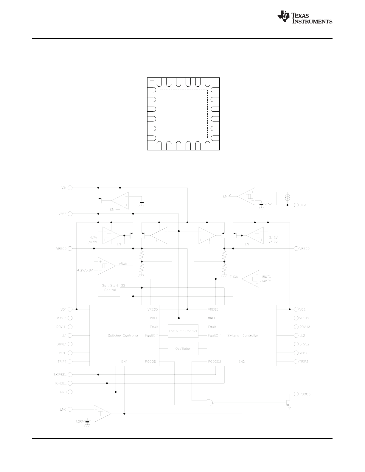
TPS51123RGE
(QFN-24)
VO1
PGOOD
VO2
VREG3
VBST1
DRVL1
LL1
DRVH1
VBST2
DRVH2
LL2
DRVL2
EN0
TRIP2
VFB2
VREF
TONSEL
VFB1
TRIP1
SKIPSEL
GND
VIN
ENC
VREG5
2
3
4
5
6
7 8
9 10
11
1
12
13
14
15
16
17
18
24 23
22 21
20 19
TPS51123
SLUS890E –DECEMBER 2008–REVISED JANUARY 2013
www.ti.com
QFN PACKAGE (TOP VIEW)
Functional Block Diagram
8 Submit Documentation Feedback Copyright © 2008–2013, Texas Instruments Incorporated
Product Folder Links: TPS51123
TPS51123
www.ti.com
SLUS890E –DECEMBER 2008–REVISED JANUARY 2013
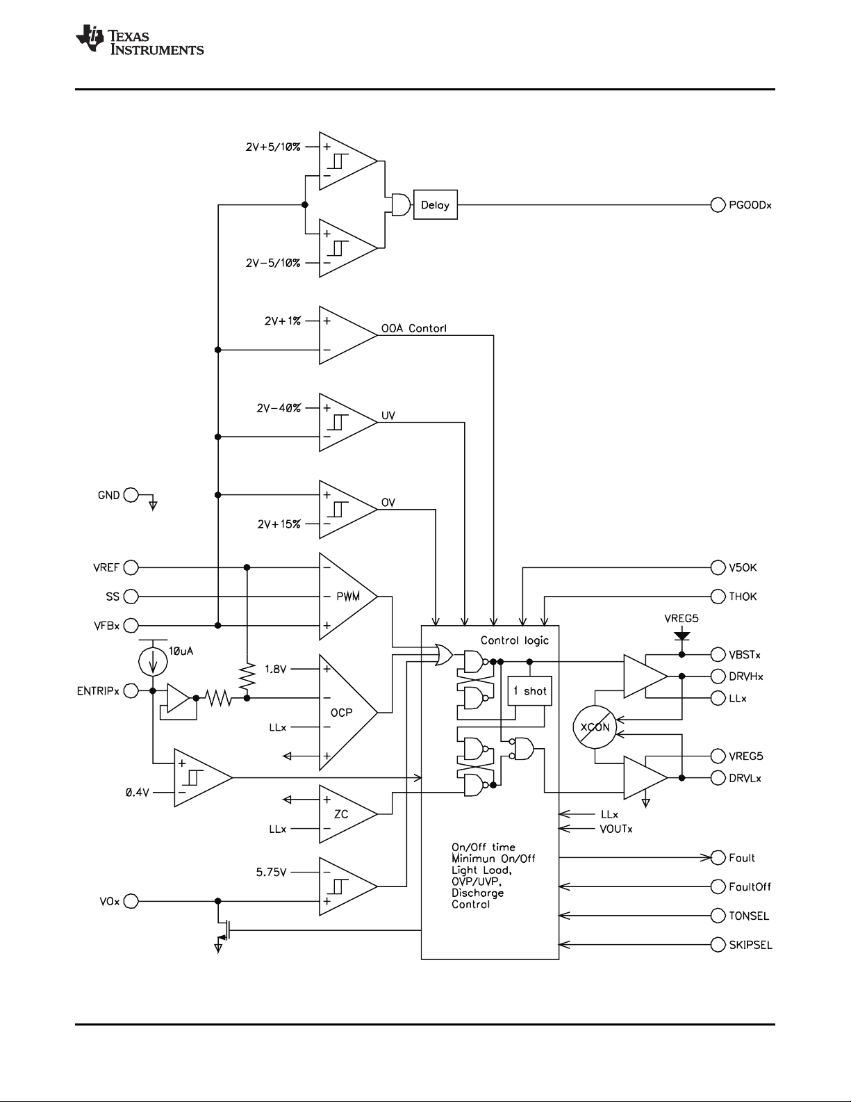
Switcher Controller Block
Copyright © 2008–2013, Texas Instruments Incorporated Submit Documentation Feedback 9
Product Folder Links: TPS51123
VIN SUPPLY CURRENT2
vs
JUNCTION TEMPERATURE
0
1
2
3
4
5
6
7
8
9
-50 0 50 100 150
TJ- Junction Temperature - °C
I
VIN2
- VIN Supply Current2 - mA
VIN SUPPLY CURRENT2
vs
INPUT VOLTAGE
0
1
2
3
4
5
6
7
8
9
5 10 15 20 25
VIN- Input Voltage - V
I
VIN2
- VIN Supply Current2 - mA
VIN SUPPLY CURRENT1
vs
INPUT VOLTAGE
0
100
200
300
400
500
600
700
800
5 10 15 20 25
VIN- Input Voltage - V
I
VIN1
- VIN Supply Current1 - mA
VIN SUPPLY CURRENT1
vs
JUNCTION TEMPERATURE
0
100
200
300
400
500
600
700
800
-50 0 50 100 150
TJ- Junction Temperature - °C
I
VIN1
- VIN Supply Current1 - mA
TPS51123
SLUS890E –DECEMBER 2008–REVISED JANUARY 2013
TYPICAL CHARACTERISTICS
www.ti.com
10 Submit Documentation Feedback Copyright © 2008–2013, Texas Instruments Incorporated
Figure 1. Figure 2.
Figure 3. Figure 4.
Product Folder Links: TPS51123
VIN SHUTDOWN CURRENT
vs
INPUT VOLTAGE
0
5
10
15
20
25
5 10 15 20 25
VIN- Input Voltage - V
I
VINSDN
- VIN Shutdown Current - mA
VIN SHUTDOWN CURRENT
vs
JUNCTION TEMPERATURE
0
5
10
15
20
25
-50 0 50 100 150
TJ- Junction Temperature - °C
I
VINS DN
- VIN Shutdown Current - mA
VIN STANDBY CURRENT
vs
JUNCTION TEMPERATURE
0
50
100
150
200
250
-
50
0 50 100 150
TJ- Junction Temperature - °C
I
VINST BY
- VIN Standby Cu rrent - mA
VINSTANDBY CURRENT
vs
INPUTVOLTAGE
0
50
100
150
200
250
5 10 15 20 25
VIN-InputVoltage-V
I
VINST BY
- VIN Standby Current -
nA
TPS51123
www.ti.com
SLUS890E –DECEMBER 2008–REVISED JANUARY 2013
TYPICAL CHARACTERISTICS (continued)
Figure 5. Figure 6.
Copyright © 2008–2013, Texas Instruments Incorporated Submit Documentation Feedback 11
Figure 7. Figure 8.
Product Folder Links: TPS51123
SWITCHINGFREQUENCY
vs
INPUTVOLTAGE
0
100
200
300
400
500
6 8 10 12 14 16 18 20 22 24 26
VIN-InputVoltage-V
f
SW
- Swithching Frequency - kHz
TONSEL =2V
CH1
CH2
SWITCHINGFREQUENCY
vs
INPUTVOLTAGE
0
100
200
300
400
500
6 8 10 12 14 16 18 20 22 24 26
VIN-InputVoltage-V
f
SW
- Swithching Frequency - kHz
TONSEL =3.3V
CH1
CH2
CURRENT SENSE CURRENT
vs
JUNCTION TEMPERATURE
6
7
8
9
10
11
12
13
14
-
50
0 50 100 150
TJ- Junction Temperature - °C
- Current Sense Current - mA
I
TRIP
SWITCHINGFREQUENCY
vs
INPUTVOLTAGE
0
100
200
300
400
500
6 8 10 12 14 16 18 20 22 24 26
VIN-InputVoltage-V
f
SW
- Swithching Frequency - kHz
TONSEL =GND
CH1
CH2
TPS51123
SLUS890E –DECEMBER 2008–REVISED JANUARY 2013
TYPICAL CHARACTERISTICS (continued)
Figure 9. Figure 10.
www.ti.com
12 Submit Documentation Feedback Copyright © 2008–2013, Texas Instruments Incorporated
Figure 11. Figure 12.
Product Folder Links: TPS51123
SWITCHINGFREQUENCY
vs
OUTPUTCURRENT
0
100
200
300
400
500
0.001 0.01 0.1 1 10
I
OUT
-OutputCurrent- A
f
SW
- Swithching Frequency - kHz
TONSEL =2V
CH2 Auto-skip
CH2OOA
CH2PWMOnly
CH1PWMOnly
CH1 Auto-skip
CH1OOA
SWITCHINGFREQUENCY
vs
OUTPUTCURRENT
0
100
200
300
400
500
0.001 0.01 0.1 1 10
I
OUT
-OutputCurrent- A
f
SW
- Swithching Frequency - kHz
TONSEL =3.3V
CH2 Auto-skip
CH2OOA
CH2PWMOnly
CH1PWMOnly
CH1 Auto-skip
CH1OOA
SWITCHINGFREQUENCY
vs
INPUTVOLTAGE
0
100
200
300
400
500
6 8 10 12 14 16 18 20 22 24 26
VIN-InputVoltage-V
f
SW
- Swithching Frequency - kHz
TONSEL =5V
CH1
CH2
SWITCHINGFREQUENCY
vs
OUTPUTCURRENT
0
100
200
300
400
500
0.001 0.01 0.1 1 10
I
OUT
-OutputCurrent- A
f
SW
- Swithching Frequency - kHz
TONSEL =GND
CH2 Auto-skip
CH2OOA
CH2PWMOnly
CH1PWMOnly
CH1 Auto-skip
CH1OOA
TPS51123
www.ti.com
SLUS890E –DECEMBER 2008–REVISED JANUARY 2013
TYPICAL CHARACTERISTICS (continued)
Figure 13. Figure 14.
Copyright © 2008–2013, Texas Instruments Incorporated Submit Documentation Feedback 13
Figure 15. Figure 16.
Product Folder Links: TPS51123

VREG5 OUTPUT VOLTAGE
vs
OUTPUT CURRENT
4.90
4.95
5.00
5.05
0 20 40 60 80 100
I
VREG5
- VREG5 Output Cur re nt - m A
V
VREG5
- VREG5 Outp ut Voltage - V
VREG3 OUTPUT VOLTAGE
vs
OUTPUT CURRENT
3.2
3.25
3.3
3.35
0 20 40 60 80 100
I
VREG3
- VREG3 Output Cur re nt - m A
VVR EG3 - VREG3 Output Voltage - V
SWITCHINGFREQUENCY
vs
OUTPUTCURRENT
0
100
200
300
400
500
0.001 0.01 0.1 1 10
I
OUT
-OutputCurrent- A
f
SW
- Swithching Frequency - kHz
TONSEL =5V
CH2 Auto-skip
CH2OOA
CH2PWMOnly
CH1PWMOnly
CH1 Auto-skip
CH1OOA
OVP/UVP THRESHOLD VOLTAGE
vs
JUNCTION TEMPERATURE
40
50
60
70
80
90
100
110
120
130
140
150
-50 0 50 100 150
TJ- Junction Temperature - °C
V
OVP/VUV P
- OVP/UVP Threshold - %
TPS51123
SLUS890E –DECEMBER 2008–REVISED JANUARY 2013
TYPICAL CHARACTERISTICS (continued)
Figure 17. Figure 18.
www.ti.com
14 Submit Documentation Feedback Copyright © 2008–2013, Texas Instruments Incorporated
Figure 19. Figure 20.
Product Folder Links: TPS51123

3.3-VOUTPUTVOLTAGE
vs
OUTPUTCURRENT
3.240
3.270
3.300
3.330
3.360
0.001 0.01 0.1 1 10
I
OUT2
-3.3-VOutputCurrent- A
V
OUT2
- 3.3-V Outp ut Voltage - V
PWMOnly
Auto-skip
OOA
5-VOUTPUTVOLTAGE
vs
INPUTVOLTAGE
4.950
4.975
5.000
5.025
5.050
5.075
6 8 10 12 14 16 18 20 22 24 26
VIN-InputVoltage-V
V
OUT1
- 5-V Out put Voltag e - V
IO=0A
IO=6A
VREF OUTPUT VOLTAGE
vs
OUTPUT CURRENT
1.980
1.985
1.990
1.995
2.000
2.005
2.010
2.015
2.020
0 20 40 60 80 100
I
VREF
- VREF Output Current - mA
V
VREF
- VREF Output Voltage - V
5-V OUTPUT VOLTAGE
vs
OUTPUT CURRENT
4.950
4.975
5.000
5.025
5.050
5.075
0.001 0.01 0.1 1 10
I
OUT1
- 5-V Output Current - A
V
OUT1
- 5-V Output Voltage - V
PWM Only
Auto-skip
OOA
TPS51123
www.ti.com
SLUS890E –DECEMBER 2008–REVISED JANUARY 2013
TYPICAL CHARACTERISTICS (continued)
Copyright © 2008–2013, Texas Instruments Incorporated Submit Documentation Feedback 15
Figure 21. Figure 22.
Figure 23. Figure 24.
Product Folder Links: TPS51123

3.3-V EFFICIENCY
vs
OUTPUT CURRENT
0
20
40
60
80
100
0.001 0.01 0.1 1 10
I
OUT2
- 3.3-V Output Current - A
h - Efficiency - %
Auto-skip
PWM Only
OOA
5-V Switcher ON
VIN=8V
VIN=12V
VIN=20V
3.3-VOUTPUTVOLTAGE
vs
INPUTVOLTAGE
3.240
3.270
3.300
3.330
3.360
6 8 10 12 14 16 18 20 22 24 26
VIN-InputVoltage-V
V
OUT2
- 3.3-V Outp ut Voltage - V
IO=0A
IO=6A
0
20
40
60
80
100
0.001 0.01 0.1 1 10
h – Efficiency – %
VIN= 20 V
VIN= 12 V
VIN= 8 V
OOA
Auto-Skip
PWM Only
I
OUT1
– 5-V Output Current – A
5-V EFFICIENCY
vs
OUTPUT CURRENT
TPS51123
SLUS890E –DECEMBER 2008–REVISED JANUARY 2013
TYPICAL CHARACTERISTICS (continued)
Figure 25. Figure 26.
www.ti.com
16 Submit Documentation Feedback Copyright © 2008–2013, Texas Instruments Incorporated
Figure 27.
Product Folder Links: TPS51123

ENC (5 V/div)
V
OUT1
(2 V/div)
PGOOD (5 V/div)
ENC (5 V/div)
V
OUT2
(2 V/div)
PGOOD (5 V/div)
V
OUT1
(100mV/div)
I
IND
(5A/div)
I
OUT1
(5A/div)
V
OUT2
(100mV/div)
I
IND
(5A/div)
I
OUT2
(5A/div)
TPS51123
www.ti.com
SLUS890E –DECEMBER 2008–REVISED JANUARY 2013
TYPICAL CHARACTERISTICS (continued)
5-V Load Transient Response 3.3-V Load Transient Response
Figure 28. Figure 29.
5-V Startup Waveforms 3.3-V Startup Waveforms
Figure 30. Figure 31.
Copyright © 2008–2013, Texas Instruments Incorporated Submit Documentation Feedback 17
Product Folder Links: TPS51123

ENC (10 V/div)
V
OUT1
(2 V/div)
PGOOD (5 V/div)
DRVL1 (5 V/div)
ENC (10 V/div)
V
OUT2
(2 V/div)
PGOOD (5 V/div)
DRVL2 (5 V/div)
V
OUT1
(200mV/div)
VREG5 (200mV/div)
V
OUT2
(200mV/div)
VREG3 (200mV/div)
TPS51123
SLUS890E –DECEMBER 2008–REVISED JANUARY 2013
TYPICAL CHARACTERISTICS (continued)
5-V Switchover Waveforms 3.3-V Switchover Waveforms
Figure 32. Figure 33.
5-V Soft-stop Waveforms 3.3-V Soft-stop Waveforms
www.ti.com
18 Submit Documentation Feedback Copyright © 2008–2013, Texas Instruments Incorporated
Figure 34. Figure 35.
Product Folder Links: TPS51123

TPS51123
www.ti.com
SLUS890E –DECEMBER 2008–REVISED JANUARY 2013
APPLICATION INFORMATION
PWM Operations
The main control loop of the switch mode power supply (SMPS) is designed as an adaptive on-time pulse width
modulation (PWM) controller. It supports a proprietary D-CAP™ mode. D-CAP™ mode does not require external
compensation circuit and is suitable for low external component count configuration when used with appropriate
amount of ESR at the output capacitor(s).
At the beginning of each cycle, the synchronous top MOSFET is turned on, or becomes ‘ON’ state. This
MOSFET is turned off, or becomes ‘OFF’ state, after internal one shot timer expires. This one shot is determined
by VINand V
to keep frequency fairly constant over input voltage range, hence it is called adaptive on-time
OUT
control. The MOSFET is turned on again when the feedback point voltage, VFB, decreased to match with internal
2-V reference. The inductor current information is also monitored and should be below the over current threshold
to initiate this new cycle. Repeating operation in this manner, the controller regulates the output voltage. The
synchronous bottom or the “rectifying” MOSFET is turned on at the beginning of each ‘OFF’ state to keep the
conduction loss minimum.The rectifying MOSFET is turned off before the top MOSFET turns on at next switching
cycle or when inductor current information detects zero level. In the auto-skip mode or the OOA skip mode, this
enables seamless transition to the reduced frequency operation at light load condition so that high efficiency is
kept over broad range of load current.
Adaptive On-Time Control and PWM Frequency
TPS51123 does not have a dedicated oscillator on board. However, the part runs with pseudo-constant
frequency by feed-forwarding the input and output voltage into the on-time, one-shot timer. The on-time is
controlled inverse proportional to the input voltage and proportional to the output voltage so that the duty ratio will
be kept as VOUT/VIN technically with the same cycle time. The frequencies are set by TONSEL terminal
connection as Table 2.
Table 2. TONSEL Connection and Switching Frequency
TONSEL CONNECTION
GND 200 250
VREF 245 305
VREG3 300 375
VREG5 365 460
SWITCHING FREQUENCY (kHz)
CH1 CH2
Copyright © 2008–2013, Texas Instruments Incorporated Submit Documentation Feedback 19
Product Folder Links: TPS51123

f
SW
0
O
1
f
2 ESR C 4
= £
p ´ ´
ESR
R1
Co
+
2V
+
Lx
R2
Control
logic
&
Driver
RL
VIN
VFB
DRVH
DRVL
PWM
Switching ModulatorVoltage Divider
IoIc
I
L
Vc
Output Capacitor
TPS51123
SLUS890E –DECEMBER 2008–REVISED JANUARY 2013
Loop Compensation
From small-signal loop analysis, a buck converter using D-CAPTMmode can be simplified as below.
Figure 36. Simplifying the Modulator
www.ti.com
The output voltage is compared with internal reference voltage after divider resistors, R1 and R2. The PWM
comparator determines the timing to turn on high-side MOSFET. The gain and speed of the comparator is high
enough to keep the voltage at the beginning of each on cycle substantially constant. For the loop stability, the
0dB frequency, f0, defined below need to be lower than 1/4 of the switching frequency.
As f0is determined solely by the output capacitor's characteristics, loop stability of D-CAPTMmode is determined
by the capacitor's chemistry. For example, specialty polymer capacitors (SP-CAP) have Co in the order of
several 100 μF and ESR in range of 10 mΩ. These make f0on the order of 100 kHz or less and the loop will be
stable. However, ceramic capacitors have f0at more than 700 kHz, which is not suitable for this operational
mode.
Ramp Signal
The TPS51123 adds a ramp signal to the 2-V reference in order to improve its jitter performance. As described in
the previous section, the feedback voltage is compared with the reference information to keep the output voltage
in regulation. By adding a small ramp signal to the reference, the S/N ratio at the onset of a new switching cycle
is improved. Therefore the operation becomes less jitter and stable. The ramp signal is controlled to start with 20mV at the beginning of ON-cycle and to become 0 mV at the end of OFF-cycle in steady state. By using this
scheme, the TPS51123 improve jitter performance without sacrificing the reference accuracy.
(1)
20 Submit Documentation Feedback Copyright © 2008–2013, Texas Instruments Incorporated
Product Folder Links: TPS51123

( )
f
IN OUT OUT
OUT(LL)
IN
1
I
2 L
V V V
V
´
´ ´
- ´
=
TPS51123
www.ti.com
SLUS890E –DECEMBER 2008–REVISED JANUARY 2013
Light Load Condition in Auto-Skip Operation
The TPS51123 automatically reduces switching frequency at light load conditions to maintain high efficiency.
This reduction of frequency is achieved smoothly and without increase of V
ripple. Detail operation is
OUT
described as follows. As the output current decreases from heavy load condition, the inductor current is also
reduced and eventually comes to the point that its ‘valley’ touches zero current, which is the boundary between
continuous conduction and discontinuous conduction modes. The rectifying MOSFET is turned off when this zero
inductor current is detected. As the load current further decreased, the converter runs in discontinuous
conduction mode and it takes longer and longer to discharge the output capacitor to the level that requires next
‘ON’ cycle. The ON time is kept the same as that in the heavy load condition. In reverse, when the output current
increase from light load to heavy load, switching frequency increases to the preset value as the inductor current
reaches to the continuous conduction. The transition load point to the light load operation I
OUT(LL)
(i.e. the
threshold between continuous and discontinuous conduction mode) can be calculated as follows;
(2)
where f is the PWM switching frequency.
Switching frequency versus output current in the light load condition is a function of L, VINand V
decreases almost proportional to the output current from the I
kHz at I
/5 if the frequency setting is 300 kHz.
OUT(LL)
shown in Equation 2. For example, it ise 60
OUT(LL)
OUT
, but it
Out-of-Audio™ Light-Load Operation
Out-of-Audio™ (OOA) light-load mode is a unique control feature that keeps the switching frequency above
acoustic audible frequencies toward virtually no load condition while maintaining best of the art high conversion
efficiency. When the Out-of-Audio™ operation is selected, OOA control circuit monitors the states of both
MOSFET and force to change into the ‘ON’ state if both of MOSFETs are off for more than 32 μs. This means
that the top MOSFET is turned on even if the output voltage is higher than the target value so that the output
capacitor is tends to be overcharged.
The OOA control circuit detects the over-voltage condition and begins to modulate the on time to keep the output
voltage regulated. As a result, the output voltage becomes 0.5% higher than normal light-load operation.
Enable and Soft Start
EN0 is the control pin of VREG5, VREG3 and VREF regulators. Bring this node down to GND disables those
three regulators and minimize the shutdown supply current to 10 μA. Pulling this node up to 3.3 V or 5 V will turn
the three regulators on to standby mode. The two switch mode power supplies (channel-1, channel-2) become
ready to enable at this standby mode. The TPS51123 has an internal, 1.6 ms, voltage servo softstart for each
channel. When the ENC pin becomes higher than the enable threshold voltage, which is typically 1.26 V, an
internal DAC begins ramping up the reference voltage to both of the PWM comparators at the same time.
Smooth control of the output voltage is maintained during start up.
Table 3. Enabling State
EN0 ENC VREF VREG5 VREG3 CH1 CH2
GND Don’t Care Off Off Off Off Off
Open Off On On On Off Off
Open On On On On On On
VREG5/VREG3 Linear Regulators
There are two sets of 100-mA standby linear regulators which outputs 5 V and 3.3 V, respectively. The VREG5
serves as the main power supply for the analog circuitry of the device and provides the current for gate drivers.
The VREG3 is intended mainly for auxiliary 3.3-V supply for the notebook system during standby mode.
Add a ceramic capacitor with a value of at least 33 μF and place it close to the VREG5 pin, and add at most
10 μF to the VREG3 pin. Total capacitance connected to the VREG3 pin should not exceed 10 μF .
Copyright © 2008–2013, Texas Instruments Incorporated Submit Documentation Feedback 21
Product Folder Links: TPS51123

TPS51123
SLUS890E –DECEMBER 2008–REVISED JANUARY 2013
www.ti.com
VREG5 Switch Over
When the VO1 voltage becomes higher than 4.7 V AND channel-1 internal powergood flag is generated, internal
5-V LDO regulator is shut off and the VREG5 output is connected to VO1 by internal switch over MOSFET. The
510-μs powergood delay helps a switch over without glitch.
VREG3 Switch Over
When the VO2 voltage becomes higher than 3.15 V AND channel-2 internal powergood flag is generated,
internal 3.3-V LDO regulator is shut off and the VREG3 output is connected to VO2 by internal switch over
MOSFET. The 510-μs powergood delay helps a switch over without glitch.
Powergood
The TPS51123 has one powergood output that indicates 'high' when both switcher outputs are within the targets
(AND gated). The powergood function is activated with 2-ms internal delay after ENC goes high. If the output
voltage becomes within ±5% of the target value, internal comparators detect power good state and the
powergood signal becomes high after 510-μs internal delay. Therefore PGOOD goes high around 2.5 ms after
ENC goes high. If the output voltage goes outside of ±10% of the target value, the powergood signal becomes
low after 2-μs internal delay. The powergood output is an open drain output and is needed to be pulled up
outside.
Also note that, in the case of Auto-skip or Out-of-Audio™ mode, if the output voltage goes +10% above the
target value and the power-good signal flags low, then the loop attempts to correct the output by turning on the
low-side driver (forced PWM mode). After the feedback voltage returns to be within +5% of the target value and
the power-good signal goes high, the controller returns back to auto-skip mode or Out-of-Audio™ mode.
Output Discharge Control
When ENC is low, the TPS51123 discharges outputs using internal MOSFET which is connected to VOx and
GND. The current capability of these MOSFETs is limited to discharge slowly.
Low-Side Driver
The low-side driver is designed to drive high current low R
represented by its internal resistance, which are 4 Ω for VREG5 to DRVLx and 1.5 Ω for DRVLx to GND. A dead
time to prevent shoot through is internally generated between top MOSFET off to bottom MOSFET on, and
bottom MOSFET off to top MOSFET on. 5-V bias voltage is delivered from VREG5 supply. The instantaneous
drive current is supplied by an input capacitor connected between VREG5 and GND. The average drive current
is equal to the gate charge at Vgs = 5 V times switching frequency. This gate drive current as well as the highside gate drive current times 5 V makes the driving power which need to be dissipated from TPS51123 package.
N-channel MOSFET(s). The drive capability is
DS(on)
High-Side Driver
The high-side driver is designed to drive high current, low R
floating driver, 5-V bias voltage is delivered from VREG5 supply. The average drive current is also calculated by
the gate charge at Vgs = 5 V times switching frequency. The instantaneous drive current is supplied by the flying
capacitor between VBSTx and LLx pins. The drive capability is represented by its internal resistance, which are 4
Ω for VBSTx to DRVHx and 1.5Ω for DRVHx to LLx.
N-channel MOSFET(s). When configured as a
DS(on)
22 Submit Documentation Feedback Copyright © 2008–2013, Texas Instruments Incorporated
Product Folder Links: TPS51123

( ) ( )
( )
f
IN OUT OUT
TRIP RIPPLE TRIP
OCP
IN
DS on DS on
V V V
V I V
1
I
R 2 R 2 L V
- ´
= + = + ´
´ ´
( )
( ) ( )
( )
TRIP TRIP
TRIP
R k I A
V mV 24 mV
9
W ´ m
= -
TPS51123
www.ti.com
SLUS890E –DECEMBER 2008–REVISED JANUARY 2013
Current Protection
TPS51123 has cycle-by-cycle over current limiting control. The inductor current is monitored during the ‘OFF’
state and the controller keeps the ‘OFF’ state during the inductor current is larger than the over current trip level.
In order to provide both good accuracy and cost effective solution, TPS51123 supports temperature
compensated MOSFET R
setting resistor, R
. TRIPx terminal sources I
TRIP
trip level is set to the OCL trip voltage V
internally.
Note that when TRIPx voltage is under a certain thershould (typically 0.4V), the switcher channel concerned is
shut down. The inductor current is monitored by the voltage between GND pin and LLx pin so that LLx pin should
be connected to the drain terminal of the bottom MOSFET properly. Itrip has 4500 ppm/°C temperature slope to
compensate the temperature dependency of the R
that GND should be connected to the proper current sensing device, i.e. the source terminal of the bottom
MOSFET.
As the comparison is done during the ‘OFF’ state, V
current at over current threshold, I
In an over current condition, the current to the load exceeds the current to the output capacitor thus the output
voltage tends to fall down. Eventually, it ends up with crossing the under voltage protection threshold and
shutdown both channels.
sensing. The TRIPx pin should be connected to GND through the trip voltage
DS(on)
TRIP
, can be calculated as follows;
OCP
current, which is 10 μA typically at room temperature, and the
TRIP
as below. Note that the V
. GND is used as the positive current sensing node so
DS(on)
sets valley level of the inductor current. Thus, the load
TRIP
is limited up to about 205 mV
TRIP
(3)
(4)
Overvoltage and Undervoltage Protection
TPS51123 monitors a resistor divided feedback voltage to detect over and under voltage. When the feedback
voltage becomes higher than 115% of the target voltage, the OVP comparator output goes high and the circuit
latches as the top MOSFET driver OFF and the bottom MOSFET driver ON.
Also, TPS51123 monitors VOx voltage directly and if it becomes greater than 5.75 V the TPS51123 turns off the
top MOSFET driver.
When the feedback voltage becomes lower than 60% of the target voltage, the UVP comparator output goes
high and an internal UVP delay counter begins counting. After 32 μs, TPS51123 latches OFF both top and
bottom MOSFETs drivers, and shut off both drivers of another channel. This function is enabled after 2 ms
following ENC has become high.
Copyright © 2008–2013, Texas Instruments Incorporated Submit Documentation Feedback 23
Product Folder Links: TPS51123

( ) ( )
( )
( )
( )
f
OUT
RIPPLE
V 20 mV 1 D 20 mV L
ESR
2 V I 2 V
´ ´ - ´ ´
= -
´
( )
( )
( )
(
)
( )
f
OUT OUT
IN m ax
TRIP
IND peak
DS on IN m ax
V
1
R L
V V V
I
V´
- ´
= + ´
( )
( )
(
)
( )
( )
( )
(
)
( )
f f
OUT OUT OUT OUT
IN max IN max
IND ripple IN max OUT max IN max
1 3
I I
V V V V V V
L
V V
´
´ ´
- ´ - ´
= = ´
( )
OUT
V 2.0
R1 R2
2.0
-
= ´
TPS51123
SLUS890E –DECEMBER 2008–REVISED JANUARY 2013
www.ti.com
UVLO Protection
TPS51123 has VREG5 under voltage lock out protection (UVLO). When the VREG5 voltage is lower than UVLO
threshold voltage both switch mode power supplies are shut off. This is non-latch protection. When the VREG3
voltage is lower than (VO2 - 1 V), both switch mode power supplies are also shut off
Thermal Shutdown
TPS51123 monitors the temperature of itself. If the temperature exceeds the threshold value (typically 150°C),
TPS51123 is shut off including LDOs. This is non-latch protection.
External Parts Selection
The external components selection is much simple in D-CAP™ Mode.
1. Determine output voltage
The output voltage is programmed by the voltage-divider resistor, R1 and R2, as shown in Figure 36. R1 is
connected between VFBx pin and the output, and R2 is connected betwen the VFBx pin and GND.
Recommended R2 value is from 10 kΩ to 20 kΩ. Determine R1 using equation as below.
(5)
2. Choose the Inductor
The inductance value should be determined to give the ripple current of approximately 1/4 to 1/2 of maximum
output current. Larger ripple current increases output ripple voltage and improves S/N ratio and helps stable
operation.
(6)
The inductor also needs to have low DCR to achieve good efficiency, as well as enough room above peak
inductor current before saturation. The peak inductor current can be estimated as follows.
(7)
3. Choose the Output Capacitor(s)
Organic semiconductor capacitor(s) or specialty polymer capacitor(s) are recommended. Determine ESR to meet
required ripple voltage. A quick approximation is as shown in Equation 8. This equation is based on that required
output ripple slope is approximately 20 mV per TSW(switching period) in terms of VFB terminal voltage.
where
• D is the duty cycle
• the required output ripple slope is approximately 20 mV per tSW(switching period) in terms of VFB terminal
voltage (8)
4. Choose the Low-Side MOSFET
It is highly recommended that the low-side MOSFET should have an integrated Schottky barrier diode, or an
external Schottky barrier diode in parallel to achieve stable operation.
24 Submit Documentation Feedback Copyright © 2008–2013, Texas Instruments Incorporated
Product Folder Links: TPS51123

TPS51123
www.ti.com
SLUS890E –DECEMBER 2008–REVISED JANUARY 2013
Layout Considerations
Certain points must be considered before starting a layout work using the TPS51123.
• TPS51123 has only one GND pin and special care of GND trace design makes operation stable, especially
when both channels operate. Group GND terminals of output voltage divider of both channels and the VREF
capacitor as close as possible, and connect them to an inner GND plane with PowerPad and the overcurrent
setting resistor, as shown in the thin GND line of Figure 37. This trace is named Signal Ground (SGND).
Group ground terminals of VIN capacitor(s), VOUT capacitor(s) and source of low-side MOSFETs as close as
possible, and connect them to another inner GND plane with GND pin of the device and the GND terminal of
VREG3 and VREG5 capacitors, as shown in the bold GND line of Figure 37. This trace is named Power
Ground (PGND). SGND should be connected to PGND at the middle point between ground terminal of VOUT
capacitors.
• Inductor, VOUT capacitor(s), VIN capacitor(s) and MOSFETs are the power components and should be
placed on one side of the PCB (solder side). Power components of each channel should be at the same
distance from the TPS51123. Other small signal parts should be placed on another side (component side).
Inner GND planes should shield and isolate the small signal traces from noisy power lines.
• PCB trace defined as LLx node, which connects to source of high-side MOSFET, drain of low-side MOSFET
and high-voltage side of the inductor, should be as short and wide as possible.
• VREG5 requires capacitance of at least 33-μF and VREG3 requires capacitance of at most 10-μF. VREF
requires a 220-nF ceramic bypass capacitor which should be placed close to the device and traces should be
no longer than 10 mm.
• Connect the overcurrent setting resistors from TRIPx to SGND and close to the device, right next to the
device if possible.
• The discharge path (VOx) should have a dedicated trace to the output capacitor; separate from the output
voltage sensing trace. When LDO5 is switched over Vo1 trace should be 1.5 mm with no loops. When LDO3
is switched over and loaded Vo2 trace should also be 1.5 mm with no loops. There is no restriction for just
monitoring Vox. Make the feedback current setting resistor (the resistor between VFBx to SGND) close to the
device. Place on the component side and avoid vias between this resistor and the device.
• Connections from the drivers to the respective gate of the high-side or the low-side MOSFET should be as
short as possible to reduce stray inductance. Use 0.65-mm (25 mils) or wider trace and via(s) of at least 0.5
mm (20 mils) diameter along this trace.
• All sensitive analog traces and components such as VOx, VFBx, VREF, GND, EN0, TRIPx, PGOOD,
TONSEL and SKIPSEL should be placed away from high-voltage switching nodes such as LLx, DRVLx, and
DRVHx nodes to avoid coupling.
• Traces for VFB1 and VFB2 should be short and laid apart each other to avoid channel to channel
interference.
• In order to effectively remove heat from the package, prepare thermal land and solder to the package’s
thermal pad. Three by three or more vias with a 0.33-mm (13 mils) diameter connected from the thermal land
to the internal ground plane should be used to help dissipation. This thermal land underneath the package
should be connected to SGND, and should NOT be connected to PGND.
Copyright © 2008–2013, Texas Instruments Incorporated Submit Documentation Feedback 25
Product Folder Links: TPS51123

TPS51123
DRVL1DRVL2
PowerPAD
VFB1VFB2 VREF
GND
VREG5
VREG3
220 nF
SGND
SGND
UDG-08166
5 3 2
5 19
15
33 mF
817
10 mF
V
IN
V
IN
V
OUT1
V
OUT2
PGND PGND
TPS51123
SLUS890E –DECEMBER 2008–REVISED JANUARY 2013
www.ti.com
Figure 37. Ground System
26 Submit Documentation Feedback Copyright © 2008–2013, Texas Instruments Incorporated
Product Folder Links: TPS51123

Driver and switch node traces are shown for CH1 only.
*
Cin
Cin
L
L
Vout1
HS-MOSFET
LS-MOSFET
HS-MOSFET
Vout2
Cout
To CH1 Vout divider
To CH2 Vout divider
To VO2
To VO1
LS-MOSFET
Bottom Layer
VIN
GND
Connection to GND island
Connection to GND
Connection of Vout
Top Layer
TPS51123
C
VREF
CH1 Vout divider
C
VREG5
DRVH1*
LL1*
DRVL1*
Through hole
CH2 Vout divider
Connection to
GND island
GND
Inner Layer
C
VREG3
Cout
GND island
TPS51123
www.ti.com
SLUS890E –DECEMBER 2008–REVISED JANUARY 2013
Figure 38. PCB Layout
Copyright © 2008–2013, Texas Instruments Incorporated Submit Documentation Feedback 27
Product Folder Links: TPS51123

9
10
11
12
VO1
PGOOD
VO2
VREG3
TPS51123RGE
(QFN24)
13 14 15 16
VBST1
DRVL1
LL1
DRVH1
VBST2
DRVH2
LL2
DRVL2
17
E
N
0
8
T
R
I
P
2
7
6
V
F
B
2
5
V
R
E
F
4
T
O
N
S
E
L
3
V
F
B
1
2 1
T
R
I
P
1
18
S
K
I
P
S
E
L
19
20
G
N
D
21
V
I
N
22
23
24
E
N
C
VO1
5V/8A
L2
3.3mH
Q3
IRF7821
VO1_GND
PGND
C9
10mF
C7
0.1mF
VIN
VO2
3.3V/8A
L1
3.3mH
Q1
IRF7821
VO2_GND
C4
0.1mF
VIN
PowerPAD
C11
33mF
V
R
E
G
5
C10
POSCAP
330mF
PGND
R9
5.1W
VIN
5.5 ~ 28V
R7
5.1W
C2
10mF
C1
10mF
PGND
C5
POSCAP
330mF
5V/100mA
PGND
R4
30kW
R2
20kW
R1
13kW
SGND
VREG5
VREG5
R8
100kW
PGND
R3
20kW
C6
0.22mF
PGND
SGND
R6
130kW
SGND
R5
130kW
ENC
C3
10mF
PGND
3.3V/100mA
C8
10mF
EN0
PGND
PGND
SGND
Q2
FDS6690AS
Q4
FDS6690AS
UDG-08165
SGND
TPS51123
SLUS890E –DECEMBER 2008–REVISED JANUARY 2013
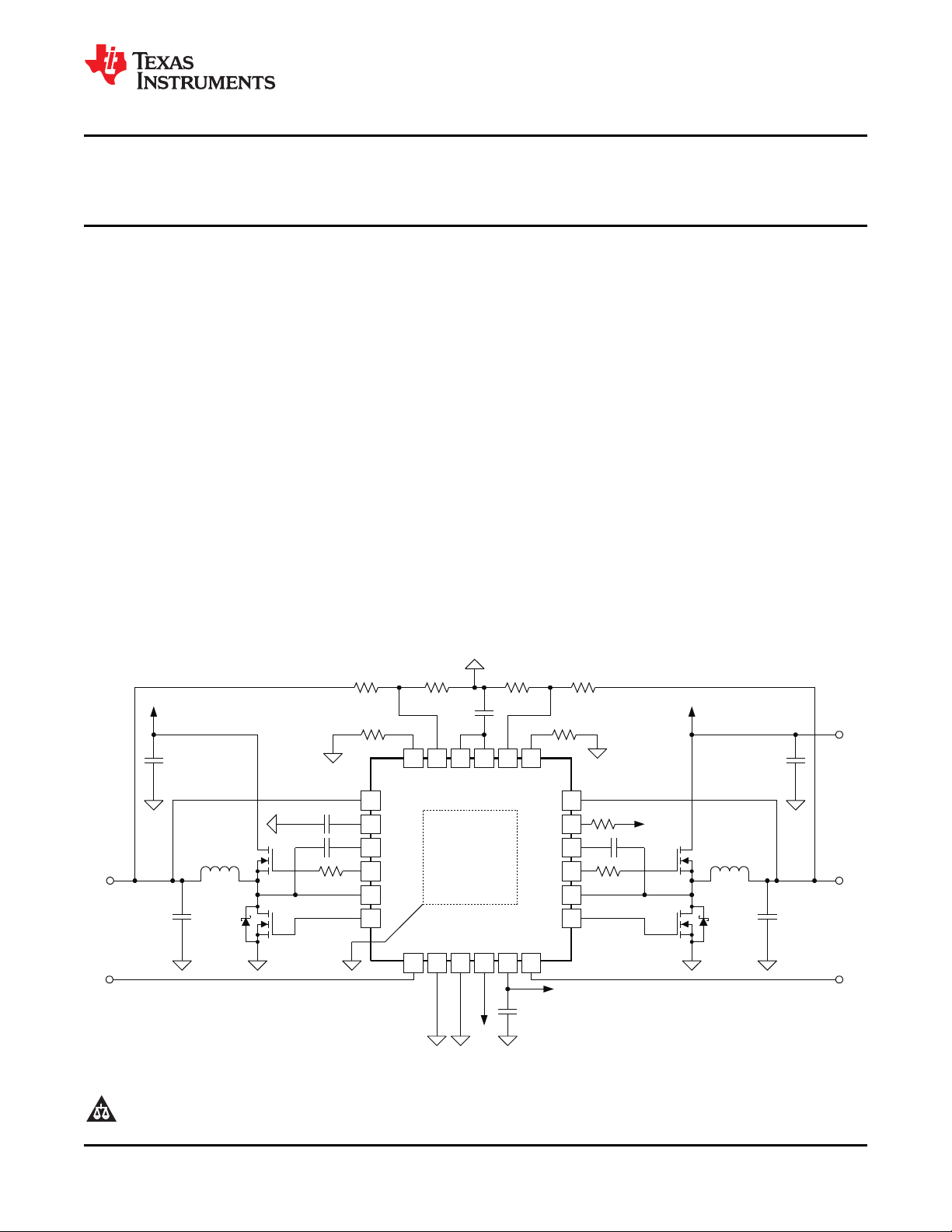
Application Circuit
www.ti.com
Figure 39. 5-V/8-A, 3.3-V/8-A Application Circuit (245-kHz/305-kHz Setting)
Table 4. List of Materials for 5-V/8-A, 3.3-V/8-A Application Circuit
REFERENCE SPECIFICATION MANUFACTURER PART NUMBER
DESIGNATOR
C1, C2, C8, C9 10 μF/25 V Taiyo Yuden TMK325BJ106MM
C3 10 μF/6.3 V TDK C2012X5R0J106K
C11 33 μF/6.3V TDK C3216X5RBJ336M
C5, C10 330 μF/6.3 V/25 mΩ Sanyo 6TPE330ML
L1, L2 3.3 μH, 15.6 A, 5.92 mΩ TOKO FDA1055-3R3M
Q1, Q3 30 V, 9.5 mΩ IR IRF7821
(1)
Q2, Q4
(1) Use a MOSFET with an integrated Schottky barrier diode (SBD) for the low-side, or add an SBD in parallel with a normal MOSFET.
28 Submit Documentation Feedback Copyright © 2008–2013, Texas Instruments Incorporated
30 V, 12 mΩ Fairchild FDS6690AS
Product Folder Links: TPS51123

TPS51123
www.ti.com
SLUS890E –DECEMBER 2008–REVISED JANUARY 2013
REVISION HISTORY
Changes from Revision B (March 2010) to Revision C Page
• Added LL1, LL2, pulse width < 20 ns parameter with a value of -5.0 V to 30 V. ................................................................. 2
Changes from Revision C (March 2012) to Revision D Page
• Added ESD ratings to the ABSOLUTE MAXIMUM RATINGS table .................................................................................... 2
• Added clarity to Switcher Controller Block diagram .............................................................................................................. 9
Changes from Revision D (SEPTEMBER 2012) to Revision E Page
• Added specification for VFB regulation voltage in ELECTRICAL CHARACTERISTICS table ............................................. 4
Copyright © 2008–2013, Texas Instruments Incorporated Submit Documentation Feedback 29
Product Folder Links: TPS51123

PACKAGE OPTION ADDENDUM
www.ti.com
21-Mar-2014
PACKAGING INFORMATION
Orderable Device Status
TPS51123RGER ACTIVE VQFN RGE 24 3000 Green (RoHS
TPS51123RGET ACTIVE VQFN RGE 24 250 Green (RoHS
(1)
The marketing status values are defined as follows:
ACTIVE: Product device recommended for new designs.
LIFEBUY: TI has announced that the device will be discontinued, and a lifetime-buy period is in effect.
NRND: Not recommended for new designs. Device is in production to support existing customers, but TI does not recommend using this part in a new design.
PREVIEW: Device has been announced but is not in production. Samples may or may not be available.
OBSOLETE: TI has discontinued the production of the device.
Package Type Package
(1)
Drawing
Pins Package
Qty
Eco Plan
(2)
& no Sb/Br)
& no Sb/Br)
Lead/Ball Finish
(6)
CU NIPDAU Level-2-260C-1 YEAR -40 to 85 (51123 ~ 51123A)
CU NIPDAU Level-2-260C-1 YEAR -40 to 85 51123
MSL Peak Temp
(3)
Op Temp (°C) Device Marking
(4/5)
(2)
Eco Plan - The planned eco-friendly classification: Pb-Free (RoHS), Pb-Free (RoHS Exempt), or Green (RoHS & no Sb/Br) - please check http://www.ti.com/productcontent for the latest availability
information and additional product content details.
TBD: The Pb-Free/Green conversion plan has not been defined.
Pb-Free (RoHS): TI's terms "Lead-Free" or "Pb-Free" mean semiconductor products that are compatible with the current RoHS requirements for all 6 substances, including the requirement that
lead not exceed 0.1% by weight in homogeneous materials. Where designed to be soldered at high temperatures, TI Pb-Free products are suitable for use in specified lead-free processes.
Pb-Free (RoHS Exempt): This component has a RoHS exemption for either 1) lead-based flip-chip solder bumps used between the die and package, or 2) lead-based die adhesive used between
the die and leadframe. The component is otherwise considered Pb-Free (RoHS compatible) as defined above.
Green (RoHS & no Sb/Br): TI defines "Green" to mean Pb-Free (RoHS compatible), and free of Bromine (Br) and Antimony (Sb) based flame retardants (Br or Sb do not exceed 0.1% by weight
in homogeneous material)
(3)
MSL, Peak Temp. - The Moisture Sensitivity Level rating according to the JEDEC industry standard classifications, and peak solder temperature.
(4)
There may be additional marking, which relates to the logo, the lot trace code information, or the environmental category on the device.
(5)
Multiple Device Markings will be inside parentheses. Only one Device Marking contained in parentheses and separated by a "~" will appear on a device. If a line is indented then it is a continuation
of the previous line and the two combined represent the entire Device Marking for that device.
(6)
Lead/Ball Finish - Orderable Devices may have multiple material finish options. Finish options are separated by a vertical ruled line. Lead/Ball Finish values may wrap to two lines if the finish
value exceeds the maximum column width.
Important Information and Disclaimer:The information provided on this page represents TI's knowledge and belief as of the date that it is provided. TI bases its knowledge and belief on information
provided by third parties, and makes no representation or warranty as to the accuracy of such information. Efforts are underway to better integrate information from third parties. TI has taken and
continues to take reasonable steps to provide representative and accurate information but may not have conducted destructive testing or chemical analysis on incoming materials and chemicals.
TI and TI suppliers consider certain information to be proprietary, and thus CAS numbers and other limited information may not be available for release.
Samples
Addendum-Page 1

PACKAGE OPTION ADDENDUM
www.ti.com
In no event shall TI's liability arising out of such information exceed the total purchase price of the TI part(s) at issue in this document sold by TI to Customer on an annual basis.
21-Mar-2014
Addendum-Page 2
PACKAGE MATERIALS INFORMATION
www.ti.com 12-Aug-2015
TAPE AND REEL INFORMATION
*All dimensions are nominal
Device Package
TPS51123RGER VQFN RGE 24 3000 330.0 12.4 4.25 4.25 1.15 8.0 12.0 Q2
TPS51123RGET VQFN RGE 24 250 180.0 12.4 4.25 4.25 1.15 8.0 12.0 Q2
Type
Package
Drawing
Pins SPQ Reel
Diameter
(mm)
Reel
Width
W1 (mm)
A0
(mm)B0(mm)K0(mm)P1(mm)W(mm)
Pin1
Quadrant
Pack Materials-Page 1
PACKAGE MATERIALS INFORMATION
www.ti.com 12-Aug-2015
*All dimensions are nominal
Device Package Type Package Drawing Pins SPQ Length (mm) Width (mm) Height (mm)
TPS51123RGER VQFN RGE 24 3000 367.0 367.0 35.0
TPS51123RGET VQFN RGE 24 250 210.0 185.0 35.0
Pack Materials-Page 2


IMPORTANT NOTICE
Texas Instruments Incorporated and its subsidiaries (TI) reserve the right to make corrections, enhancements, improvements and other
changes to its semiconductor products and services per JESD46, latest issue, and to discontinue any product or service per JESD48, latest
issue. Buyers should obtain the latest relevant information before placing orders and should verify that such information is current and
complete. All semiconductor products (also referred to herein as “components”) are sold subject to TI’s terms and conditions of sale
supplied at the time of order acknowledgment.
TI warrants performance of its components to the specifications applicable at the time of sale, in accordance with the warranty in TI’s terms
and conditions of sale of semiconductor products. Testing and other quality control techniques are used to the extent TI deems necessary
to support this warranty. Except where mandated by applicable law, testing of all parameters of each component is not necessarily
performed.
TI assumes no liability for applications assistance or the design of Buyers’ products. Buyers are responsible for their products and
applications using TI components. To minimize the risks associated with Buyers’ products and applications, Buyers should provide
adequate design and operating safeguards.
TI does not warrant or represent that any license, either express or implied, is granted under any patent right, copyright, mask work right, or
other intellectual property right relating to any combination, machine, or process in which TI components or services are used. Information
published by TI regarding third-party products or services does not constitute a license to use such products or services or a warranty or
endorsement thereof. Use of such information may require a license from a third party under the patents or other intellectual property of the
third party, or a license from TI under the patents or other intellectual property of TI.
Reproduction of significant portions of TI information in TI data books or data sheets is permissible only if reproduction is without alteration
and is accompanied by all associated warranties, conditions, limitations, and notices. TI is not responsible or liable for such altered
documentation. Information of third parties may be subject to additional restrictions.
Resale of TI components or services with statements different from or beyond the parameters stated by TI for that component or service
voids all express and any implied warranties for the associated TI component or service and is an unfair and deceptive business practice.
TI is not responsible or liable for any such statements.
Buyer acknowledges and agrees that it is solely responsible for compliance with all legal, regulatory and safety-related requirements
concerning its products, and any use of TI components in its applications, notwithstanding any applications-related information or support
that may be provided by TI. Buyer represents and agrees that it has all the necessary expertise to create and implement safeguards which
anticipate dangerous consequences of failures, monitor failures and their consequences, lessen the likelihood of failures that might cause
harm and take appropriate remedial actions. Buyer will fully indemnify TI and its representatives against any damages arising out of the use
of any TI components in safety-critical applications.
In some cases, TI components may be promoted specifically to facilitate safety-related applications. With such components, TI’s goal is to
help enable customers to design and create their own end-product solutions that meet applicable functional safety standards and
requirements. Nonetheless, such components are subject to these terms.
No TI components are authorized for use in FDA Class III (or similar life-critical medical equipment) unless authorized officers of the parties
have executed a special agreement specifically governing such use.
Only those TI components which TI has specifically designated as military grade or “enhanced plastic” are designed and intended for use in
military/aerospace applications or environments. Buyer acknowledges and agrees that any military or aerospace use of TI components
which have not been so designated is solely at the Buyer's risk, and that Buyer is solely responsible for compliance with all legal and
regulatory requirements in connection with such use.
TI has specifically designated certain components as meeting ISO/TS16949 requirements, mainly for automotive use. In any case of use of
non-designated products, TI will not be responsible for any failure to meet ISO/TS16949.
Products Applications
Audio www.ti.com/audio Automotive and Transportation www.ti.com/automotive
Amplifiers amplifier.ti.com Communications and Telecom www.ti.com/communications
Data Converters dataconverter.ti.com Computers and Peripherals www.ti.com/computers
DLP® Products www.dlp.com Consumer Electronics www.ti.com/consumer-apps
DSP dsp.ti.com Energy and Lighting www.ti.com/energy
Clocks and Timers www.ti.com/clocks Industrial www.ti.com/industrial
Interface interface.ti.com Medical www.ti.com/medical
Logic logic.ti.com Security www.ti.com/security
Power Mgmt power.ti.com Space, Avionics and Defense www.ti.com/space-avionics-defense
Microcontrollers microcontroller.ti.com Video and Imaging www.ti.com/video
RFID www.ti-rfid.com
OMAP Applications Processors www.ti.com/omap TI E2E Community e2e.ti.com
Wireless Connectivity www.ti.com/wirelessconnectivity
Mailing Address: Texas Instruments, Post Office Box 655303, Dallas, Texas 75265
Copyright © 2015, Texas Instruments Incorporated

 Loading...