

1
2
3
14
13
12
VBST
DRVH
LL
EN_PSV
TON
VOUT
TPS51117RGY
4
5
6
7
11
10
9
8
TRIP
V5DRV
DRVL
PGND
V5FILT
VFB
PGOOD
GND
+
VOUT
0.75V~5.5V
Q2
L1
Q1
-
PGND
C2
C4
C1
R6
PGOOD
+5V
EN_PSV
R4
R1
R2
R3
R5
VIN
1.8V~28V
C3
GND
+
+
GND
GND
www.ti.com
...................................................................................................................................... SLVS631B –DECEMBER 2005–REVISED SEPTEMBER 2009
SINGLE SYNCHRONOUS STEP-DOWN CONTROLLER
Check for Samples :TPS51117
1
FEATURES
2
• High Efficiency, Low Power Consumption,
4.5-μA Typical Shutdown Current
• Fixed Frequency Emulated On-Time Control,
Adjustable from 100 kHz to 550 kHz
• D-CAP™ Mode with 100-ns Load Step
Response
• < 1% Initial Reference Accuracy
• Output Voltage Range: 0.75 V to 5.5 V
• Wide Input Voltage Range: 1.8 V to 28 V
• Selectable Auto-Skip/PWM-Only Operation
• Temperature Compensated (4500 ppm/°C)
Low-Side R
• Negative Overcurrent Limit
• Integrated Boost Diode
• Integrated OVP/UVP and Thermal Shutdown
• Power-Good Signal
• Internal 1.2-ms Voltage Softstart
• Integrated Output Discharge (Softstop)
Overcurrent Sensing
DS(on)
TPS51117
DESCRIPTION
The TPS51117 is a cost effective, synchronous buck
controller for POL voltage regulation in notebook PC
applications. The controller is dedicated for Adaptive
On-Time D-CAP™ Mode operation that provides
ease of use, low external component count, and fast
transient response. Auto-skip mode for high efficiency
down to the milli-ampere load range, or PWM-only
mode for low noise operation is selectable.
The current sensing scheme for positive overcurrent
and negative overcurrent protection is loss-less
low-side R
DS(on)
compensation. The device receives a 5-V (4.5 V to
5.5 V) supply from another regulator such as the
TPS51120 or TPS51020. The conversion input can
be either VBAT or a 5-V rail, ranging from 1.8 V to
28 V, and the output voltage range is from 0.75 V to
5.5 V.
The TPS51117 is available in a 14-pin QFN or a
14-pin TSSOP package and is specified from –40°C
to 85°C.
sensing plus temperature
APPLICATIONS
• Notebook Computers
• I/O Supplies
• System Power Supplies
1
2D-CAP is a trademark of Texas Instruments.
PRODUCTION DATA information is current as of publication date.
Products conform to specifications per the terms of the Texas
Instruments standard warranty. Production processing does not
necessarily include testing of all parameters.
Please be aware that an important notice concerning availability, standard warranty, and use in critical applications of Texas
Instruments semiconductor products and disclaimers thereto appears at the end of this data sheet.
Copyright © 2005–2009, Texas Instruments Incorporated
TPS51117
SLVS631B –DECEMBER 2005–REVISED SEPTEMBER 2009......................................................................................................................................
ORDERING INFORMATION
T
A
–40°C to 85°C
(1) All packaging options have Cu NIPDAU lead/ball finish.
(2) For the most current package and ordering information, see the Package Option Addendum at the end of this document, or see the TI
website at www.ti.com.
PACKAGE PINS ORDER ECO PLAN
PLASTIC Green
TSSOP (PW) (RoHS & no Sb/Br)
PLASTIC QFN Green
(RGY) (RoHS & no Sb/Br)
ORDERING PART OUTPUT
NUMBER SUPPLY
TPS51117PW Tube 90
TPS51117PWR Tape-and-Reel 2000
TPS51117RGYT 250
TPS51117RGYR 1000
14
14 Tape-and-Reel
(1) (2)
MINIMUM
QUANTITY
www.ti.com
ABSOLUTE MAXIMUM RATINGS
VBST –0.3 to 36
VBST (with respect to LL) –0.3 to 6
Input voltage range EN_PSV, TRIP, V5DRV, V5FILT –0.3 to 6 V
VOUT –0.3 to 6
TON –0.3 to 6
DRVH –1 to 36
DRVH (with respect to LL) –0.3 to 6
Output voltage range LL –1 to 30 V
PGOOD, DRVL –0.3 to 6
PGND –0.3 to 0.3
T
Operating free-air temperature –40 to 85 °C
A
T
Storage temperature range –55 to 150 °C
stg
T
Junction temperature range –40 to 125 °C
J
Lead temperature 1,6 mm (1/16 inch) from case for 10 seconds 260 °C
(1) Stresses beyond those listed under absolute maximum ratings may cause permanent damage to the device. These are stress ratings
only and functional operation of the device at these or any other conditions beyond those indicated under recommended operating
conditions is not implied. Exposure to absolute-maximum-rated conditions for extended periods may affect device reliability.
(1)
VALUE UNIT
DISSIPATION RATINGS
PACKAGE
14 Pin TSSOP 750 mW 7.5 mW/°C 300 mW
14 Pin QFN 1.3 W 13.0 mW/°C 520 mW
Ta <25°C DERATING FACTOR TA= 85°C
POWER RATING ABOVE TA= 25°C POWER RATING
RECOMMENDED OPERATING CONDITIONS
over operating free-air temperature range (unless otherwise noted)
MIN MAX UNIT
Supply input voltage range 4.5 5.5 V
VBST 4.5 34
VBST (with respect to LL) 4.5 5.5
Input voltage range EN_PSV, TRIP, V5DRV, V5FILT –0.1 5.5 V
VOUT –0.1 5.5
TON –0.1 5.5
2 Submit Documentation Feedback Copyright © 2005–2009, Texas Instruments Incorporated
Product Folder Link(s) :TPS51117
TPS51117
www.ti.com
RECOMMENDED OPERATING CONDITIONS (continued)
over operating free-air temperature range (unless otherwise noted)
Output voltage range LL –0.8 28 V
Operating free-air temperature, T
ELECTRICAL CHARACTERISTICS
over operating free-air temperature range (unless otherwise noted)
SUPPLY CURRENT
I
V5FILTPWM
I
V5FILTSKIP
I
V5DRVSDN
I
V5FILTSDN
VOUT AND VFB VOLTAGES
V
OUT
V
VFB
V
VFB_TOL
I
VFB
R
Dischg
ON-TIME TIMER AND INTERNAL SOFT START
T
ONN
T
ONF
T
ONS
T
ON(MIN)
T
OFF(MIN)
T
SS
OUTPUT DRIVERS
R
DRVH
R
DRVL
T
D
(1) Design constraint, ensure actual on-time is larger than the max value (i.e., design R
...................................................................................................................................... SLVS631B –DECEMBER 2005–REVISED SEPTEMBER 2009
MIN MAX UNIT
DRVH –0.8 34
DRVH (with respect to LL) –0.1 5.5
PGOOD, DRVL –0.1 5.5
PGND –0.1 0.1
A
–40 85 °C
PARAMETER TEST CONDITIONS MIN TYP MAX UNIT
Supply current 400 750 μA
Supply current 250 470 μA
V5FILT + V5DRV current, PWM, EN_PSV = float, VFB
= 0.77V, LL = –0.1 V
V5FILT + V5DRV current, auto-skip, EN_PSV = 5 V,
VFB = 0.77V, LL = 0.5 V
V5DRV shutdown current V5DRV current, EN_PSV = 0 V 0 1 μA
V5FILT shutdown current V5FILT current, EN_PSV = 0 V 4.5 7.5 μA
Output voltage Adjustable output range 0.75 5.5 V
VFB regulation voltage 750 mV
TA= 25°C, bandgap initial accuracy –0.9% 0.9%
VFB regulation voltage
tolerance
TA= 0°C to 85°C –1.3% 1.3%
TA= -40°C to 85°C –1.6% 1.6%
VFB input current VFB= 0.75 V, absolute value 0.02 0.1 μA
VOUT discharge resistance EN_PSV = 0 V, V
Nominal on time VLL= 12 V, V
Fast on time VLL= 12 V, V
Slow on time VLL= 12 V, V
Minimum on time V
Minimum off time 440 ns
Internal soft start time 0.82 1.2 1.5 ms
DRVH resistance
DRVL resistance
OUT
VFB= 0.7 V, LL = -0.1 V,
TRIP = open
Time from EN_PSV > 3 V to VFBregulation
value = 0.735 V
Source, V
Sink, V
Source, V
Sink, V
OUT
OUT
OUT
= 0.75 V, R
VBST-DRVH
DRVH-LL
V5DRV-DRVL
DRVL-PGND
DRVH-low (DRVH = 1 V) to DRVL-high
Dead time
(DRVL = 4 V), LL = –0.05 V
DRVL-low (DRVL = 1 V) to DRVH-high
(DRVH = 4V), LL = –0.05 V
= 0.5 V 20 32 Ω
OUT
= 2.5 V, R
= 2.5 V, R
= 2.5 V, R
= 100 kΩ to 28 V
TON
= 250 kΩ 750 ns
TON
= 100 kΩ 264 330 396 ns
TON
= 400 kΩ 1169 ns
TON
(1)
80 110 140 ns
= 0.5 V 5 7 Ω
= 0.5 V 1.5 2.5 Ω
= 0.5 V 5 7 Ω
= 0.5 V 1.5 2.5 Ω
10 20 50 ns
30 40 60 ns
such that the min tolerance is 100 kΩ).
TON
Copyright © 2005–2009, Texas Instruments Incorporated Submit Documentation Feedback 3
Product Folder Link(s) :TPS51117
TPS51117
SLVS631B –DECEMBER 2005–REVISED SEPTEMBER 2009......................................................................................................................................
ELECTRICAL CHARACTERISTICS (Continued)
over operating free-air temperature range (unless otherwise noted)
PARAMETER TEST CONDITIONS MIN TYP MAX UNIT
INTERNAL BST DIODE
V
FBST
I
VBSTLK
UVLO/LOGIC THRESHOLD
V
UVLO
V
EN_PSV
I
EN_PSV
POWERGOOD COMPARATOR
V
THPG
I
PGMAX
T
PGDEL
CURRENT SENSE
I
TRIP
T
CITRIP
V
Rtrip
V
OCLoff
V
UCLoff
V
ZCoff
UNDERVOLTAGE AND OVERVOLTAGE PROTECTION
V
OVP
T
OVPDEL
V
UVP
T
UVPDEL
T
UVPEN
THERMAL SHUTDOWN
T
SDN
(1) Ensured by design. Not production tested.
Forward voltage V
V5DRV-VBST
, IF = 10 mA, TA= 25°C 0.7 0.8 0.9 V
VBST leakage current VBST = 34 V, LL = 28 V 0.1 1 μA
V5FILT UVLO Threshold
Wake up 3.7 3.9 4.1 V
Hysteresis 200 300 400 mV
EN_PSV low 0.7 1.0 1.3 V
Hysteresis 150 200 250 mV
EN_PSV logic input
voltage
EN_PSV float (set PWM_only mode) 1.7 1.95 2.25 V
EN_PSV high (set Auto_skip mode) 2.4 2.65 2.9 V
Hysteresis 100 175 250 mV
EN_PSV source current EN_PSV = GND, absolute value
(1)
1 μA
PG in from lower (PGOOD goes high) 92.5% 95% 97.5%
PG threshold
PG low hysteresis (PGOOD goes low) –4% –5.5% –7%
PG in from higher (PGOOD goes high) 102% 105% 107%
PG high hysteresis (PGOOD goes low) 4% 5.5% 7%
PG sink current PGOOD = 0.5 V 2.5 7.5 mA
PG delay Delay for PGOOD in 45 63 85 μs
TRIP source current V
ITRIP temperature
coefffecient
Current limit threshold
range setting range
Overcurrent limit
comparator offset
Negative overcurrent limit (V
comparator offset EN_PSV = float
Zero crossing comparator
offset
< 0.3 V, TA= 25°C 9 10 11 μA
TRIP
On the basis of 25°C 4500 ppm/°C
V
TRIP-GND
(V
TRIP-GND-VPGND-LL
TRIP-GND-VLL-PGND
V
PGND-LL
(1)
voltage
, all temperatures 30 200 mV
) voltage V
) voltage V
TRIP-GND
TRIP-GND
= 60 mV –10 0 10 mV
= 60 mV,
–9.5 0.5 10.5 mV
voltage, EN_PSV = 3.3 V –9.5 0.5 10.5 mV
VFB OVP trip threshold OVP detect 111% 115% 119%
VFB OVP propagation
delay
VFB UVP trip threshold
(1)
See
1.5 μs
UVP detect 65% 70% 75%
Hysteresis 10%
VFB UVP delay 22 32 42 μs
UVP enable delay After 1.7 × TSS, UVP protection engaged 1.4 2 2.6 ms
Thermal shutdown
threshold
Shutdown temperature
Hysteresis
(1)
(1)
160 °C
12 °C
www.ti.com
4 Submit Documentation Feedback Copyright © 2005–2009, Texas Instruments Incorporated
Product Folder Link(s) :TPS51117
VBST
LL
V5DRV
1
EN_PSV
TON
PGOOD
DRVH
DRVL
VFB
VOUT
14
13
12
11
10
9
2
3
4
5
6
V5FILT
TRIP
7
8
GND
PGND
TSSOP (PW)PACKAGE
(TOP VIEW)
1
2
3
14
13
12
VBST
DRVH
LL
EN_PSV
TON
VOUT
4
5
6
7
11
10
9
8
TRIP
V5DRV
DRVL
PGND
V5FILT
VFB
PGOOD
GND
QFN(RGY)PACKAGE
(BOTTOMVIEW)
TPS51117
www.ti.com
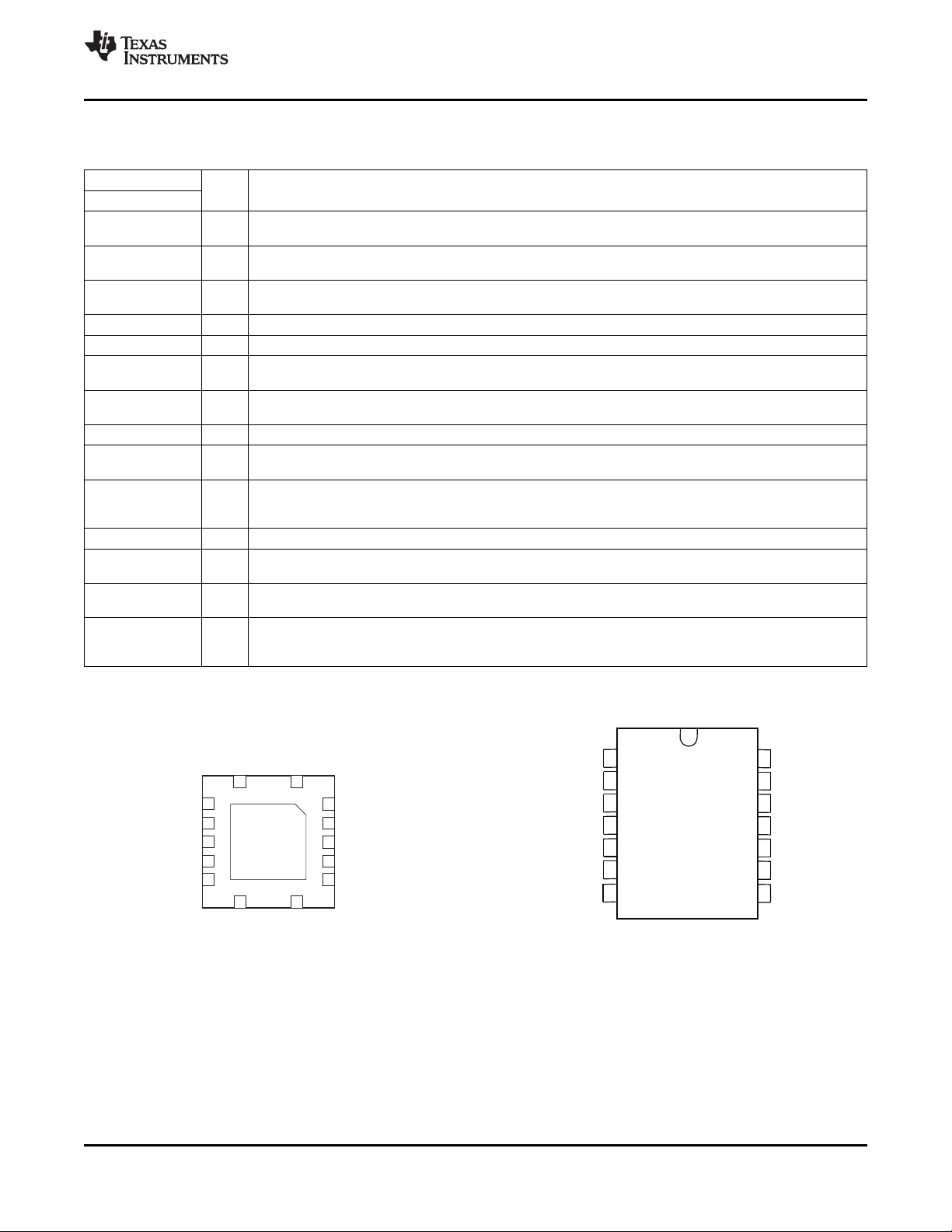
NAME NO.
DRVH 13 O
DRVL 9 O
EN_PSV 1 I
GND 7 I Signal ground pin.
LL 12 I/O High-side NFET gate driver return. Also serves as anode of overcurrent comparator.
PGND 8 I/O
PGOOD 6 O
TON 2 I On-time / frequency adjustment pin. Connect to LL with 100-kΩ to 600-kΩ resistor.
TRIP 11 I
VBST 14 I internal PN diode is connected between V5DRV to this pin. Designer can add external schottky diode if
VFB 5 I SMPS voltage feedback input. Connect the resistor divider here for adjustable output.
VOUT 3 I
V5DRV 10 I
V5FILT 4 I mV/μs or less and Tj< 85°C to secure safe start-up of the internal reference circuit. Apply RC filter consists of
...................................................................................................................................... SLVS631B –DECEMBER 2005–REVISED SEPTEMBER 2009
DEVICE INFORMATION
TERMINAL FUNCTIONS
TERMINAL
I/O DESCRIPTION
High-side NFET gate driver output. Source 5 Ω, sink 1.5 Ω LL-node referenced driver. Drive voltage
corresponds to VBST to LL voltage.
Rectifying (low-side) NFET gate driver output. Source 5 Ω, sink 1.5 Ω PGND referenced driver. Drive voltage
is V5DRV voltage.
Enable/power save pin. Connect to ground to disable SMPS. Connect to 3.3 V or 5 V to turn on SMPS and
activate skip mode. Float to turn on SMPS but disable skip mode (forced continuous conduction mode).
Ground return for rectifying NFET gate driver. Also cathode of overcurrent protection and source node of the
output discharge switch.
Power-good window comparator, open-drain, output. Pull up to 5-V rail with a pull-up resistor. Current
capability is 7.5 mA.
Overcurrent trip point set input. Connect resistor from this pin to signal ground to set threshold for both
overcurrent and negative overcurrent limit.
Supply input for high-side NFET gate driver (boost terminal). Connect capacitor from this pin to LL-node. An
forward drop is critical to drive the power NFET.
Connect to SMPS output. This terminal serves two functions: output voltage monitor for on-time adjustment,
and input for the output discharge switch.
5-V Power supply input for FET gate drivers. Internally connected to VBST by a PN diode. Connect 1 μF or
more between this pin and PGND to support instantaneous current for gate drivers.
5-V Power supply input for all the control circuitry except gate drivers. Supply 5-V ramp rate should be 17
300 Ω + 1 μF or 100 Ω + 4.7 μF at the pin input.
Copyright © 2005–2009, Texas Instruments Incorporated Submit Documentation Feedback 5
Product Folder Link(s) :TPS51117
2.9
3.9/3.6
48
TPS51117
SLVS631B –DECEMBER 2005–REVISED SEPTEMBER 2009......................................................................................................................................
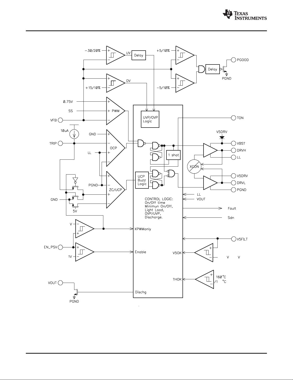
FUNCTIONAL BLOCK DIAGRAM
www.ti.com
DETAILED DESCRIPTION
PWM OPERATION
The main control loop of the TPS51117 is designed as an adaptive on-time pulse width modulation (PWM)
controller. It supports proprietary D-CAP™ Mode that uses an internal compensation circuit and is suitable for
minimal external component count configuration when an appropriate amount of ESR at the output capacitor(s) is
allowed. Basic operation of D-CAP Mode can be described as follows.
6 Submit Documentation Feedback Copyright © 2005–2009, Texas Instruments Incorporated
Product Folder Link(s) :TPS51117

V
OUT
+
ǒ
1 )
R
1
R
2
Ǔ
0.75 V
I
OUT(LL)
+
1
2 L ƒ
sw
ǒ
VIN* V
OUT
Ǔ
V
OUT
V
IN
TPS51117
www.ti.com
At the beginning of each cycle, the synchronous high-side MOSFET is turned on, or becomes ON state. This
MOSFET is turned off, or becomes OFF state, after the internal one shot timer expires. This one shot is
determined by VINand V
hence it is called adaptive on-time control or fixed frequency emulated on-time control (see PWM frequency and
Adaptive On-Time Control). The MOSFET is turned on again when both feedback information, monitored at V
voltage, indicates insufficient output voltage AND inductor current information indicates below the overcurrent
limit. Repeating the operation in this manner, the controller regulates the output voltage. The synchronous
low-side or rectifying MOSFET is turned on each OFF state to keep the conduction loss to a minimum.
The TPS51117 supports selectable PWM-only and auto-skip operation modes. If EN_PSV is grounded, the
switching regulator is disabled. If the EN_PSV pin is connected to 3.3 V or 5 V, the regulator is enabled with
auto-skip mode selected. The rectifying MOSFET is turned off when inductor current information detects zero
level. This enables a seamless transition to reduced frequency operation during a light load condition so that high
efficiency is maintained over a broad range of load currents. If the EN_PSV pin is floated, it is internally pulled up
to 1.95 V, and the regulator is enabled with PWM-only mode selected. The rectifying MOSFET is not turned off
when inductor current reaches zero. The converter runs forced continuous conduction mode for the entire load
range. System designers may want to use this mode to avoid a certain frequency during a light load condition but
with the cost of low efficiency. However, be aware the output has the capability to both source and sink current in
this mode. If the output terminal is connected to a voltage source higher than the regulator’s target, the converter
sinks current from the output and boosts the charge into the input capacitor. This may cause unexpected high
voltage at VIN and may damage the power FETs.
DC output voltage can be set by the external resistor divider as follows (refer to Figure 23, Figure 24, and
Figure 25).
...................................................................................................................................... SLVS631B –DECEMBER 2005–REVISED SEPTEMBER 2009
DETAILED DESCRIPTION (continued)
to keep the frequency fairly constant over the input voltage range at steady state,
OUT
FB
(1)
LIGHT LOAD CONDITION WITH AUTO-SKIP FUNCTION
If auto-skip mode is selected, the TPS51117 automatically reduces the switching frequency during a light load
condition to maintain high efficiency. This reduction of frequency is achieved smoothly and without an increase of
V
ripple or load regulation. Detailed operation is described as follows. As the output current decreases from a
out
heavy load condition, the inductor current is also reduced and eventually comes to the point that its valley
touches zero current, which is the boundary between continuous conduction and discontinuous conduction
modes. The rectifying MOSFET is turned off when this zero inductor current is detected. Since the output voltage
is still higher than the reference at this moment, both high-side and low-side MOSFETs are turned off and wait
for the next cycle. As the load current decreases further, the converter runs in discontinuous conduction mode,
taking longer time to discharge the output capacitor below the reference voltage. Note the ON time is kept the
same as during the heavy load condition. In reverse, when the output current increases from a light load to a
heavy load, the switching frequency increases to the preset value as the inductor current reaches to the
continuous conduction. The transition load point to light load operation, I
continuous and discontinuous conduction mode), can be calculated as follows:
where fswis the PWM switching frequency.
Switching frequency versus output current in the light load condition is a function of L, fsw, VINand V
decreases almost proportional to the output current from the I
at I
/5 if the PWM switching frequency is 300 kHz.
OUT(LL)
OUT(LL)
given above. For example, it is about 60 kHz
OUT(LL)
(i.e., the threshold between
(2)
, but it
OUT
Copyright © 2005–2009, Texas Instruments Incorporated Submit Documentation Feedback 7
Product Folder Link(s) :TPS51117
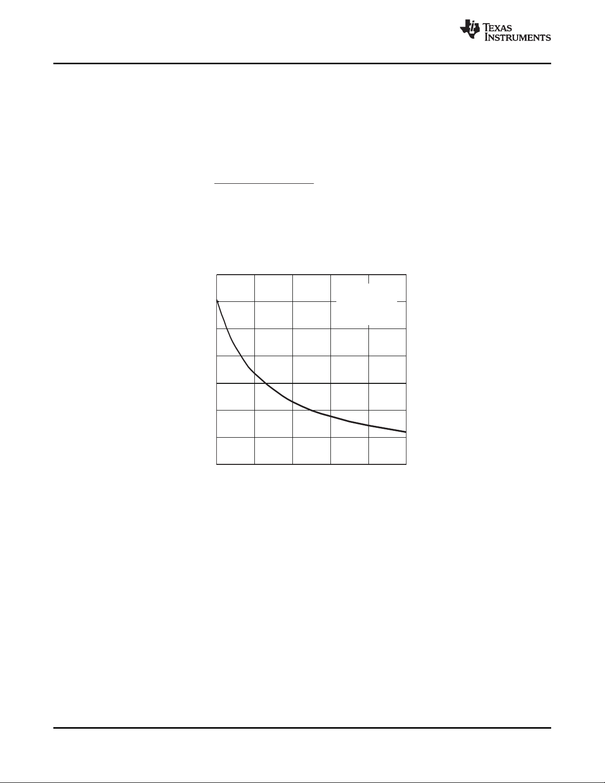
TON+ 19 10
*12
R
TON
ǒ
(2ń3)V
OUT
) 100 mV
V
IN
Ǔ
) 50 ns
0
100
200
300
400
500
600
f-Frequency-kHz
100
R -k
TON
W
400 500 600
700
200 300
V =15V,
V =2.5V,
PWM
IN
OUT
TPS51117
SLVS631B –DECEMBER 2005–REVISED SEPTEMBER 2009......................................................................................................................................
DETAILED DESCRIPTION (continued)
PWM FREQUENCY AND ADAPTIVE ON-TIME CONTROL
The TPS51117 employs an adaptive on-time control scheme and does not have a dedicated oscillator on board.
However, the device emulates a constant frequency by feed-forwarding the input and output voltages into the
on-time one-shot timer. The ON time is controlled inverse proportional to the input voltage, and proportional to
the output voltage, so that the duty ratio is kept as V
OUT/VIN
shows a simplified calculation of the on time.
Here, R
is the external resistor connected from TON pin to the LL node. In the equation, 19 pF represents the
TON
internal timing capacitor with some typical parasitic capacitance at the TON pin. Also, 50 nsec is the turn-off
delay time contributed by the internal circuit and that of the high-side MOSFET. Although this equation provides a
good approximation to start with, the accuracy depends on each design and selection of the high-side MOSFET.
Figure 1 shows the relationship of R
to the switching frequency.
TON
technically with the same cycle time. Equation 3
www.ti.com
(3)
The TPS51117 does not have a pin connected to VIN, but the input voltage information comes from the switch
node (LL node) during the ON state. An advantage of LL monitoring is that the loss in the high-side NFET is now
a part of the on-time calculation, thereby making the frequency more stable with load.
Another consideration about frequency is jitter. Jitter may be caused by many reasons, but the constant on-time
D-CAP mode scheme has some amount of inherent jitter. Since the output voltage ripple height is in the range of
a couple of tens of milli-volts. A milli-volt order of noise on the feedback signal can affect the frequency by a few
to ten percent. This is normal operation and has little harm to the power supply performance.
LOW-SIDE DRIVER
The low-side driver is designed to drive high-current, low R
represented by its internal resistance, which is 5 Ω for V5DRV to DRVL and 1.5 Ω for DRVL to PGND. A dead
time to prevent shoot through is internally generated between high-side MOSFET off to low-side MOSFET on,
and low-side MOSFET off to high-side MOSFET on. A 5-V bias voltage is delivered from V5DRV supply. The
average drive current is calculated by the FET gate charge at Vgs= 5 V times the switching frequency. The
instantaneous drive current is supplied by an input capacitor connected between V5DRV and GND.
8 Submit Documentation Feedback Copyright © 2005–2009, Texas Instruments Incorporated
Figure 1. Switching Frequency vs R
N-channel MOSFET(s). The drive capability is
DS(on)
Product Folder Link(s) :TPS51117
TON

V
TRIP
(mV) + R
TRIP
(kW) 10 (mA)
I
ocp
+ V
TRIPńRDS(on)
) I
ripple
ń2 +
V
TRIP
R
DS(on)
)
1
2 L ƒ
ǒ
VIN* V
OUT
Ǔ
V
OUT
V
IN
TPS51117
www.ti.com
HIGH-SIDE DRIVER
The high-side driver is designed to drive high-current, low R
floating driver, 5-V bias voltage is delivered from V5DRV supply. An internal PN diode is connected between
V5DRV to VBST. The designer can add an external schottky diode if forward drop is critical to drive the high-side
NFET or to achieve the last one percent efficiency improvement. The average drive current is also estimated by
the gate charge at Vgs= 5 V times the switching frequency. The instantaneous drive current is supplied by the
flying capacitor between the VBST pin and LL pin. The drive capability is represented by its internal resistance,
which is 5 Ω for VBST to DRVH and 1.5 Ω for DRVH to LL.
SOFTSTART
The TPS51117 has an internal, 1.2-ms, voltage servo softstart with overcurrent limit. When the EN_PSV pin
becomes high, an internal DAC begins ramping up the reference voltage to the error amplifier. Smooth control of
the output voltage is maintained during start up.
POWERGOOD
The TPS51117 has power-good output. PGOOD is an open drain 7.5-mA pull-down output. This pin should be
typically connected to a 5-V power supply node through a 100-kΩ resistor. The power-good function is activated
after the soft start has finished. If the output voltage becomes within ±5% of the target value, internal
comparators detect the power-good state and the power-good signal becomes high after a 64-μs internal delay. If
the output voltage goes outside ±10% of the target value, the power-good signal becomes low immediately.
...................................................................................................................................... SLVS631B –DECEMBER 2005–REVISED SEPTEMBER 2009
DETAILED DESCRIPTION (continued)
N-channel MOSFET(s). When configured as a
DS(on)
OUTPUT DISCHARGE CONTROL (SOFTSTOP)
The TPS51117 discharges output when EN_PSV is low or the converter is in a fault condition (UVP, OVP,
UVLO, or thermal shutdown). The TPS51117 discharges output using an internal 20-Ω MOSFET which is
connected to VOUT and PGND. The discharge time-constant is a function of the output capacitance and
resistance of the discharge transistor.
OVERCURRENT LIMIT
The TPS51117 has cycle-by-cycle overcurrent limiting control. Inductor current is monitored during the OFF state
and the controller keeps the OFF state when inductor current is larger than the overcurrent trip level. In order to
provide both good accuracy and a cost effective solution, the TPS51117 supports temperature compensated
MOSFET R
R
. The TRIP terminal sources 10-μA I
TRIP
the following equation.
Inductor current is monitored by the voltage between the PGND pin and the LL pin so the LL pin should be
connected to the drain terminal of the low-side MOSFET. I
compensate the temperature dependency of the R
PGND should be connected to the source terminal of the bottom MOSFET.
As the comparison is done during the OFF state, V
current at overcurrent threshold, I
In an overcurrent condition, the current to the load exceeds the current to the output capacitor thus the output
voltage tends to fall. Eventually it crosses the undervoltage protection threshold and shutdown.
sensing. The TRIP pin should be connected to GND through the trip voltage setting resistor,
DS(on)
, can be calculated as follows;
ocp
current, and the trip level is set to the OCL trip voltage, V
TRIP
has 4500 ppm/°C temperature coefficient to
TRIP
. PGND is used as the positive current sensing node so
DS(on)
sets the valley level of the inductor current. Thus, the load
TRIP
TRIP
as in
(4)
(5)
Copyright © 2005–2009, Texas Instruments Incorporated Submit Documentation Feedback 9
Product Folder Link(s) :TPS51117
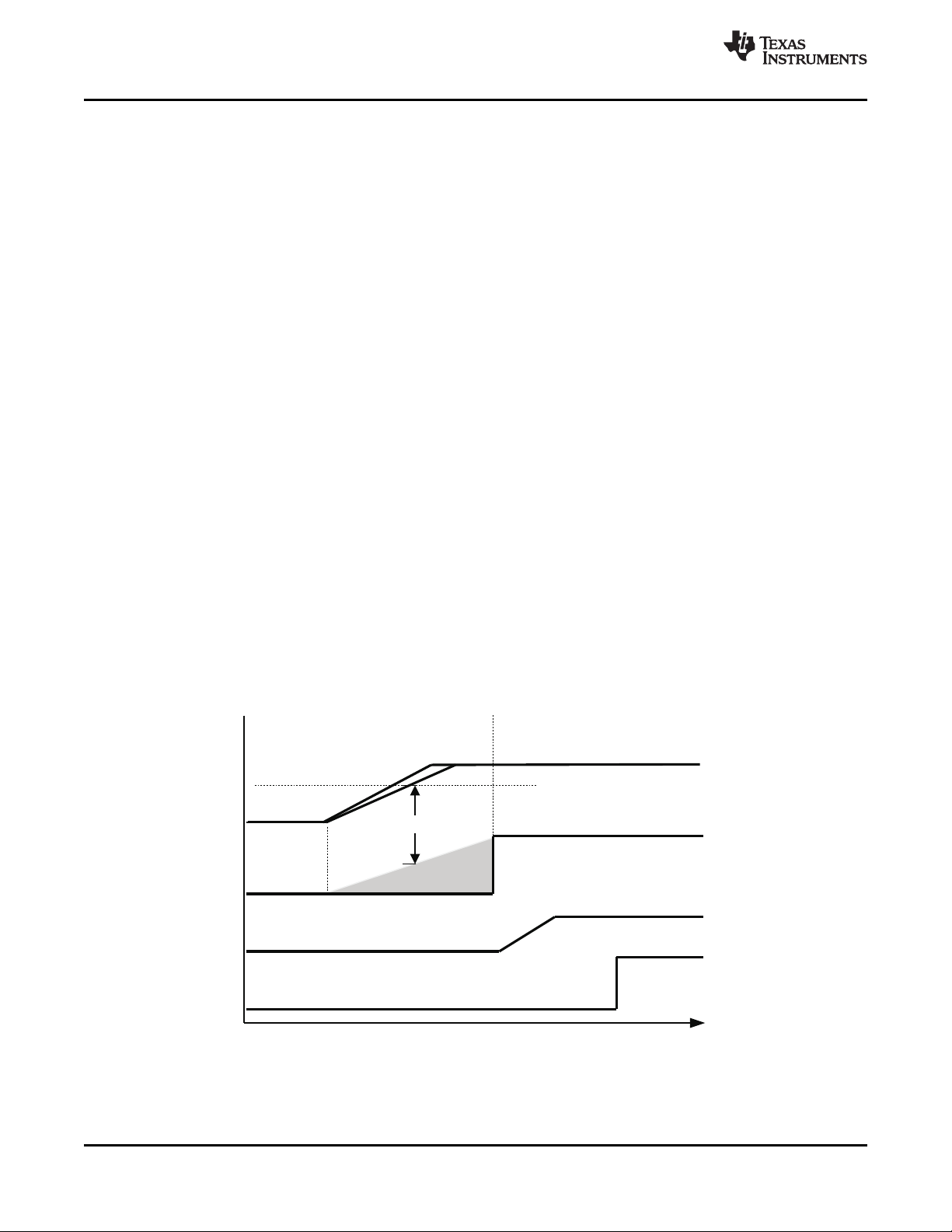
t – Time
UDG-09142
V5DRV
EN_PSV
VOUT
PGOOD
5V UVLO
V5FILT
TPS51117
SLVS631B –DECEMBER 2005–REVISED SEPTEMBER 2009......................................................................................................................................
DETAILED DESCRIPTION (continued)
NEGATIVE OVERCURRENT LIMIT (PWM-ONLY MODE)
The TPS51117 also supports cycle-by-cycle negative overcurrent limiting in PWM-only mode. The overcurrent
limit is set to be negative but is the same absolute value as the positive overcurrent limit. If output voltage
continues to rise, the bottom MOSFET stays on, thus inductor current is reduced and reverses direction after it
reaches zero. When there is too much negative current in the inductor, the bottom MOSFET is turned off and the
current flows to VIN through the body diode of the top MOSFET. Because this protection reduces current to
discharge the output capacitor, output voltage tends to rise, eventually hitting the overvoltage protection
threshold and shutdown. In order to prevent false OVP from triggering, the bottom MOSFET is turned on again
400 ns after it is turned off. If the device hits the negative overcurrent threshold again before output voltage is
discharged to the target level, the bottom MOSFET is turned off and the process repeats, which is called NOCL
Buzz. It ensures maximum allowable discharge capability when output voltage continues to rise. On the other
hand, if the output voltage is discharged to the target level before the NOCL threshold is reached, the bottom
MOSFET is turned off, the top MOSFET is then turned on, and the device resumes normal operation.
OVERVOLTAGE PROTECTION
The TPS51117 monitors a resistor divided feedback voltage to detect overvoltage and undervoltage condition.
When the feedback voltage becomes higher than 115% of the target value, the top MOSFET is turned off and
the bottom MOSFET is turned on immediately. The output is also discharged by the internal 20-Ω transistor.
Also, the TPS51117 monitors VOUT terminal voltage directly and if it becomes greater than 5.75 V, it turns off
the top MOSFET driver.
www.ti.com
UNDERVOLTAGE PROTECTION
When the feedback voltage becomes lower than 70% of the target value, the UVP comparator output goes high
and an internal UVP delay counter begins counting. After 32 μs, the TPS51117 latches off the high-side and
low-side MOSFETs and discharges the output with the internal 20-Ω transistor. This function is enabled after 2
ms from when EN_PSV is brought high, i.e., UVP is disabled during start up.
START UP SEQUENCE
Referring to Figure 2 which illustrates the timing sequence, to guarantee the proper startup the TPS51117,
always ensure that V
EN_PSV
is less or equal to that of V
V5FILT
prior to V
V5FILT
reaching V
UVLO
.
Figure 2. Startup Timing Sequence
10 Submit Documentation Feedback Copyright© 2005–2009, Texas Instruments Incorporated
Product Folder Link(s) :TPS51117

TPS51117
www.ti.com
UVLO PROTECTION
The TPS51117 has V5FILT undervoltage lockout protection (UVLO). When the V5FILT voltage is lower than the
UVLO threshold voltage, the TPS51117 is shut off. This is a nonlatched protection.
THERMAL SHUTDOWN
The TPS51117 monitors the temperature of itself. If the temperature exceeds the threshold value (typically
160°C), the TPS51117 shuts itself off. Both top and bottom gate drivers are tied low with output discharged
through the VOUT terminal. This is also a nonlatched protection. The device recovers once the temperature has
decreased approximately 12°C.
...................................................................................................................................... SLVS631B –DECEMBER 2005–REVISED SEPTEMBER 2009
DETAILED DESCRIPTION (continued)
Copyright © 2005–2009, Texas Instruments Incorporated Submit Documentation Feedback 11
Product Folder Link(s) :TPS51117

0
100
200
300
400
500
600
700
800
-50 0 50 100 150
T -JunctionTemperature- CJº
I -SupplyCurrent- A
V5FILTPWM
m
0
1
2
3
4
5
6
7
8
-50 0 50 100 150
T -JunctionTemperature- CJº
I -ShutdownCurrent- A
V5FILT_SHDN
m
4
6
8
10
12
14
16
-50 0 50 100
150
I -TRIP SourceCurrent- A
TRIP
m
T -JunctionTemperature- CJº
50
60
70
80
90
100
110
120
130
-50 0 50 100 150
OVP
UVP
T -JunctionTemperature- CJº
V ,V -OVP/UVP Threshold-%
OVP UVP
TPS51117
SLVS631B –DECEMBER 2005–REVISED SEPTEMBER 2009......................................................................................................................................
TYPICAL CHARACTERISTICS
www.ti.com
PWM SUPPLY CURRENT V5FILT SHUTDOWN CURRENT
JUNCTION TEMPERATURE JUNCTION TEMPERATURE
JUNCTION TEMPERATURE JUNCTION TEMPERATURE
vs vs
Figure 3. Figure 4.
TRIP CURRENT OVP/UVP THRESHOLD
vs vs
12 Submit Documentation Feedback Copyright© 2005–2009, Texas Instruments Incorporated
Figure 5. Figure 6.
Product Folder Link(s) :TPS51117

0
50
100
150
200
250
300
350
400
450
500
5 9 13 17 21 25
V =2.5V
O
V =1.05V
O
I =2 A,
PWMMode
O
f
sw
-SwitchingFrequency-kHz
V -InputVoltage-V
I
0
100
200
300
400
500
600
700
800
100 200 300 400 500 600 700
V =1.05V
O
V =2.5V
O
V =15V,
PWMMode
I
f
sw
-SwitchingFrequency-kHz
R -TONResistance-k
TON
W
0
50
100
150
200
250
300
350
400
450
0.001
0.010
0.1 1 10
f -SwitchingFrequency-kHz
sw
PWMOnly
AutoSkip
I -OutputCurrent- A
O
0
50
100
150
200
250
300
350
400
450
0.001 0.010 0.100 1.000 10.000
f -SwitchingFrequency-kHz
sw
PWMOnly
AutoSkip
I -OutputCurrent- A
O
www.ti.com
TPS51117
...................................................................................................................................... SLVS631B –DECEMBER 2005–REVISED SEPTEMBER 2009
TYPICAL CHARACTERISTICS (continued)
MEASURED SWITCHING FREQUENCY SWITCHING FREQUENCY
vs vs
TON RESISTANCE INPUT VOLTAGE
Figure 7. Figure 8.
SWITCHING FREQUENCY SWITCHING FREQUENCY
vs vs
OUTPUT CURRENT (1.05 V) OUTPUT CURRENT (2.5 V)
Copyright © 2005–2009, Texas Instruments Incorporated Submit Documentation Feedback 13
Figure 9. Figure 10.
Product Folder Link(s) :TPS51117

1.03
1.04
1.05
1.06
1.07
0 2 4 6 8 10
PWMOnly
AutoSkip
V -OutputVoltage-V
O
I -OutputCurrent- A
O
2.46
2.48
2.50
2.52
2.54
0 2 4 6 8 10
PWMOnly
AutoSkip
V -OutputVoltage-V
O
I -OutputCurrent- A
O
1.03
1.04
1.05
1.06
1.07
5 9 13 17 21 25
I =10 A
O
I =0 A
O
V -OutputVoltage-V
O
V -InputVoltage-V
I
AutoSkip
2.46
2.48
2.50
2.52
2.54
5 9 13 17 21 25
I =10 A
O
I =0 A
O
V -OutputVoltage-V
O
V -InputVoltage-V
I
AutoSkip
TPS51117
SLVS631B –DECEMBER 2005–REVISED SEPTEMBER 2009......................................................................................................................................
TYPICAL CHARACTERISTICS (continued)
1.05 V OUTPUT VOLTAGE 2.5 V OUTPUT VOLTAGE
vs vs
OUTPUT CURRENT OUTPUT CURRENT
www.ti.com
Figure 11. Figure 12.
1.05 V OUTPUT VOLTAGE 2.5 V OUTPUT VOLTAGE
vs vs
INPUT VOLTAGE INPUT VOLTAGE
Figure 13. Figure 14.
14 Submit Documentation Feedback Copyright© 2005–2009, Texas Instruments Incorporated
Product Folder Link(s) :TPS51117

0
10
20
30
40
50
60
70
80
90
100
0.001 0.01 0.1 1 10
h
-Efficiency-%
V =8V
I
V =12V
I
V =20V
I
V =8V
I
V =12V
I
V =20V
I
PWMOnly
f =350kHz
sw
AutoSkip
I -OutputCurrent- A
O
0
10
20
30
40
50
60
70
80
90
100
0.001 0.01 0.1 1 10
h
-Efficiency-%
V =20V
I
V =8V
I
V =12V
I
V =20V
I
V = 8 V
I
V =12V
I
PWMOnly
f =300kHz
sw
I -OutputCurrent- A
O
t-Time-10 s/divm
I (5 A/div)
IND
I (5 A/div)
O
V (50mV/div)
O
t-Time-10 s/divm
V (50mV/div)
O
I (5 A/div)
IND
I (5 A/div)
O
www.ti.com
TPS51117
...................................................................................................................................... SLVS631B –DECEMBER 2005–REVISED SEPTEMBER 2009
TYPICAL CHARACTERISTICS (continued)
1.05 V EFFICIENCY 2.5 V EFFICIENCY
vs vs
OUTPUT CURRENT OUTPUT CURRENT
Figure 15. Figure 16.
1.05 V LOAD TRANSIENT RESPONSE 2.5 V LOAD TRANSIENT RESPONSE
Copyright © 2005–2009, Texas Instruments Incorporated Submit Documentation Feedback 15
Figure 17. Figure 18.
Product Folder Link(s) :TPS51117

V (20mV/div)
O
LL (10V/div)
DRVL (5V/div)
EN_PSV(5V/div)
V (20mV/div)
O
LL (10V/div)
DRVL (5V/div)
EN_PSV(5V/div)
EN_PSV(2V/div)
V (1V/div)
O
PGOOD(5V/div)
t-Time-1ms/div
EN_PSV(2V/div)
V (1V/div)
O
PDOOD(5V/div)
DRVL (5V/div)
t-Time-10ms/div
TPS51117
SLVS631B –DECEMBER 2005–REVISED SEPTEMBER 2009......................................................................................................................................
TYPICAL CHARACTERISTICS (continued)
MODE TRANSITION MODE TRANSITION
AUTO-SKIP TO PWM PWM TO AUTO-SKIP
www.ti.com
Figure 19. Figure 20.
2.5 V START-UP WAVEFORMS 2.5 SHUTDOWN WAVEFORMS
Figure 21. Figure 22.
16 Submit Documentation Feedback Copyright © 2005–2009, Texas Instruments Incorporated
Product Folder Link(s) :TPS51117

Control
Logic
and
Driver
R1
R2
+
VFB
-
DRVL
I
L
VoltageDivider
PWM
VIN
Lx
DRVH
Io
Vc
Co
ESR
RL
Ic
SwitchingModulator
0.75V
+
OutputCapacitor
ƒ
o
+
1
2p ESR Co
v
ƒ
sw
4
R1 +
ǒ
V
OUT
* 0.75
Ǔ
0.75
R2
www.ti.com
...................................................................................................................................... SLVS631B –DECEMBER 2005–REVISED SEPTEMBER 2009
APPLICATION INFORMATION
LOOP COMPENSATION AND EXTERNAL PARTS SELECTION
D-CAP™ Mode Operation
A buck converter system using D-CAP™ Mode can be simplified as shown in Figure 23.
TPS51117
Figure 23. Simplified Diagram of the Modulator
The VFB voltage is compared with the internal reference voltage after the divider resistors. The PWM comparator
determines the timing to turn on the top MOSFET. The gain and speed of the comparator is high enough to keep
the voltage at the beginning of each on cycle (or the end of off cycle) substantially constant. The DC output
voltage may have line regulation due to ripple amplitude that slightly increases as the input voltage increases.
For loop stability, the 0 dB frequency, f0, defined in the follow equation must be lower than 1/4 of the switching
frequency.
(6)
As f0is determined solely by the output capacitor characteristics, loop stability of D-CAP™ Mode is determined
by capacitor chemistry. For example, specialty polymer capacitors (SP-CAP) have Co in the order of several 100
μF and ESR in range of 10 mΩ. These values make f0in the order of 100 kHz or less and the loop is stable.
However, ceramic capacitors have f0at more than 700 kHz, which is not suitable for this operational mode.
Although D-CAP™ Mode provides many advantages such as ease-of-use, minimum external component
configuration, and extremely short response time, due to not employing an error amplifier in the loop, a sufficient
feedback signal needs to be provided by an external circuit to reduce the jitter level. The required signal level is
approximately 15 mV at the comparing point. This generates V
ripple
= (V
/0.75) × 15 mV at the output node.
OUT
The output capacitor ESR should meet this requirement.
The external component selection is simple in D-CAP™ Mode:
1. Determine the value of R1 and R2
The recommended R2 value is 10 kΩ to 100 kΩ. Calculate R1 by Equation 7.
2. Choose R
TON
(7)
Copyright © 2005–2009, Texas Instruments Incorporated Submit Documentation Feedback 17
Product Folder Link(s) :TPS51117

T
ON(max)
+
1
ƒ
V
OUT
V
IN(min)
R
TON
+
3
2
ǒ
T
ON(max)
* 50 ns
Ǔ
19 10
*12
V
IN(min)
ǒ
V
OUT
) 150 mV
Ǔ
[W]
L
IND
+
1
I
IND(ripple)
ƒ
ǒ
V
IN(max)
* V
OUT
Ǔ
V
OUT
V
IN(max)
+
3
I
OUT(max)
ƒ
ǒ
V
IN(max)
* V
OUT
Ǔ
V
OUT
V
IN(max)
I
IND(peak)
+
V
TRIP
R
DS(on)
)
1
L ƒ
ǒ
V
IN(max)
* V
OUT
Ǔ
V
OUT
V
IN(max)
ESR +
V
OUT
0.015
I
ripple
0.75
[
V
OUT
I
OUT(max)
60 [mW]
30 mV
1.2 I
OUT(max)
* 0.5 I
ripple
v R
DS(on)
v
200 mV
1.2 I
OUT(max)
* 0.5 I
ripple
TPS51117
SLVS631B –DECEMBER 2005–REVISED SEPTEMBER 2009......................................................................................................................................
Switching frequency is usually determined by the overall view of the DC-DC converter design of: size,
efficiency or cost, and mostly dictated by external component constraints such as the size of inductor and/or
output capacitor. In the case where an extremely low or high duty factor is expected, the minimum on-time or
off-time also needs to be considered to satisfy the required duty factor. Once the switching frequency is
decided, R
3. Choose inductor
A good starting point inductance value is where the ripple current is approximately 1/4 to 1/2 of the maximum
output current.
For applications that require fast transient response with minimum V
inductance than above. The cost of a small inductance value is higher steady state ripple, larger line
regulation, and higher switching loss.
The inductor also needs to have low DCR to achieve good efficiency, as well as enough room above peak
inductor current before saturation. The peak inductor current can be estimated as follows.
can be determined by Equation 8 and Equation 9,
TON
overshoot, consider a smaller
OUT
www.ti.com
(8)
(9)
(10)
4. Choose output capacitor(s)
Organic semiconductor capacitor(s) or specialty polymer capacitor(s) are recommended. Determine ESR to
meet the required ripple voltage above. A quick approximation is shown in Equation 12.
5. Choose MOSFETs
Loss-less current sensing and overcurrent protection of the TPS51117 is determined by R
low-side MOSFET. So, R
range of 30 mV to 200 mV for the entire operational temperature range. Assuming a 20% guard band, R
in the following equation should satisfy the full temperature range.
6. Choose R
Once the low-side FET is decided, select an appropriate R
I
peak
7. LPF for V5FILT
In order to reject high frequency noise and also secure safe start-up of the internal reference circuit, apply
1 μF of MLCC closely at the V5FILT pin with a 300-Ω resistor to create a LPF between +5-V supply and the
pin.
8. VBST capacitor, VBST diode
trip
.
times the inductor current value at the overcurrent point should be in the
DS(on)
value that provides V
trip
equal to R
trip
DS(on)
DS(on)
(11)
(12)
of the
DS(on)
(13)
times
18 Submit Documentation Feedback Copyright © 2005–2009, Texas Instruments Incorporated
Product Folder Link(s) :TPS51117

IG+ Qg ƒ
sw
W
DRIVE
+ V
V5DRV
ǒ
Q
g(top)
) Q
g(btm)
Ǔ
ƒ
sw
W
PKG
+
T
J(max)
* T
A(max)
q
JA
TPS51117
www.ti.com
THERMAL CONSIDERATION
Power dissipation of the TPS51117 is mainly generated from the FET drivers. Average drive current can be
estimated by gate charge, Qg, times the switching frequency.
Qgis the charge needed to charge gate capacitance up to the V5DRV voltage of 5 V. Actual values are shown
on MOSFET datasheets provided by the manufacturer. Total power dissipation, therefore, to drive the top and
bottom MOSFETs can be calculated by the following equation Equation 15.
This power plus a small amount of dissipation (less than 5 mW) from controller circuitry needs to be effectively
dissipated from the package. Maximum power dissipation allowed for the package is calculated by:
...................................................................................................................................... SLVS631B –DECEMBER 2005–REVISED SEPTEMBER 2009
Apply 0.1-μF MLCC between VBST and the LL node as the flying capacitor for the high-side FET driver. The
TPS51117 has its own boost diode on-board between V5DRV and VBST. This is a PN junction diode and
strong enough for most typical applications. However, in case efficiency has priority over cost, the designer
may add a Schottky diode externally to improve gate drive voltage of the high-side FET. A Schottky diode
has a higher leakage current, especially at high temperature, than a PN junction diode. A low leakage diode
should be selected in order to maintain VBST voltage during low frequency operation in skip mode.
(14)
(15)
(16)
Where
• T
• T
• θJAis the thermal resistance from the silicon junction to the ambient
This thermal resistance strongly depends on board layout. The TPS51117 is assembled in a standard TSSOP
package and the heat mainly moves to the board through its leads.
is 125°C
J(max)
is the maximum ambient temperature in the system
A(max)
LAYOUT CONSIDERATIONS
Certain points must be considered before starting a layout work using the TPS51117.
• Connect the RC low-pass filter from 5-V supply to V5FILT, 300 Ω and 1 μF are recommended. Place the filter
capacitor close to the device, within 12 mm (0.5 inches) if possible.
• Connect the overcurrent setting resistors from TRIP to GND close to the device, right next to the device, if
possible. The trace from TRIP to resistor and resistor to GND should avoid coupling to a high voltage
switching node.
• The discharge path (VOUT) should have a dedicated trace to the output capacitor(s); separate from the
output voltage sensing trace, and use a 1,5 mm (60 mils) or wider trace with no loops. Make sure the
feedback current setting resistor (the resistor between VFB to GND) is tied close to the device GND. The
trace from this resistor to the VFB pin should be short and thin. Place on the component side and avoid vias
between this resistor and the device.
• Connections from the drivers to the respective gate of the high-side or the low-side MOSFET should be as
short as possible to reduce stray inductance. Use a 0.65 mm (25 mils) or wider trace.
• All sensitive analog traces and components such as VOUT, VFB, GND, EN_PSV, PGOOD, TRIP, V5FILT,
and TON should be placed away from high-voltage switching nodes such as LL, DRVL, DRVH or VBST to
avoid coupling. Use internal layer(s) as ground plane(s) and shield feedback trace from power traces and
components.
• Gather the ground terminals of the VINcapacitor(s), V
MOSFETs as close as possible. GND (signal ground) and PGND (power ground) should be connected
strongly together near the device. The PCB trace defined as LL node, which connects to the source of the
high-side MOSFET, the drain of the low-side MOSFET, and the high-voltage side of the inductor, should be
as short and wide as possible.
capacitor(s), and the source of the low-side
OUT
Copyright © 2005–2009, Texas Instruments Incorporated Submit Documentation Feedback 19
Product Folder Link(s) :TPS51117

1
2
3
14
13
12
VBST
DRVH
LL
EN_PSV
TON
VOUT
TPS51117PW
4
5
6
7
11
10
9
8
TRIP
V5DRV
DRVL
PGND
V5FILT
VFB
PGOOD
GND
+
VO
1.05V/10A
Q2
L1
1.0 Hm
Q1
-
PGND
C2
2 0 Fm
C1A C1B
R6
100k
W
PGOOD
+5V
EN_PSV
R4
R1
8.5k
W
R2
22k
W
R3
249k
W
R5
300
W
+VBAT
C3
1 Fm
GND
+
+
C4
0.1 Fm
GND
TPS51117RGY
+
VO
1.05V/10A
Q2
L1
1.0 Hm
Q1
-
PGND
C2
20 Fm
C1A
GND
C4
0.1 Fm
C1B
R6
100kW
PGOOD
+5V
EN_PSV
R4
R1
8.5kW
R2
22kW
R3
249kW
R5
300W
+VBAT
C3
1 Fm
GND
+
+
1
2
3
14
13
12
VBST
DRVH
LL
EN_PSV
TON
VOUT
4
5
6
7
11
10
9
8
TRIP
V5DRV
DRVL
PGND
V5FILT
VFB
PGOOD
GND
TPS51117
SLVS631B –DECEMBER 2005–REVISED SEPTEMBER 2009......................................................................................................................................
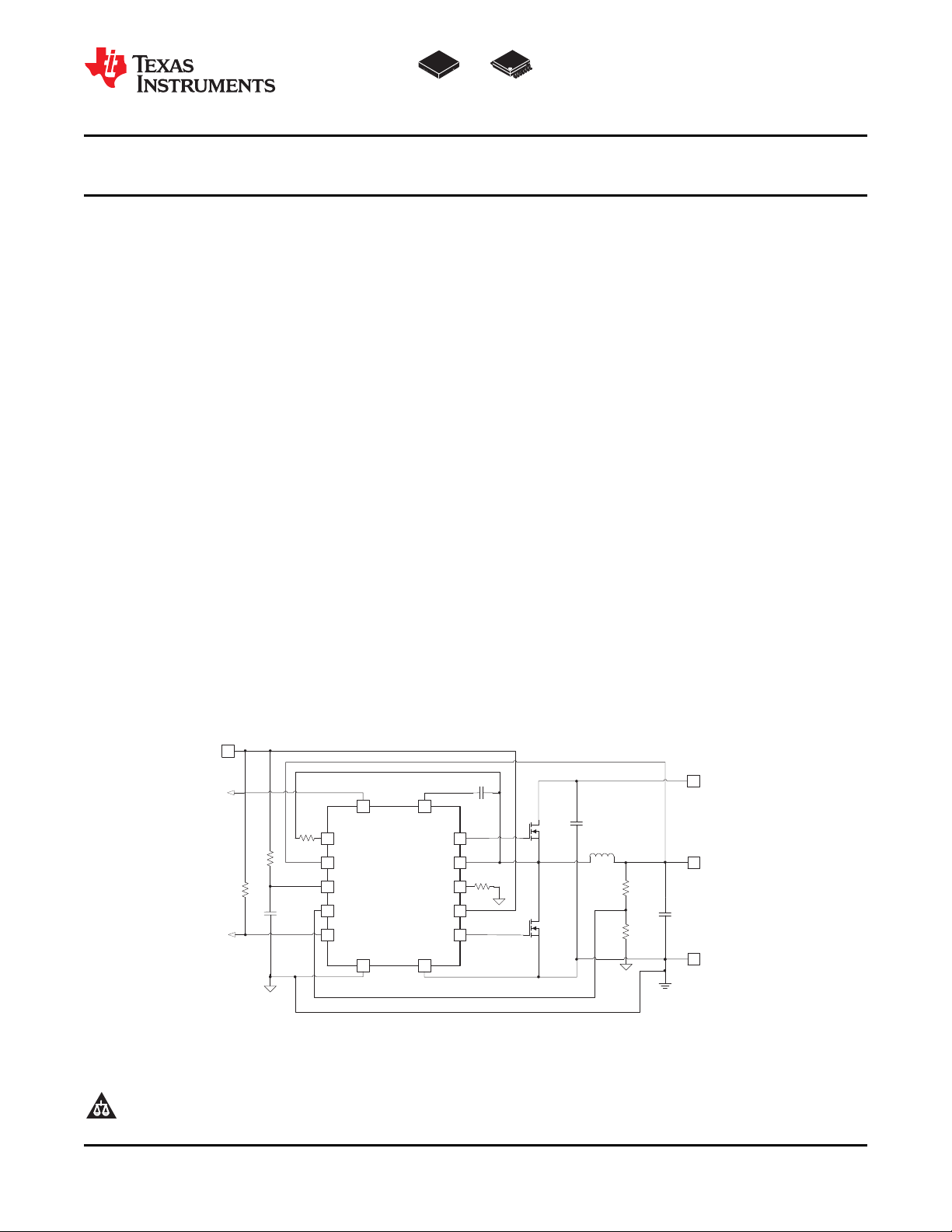
Figure 24. 1.05-V/10-A Application From VBAT (PW Package)
www.ti.com
Figure 25. 1.05-V/10-A Application From VBAT (RGY Package)
Table 1. Typical Application Circuit Components
20 Submit Documentation Feedback Copyright © 2005–2009, Texas Instruments Incorporated
SYMBOL SPECIFICATION MANUFACTURER PART NUMBER
C1A, C1B 470 μF, 2.5 V, 12 mΩ SANYO 2R5TPE470MC
C2 10 μF, 25 V, 2 pcs Murata GRM31CR61E106KA12B
L1 1.0 μH Vishay, Toko IHLP-5050, FDA1254-1R0M
Q1 30V, 13 mΩ International Rectifier IRF7821
Q2 30 V, 5.8 mΩ International Rectifier IRF8113
R4 8.06 kΩ — Std
Product Folder Link(s) :TPS51117

TPS51117
www.ti.com
NOTE: Page numbers for previous revisions may differ from page numbers in the current version.
Changes from Revision A (June, 2009) to Revision B ................................................................................................... Page
• Added Start Up Sequence section ...................................................................................................................................... 10
• Added Start Up Timing Sequence diagram ........................................................................................................................ 10
...................................................................................................................................... SLVS631B –DECEMBER 2005–REVISED SEPTEMBER 2009
REVISION HISTORY
Copyright © 2005–2009, Texas Instruments Incorporated Submit Documentation Feedback 21
Product Folder Link(s) :TPS51117

PACKAGE OPTION ADDENDUM
www.ti.com 8-Dec-2009
PACKAGING INFORMATION
Orderable Device Status
(1)
Package
Type
Package
Drawing
Pins Package
Qty
Eco Plan
TPS51117PW ACTIVE TSSOP PW 14 90 Green (RoHS &
(2)
Lead/Ball Finish MSL Peak Temp
CU NIPDAU Level-1-260C-UNLIM
(3)
no Sb/Br)
TPS51117PWG4 ACTIVE TSSOP PW 14 90 Green (RoHS &
CU NIPDAU Level-1-260C-UNLIM
no Sb/Br)
TPS51117PWR ACTIVE TSSOP PW 14 2000 Green (RoHS &
CU NIPDAU Level-1-260C-UNLIM
no Sb/Br)
TPS51117PWRG4 ACTIVE TSSOP PW 14 2000 Green (RoHS &
CU NIPDAU Level-1-260C-UNLIM
no Sb/Br)
TPS51117RGYR ACTIVE VQFN RGY 14 3000 Green (RoHS &
CU NIPDAU Level-2-260C-1 YEAR
no Sb/Br)
TPS51117RGYRG4 ACTIVE VQFN RGY 14 3000 Green (RoHS &
CU NIPDAU Level-2-260C-1 YEAR
no Sb/Br)
TPS51117RGYT ACTIVE VQFN RGY 14 250 Green (RoHS &
CU NIPDAU Level-2-260C-1 YEAR
no Sb/Br)
TPS51117RGYTG4 ACTIVE VQFN RGY 14 250 Green (RoHS &
CU NIPDAU Level-2-260C-1 YEAR
no Sb/Br)
(1)
The marketing status values are defined as follows:
ACTIVE: Product device recommended for new designs.
LIFEBUY: TI has announced that the device will be discontinued, and a lifetime-buy period is in effect.
NRND: Not recommended for new designs. Device is in production to support existing customers, but TI does not recommend using this part in
a new design.
PREVIEW: Device has been announced but is not in production. Samples may or may not be available.
OBSOLETE: TI has discontinued the production of the device.
(2)
Eco Plan - The planned eco-friendly classification: Pb-Free (RoHS), Pb-Free (RoHS Exempt), or Green (RoHS & no Sb/Br) - please check
http://www.ti.com/productcontent for the latest availability information and additional product content details.
TBD: The Pb-Free/Green conversion plan has not been defined.
Pb-Free (RoHS): TI's terms "Lead-Free" or "Pb-Free" mean semiconductor products that are compatible with the current RoHS requirements
for all 6 substances, including the requirement that lead not exceed 0.1% by weight in homogeneous materials. Where designed to be soldered
at high temperatures, TI Pb-Free products are suitable for use in specified lead-free processes.
Pb-Free (RoHS Exempt): This component has a RoHS exemption for either 1) lead-based flip-chip solder bumps used between the die and
package, or 2) lead-based die adhesive used between the die and leadframe. The component is otherwise considered Pb-Free (RoHS
compatible) as defined above.
Green (RoHS & no Sb/Br): TI defines "Green" to mean Pb-Free (RoHS compatible), and free of Bromine (Br) and Antimony (Sb) based flame
retardants (Br or Sb do not exceed 0.1% by weight in homogeneous material)
(3)
MSL, Peak Temp. -- The Moisture Sensitivity Level rating according to the JEDEC industry standard classifications, and peak solder
temperature.
Important Information and Disclaimer:The information provided on this page represents TI's knowledge and belief as of the date that it is
provided. TI bases its knowledge and belief on information provided by third parties, and makes no representation or warranty as to the
accuracy of such information. Efforts are underway to better integrate information from third parties. TI has taken and continues to take
reasonable steps to provide representative and accurate information but may not have conducted destructive testing or chemical analysis on
incoming materials and chemicals. TI and TI suppliers consider certain information to be proprietary, and thus CAS numbers and other limited
information may not be available for release.
In no event shall TI's liability arising out of such information exceed the total purchase price of the TI part(s) at issue in this document sold by TI
to Customer on an annual basis.
Addendum-Page 1

PACKAGE MATERIALS INFORMATION
www.ti.com 29-Nov-2012
TAPE AND REEL INFORMATION
*All dimensions are nominal
Device Package
TPS51117PWR TSSOP PW 14 2000 330.0 12.4 6.9 5.6 1.6 8.0 12.0 Q1
TPS51117RGYR VQFN RGY 14 3000 330.0 12.4 3.75 3.75 1.15 8.0 12.0 Q1
TPS51117RGYT VQFN RGY 14 250 180.0 12.4 3.75 3.75 1.15 8.0 12.0 Q1
TPS51117RGYT VQFN RGY 14 250 180.0 12.4 3.75 3.75 1.15 8.0 12.0 Q1
Type
Package
Drawing
Pins SPQ Reel
Diameter
(mm)
Reel
Width
W1 (mm)
A0
(mm)B0(mm)K0(mm)P1(mm)W(mm)
Pin1
Quadrant
Pack Materials-Page 1

PACKAGE MATERIALS INFORMATION
www.ti.com 29-Nov-2012
*All dimensions are nominal
Device Package Type Package Drawing Pins SPQ Length (mm) Width (mm) Height (mm)
TPS51117PWR TSSOP PW 14 2000 367.0 367.0 35.0
TPS51117RGYR VQFN RGY 14 3000 367.0 367.0 35.0
TPS51117RGYT VQFN RGY 14 250 210.0 185.0 35.0
TPS51117RGYT VQFN RGY 14 250 210.0 185.0 35.0
Pack Materials-Page 2


IMPORTANT NOTICE
Texas Instruments Incorporated and its subsidiaries (TI) reserve the right to make corrections, enhancements, improvements and other
changes to its semiconductor products and services per JESD46, latest issue, and to discontinue any product or service per JESD48, latest
issue. Buyers should obtain the latest relevant information before placing orders and should verify that such information is current and
complete. All semiconductor products (also referred to herein as “components”) are sold subject to TI’s terms and conditions of sale
supplied at the time of order acknowledgment.
TI warrants performance of its components to the specifications applicable at the time of sale, in accordance with the warranty in TI’s terms
and conditions of sale of semiconductor products. Testing and other quality control techniques are used to the extent TI deems necessary
to support this warranty. Except where mandated by applicable law, testing of all parameters of each component is not necessarily
performed.
TI assumes no liability for applications assistance or the design of Buyers’ products. Buyers are responsible for their products and
applications using TI components. To minimize the risks associated with Buyers’ products and applications, Buyers should provide
adequate design and operating safeguards.
TI does not warrant or represent that any license, either express or implied, is granted under any patent right, copyright, mask work right, or
other intellectual property right relating to any combination, machine, or process in which TI components or services are used. Information
published by TI regarding third-party products or services does not constitute a license to use such products or services or a warranty or
endorsement thereof. Use of such information may require a license from a third party under the patents or other intellectual property of the
third party, or a license from TI under the patents or other intellectual property of TI.
Reproduction of significant portions of TI information in TI data books or data sheets is permissible only if reproduction is without alteration
and is accompanied by all associated warranties, conditions, limitations, and notices. TI is not responsible or liable for such altered
documentation. Information of third parties may be subject to additional restrictions.
Resale of TI components or services with statements different from or beyond the parameters stated by TI for that component or service
voids all express and any implied warranties for the associated TI component or service and is an unfair and deceptive business practice.
TI is not responsible or liable for any such statements.
Buyer acknowledges and agrees that it is solely responsible for compliance with all legal, regulatory and safety-related requirements
concerning its products, and any use of TI components in its applications, notwithstanding any applications-related information or support
that may be provided by TI. Buyer represents and agrees that it has all the necessary expertise to create and implement safeguards which
anticipate dangerous consequences of failures, monitor failures and their consequences, lessen the likelihood of failures that might cause
harm and take appropriate remedial actions. Buyer will fully indemnify TI and its representatives against any damages arising out of the use
of any TI components in safety-critical applications.
In some cases, TI components may be promoted specifically to facilitate safety-related applications. With such components, TI’s goal is to
help enable customers to design and create their own end-product solutions that meet applicable functional safety standards and
requirements. Nonetheless, such components are subject to these terms.
No TI components are authorized for use in FDA Class III (or similar life-critical medical equipment) unless authorized officers of the parties
have executed a special agreement specifically governing such use.
Only those TI components which TI has specifically designated as military grade or “enhanced plastic” are designed and intended for use in
military/aerospace applications or environments. Buyer acknowledges and agrees that any military or aerospace use of TI components
which have not been so designated is solely at the Buyer's risk, and that Buyer is solely responsible for compliance with all legal and
regulatory requirements in connection with such use.
TI has specifically designated certain components as meeting ISO/TS16949 requirements, mainly for automotive use. In any case of use of
non-designated products, TI will not be responsible for any failure to meet ISO/TS16949.
Products Applications
Audio www.ti.com/audio Automotive and Transportation www.ti.com/automotive
Amplifiers amplifier.ti.com Communications and Telecom www.ti.com/communications
Data Converters dataconverter.ti.com Computers and Peripherals www.ti.com/computers
DLP® Products www.dlp.com Consumer Electronics www.ti.com/consumer-apps
DSP dsp.ti.com Energy and Lighting www.ti.com/energy
Clocks and Timers www.ti.com/clocks Industrial www.ti.com/industrial
Interface interface.ti.com Medical www.ti.com/medical
Logic logic.ti.com Security www.ti.com/security
Power Mgmt power.ti.com Space, Avionics and Defense www.ti.com/space-avionics-defense
Microcontrollers microcontroller.ti.com Video and Imaging www.ti.com/video
RFID www.ti-rfid.com
OMAP Applications Processors www.ti.com/omap TI E2E Community e2e.ti.com
Wireless Connectivity www.ti.com/wirelessconnectivity
Mailing Address: Texas Instruments, Post Office Box 655303, Dallas, Texas 75265
Copyright © 2012, Texas Instruments Incorporated

 Loading...