

Page 1
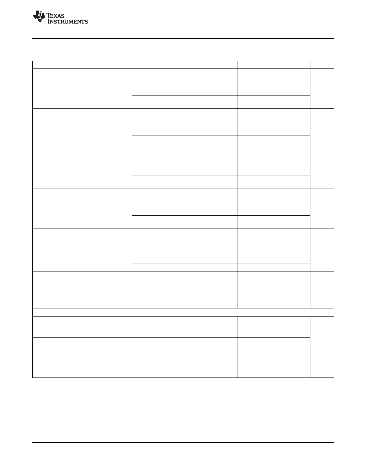
S5
PGOOD
VREF
0.9 V
10 mA
VTT
0.9 V
2 A
TPS51116RGE
20 19
18
17
VBST DRVH LL DRVL
V5FILT
VLDOIN
VTTGND
VTTSNS
7 8
VTT
CS_GND
9 10
VDDQSET
CS
VDDQSNS
16
15
14
13PGOOD
1211
S5S3
GND
MODE
VTTREF
COMP
NC NC
V5IN
PGND
22 2124 23
1
2
3
4
5
6
C1
5V_IN
VDDQ
1.8 V
10 A
VIN
M1
M2
S3
L1
IRF7832
IRF7821
C4
C3
Ceramic
2y10 µF
Ceramic
0.033 µF
Ceramic
0.1 µF
1 µH
C6
SP−CAP
2y150 µF
C5
Ceramic
2y10 µF
C2
Ceramic
1 µF
C7
Ceramic
1 µF
R2
100 kΩ
R1
5.1 kΩ
R3
5.1 Ω
UDG−04153
TI Information — Selective Disclosure
TPS51116
www.ti.com
Complete DDR, DDR2, DDR3, and LPDDR3 Memory Power Solution
Synchronous Buck Controller, 3-A LDO, Buffered Reference
Check for Samples: TPS51116
1
FEATURES
2
• Synchronous Buck Controller (VDDQ)
– Wide-Input Voltage Range: 3.0-V to 28-V
– D−CAP™ Mode with 100-ns Load Step
Response
– Current Mode Option Supports Ceramic
Output Capacitors
– Supports Soft-Off in S4/S5 States
– Current Sensing from R
– 2.5-V (DDR), 1.8-V (DDR2), Adjustable to
1.5-V (DDR3) or 1.2-V (LPDDR3) or
Output Range 0.75-V to 3.0-V
– Equipped with Powergood, Overvoltage
Protection and Undervoltage Protection
• 3-A LDO (VTT), Buffered Reference (VREF)
– Capable to Sink and Source 3 A
– LDO Input Available to Optimize Power
Losses
– Requires only 20-μF Ceramic Output
Capacitor
– Buffered Low Noise 10-mA VREF Output
– Accuracy ±20 mV for both VREF and VTT
– Supports High-Z in S3 and Soft-Off in S4/S5
– Thermal Shutdown
DS(on)
or Resistor
SLUS609I –MAY 2004–REVISED JANUARY 2014
DESCRIPTION
The TPS51116 provides a complete power supply for
DDR/SSTL-2, DDR2/SSTL-18, DDR3/SSTL-15, and
LPDDR3 memory systems. It integrates a
synchronous buck controller with a 3-A sink/source
tracking linear regulator and buffered low noise
reference. The TPS51116 offers the lowest total
solution cost in systems where space is at a
premium. The TPS51116 synchronous controller runs
fixed 400-kHz, pseudo-constant frequency PWM with
an adaptive on-time control that can be configured in
D-CAP™ Mode for ease of use and fastest transient
response or in current mode to support ceramic
output capacitors. The 3-A sink/source LDO
maintains fast transient response only requiring 20-μF
(2 × 10 μF) of ceramic output capacitance. In
addition, the LDO supply input is available externally
to significantly reduce the total power losses. The
TPS51116 supports all of the sleep state controls
placing VTT at high-Z in S3 (suspend to RAM) and
discharging VDDQ, VTT and VTTREF (soft-off) in
S4/S5 (suspend to disk). TPS51116 has all of the
protection features including thermal shutdown and is
offered in both a 20-pin HTSSOP PowerPAD™
package and 24-pin 4×4 QFN.
APPLICATIONS
• DDR/DDR2/DDR3/LPDDR3 Memory Power
Supplies
• SSTL-2, SSTL-18, SSTL-15 and HSTL
Termination
Copyright © 2004–2014, Texas Instruments Incorporated
1
Please be aware that an important notice concerning availability, standard warranty, and use in critical applications of
Texas Instruments semiconductor products and disclaimers thereto appears at the end of this data sheet.
2D-CAP, PowerPAD are trademarks of Texas Instruments.
PRODUCTION DATA information is current as of publication date.
Products conform to specifications per the terms of the Texas
Instruments standard warranty. Production processing does not
necessarily include testing of all parameters.
Page 2
TPS51116
TI Information — Selective Disclosure
SLUS609I –MAY 2004–REVISED JANUARY 2014
This integrated circuit can be damaged by ESD. Texas Instruments recommends that all integrated circuits be handled with
appropriate precautions. Failure to observe proper handling and installation procedures can cause damage.
ESD damage can range from subtle performance degradation to complete device failure. Precision integrated circuits may be more
susceptible to damage because very small parametric changes could cause the device not to meet its published specifications.
ORDERING INFORMATION
T
A
-40°C to 85°C
(1) All packaging options have Cu NIPDAU lead/ball finish.
ABSOLUTE MAXIMUM RATINGS
PACKAGE PINS ORDER
Plastic HTSSOP
PowerPAD (PWP)
Plastic QUAD Flat Pack TPS51116RGER 3000
(QFN)
(1)
ORDERABLE PART OUTPUT
TPS51116PWPRG4 Tape-and-reel 2000
(1)
NUMBER SUPPLY
TPS51116PWP Tube 70
TPS51116PWPR 20 Tape-and-reel 2000
TPS51116RGE Tube 90
24 tape-and-reel
TPS51116RGET 250
Large
Small
tape-and-reel
www.ti.com
MINIMUM
QUANTITY
over operating free-air temperature range unless otherwise noted
MIN MAX UNIT
VBST –0.3 36
VBST wrt LL –0.3 6
V
V
T
T
(1) Stresses beyond those listed under "absolute maximum ratings" may cause permanent damage to the device. These are stress ratings
Input voltage range V
IN
Output voltage range LL –1.0 30 V
OUT
Operating ambient temperature range –40 85
A
Storage temperature –55 150
stg
only, and functional operation of the device at these or any other conditions beyond those indicated under "recommended operating
conditions" is not implied. Exposure to absolute-maximum-rated conditions for extended periods may affect device reliability. All voltage
values are with respect to the network ground terminal unless otherwise noted.
CS, MODE, S3, S5, VTTSNS, VDDQSNS, V5IN, VLDOIN, VDDQSET,
V5FILT
PGND, VTTGND, CS_GND –0.3 0.3
DRVH –1.0 36
COMP, DRVL, PGOOD, VTT, VTTREF –0.3 6
–0.3 6
°C
DISSIPATION RATINGS
PACKAGE TA= 25°C
20-pin PWP 2.53 25.3 1.01
24-pin RGE 2.20 22.0 0.88
2 Submit Documentation Feedback Copyright © 2004–2014, Texas Instruments Incorporated
TA< 25°C POWER RATING TA= 85°C POWER RATING
(W) (W)
Product Folder Links: TPS51116
DERATING FACTOR ABOVE
(mW/°C)
Page 3
TI Information — Selective Disclosure
TPS51116
www.ti.com
SLUS609I –MAY 2004–REVISED JANUARY 2014
RECOMMENDED OPERATING CONDITIONS
MIN MAX UNIT
Supply voltage, V5IN, V5FILT 4.75 5.25 V
VBST, DRVH –0.1 34
LL –0.6 28
VLDOIN, VTT, VTTSNS, VDDQSNS –0.1 3.6
Voltage range V
Operating free-air temperature, T
A
VTTREF –0.1 1.8
PGND, VTTGND, CS_GND –0.1 0.1
S3, S5, MODE, VDDQSET, CS, COMP, PGOOD,
DRVL
–0.1 5.25
–40 85 °C
Copyright © 2004–2014, Texas Instruments Incorporated Submit Documentation Feedback 3
Product Folder Links: TPS51116
Page 4
TPS51116
TI Information — Selective Disclosure
SLUS609I –MAY 2004–REVISED JANUARY 2014
ELECTRICAL CHARACTERISTICS
over operating free-air temperature range, V
PARAMETER TEST CONDITIONS MIN TYP MAX UNIT
SUPPLY CURRENT
TA= 25°C, No load, VS3= VS5= 5 V,
I
V5IN1
I
V5IN2
I
V5IN3
I
V5INSDN
I
VLDOIN1
I
VLDOIN2
I
VLDOINSDN
Supply current 1, V5IN
Supply current 2, V5IN
Supply current 3, V5IN
Shutdown current, V5IN
Supply current 1, VLDOIN TA= 25°C, No load, VS3= VS5= 5 V 1 10
Supply current 2, VLDOIN TA= 25°C, No load, VS3= 5 V, VS5= 0 V, 0.1 10
Standby current, VLDOIN TA= 25°C, No load, VS3= VS5= 0 V 0.1 1.0
VTTREF OUTPUT
V
VTTREF
V
VTTREFTOL
V
VTTREFSRC
V
VTTREFSNK
Output voltage, VTTREF V
Output voltage tolerance mV
Source current V
Sink current V
VDDQ OUTPUT
V
VDDQ
V
VDDQSET
R
VDDQSNS
I
VDDQSET
I
VDDQDisch
I
VLDOINDisch
Output voltage, VDDQ V
VDDQSET regulation voltage 0°C ≤ TA≤ 85°C, Adjustable mode 740.2 750.0 759.8
Input impedance, VDDQSNS V
Input current, VDDQSET μA
Discharge current, VDDQ 10 40 mA
Discharge current, VLDOIN 700 mA
VTT OUTPUT
V
VTTSNS
Output voltage, VTT VS3= VS5= 5 V, V
(1)
COMP connected to capacitor
TA= 25°C, No load, VS3= 0 V, VS5= 5 V,
(1)
COMP connected to capacitor
TA= 25°C, No load, VS3= 0 V, VS5= 5 V,
(1)
V
(1)
TA= 25°C, No load, VS3= VS5= 0 V 0.1 1.0
-10 mA < I
Tolerance to V
-10 mA < I
Tolerance to V
-10 mA < I
Tolerance to V
-10 mA < I
Tolerance to V
TA= 25°C, V
0°C ≤ TA≤ 85°C, V
-40°C ≤ TA≤ 85°C, V
TA= 25°C, V
0°C ≤ TA≤ 85°C, V
-40°C ≤ TA≤ 85°C, V
-40°C ≤ TA≤ 85°C, Adjustable mode, No
load
TA= 25°C, Adjustable mode 742.5 750.0 757.5 mV
-40°C ≤ TA≤ 85°C, Adjustable mode 738.0 750.0 762.0
V
Adjustable mode 460
V
V
VS3= VS5= 0 V, V
V
VS3= VS5= 0 V, V
V
VS3= VS5= 5 V, V
VS3= VS5= 5 V, V
= 5 V, VLDOIN is connected to VDDQ output (unless otherwise noted)
V5IN
0.8 2 mA
300 600
= 5 V
COMP
VDDQSNS
VDDQSNS
(2)
VDDQSET
VDDQSET
VDDQSET
VDDQSET
= 0 V
MODE
= 0.5 V
MODE
< 10 mA, V
VTTREF
VDDQSNS
< 10 mA, V
VTTREF
VDDQSNS
< 10 mA, V
VTTREF
VDDQSNS
< 10 mA, V
VTTREF
VDDQSNS
= 2.5 V, V
= 2.5 V, V
VDDQSET
VDDQSET
VDDQSNS
/2
VDDQSNS
/2
VDDQSNS
/2
VDDQSNS
/2
= 0 V -20 -40 -80
VTTREF
= 2.5 V 20 40 80
VTTREF
= 0 V, No load 2.465 2.500 2.535
VDDQSET
= 0 V, No load
VDDQSET
= 5 V, No load
VDDQSET
= 5V, No load
VDDQSET
= 2.5 V,
= 1.8 V,
= 1.5 V,
= 1.2 V,
= 0 V, No load
(2)
(2)
= 5V, No load
-20 20
-18 18
-15 15
–12 12
(2)
2.457 2.500 2.543
(2)
2.440 2.500 2.550
1.776 1.800 1.824
1.769 1.800 1.831
(2)
1.764 1.800 1.836
0.75 3.0
= 0 V 215 kΩ
= 5 V 180
= 0.78 V, COMP = Open -0.04
= 0.78 V, COMP = 5 V -0.06
VDDQSNS
VDDQSNS
VLDOIN
VLDOIN
VLDOIN
= 0.5 V,
= 0.5 V,
= V
= V
= V
VDDQSNS
VDDQSNS
VDDQSNS
= 2.5 V 1.25
= 1.8 V 0.9 V
= 1.5 V 0.75
240 500
/2 V
VDDQSNS
www.ti.com
μA
mA
(1) V5IN references to PWP packaged devices should be interpreted as V5FILT references to RGE packaged devices.
(2) Specified by design. Not production tested.
4 Submit Documentation Feedback Copyright © 2004–2014, Texas Instruments Incorporated
Product Folder Links: TPS51116
Page 5
TI Information — Selective Disclosure
TPS51116
www.ti.com
SLUS609I –MAY 2004–REVISED JANUARY 2014
ELECTRICAL CHARACTERISTICS (continued)
over operating free-air temperature range, V
PARAMETER TEST CONDITIONS MIN TYP MAX UNIT
V
VTTTOL25
V
VTTTOL18
V
VTTTOL15
V
VTTTOL12
I
VTTOCLSRC
I
VTTOCLSNK
I
VTTLK
I
VTTBIAS
I
VTTSNSLK
I
VTTDisch
TRANSCONDUCTANCE AMPLIFIER
gm Gain TA= 25°C 240 300 360 μS
I
COMPSNK
I
COMPSRC
V
COMPHI
V
COMPLO
VTT output voltage tolerance V
to VTTREF |I
VTT output voltage tolerance V
to VTTREF |I
VTT output voltage tolerance V
to VTTREF |I
VTT output voltage tolerance V
to VTTREF |I
Source current limit, VTT
Sink current limit, VTT
Leakage current, VTT VS3= 0 V, VS5= 5 V, V
Input bias current, VTTSNS VS3= 5 V, V
Leakage current, VTTSNS VS3= 0 V, VS5= 5 V, V
Discharge current, VTT 10 17 mA
COMP maximum sink VS3= 0 V, VS5= 5 V, V
current V
COMP maximum source VS3= 0 V, VS5= 5 V, V
current V
COMP high clamp voltage 1.31 1.34 1.37
COMP low clamp voltage 1.18 1.21 1.24
= 5 V, VLDOIN is connected to VDDQ output (unless otherwise noted)
V5IN
V
VDDQSNS
I
VTT
VDDQSNS
VTT
V
VDDQSNS
|I
VTT
V
VDDQSNS
I
VTT
VDDQSNS
VTT
V
VDDQSNS
|I
VTT
V
VDDQSNS
I
VTT
VDDQSNS
VTT
V
VDDQSNS
|I
VTT
V
VDDQSNS
I
VTT
VDDQSNS
VTT
V
VDDQSNS
|I
VTT
V
VLDOIN
1.19 V, PGOOD = HI
V
VLDOIN
V
VLDOIN
1.31 V, PGOOD = HI
V
VLDOIN
TA= 25°C, VS3= VS5= V
V
VTT
VDDQSNS
VDDQSNS
VS3= 0 V, VS5= 5 V, V
V
VDDQSNS
VS3= 0 V, VS5= 5 V, V
V
VDDQSNS
= V
= V
= V
= V
= V
= V
= V
= V
= V
= V
= V
= V
= V
= V
= V
= V
VLDOIN
VLDOIN
VLDOIN
VLDOIN
VLDOIN
VLDOIN
VLDOIN
VLDOIN
VLDOIN
VLDOIN
VLDOIN
VLDOIN
VDDQSNS
VDDQSNS
VDDQSNS
VDDQSNS
VTTSNS
= 0 A
| < 1.5 A
| < 3 A
= 0 A
| < 1 A
| < 2 A
= 0 A
| < 1 A
| < 2 A
= 0 A
| < 1 A
| < 1.5 A
= 0.5 V
= 2.7 V, V
= 2.3 V, V
= 2.3 V, VCS= 0 V
= 2.7 V, VCS= 0 V
= 2.5 V, VS3= VS5= 5 V,
= 2.5 V, VS3= VS5= 5 V,
= 2.5 V, VS3= VS5= 5 V,
= 1.8 V, VS3= VS5= 5 V,
= 1.8 V, VS3= VS5= 5 V,
= 1.8 V, VS3= VS5= 5 V,
= 1.5 V, VS3= VS5= 5 V,
= 1.5 V, VS3= VS5= 5 V,
= 1.5 V, VS3= VS5= 5 V,
= 1.2 V, VS3= VS5= 5 V,
= 1.2 V, VS3= VS5= 5 V,
= 1.2 V, VS3= VS5= 5 V,
= 2.5 V, V
= 2.5 V, V
= 2.5 V, V
= 2.5 V, V
VTT
= V
VDDQSNS
VTT
VDDQSNS
VDDQSET
= 1.28 V
COMP
VDDQSET
= 1.28 V
COMP
VDDQSET
VDDQSET
= V
VTT
VTTSNS
= 0 V 1.5 2.2 3.0
VTT
= V
VTT
VTTSNS
= V
VTT
VDDQ
= V
VDDQSNS
/2 -10 10
/2 -1 -0.1 1 μA
= V
VDDQSNS
/2 -1 1
= 0 V,
= 0 V,
= 0 V,
= 0 V,
= 0 V,
-20 20
-30 30 mV
-40 40
-20 20
-30 30 mV
-40 40
-20 20
-30 30 mV
-40 40
-20 20
-30 30 mV
-40 40
=
=
3.0 3.8 6.0
3.0 3.6 6.0
1.5 2.2 3.0
13
-13
A
μA
V
Copyright © 2004–2014, Texas Instruments Incorporated Submit Documentation Feedback 5
Product Folder Links: TPS51116
Page 6
TPS51116
TI Information — Selective Disclosure
SLUS609I –MAY 2004–REVISED JANUARY 2014
ELECTRICAL CHARACTERISTICS (continued)
over operating free-air temperature range, V
PARAMETER TEST CONDITIONS MIN TYP MAX UNIT
DUTY CONTROL
t
ON
t
ON0
t
ON(min)
t
OFF(min)
ZERO CURRENT COMPARATOR
V
ZC
OUTPUT DRIVERS
R
DRVH
R
DRVL
t
D
INTERNAL BST DIODE
V
FBST
I
VBSTLK
PROTECTIONS
V
OCL
I
TRIP
TC
ITRIP
V
OCL(off)
V
R(trip)
POWERGOOD COMPARATOR
V
TVDDQPG
I
PG(max)
t
PG(del)
(3) Specified by design. Not production tested.
(4) V5IN references to PWP packaged devices should be interpreted as V5FILT references to RGE packaged devices.
Operating on-time VIN= 12 V, V
Startup on-time VIN= 12 V, V
Minimum on-time TA= 25°C
Minimum off-time TA= 25°C
Zero current comparator
offset
DRVH resistance
DRVL resistance
Dead time ns
Forward voltage V
VBST leakage current 0.1 1.0 μA
Current limit threshold mV
Current sense sink current μA
TRIP current temperature R
coefficient of TA= 25°C
Overcurrent protection (V
COMP offset VCS> 4.5 V
Current limit threshold setting
range
VDDQ powergood threshold PG in from higher 102.5% 105.0% 107.5%
PGOOD sink current V
PGOOD delay time Delay for PG in 80 130 200 μs
= 5 V, VLDOIN is connected to VDDQ output (unless otherwise noted)
V5IN
VDDQSET
VDDQSNS
(3)
(3)
= 0 V 520
= 0 V 125
100
350
-6 0 6 mV
Source, I
Sink, I
Source, I
Sink, I
LL-low to DRVL-on
DRVL-off to DRVH-on
V5IN-VBST
V
VBST
TA= 25°C
V
PGND-CS
V
PGND-CS
= –100 mA 3 6
DRVH
= 100 mA 0.9 3
DRVH
= –100 mA 3 6
DRVL
= 100 mA 0.9 3
DRVL
(3)
(3)
10
20
, IF= 10 mA, TA= 25°C 0.7 0.8 0.9 V
= 34 V, VLL= 28 V, V
VDDQ
= 2.6 V,
, PGOOD = HI, VCS< 0.5 V 50 60 70
, PGOOD = LO, VCS< 0.5 V 20 30 40
TA= 25°C, VCS> 4.5 V, PGOOD = HI 9 10 11
TA= 25°C, VCS> 4.5 V, PGOOD = LO 4 5 6
sense scheme, On the basis
DS(on)
V5IN-CS
V
V5IN-CS
- V
(3) (4)
(3)
PGND-LL
(3)
), V
V5IN-CS
= 60 mV,
-5 0 5
30 150
4500 ppm/°C
PG in from lower 92.5% 95.0% 97.5%
PG hysteresis 5%
VTT
= 0 V, V
= 0.5 V 2.5 7.5 mA
PGOOD
www.ti.com
ns
Ω
mV
6 Submit Documentation Feedback Copyright © 2004–2014, Texas Instruments Incorporated
Product Folder Links: TPS51116
Page 7
TI Information — Selective Disclosure
TPS51116
www.ti.com
ELECTRICAL CHARACTERISTICS (continued)
over operating free-air temperature range, V
PARAMETER TEST CONDITIONS MIN TYP MAX UNIT
UNDERVOLTAGE LOCKOUT/LOGIC THRESHOLD
V
UVV5IN
V
THMODE
V
THVDDQSET
V
IH
V
IL
V
IHYST
V
INLEAK
V
INVDDQSET
UNDERVOLTAGE AND OVERVOLTAGE PROTECTION
V
OVP
t
OVPDEL
V
UVP
t
UVPDEL
t
UVPEN
THERMAL SHUTDOWN
T
SDN
V5IN UVLO threshold
voltage
MODE threshold
VDDQSET threshold voltage
High-level input voltage S3, S5 2.2
Low-level input voltage S3, S5 0.3
Hysteresis voltage S3, S5 0.2
Logic input leakage current S3, S5, MODE -1 1
Input leakage/ bias current VDDQSET -1 1
VDDQ OVP trip threshold
voltage
VDDQ OVP propagation
(5)
delay
Output UVP trip threshold
Output UVP propagation
(5)
delay
Output UVP enable delay
Thermal SDN threshold
(5)
(5)
= 5 V, VLDOIN is connected to VDDQ output (unless otherwise noted)
V5IN
Wake up 3.7 4.0 4.3
Hysteresis 0.2 0.3 0.4
No discharge 4.7
Non-tracking discharge 0.1
2.5 V output 0.08 0.15 0.25 V
1.8 V output 3.5 4.0 4.5
OVP detect 110% 115% 120%
Hysteresis 5%
UVP detect 70%
Hysteresis 10%
Shutdown temperature 160
Hysteresis 10
SLUS609I –MAY 2004–REVISED JANUARY 2014
μA
1.5 μs
32
cycle
1007
°C
(5) Specified by design. Not production tested.
Copyright © 2004–2014, Texas Instruments Incorporated Submit Documentation Feedback 7
Product Folder Links: TPS51116
Page 8
TPS51116
TI Information — Selective Disclosure
SLUS609I –MAY 2004–REVISED JANUARY 2014
www.ti.com
DEVICE INFORMATION
TERMINAL FUNCTIONS
TERMINAL
NAME
COMP 8 6 I/O
CS 15 16 I/O voltage setting input for R
DRVH 19 21 O Switching (top) MOSFET gate drive output.
DRVL 17 19 O Rectifying (bottom) MOSFET gate drive output.
GND 5 3 - Signal ground. Connect to minus terminal of the VTT LDO output capacitor.
CS_GND - 17 – Current sense comparator input (+) and ground for powergood circuit.
LL 18 20 I/O
MODE 6 4 I Discharge mode setting pin. See VDDQ and VTT Discharge Control section.
NC No connect.
PGND 16 18 –
PGOOD 13 13 O
S3 11 10 I S3 signal input.
S5 12 11 I S5 signal input.
V5IN 14 15 I 5-V power supply input for internal circuits (PWP) and MOSFET gate drivers (PWP, RGE).
V5FILT - 14 I
VBST 20 22 I/O Switching (top) MOSFET driver bootstrap voltage input.
VDDQSET 10 9 I VDDQ output voltage setting pin. See VDDQ Output Voltage Selection section.
VDDQSNS 9 8 I/O current sinking terminal for VDDQ Non-tracking discharge. Output voltage feedback input for
VLDOIN 1 23 I Power supply for the VTT LDO.
VTT 2 24 O Power output for the VTT LDO.
VTTGND 3 1 - Power ground output for the VTT LDO.
VTTREF 7 5 O VTTREF buffered reference output.
VTTSNS 4 2 I
NO. I/O DESCRIPTION
PWP RGE
Output of the transconductance amplifier for phase compensation. Connect to V5IN to disable
gm amplifier and use D-CAP™ mode.
Current sense comparator input (-) for resistor current sense scheme. Or overcurrent trip
(RGE) through the voltage setting resistor.
Switching (top) MOSFET gate driver return. Current sense comparator input (-) for R
current sense.
– 7 –
– 12 –
Ground for rectifying (bottom) MOSFET gate driver (PWP, RGE). Also current sense
comparator input(+) and ground for powergood circuit (PWP).
Powergood signal open drain output, In HIGH state when VDDQ output voltage is within the
target range.
Filtered 5-V power supply input for internal circuits. Connect R-C network from V5IN to
V5FILT.
VDDQ reference input for VTT and VTTREF. Power supply for the VTTREF. Discharge
VDDQ output if VDDQSET pin is connected to V5IN or GND.
Voltage sense input for the VTT LDO. Connect to plus terminal of the VTT LDO output
capacitor.
current sense scheme if connected to V5IN (PWP), V5FILT
DS(on)
DS(on)
8 Submit Documentation Feedback Copyright © 2004–2014, Texas Instruments Incorporated
Product Folder Links: TPS51116
Page 9
1
2
3
4
5
6
7
8
9
10
20
19
18
17
16
15
14
13
12
11
VLDOIN
VTT
VTTGND
VTTSNS
GND
MODE
VTTREF
COMP
VDDQSNS
VDDQSET
VBST
DRVH
LL
DRVL
PGND
CS
V5IN
PGOOD
S5
S3
PWP PACKAGE
(TOP VIEW)
NC
VDDQSNS
VDDQSET
S3
S5
NC
7
8
9
10
11
12
RGE PACKAGE
(BOTTOM VIEW)
24
23
22
21
20
19
VTT
VLDOIN
VBST
DRVH
LL
DRVL
1 2 3 4 5 6
18 17 16 15 14 13
VTTGND
VTTSNS
GND
MODE
VTTREF
COMP
PGND
CS_GND
CS
V5IN
V5FILT
PGOOD
TI Information — Selective Disclosure
TPS51116
www.ti.com
SLUS609I –MAY 2004–REVISED JANUARY 2014
Copyright © 2004–2014, Texas Instruments Incorporated Submit Documentation Feedback 9
Product Folder Links: TPS51116
Page 10
TPS51116
TI Information — Selective Disclosure
SLUS609I –MAY 2004–REVISED JANUARY 2014
www.ti.com
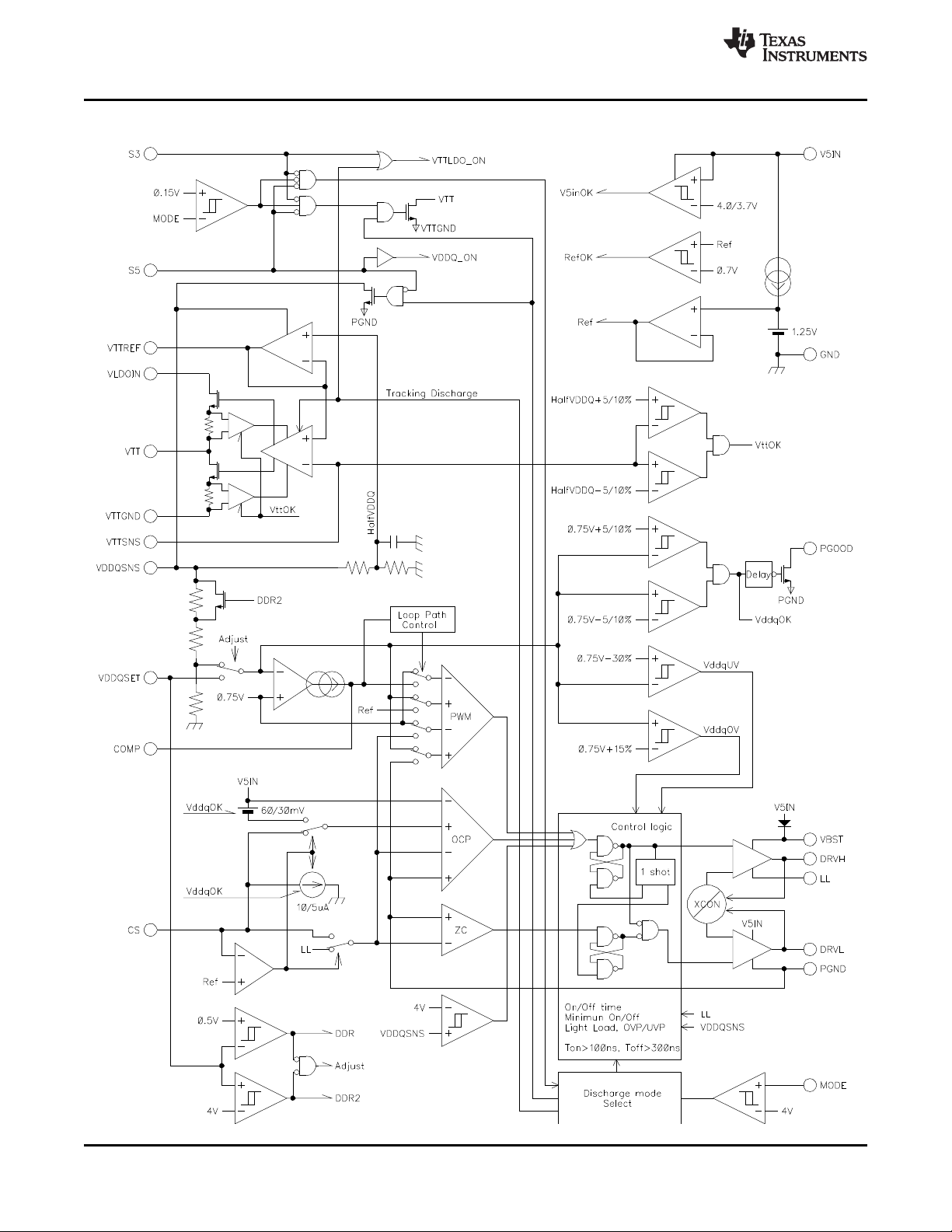
FUNCTIONAL BLOCK DIAGRAM (PWP)
10 Submit Documentation Feedback Copyright © 2004–2014, Texas Instruments Incorporated
Product Folder Links: TPS51116
Page 11
TI Information — Selective Disclosure
TPS51116
www.ti.com
SLUS609I –MAY 2004–REVISED JANUARY 2014
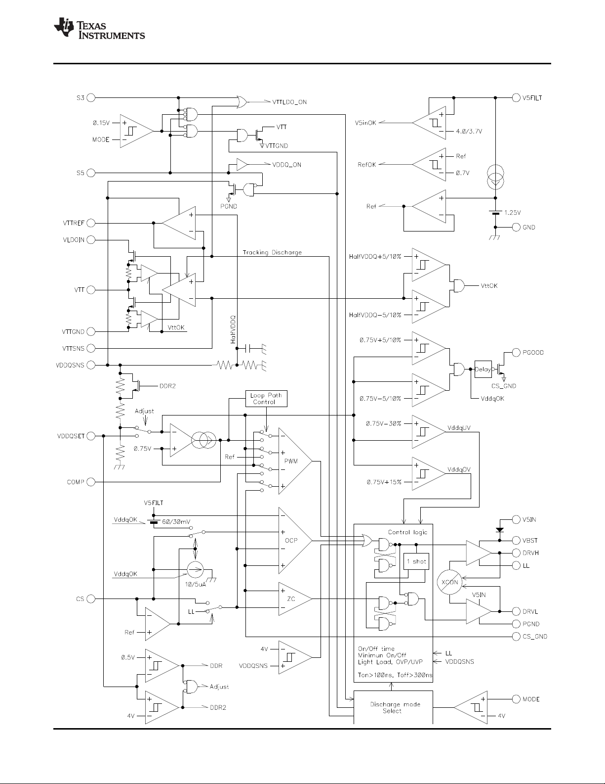
FUNCTIONAL BLOCK DIAGRAM (RGE)
Copyright © 2004–2014, Texas Instruments Incorporated Submit Documentation Feedback 11
Product Folder Links: TPS51116
Page 12

TPS51116
TI Information — Selective Disclosure
SLUS609I –MAY 2004–REVISED JANUARY 2014
www.ti.com
DETAILED DESCRIPTION
The TPS51116 is an integrated power management solution which combines a synchronous buck controller, a
10-mA buffered reference and a high-current sink/source low-dropout linear regulator (LDO) in a small 20-pin
HTSSOP package or a 24-pin QFN package. Each of these rails generates VDDQ, VTTREF and VTT that
required with DDR/DDR2/DDR3/LPDDR3 memory systems. The switch mode power supply (SMPS) portion
employs external N-channel MOSFETs to support high current for DDR/DDR2/DDR3/LPDDR3 memory
VDD/VDDQ. The preset output voltage is selectable from 2.5 V or 1.8 V. User-defined output voltage is also
possible and can be adjustable from 0.75 V to 3 V. Input voltage range of the SMPS is 3 V to 28 V. The SMPS
runs an adaptive on-time PWM operation at high-load condition and automatically reduces frequency to keep
excellent efficiency down to several mA. Current sensing scheme uses either R
MOSFET for a low-cost, loss-less solution, or an optional sense resistor placed in series to the rectifying
MOSFET for more accurate current limit. The output of the switcher is sensed by VDDQSNS pin to generate
one-half VDDQ for the 10-mA buffered reference (VTTREF) and the VTT active termination supply. The VTT
LDO can source and sink up to 3-A peak current with only 20-μF (two 10-μF in parallel) ceramic output
capacitors. VTTREF tracks VDDQ/2 within ±1% of VDDQ. VTT output tracks VTTREF within ±20 mV at no load
condition while ±40 mV at full load. The LDO input can be separated from VDDQ and optionally connected to a
lower voltage by using VLDOIN pin. This helps reducing power dissipation in sourcing phase. TheTPS51116 is
fully compatible to JEDEC DDR/DDR2 specifications at S3/S5 sleep state (see Table 2). The part has two
options of output discharge function when both VTT and VDDQ are disabled. The tracking discharge mode
discharges VDDQ and VTT outputs through the internal LDO transistors and then VTT output tracks half of
VDDQ voltage during discharge. The non-tracking discharge mode discharges outputs using internal discharge
MOSFETs which are connected to VDDQSNS and VTT. The current capability of these discharge FETs are
limited and discharge occurs more slowly than the tracking discharge. These discharge functions can be disabled
by selecting non-discharge mode.
of the external rectifying
DS(on)
VDDQ SMPS, Dual PWM Operation Modes
The main control loop of the SMPS is designed as an adaptive on-time pulse width modulation (PWM) controller.
It supports two control schemes which are a current mode and a proprietary D-CAP™ mode. D-CAP™ mode
uses internal compensation circuit and is suitable for low external component count configuration with an
appropriate amount of ESR at the output capacitor(s). Current mode control has more flexibility, using external
compensation network, and can be used to achieve stable operation with very low ESR capacitor(s) such as
ceramic or specialty polymer capacitors.
These control modes are selected by the COMP terminal connection. If the COMP pin is connected to V5IN,
TPS51116 works in the D-CAP™ mode, otherwise it works in the current mode. VDDQ output voltage is
monitored at a feedback point voltage. If VDDQSET is connected to V5IN or GND, this feedback point is the
output of the internal resistor divider inside VDDQSNS pin. If an external resistor divider is connected to
VDDQSET pin, VDDQSET pin itself becomes the feedback point (see VDDQ Output Voltage Selection section).
At the beginning of each cycle, the synchronous high-side MOSFET is turned on, or becomes ON state. This
MOSFET is turned off, or becomes OFF state, after internal one shot timer expires. This one shot is determined
by VINand V
control (see PWM Frequency and Adaptive On-Time Control section). The MOSFET is turned on again when
feedback information indicates insufficient output voltage and inductor current information indicates below the
overcurrent limit. Repeating operation in this manner, the controller regulates the output voltage. The
synchronous bottom or the rectifying MOSFET is turned on each OFF state to keep the conduction loss
minimum. The rectifying MOSFET is turned off when inductor current information detects zero level. This enables
seamless transition to the reduced frequency operation at light load condition so that high efficiency is kept over
broad range of load current.
In the current mode control scheme, the transconductance amplifier generates a target current level
corresponding to the voltage difference between the feedback point and the internal 750 mV reference. During
the OFF state, the PWM comparator monitors the inductor current signal as well as this target current level, and
when the inductor current signal comes lower than the target current level, the comparator provides SET signal
to initiate the next ON state. The voltage feedback gain is adjustable outside the controller device to support
various types of output MOSFETs and capacitors. In the D-CAP™ mode, the transconductance amplifier is
disabled and the PWM comparator compares the feedback point voltage and the internal 750 mV reference
during the OFF state. When the feedback point comes lower than the reference voltage, the comparator provides
SET signal to initiate the next ON state.
to keep frequency fairly constant over input voltage range, hence it is called adaptive on-time
OUT
12 Submit Documentation Feedback Copyright © 2004–2014, Texas Instruments Incorporated
Product Folder Links: TPS51116
Page 13

I
OUT(LL)
+
1
2 L f
(VIN* V
OUT
) V
OUT
V
IN
TI Information — Selective Disclosure
TPS51116
www.ti.com
SLUS609I –MAY 2004–REVISED JANUARY 2014
VDDQ SMPS, Light Load Condition
TPS51116 automatically reduces switching frequency at light load condition to maintain high efficiency. This
reduction of frequency is achieved smoothly and without increase of V
ripple or load regulation. Detail
OUT
operation is described as follows. As the output current decreases from heavy load condition, the inductor current
is also reduced and eventually comes to the point that its valley touches zero current, which is the boundary
between continuous conduction and discontinuous conduction modes. The rectifying MOSFET is turned off when
this zero inductor current is detected. As the load current further decreased, the converter runs in discontinuous
conduction mode and it takes longer and longer to discharge the output capacitor to the level that requires next
ON cycle. The ON-time is kept the same as that in the heavy load condition. In reverse, when the output current
increase from light load to heavy load, switching frequency increases to the constant 400 kHz as the inductor
current reaches to the continuous conduction. The transition load point to the light load operation I
OUT(LL)
(i.e. the
threshold between continuous and discontinuous conduction mode) can be calculated in Equation 1:
where
• f is the PWM switching frequency (400 kHz) (1)
Switching frequency versus output current in the light load condition is a function of L, f, VINand V
decreases almost proportional to the output current from the I
I
/10 and 4 kHz at I
OUT(LL)
OUT(LL)
/100.
OUT(LL)
given above. For example, it is 40 kHz at
OUT
, but it
Low-Side Driver
The low-side driver is designed to drive high-current, low-R
represented by the internal resistance, which is 3 Ω for V5IN to DRVL and 0.9 Ω for DRVL to PGND. A deadtime to prevent shoot through is internally generated between high-side MOSFET off to low-side MOSFET on,
and low-side MOSFET off to high-side MOSFET on. 5-V bias voltage is delivered from V5IN supply. The
instantaneous drive current is supplied by an input capacitor connected between V5IN and GND. The average
drive current is equal to the gate charge at VGS= 5 V times switching frequency. This gate drive current as well
as the high-side gate drive current times 5 V makes the driving power which needs to be dissipated from
TPS51116 package.
, N-channel MOSFET(s). The drive capability is
DS(on)
High-Side Driver
The high-side driver is designed to drive high-current, low on-resistance, N-channel MOSFET(s). When
configured as a floating driver, 5-V bias voltage is delivered from V5IN supply. The average drive current is also
calculated by the gate charge at VGS= 5V times switching frequency. The instantaneous drive current is supplied
by the flying capacitor between VBST and LL pins. The drive capability is represented by the internal resistance,
which is 3 Ω for VBST to DRVH and 0.9 Ω for DRVH to LL.
Current Sensing Scheme
In order to provide both good accuracy and cost effective solution, TPS51116 supports both of external resistor
sensing and MOSFET R
should be connected between the source terminal of the low-side MOSFET and PGND. CS pin is connected to
the MOSFET source terminal node. The inductor current is monitored by the voltage between PGND pin and CS
pin. For R
sensing scheme, CS pin should be connected to V5IN (PWP), or V5FILT (RGE) through the trip
DS(on)
voltage setting resistor, R
voltage across the R
. The inductor current is monitored by the voltage between PGND pin and LL pin so that
TRIP
LL pin should be connected to the drain terminal of the low-side MOSFET. I
slope to compensate the temperature dependency of the R
current sensing node so that PGND should be connected to the proper current sensing device, i.e. the sense
resistor or the source terminal of the low-side MOSFET.
sensing. For resistor sensing scheme, an appropriate current sensing resistor
DS(on)
. In this scheme, CS terminal sinks 10-μA I
TRIP
DS(on)
. In either scheme, PGND is used as the positive
current and the trip level is set to the
TRIP
has 4500ppm/°C temperature
TRIP
Copyright © 2004–2014, Texas Instruments Incorporated Submit Documentation Feedback 13
Product Folder Links: TPS51116
Page 14
TPS51116
TI Information — Selective Disclosure
SLUS609I –MAY 2004–REVISED JANUARY 2014
www.ti.com
PWM Frequency and Adaptive On-Time Control
TPS51116 includes an adaptive on-time control scheme and does not have a dedicated oscillator on board.
However, the device runs with fixed 400-kHz pseudo-constant frequency by feed-forwarding the input and output
voltage into the on-time one-shot timer. The on-time is controlled inverse proportional to the input voltage and
proportional to the output voltage so that the duty ratio is kept as V
OUT/VIN
technically with the same cycle time.
Although the TPS51116 does not have a pin connected to VIN, the input voltage is monitored at LL pin during
the ON state. This helps pin count reduction to make the part compact without sacrificing its performance. In
order to secure minimum ON-time during startup, feed-forward from the output voltage is enabled after the output
becomes 750 mV or larger.
VDDQ Output Voltage Selection
TPS51116 can be used for both of DDR (V
output voltage (0.75 V < V
output voltage scheme for a DDR3 (V
< 3 V) by connecting VDDQSET pin as shown in Table 1. Use the adjustable
VDDQ
VDDQ
Table 1. VDDQSET and Output Voltages
VDDQSET VDDQ (V) VTTREF and VTT NOTE
GND 2.5 V
V5IN 1.8 V
FB Resistors Adjustable V
= 2.5 V) and DDR2 (V
VDDQ
= 1.5 V) or LPDDR3 (V
= 1.8 V) power supply and adjustable
VDDQ
= 1.2 V) application.
VDDQ
/2 DDR
VDDQSNS
/2 DDR2
VDDQSNS
/2 0.75 V < V
VDDQSNS
VDDQ
< 3 V
(1)(2)
VTT Linear Regulator and VTTREF
TPS51116 integrates high performance low-dropout linear regulator that is capable of sourcing and sinking
current up to 3 A. This VTT linear regulator employs ultimate fast response feedback loop so that small ceramic
capacitors are enough to keep tracking the VTTREF within ±40 mV at all conditions including fast load transient.
To achieve tight regulation with minimum effect of wiring resistance, a remote sensing terminal, VTTSNS, should
be connected to the positive node of VTT output capacitor(s) as a separate trace from VTT pin. For stable
operation, total capacitance of the VTT output terminal can be equal to or greater than 20 μF. It is recommended
to attach two 10-μF ceramic capacitors in parallel to minimize the effect of ESR and ESL. If ESR of the output
capacitor is greater than 2 mΩ, insert an RC filter between the output and the VTTSNS input to achieve loop
stability. The RC filter time constant should be almost the same or slightly lower than the time constant made by
the output capacitor and its ESR. VTTREF block consists of on-chip 1/2 divider, LPF and buffer. This regulator
also has sink and source capability up to 10 mA. Bypass VTTREF to GND by a 0.033-μF ceramic capacitor for
stable operation.
When VTT is not required in the design, following treatment is strongly recommended.
• Connect VLDOIN to VDDQSNS.
• Tie VTTSNS to VTT, and remove capacitors from VTT to float.
• Connect VTTGND and MODE to GND (Non-tracking discharge mode as shown in Table 3)
• Maintain a 0.033-µF capacitor connected at VTTREF.
• Pull down S3 to GND with 1 kΩ of resistance.
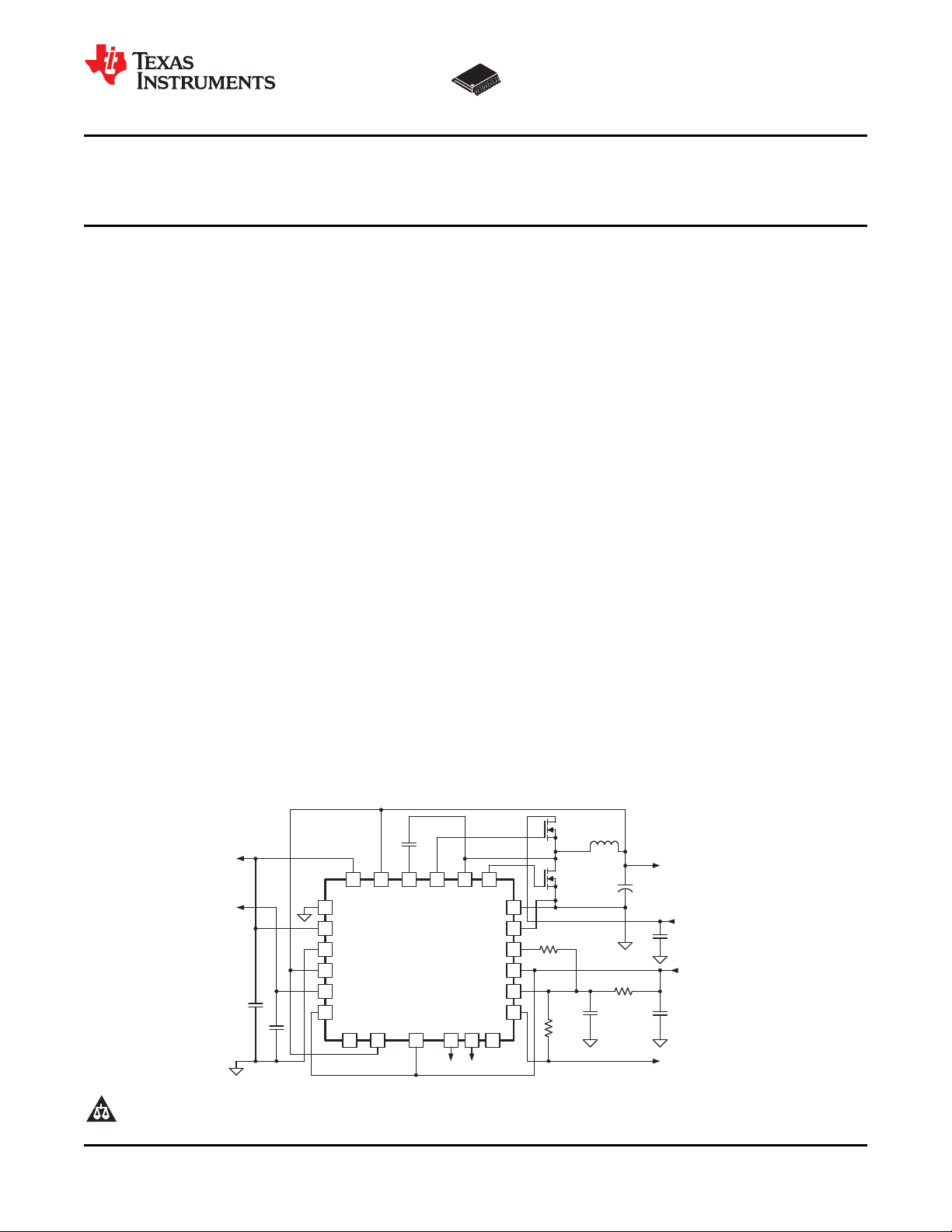
A typical circuit for this application is shown in Figure 1
(1) V
(2) Including DDR3 and LPDDR3
14 Submit Documentation Feedback Copyright © 2004–2014, Texas Instruments Incorporated
≥ 1.2 V when used as VLDOIN.
VDDQ
Product Folder Links: TPS51116
Page 15

PGOOD
S5
TPS51116 PWP
VLDOIN
VTT
UDG-12044
VTTGND
GND
MODE
1
2
3
5
6
5VIN
VDDQ
VIN
0.033 ?F
VTTREF
COMP
VDDQSNS
8
9
7
20
19
PGND
DRVH
LL
18
17
16
DRVL
VBST
15
14
S3
V5IN
PGOOD
13
12
11
S5
CS
4 VTTSNS
1 kW
VDDQSET10
TI Information — Selective Disclosure
TPS51116
www.ti.com
SLUS609I –MAY 2004–REVISED JANUARY 2014
Figure 1. Application Circuit When VTT Is Not Required
Controling Outputs Using the S3 and S5 Pins
In the DDR/DDR2/DDR3/LPDDR3 memory applications, it is important to keep VDDQ always higher than
VTT/VTTREF including both start-up and shutdown. TPS51116 provides this management by simply connecting
both the S3 and S5 pins to the sleep-mode signals such as SLP_S3 and SLP_S5 in the notebook PC system. All
of VDDQ, VTTREF and VTT are turned on at S0 state (S3 = S5 = high). In S3 state (S3 = low, S5 = high), VDDQ
and VTTREF voltages are kept on while VTT is turned off and left at high impedance (high-Z) state. The VTT
output is floated and does not sink or source current in this state. In S4/S5 states (S3 = S5 = low), all of the three
outputs are disabled. Outputs are discharged to ground according to the discharge mode selected by MODE pin
(see VDDQ and VTT Discharge Control section). Each state code represents as follow; S0 = full ON, S3 =
suspend to RAM (STR), S4 = suspend to disk (STD), S5 = soft OFF. (See Table 2)
Table 2. Sleep Mode Control Using the S3 and S5 Pins
STATE S3 S5 VDDQ VTTREF VTT
S0 HI HI ON ON ON
S3 LO HI ON ON OFF (High-Z)
S4/S5 LO LO OFF (Discharge) Off (Discharge) OFF (Discharge)
Soft-Start and Powergood
The soft start function of the SMPS is achieved by ramping up reference voltage and two-stage current clamp. At
the starting point, the reference voltage is set to 650 mV (87% of its target value) and the overcurrent threshold
is set half of the nominal value. When UVP comparator detects VDDQ become greater than 80% of the target,
the reference voltage is raised toward 750 mV using internal 4-bit DAC. This takes approximately 85 μs. The
overcurrent threshold is released to nominal value at the end of this period. The powergood signal waits another
45 μs after the reference voltage reaches 750 mV and the VDDQ voltage becomes good (above 95% of the
target voltage), then turns off powergood open-drain MOSFET.
The soft-start function of the VTT LDO is achieved by current clamp. The current limit threshold is also changed
in two stages using an internal powergood signal dedicated for LDO. During VTT is below the powergood
threshold, the current limit level is cut into 60% (2.2 A).This allows the output capacitors to be charged with low
and constant current that gives linear ramp up of the output. When the output comes up to the good state, the
overcurrent limit level is released to normal value (3.8 A). TPS51116 has an independent counter for each
output, but the PGOOD signal indicates only the status of VDDQ and does not indicate VTT powergood
externally. See Figure 2.
Copyright © 2004–2014, Texas Instruments Incorporated Submit Documentation Feedback 15
Product Folder Links: TPS51116
Page 16

VTT VTT
VTTSS
VTTOCL
C V
t
I
´
=
VDDQ VDDQ
VDDQSS
VDDQOCP
2 C V 0.8
t 85 s
I
´ ´ ´
= + m
V
OCL
V
VDDQ
V
PGOOD
V
S5
80%
87%
100%
85 µs
45 µs
UDG−04066
TPS51116
TI Information — Selective Disclosure
SLUS609I –MAY 2004–REVISED JANUARY 2014
Figure 2. VDDQ Soft-Start and Powergood Timing
www.ti.com
Soft-start duration, t
VDDQSS
, t
are functions of output capacitances.
VTTSS
where
• I
VDDQOCP
is the current limit value for VDDQ switcher calculated by Equation 5 (2)
where
• I
= 2.2 A (typ) (3)
VTTOCL
In both Equation 2 and Equation 3 , no load current during start-up are assumed. Note that both switchers and
the LDO do not start up with full load condition.
16 Submit Documentation Feedback Copyright © 2004–2014, Texas Instruments Incorporated
Product Folder Links: TPS51116
Page 17

I
OCP
+
V
TRIP
R
DS(on)
)
I
RIPPLE
2
+
V
TRIP
R
DS(on)
)
1
2 L f
ǒ
VIN* V
OUT
Ǔ
V
OUT
V
IN
V
TRIP
(mV) + R
TRIP
(kW) 10 (mA)
TI Information — Selective Disclosure
TPS51116
www.ti.com
SLUS609I –MAY 2004–REVISED JANUARY 2014
VDDQ and VTT Discharge Control
TPS51116 discharges VDDQ, VTTREF and VTT outputs when S3 and S5 are both low. There are two different
discharge modes. The discharge mode can be set by connecting MODE pin as shown in Table 3.
Table 3. Discharge Selection
MODE DISCHARGE MODE
V5IN No discharge
VDDQ Tracking discharge
GND Non-tracking discharge
When in tracking-discharge mode, TPS51116 discharges outputs through the internal VTT regulator transistors
and VTT output tracks half of VDDQ voltage during this discharge. Note that VDDQ discharge current flows via
VLDOIN to LDOGND thus VLDOIN must be connected to VDDQ output in this mode. The internal LDO can
handle up to 3 A and discharge quickly. After VDDQ is discharged down to 0.2 V, the internal LDO is turned off
and the operation mode is changed to the non-tracking-discharge mode.
When in non-tracking-discharge mode, TPS51116 discharges outputs using internal MOSFETs which are
connected to VDDQSNS and VTT. The current capability of these MOSFETs are limited to discharge slowly.
Note that VDDQ discharge current flows from VDDQSNS to PGND in this mode. In no discharge mode,
TPS51116 does not discharge any output charge.
Current Protection for VDDQ
The SMPS has cycle-by-cycle overcurrent limiting control. The inductor current is monitored during the OFF state
and the controller keeps the OFF state during the inductor current is larger than the overcurrent trip level. The
trip level and current sense scheme are determined by CS pin connection (see Current Sensing Scheme
section). For resistor sensing scheme, the trip level, V
For R
sensing scheme, CS terminal sinks 10 μA and the trip level is set to the voltage across this R
DS(on)
resistor.
, is fixed value of 60 mV.
TRIP
TRIP
(4)
As the comparison is done during the OFF state, V
current at overcurrent threshold, I
, can be calculated as shown in Equation 5.
OCP
sets valley level of the inductor current. Thus, the load
TRIP
(5)
In an overcurrent condition, the current to the load exceeds the current to the output capacitor thus the output
voltage tends to fall down. If the output voltage becomes less than Powergood level, the V
is cut into half and
TRIP
the output voltage tends to be even lower. Eventually, it crosses the undervoltage protection threshold and
shutdown.
Current Protection for VTT
The LDO has an internally fixed constant overcurrent limiting of 3.8 A while operating at normal condition. This
trip point is reduced to 2.2 A before the output voltage comes within ±5% of the target voltage or goes outside of
±10% of the target voltage.
Copyright © 2004–2014, Texas Instruments Incorporated Submit Documentation Feedback 17
Product Folder Links: TPS51116
Page 18

TPS51116
TI Information — Selective Disclosure
SLUS609I –MAY 2004–REVISED JANUARY 2014
www.ti.com
Overvoltage and Undervoltage Protection for VDDQ
TPS51116 monitors a resistor divided feedback voltage to detect overvoltage and undervoltage. If VDDQSET is
connected to V5IN or GND, the feedback voltage is made by an internal resistor divider inside VDDQSNS pin. If
an external resistor divider is connected to VDDQSET pin, the feedback voltage is VDDQSET voltage itself.
When the feedback voltage becomes higher than 115% of the target voltage, the OVP comparator output goes
high and the circuit latches as the high-side MOSFET driver OFF and the low-side MOSFET driver ON.
Also, TPS51116 monitors VDDQSNS voltage directly and if it becomes greater than 4 V TPS51116 turns off the
high-side MOSFET driver. When the feedback voltage becomes lower than 70% of the target voltage, the UVP
comparator output goes high and an internal UVP delay counter begins counting. After 32 cycles, TPS51116
latches OFF both top and low-side MOSFETs. This function is enabled after 1007 cycles of SMPS operation to
ensure startup.
V5IN (PWP), V5FILT (RGE) Undervoltage Lockout (UVLO) Protection
TPS51116 has 5-V supply undervoltage lockout protection (UVLO). When the V5IN (PWP) voltage or V5FILT
(RGE) voltage is lower than UVLO threshold voltage, SMPS, VTTLDO and VTTREF are shut off. This is a nonlatch protection.
V5IN (PWP), V5FILT (RGE) Input Capacitor
Add a ceramic capacitor with a value between 1.0 μF and 4.7 μF placed close to the V5IN (PWP) pin or V5FILT
(RGE) pin to stabilize 5 V from any parasitic impedance from the supply.
Thermal Shutdown
TPS51116 monitors the temperature of itself. If the temperature exceeds the threshold value, 160°C (typ),
SMPS, VTTLDO and VTTREF are shut off. This is a non-latch protection and the operation is resumed when the
device is cooled down by about 10°C.
18 Submit Documentation Feedback Copyright © 2004–2014, Texas Instruments Incorporated
Product Folder Links: TPS51116
Page 19

wP2+
1
ǒ
CO RL
Ǔ
wP1+
1
ǒ
CC R
O
Ǔ
H3(s) +
(1 ) s CO ESR)
ǒ
1 ) s CO RL
Ǔ
RL
R
S
H2(s) + * gm
R
O
ǒ
1 ) s CC R
C
Ǔ
ǒ
1 ) s CC R
O
Ǔ ǒ
1 ) s CC2 R
C
Ǔ
H1(s) +
R2
(
R2) R1
)
H(s) + H1(s) H2(s) H3(s)
TI Information — Selective Disclosure
TPS51116
www.ti.com
SLUS609I –MAY 2004–REVISED JANUARY 2014
APPLICATION INFORMATION
Loop Compensation and External Parts Selection
Current Mode Operation
A buck converter using TPS51116 current mode operation can be partitioned into three portions, a voltage
divider, an error amplifier and a switching modulator. By linearizing the switching modulator, we can derive the
transfer function of the whole system. Because current mode scheme directly controls the inductor current, the
modulator can be linearized as shown in Figure 3.
Figure 3. Linearizing the Modulator
Here, the inductor is located inside the local feedback loop and its inductance does not appear in the small signal
model. As a result, a modulated current source including the power inductor can be modeled as a current source
with its transconductance of 1/RSand the output capacitor represent the modulator portion. This simplified model
is applicable in the frequency space up to approximately a half of the switching frequency. One note is, although
the inductance has no influence to small signal model, it has influence to the large signal model as it limits slew
rate of the current source. This means the buck converter’s load transient response, one of the large signal
behaviors, can be improved by using smaller inductance without affecting the loop stability.
Total open loop transfer function of the whole system is given by Equation 6.
(6)
Assuming RL>>ESR, RO>>RCand CC>>CC2, each transfer function of the three blocks is shown starting with
Equation 7.
(7)
(8)
(9)
There are three poles and two zeros in H(s). Each pole and zero is given by the following five equations.
Copyright © 2004–2014, Texas Instruments Incorporated Submit Documentation Feedback 19
(10)
(11)
Product Folder Links: TPS51116
Page 20

O
C2
C
C ESR
C
R
´
=
wz2+
1
ǒ
CO ESR
Ǔ
+ wp3+
1
ǒ
CC2 R
C
Ǔ
RC+ 2.8 V
OUT
CO[mF] RS[mW]
RCv 2p f
0
V
OUT
0.75
C
O
gm
R
S
I
IND(peak)
+
V
TRIP
R
DS(on)
)
1
L f
ǒ
V
IN(max)
* V
OUT
Ǔ
V
OUT
V
IN(max)
L +
1
I
IND(ripple)
f
ǒ
V
IN(max)
* V
OUT
Ǔ
V
OUT
V
IN(max)
+
2
I
OUT(max)
f
ǒ
V
IN(max)
* V
OUT
Ǔ
V
OUT
V
IN(max)
f
0
+
1
2p
R1
R1) R2
gm
C
O
R
C
R
S
+
1
2p
0.75
V
OUT
gm
C
O
R
C
R
S
wZ2+
1
ǒ
CO ESR
Ǔ
wZ1+
1
ǒ
CC R
C
Ǔ
wP3+
1
ǒ
CC2 R
C
Ǔ
TPS51116
TI Information — Selective Disclosure
SLUS609I –MAY 2004–REVISED JANUARY 2014
www.ti.com
(12)
(13)
(14)
Usually, each frequency of those poles and zeros is lower than the 0 dB frequency, f0. However, the f0should be
kept under 1/3 of the switching frequency to avoid effect of switching circuit delay. The f0is given by Equation 15.
(15)
Based on small signal analysis above, the external components can be selected by following manner.
1. Choose the inductor. The inductance value should be determined to give the ripple current of
approximately 1/4 to 1/2 of maximum output current.
(16)
The inductor also needs to have low DCR to achieve good efficiency, as well as enough room above peak
inductor current before saturation. The peak inductor current can be estimated as shown in Equation 17.
(17)
2. Choose rectifying (bottom) MOSFET. When R
on-resistance is used as this RSso that lower R
sensing scheme is selected, the rectifying MOSFET’s
DS(on)
does not always promise better performance. In order
DS(on)
to clearly detect inductor current, minimum RSrecommended is to give 15 mV or larger ripple voltage with
the inductor ripple current. This promises smooth transition from CCM to DCM or vice versa. Upper side of
the R
is of course restricted by the efficiency requirement, and usually this resistance affects efficiency
DS(on)
more at high-load conditions. When using external resistor current sensing, there is no restriction for low
R
. However, the current sensing resistance RSitself affects the efficiency
DS(on)
3. Choose output capacitor(s). When organic semiconductor capacitors (OS-CON) or specialty polymer
capacitors (SP-CAP) are used, ESR to achieve required ripple value at stable state or transient load
conditions determines the amount of capacitor(s) need, and capacitance is then enough to satisfy stable
operation. The peak-to-peak ripple value can be estimated by ESR times the inductor ripple current for stable
state, or ESR times the load current step for a fast transient load response. When ceramic capacitor(s) are
used, the ESR is usually small enough to meet ripple requirement. In contrast, transient undershoot and
overshoot driven by output capacitance becomes the key factor in determining the capacitor(s) required.
4. Determine f0and calculate RCusing Equation 18. Note that higher RCshows faster transient response in
cost of unstableness. If the transient response is not enough even with high RCvalue, try increasing the out
put capacitance. Recommended f0is f
/4. Then RCcan be derived by Equation 19.
OSC
(18)
(19)
5. Calculate CC2. Purpose of this capacitance is to cancel zero caused by ESR of the output capacitor. When
ceramic capacitor(s) are used, no need for CC2.
20 Submit Documentation Feedback Copyright © 2004–2014, Texas Instruments Incorporated
Product Folder Links: TPS51116
(20)
(21)
Page 21

f
0
+
1
2p ESR C
O
v
f
SW
3
R1 +
V
OUT
* 0.75
0.75
R2
f
z1
+
1
2p CC R
C
+
f
0
10
TI Information — Selective Disclosure
TPS51116
www.ti.com
SLUS609I –MAY 2004–REVISED JANUARY 2014
6. Calculate CC. The purpose of CCis to cut DC component to obtain high DC feedback gain. However, as it
causes phase delay, another zero to cancel this effect at f0frequency is need. This zero, ωz1, is determined
by Cc and Rc. Recommended ωz1 is 10 times lower to the f0frequency.
(22)
7. When using adjustable mode, determine the value of R1 and R2. .
(23)
D-CAP™ Mode Operation
A buck converter system using D-CAP™ Mode can be simplified as below.
Figure 4. Linearizing the Modulator
The PWM comparator compares the VDDQSNS voltage divided by R1 and R2 with internal reference voltage,
and determines the timing to turn on the high-side MOSFET. The gain and speed of the comparator is high
enough to keep the voltage at the beginning of each on cycle (or the end of off cycle) substantially constant. The
DC output voltage may have line regulation due to ripple amplitude that slightly increases as the input voltage
increase.
For the loop stability, the 0-dB frequency, f0, defined below need to be lower than 1/3 of the switching frequency.
(24)
As f0is determined solely by the output capacitor’s characteristics, loop stability of D-CAP™ mode is determined
by the capacitor’s chemistry. For example, specialty polymer capacitors (SP-CAP) have COin the order of
several 100 μF and ESR in range of 10 mΩ. These makes f0in the order of 100 kHz or less and the loop is then
stable. However, ceramic capacitors have f0at more than 700 kHz, which is not suitable for this operational
mode.
Although D-CAP™ mode provides many advantages such as ease-of-use, minimum external components
configuration and extremely short response time, due to not employing an error amplifier in the loop, sufficient
amount of feedback signal needs to be provided by external circuit to reduce jitter level.
The required signal level is approximately 15 mV at comparing point. This gives V
RIPPLE
= (V
/0.75) x 15 (mV)
OUT
at the output node. The output capacitor’s ESR should meet this requirement.
The external components selection is much simple in D-CAP™ mode.
1. Choose inductor. This section is the same as the current mode. Please refer to the instructions in the
Current Mode Operation section.
2. Choose output capacitor(s).Organic semiconductor capacitor(s) or specialty polymer capacitor(s) are
recommended. Determine ESR to meet required ripple voltage above. A quick approximation is shown in
Copyright © 2004–2014, Texas Instruments Incorporated Submit Documentation Feedback 21
Product Folder Links: TPS51116
Page 22

W
PKG
+
T
J(max)
* T
A(max)
q
JA
W
DSNK
+ V
VTT
I
VTT
W
DSRC
+
ǒ
V
VLDOIN
* V
VTT
Ǔ
I
VTT
ESR +
V
OUT
0.015
I
RIPPLE
0.75
[
VOUT
I
OUT(max)
60 [mW]
TPS51116
TI Information — Selective Disclosure
SLUS609I –MAY 2004–REVISED JANUARY 2014
www.ti.com
Equation 25.
(25)
Thermal Design
Primary power dissipation of TPS51116 is generated from VTT regulator. VTT current flow in both source and
sink directions generate power dissipation from the part. In the source phase, potential difference between
VLDOIN and VTT times VTT current becomes the power dissipation, W
In this case, if VLDOIN is connected to an alternative power supply lower than VDDQ voltage, power loss can be
decreased.
For the sink phase, VTT voltage is applied across the internal LDO regulator, and the power dissipation, W
is calculated by Equation 27:
Because this device does not sink AND source the current at the same time and I
actual power dissipation need to be considered for thermal design is an average of above value. Another power
consumption is the current used for internal control circuitry from V5IN supply and VLDOIN supply. V5IN
supports both the internal circuit and external MOSFETs drive current. The former current is in the VLDOIN
supply can be estimated as 1.5 mA or less at normal operational conditions.
These powers need to be effectively dissipated from the package. Maximum power dissipation allowed to the
package is calculated by Equation 28,
DSRC
.
(26)
DSNK
(27)
varies rapidly with time,
VTT
,
(28)
where
• T
• T
is 125°C
J(max)
is the maximum ambient temperature in the system
A(max)
• θJAis the thermal resistance from the silicon junction to the ambient
This thermal resistance strongly depends on the board layout. TPS51116 is assembled in a thermally enhanced
PowerPAD™ package that has exposed die pad underneath the body. For improved thermal performance, this
die pad needs to be attached to ground trace via thermal land on the PCB. This ground trace acts as a heat
sink/spread. The typical thermal resistance, 39.6°C/W, is achieved based on a 6.5 mm × 3.4 mm thermal land
with eight vias without air flow. It can be improved by using larger thermal land and/or increasing vias number.
Further information about PowerPAD™ and its recommended board layout is described in (SLMA002). This
document is available at http:\\www.ti.com.
22 Submit Documentation Feedback Copyright © 2004–2014, Texas Instruments Incorporated
Product Folder Links: TPS51116
Page 23

TI Information — Selective Disclosure
TPS51116
www.ti.com
SLUS609I –MAY 2004–REVISED JANUARY 2014
Layout Considerations
Certain points must be considered before designing a layout using the TPS51116.
• PCB trace defined as LL node, which connects to source of switching MOSFET, drain of rectifying MOSFET
and high-voltage side of the inductor, should be as short and wide as possible.
• Consider adding a small snubber circuit, consisting of a 3-Ω resitor and a 1-nF capacitor, between LL and
PGND in case a high-frequency surge is observed on the LL voltage waveform.
• All sensitive analog traces such as VDDQSNS, VTTSNS and CS should placed away from high-voltage
switching nodes such as LL, DRVL or DRVH nodes to avoid coupling.
• VLDOIN should be connected to VDDQ output with short and wide trace. If different power source is used for
VLDOIN, an input bypass capacitor should be placed to the pin as close as possible with short and wide
connection.
• The output capacitor for VTT should be placed close to the pin with short and wide connection in order to
avoid additional ESR and/or ESL of the trace.
• VTTSNS should be connected to the positive node of VTT output capacitor(s) as a separate trace from the
high current power line and is strongly recommended to avoid additional ESR and/or ESL. If it is needed to
sense the voltage of the point of the load, it is recommended to attach the output capacitor(s) at that point.
Also, it is recommended to minimize any additional ESR and/or ESL of ground trace between GND pin and
the output capacitor(s).
• Consider adding LPF at VTTSNS when the ESR of the VTT output capacitor(s) is larger than 2 mΩ.
• VDDQSNS can be connected separately from VLDOIN. Remember that this sensing potential is the reference
voltage of VTTREF. Avoid any noise generative lines.
• Negative node of VTT output capacitor(s) and VTTREF capacitor should be tied together by avoiding
common impedance to the high current path of the VTT source/sink current.
• GND (Signal GND) pin node represents the reference potential for VTTREF and VTT outputs. Connect GND
to negative nodes of VTT capacitor(s), VTTREF capacitor and VDDQ capacitor(s) with care to avoid
additional ESR and/or ESL. GND and PGND (power ground) should be connected together at a single point.
• Connect CS_GND (RGE) to source of rectifying MOSFET using Kevin connection. Avoid common trace for
high-current paths such as the MOSFET to the output capacitors or the PGND to the MOSFET trace. When
using an external current sense resistor, apply the same care and connect it to the positive side (ground side)
of the resistor.
• PGND is the return path for rectifying MOSFET gate drive. Use 0.65 mm (25mil) or wider trace. Connect to
source of rectifying MOSFET with shortest possible path.
• Place a V5FILT filter capacitor (RGE) close to the TPS51116, within 12 mm (0.5 inches) if possible.
• The trace from the CS pin should avoid high-voltage switching nodes such as those for LL, VBST, DRVH,
DRVL or PGOOD.
• In order to effectively remove heat from the package, prepare thermal land and solder to the package’s
thermal pad. Wide trace of the component-side copper, connected to this thermal land, helps heat spreading.
Numerous vias with a 0.33-mm diameter connected from the thermal land to the internal/solder-side ground
plane(s) should be used to help dissipation. Do NOT connect PGND to this thermal land underneath the
package.
Copyright © 2004–2014, Texas Instruments Incorporated Submit Documentation Feedback 23
Product Folder Links: TPS51116
Page 24

TPS51116
TI Information — Selective Disclosure
SLUS609I –MAY 2004–REVISED JANUARY 2014
www.ti.com
Figure 5. D-CAP™ Mode, PWP Package
Figure 6. D-CAP™ Mode, RGE Package
Table 4. D-CAP™ Mode Schematic Components
SYMBOL SPECIFICATION MANUFACTURER PART NUMBER
R1 5.1 kΩ R2 100 kΩ R3 75 kΩ R4 (100 × V
R5 5.1 Ω
M1 30 V, 13 mΩ International Rectifier IRF7821
M2 30 V, 5 mΩ International Rectifier IRF7832
24 Submit Documentation Feedback Copyright © 2004–2014, Texas Instruments Incorporated
– 75) kΩ -
VDDQ
Product Folder Links: TPS51116
Page 25

TI Information — Selective Disclosure
TPS51116
www.ti.com
SLUS609I –MAY 2004–REVISED JANUARY 2014
Figure 7. Current Mode, PWP Package
Figure 8. Current Mode, RGE Package
Table 5. Current Mode Schematic Components
SYMBOL SPECIFICATION MANUFACTURER PART NUMBER
R1 6 mΩ, 1% Vishay WSL-2521 0.006
R2 100 kΩ - R5 5.1 Ω
M0 30 V, 13 mΩ International Rectifier IRF7821
M1 30 V, 5 mΩ International Rectifier IRF7832
Copyright © 2004–2014, Texas Instruments Incorporated Submit Documentation Feedback 25
Product Folder Links: TPS51116
Page 26

T
J
− Junction Temperature − °C
I
VLDOIN
− VLDOIN Supply Current − µA
0
−50 0 50 100 150
1.0
0.9
0.8
0.7
0.6
0.5
0.4
0.3
0.2
0.1
I
VTT
− VTT Current − A
I
V5IN
− V5IN Supply Current − mA
−2
3
0
−1
0 1 2
1
2
7
4
5
6
10
8
9
DDR2
V
VTT
= 0.9 V
−50
2.0
0
0
1.8
1.6
1.4
1.2
1.0
0.8
0.6
0.4
0.2
50 100 150
T
J
− Junction Temperature − °C
I
V5IN1
− V5IN Supply Current − mA
T
J
− Junction Temperature − °C
I
V5IN1
− V5IN Shutdown Current − µA
0
−50 0 50 100 150
1.0
0.9
0.8
0.7
0.6
0.5
0.4
0.3
0.2
0.1
TPS51116
TI Information — Selective Disclosure
SLUS609I –MAY 2004–REVISED JANUARY 2014
TYPICAL CHARACTERISTICS
All data in the following graphs are measured from the PWP packaged device.
V5IN SUPPLY CURRENT V5IN SHUTDOWN CURRENT
JUNCTION TEMPERATURE JUNCTION TEMPERATURE
vs vs
www.ti.com
Figure 9. Figure 10.
V5IN SUPPLY CURRENT VLDOIN SUPPLY CURRENT
vs vs
LOAD CURRENT TEMPERATURE
Figure 11. Figure 12.
26 Submit Documentation Feedback Copyright © 2004–2014, Texas Instruments Incorporated
Product Folder Links: TPS51116
Page 27

T
J
− Junction Temperature − °C
I
DISCH
− VTT Discharge Current − mA
15
10
25
20
30
−50 0 50 100 150
T
J
− Junction Temperature − °C
V
TRIP
− OVP/UVP Trip Threshold − %
60
−50 0 50 100 150
80
120
100
140
V
UVP
V
OVP
T
J
− Junction Temperature − °C
I
TRIP
− CS Current − µA
2
0
−50 0 50 100 150
6
8
4
10
14
16
12
PGOOD = HI
PGOOD = LO
T
J
− Junction Temperature − °C
I
DISCH
− VDDQ Discharge Current − mA
30
40
50
70
80
60
20
10
−50 0 50 100 150
TI Information — Selective Disclosure
TPS51116
www.ti.com
SLUS609I –MAY 2004–REVISED JANUARY 2014
TYPICAL CHARACTERISTICS (continued)
CS CURRENT VDDQ DISCHARGE CURRENT
JUNCTION TEMPERATURE JUNCTION TEMPERATURE
vs vs
Figure 13. Figure 14.
VTT DISCHARGE CURRENT OVERVOLTAGE AND UNDERVOLTAGE THRESHOLD
JUNCTION TEMPERATURE JUNCTION TEMPERATURE
vs vs
Figure 15. Figure 16.
Copyright © 2004–2014, Texas Instruments Incorporated Submit Documentation Feedback 27
Product Folder Links: TPS51116
Page 28

4 8 12 16 20 24 30
1.785
1.795
1.800
1.790
1.815
1.820
1.810
1.805
1.780
V
IN
− Input Voltage − V
V
VDDQ
− VDDQ Output Voltage − V
D−CAP Mode
I
VDDQ
= 0 A
I
VDDQ
= 10 A
0 2
1.785
1.795
1.800
1.790
1.815
1.820
1.810
1.805
1.780
4 6 8 10
I
VDDQ
− VDDQ Output Current − A
V
VDDQ
− VDDQ Output Voltage − V
D−CAP Mode
VIN = 12 V
V
IN
− Input Voltage − V
f
SW
− Switching Frequency − kHz
DDR2
4
390
370
8
12 16 20 24 28
380
420
400
410
430
D-CAP Mode
I
VDDQ
= 7 A
DDR
0
0
2 4 6 8 10
100
150
50
300
400
450
350
250
200
I
VDDQ
− VDDQ Output Current − A
f
SW
− Switching Frequency − kHz
DDR2
D−CAP Mode
VIN = 12 V
DDR
TPS51116
TI Information — Selective Disclosure
SLUS609I –MAY 2004–REVISED JANUARY 2014
TYPICAL CHARACTERISTICS (continued)
SWITCHING FREQUENCY SWITCHING FREQUENCY
vs vs
INPUT VOLTAGE OUTPUT CURRENT
Figure 17. Figure 18.
www.ti.com
VDDQ OUTPUT VOLTAGE VDDQ OUTPUT VOLTAGE
OUTPUT CURRENT (DDR) INPUT VOLTAGE (DDR2)
Figure 19. Figure 20.
28 Submit Documentation Feedback Copyright © 2004–2014, Texas Instruments Incorporated
vs vs
Product Folder Links: TPS51116
Page 29

I
VTTREF
− VTTREF Current − mA
V
VTTREF
− VTTREF Voltage − V
−10 −5 0 5 10
0.897
0.896
0.898
0.899
0.900
0.901
0.902
0.903
0.904
DDR2
−10
1.245
1.244
−5
0 5 10
1.246
1.247
1.248
1.249
1.250
1.251
1.252
I
VTTREF
− VTTREF Current − mA
V
VTTREF
− VTTREF Voltage − V
DDR
I
VTT
− VTT Output Current − A
V
VTT
− VTT Output Voltage − V
−5
1.22
1.20
−4
−3 −2 −1 0 1 2 3 4 5
1.21
1.25
1.23
1.24
1.28
1.26
1.27
1.29
1.30
V
VLDOIN
= 2.5 V
V
VLDOIN
= 1.8 V
I
VTT
− VTT Output Current − A
V
VTT
− VTT Output Voltage − V
−3
0.88
0.86
−2
−1 0 1 2 3
0.87
0.91
0.89
0.90
0.94
0.92
0.93
V
VLDOIN
= 1.5 V
V
VLDOIN
= 1.2 V
V
VLDOIN
= 1.8 V
TI Information — Selective Disclosure
TPS51116
www.ti.com
SLUS609I –MAY 2004–REVISED JANUARY 2014
TYPICAL CHARACTERISTICS (continued)
VTT OUTPUT VOLTAGE VTT OUTPUT VOLTAGE
OUTPUT CURRENT (DDR) OUTPUT CURRENT (DDR2)
vs vs
Figure 21. Figure 22.
VTTREF OUTPUT VOLTAGE VTTREF OUTPUT VOLTAGE
OUTPUT CURRENT (DDR) OUTPUT CURRENT (DDR2)
vs vs
Figure 23. Figure 24.
Copyright © 2004–2014, Texas Instruments Incorporated Submit Documentation Feedback 29
Product Folder Links: TPS51116
Page 30

0.001
60
50
0.01
0.1 1 10
80
70
100
90
I
VDDQ
− VDDQ Current − A
Efficiency − %
V
VDDQ
= 2.5 V
V
IN
= 8 V
V
IN
= 20 V
V
IN
= 12 V
0.001
60
50
0.01 0.1 1 10
80
70
100
90
V
VDDQ
= 1.8 V
V
IN
= 8 V
V
IN
= 20 V
V
IN
= 12 V
I
VDDQ
− VDDQ Current − A
Efficiency − %
-3
0.73
0.71
-2
0.74
0.72
0.77
0.75
0.78
0.76
0.79
V
VLDOIN
= 1.5 V
-1
0
I
VTT
- VTT Output Current - A
1 2
3
I
VTT
- VTT Output Voltage - V
-10
0.735
-5
0
5
10
I
VTTREF
- VTTREF Current - mA
0.74
0.745
0.75
0.755
0.76
0.765
I
VTT
- VTT Output Voltage - V
DDR3
TPS51116
TI Information — Selective Disclosure
SLUS609I –MAY 2004–REVISED JANUARY 2014
TYPICAL CHARACTERISTICS (continued)
VTTREF OUTPUT VOLTAGE VTT OUTPUT VOLTAGE
OUTPUT CURRENT (DDR3) OUTPUT CURRENT (DDR3)
vs vs
www.ti.com
Figure 25. Figure 26.
VDDQ EFFICIENCY (DDR) VDDQ EFFICIENCY (DDR2)
vs vs
VDDQ CURRENT VDDQ CURRENT
Figure 27. Figure 28.
30 Submit Documentation Feedback Copyright © 2004–2014, Texas Instruments Incorporated
Product Folder Links: TPS51116
Page 31

t − Time − 20 µs/div
V
VDDQ
(50 mV/div)
V
VTT
(20 mV/div)
V
VTTREF
(20 mV/div)
I
VTT
(2 A/div)
t − Time − 100 µs/div
VDDQ
VTTREF
PGOOD
S5
I
VDDQ
= I
VTTREF
= 0 A
t − Time − 20 µs/div
V
VDDQ
(50 mV/div)
I
VDDQ
(5 A/div)
I
IND
(5 A/div)
t − Time − 2 µs/div
V
VDDQ
(50 mV/div)
I
VDDQ
(2 A/div)
V
VTTREF
(10 mV/div)
V
VTT
(10 mV/div)
TI Information — Selective Disclosure
TPS51116
www.ti.com
SLUS609I –MAY 2004–REVISED JANUARY 2014
TYPICAL CHARACTERISTICS (continued)
Figure 29. Ripple Waveforms - Heavy Load Condition Figure 30. VDDQ Load Transient Response
Figure 31. VTT Load Transient Response Figure 32. VDDQ, VTT, and VTTREF Start-Up Waveforms
Copyright © 2004–2014, Texas Instruments Incorporated Submit Documentation Feedback 31
Product Folder Links: TPS51116
Page 32

Gain − dB
Phase − 5
10 k
−40
−80
100 k
1 M
10 M
−60
20
−20
0
80
40
60
−90
45
−45
0
180
90
135
−180
−135
Phase
Gain
f − Frequency − Hz
I
VTT
= −1 A
100
−40
−80
1 k 100 k 1 M
−60
20
−20
0
80
40
60
−90
45
−45
0
180
90
135
−180
−135
f − Frequency − Hz
Gain − dB
Phase − 5
Phase
Gain
I
VDDQ
= 7 A
10 k
t − Time − 200 µs/div
VDDQ
VTTREF
VTT
S5
I
VDDQ
= I
VTT
= I
VTTREF
= 0 A
t − Time − 1 ms/div
VDDQ
VTTREF
VTT
S5
I
VDDQ
= I
VTT
= I
VTTREF
= 0 A
TPS51116
TI Information — Selective Disclosure
SLUS609I –MAY 2004–REVISED JANUARY 2014
TYPICAL CHARACTERISTICS (continued)
Figure 33. Soft-Start Waveforms Tracking Discharge Figure 34. Soft-Stop Waveforms Non-Tracking Discharge
VDDQ BODE PLOT (CURRENT MODE) VTT BODE PLOT, SOURCE (DDR2)
GAIN AND PHASE GAIN AND PHASE
vs vs
FREQUENCY FREQUENCY
www.ti.com
Figure 35. Figure 36.
32 Submit Documentation Feedback Copyright © 2004–2014, Texas Instruments Incorporated
Product Folder Links: TPS51116
Page 33

10 k
−40
−80
100 k
1 M
10 M
−60
20
−20
0
80
40
60
−90
45
−45
0
180
90
135
−180
−135
f − Frequency − Hz
Gain − dB
Phase
Gain
I
VTT
= 1 A
Phase − °
TI Information — Selective Disclosure
TPS51116
www.ti.com
SLUS609I –MAY 2004–REVISED JANUARY 2014
TYPICAL CHARACTERISTICS (continued)
VTT BODE PLOT, SINK (DDR2)
GAIN AND PHASE
vs
FREQUENCY
Figure 37.
Product Folder Links: TPS51116
Copyright © 2004–2014, Texas Instruments Incorporated Submit Documentation Feedback 33
Page 34

TPS51116
TI Information — Selective Disclosure
SLUS609I –MAY 2004–REVISED JANUARY 2014
Changes from Revision H (JULY 2009) to Revision I Page
• Added clarity to Features section ......................................................................................................................................... 1
• Added references to "LPDDR3 " to the Title and Description sections ................................................................................ 1
• Added reference to "SSTL-15" in Applications section ......................................................................................................... 1
• Added references to "LPDDR3 " to the Detailed Description section ................................................................................. 12
• Added clarity to Figure 1 ..................................................................................................................................................... 14
www.ti.com
34 Submit Documentation Feedback Copyright © 2004–2014, Texas Instruments Incorporated
Product Folder Links: TPS51116
Page 35

PACKAGE OPTION ADDENDUM
www.ti.com
11-Apr-2013
PACKAGING INFORMATION
Orderable Device Status
TPS51116PWP ACTIVE HTSSOP PWP 20 70 Green (RoHS
TPS51116PWPG4 ACTIVE HTSSOP PWP 20 70 Green (RoHS
TPS51116PWPR ACTIVE HTSSOP PWP 20 2000 Green (RoHS
TPS51116PWPRG4 ACTIVE HTSSOP PWP 20 2000 Green (RoHS
TPS51116RGER ACTIVE VQFN RGE 24 3000 Green (RoHS
TPS51116RGERG4 ACTIVE VQFN RGE 24 3000 Green (RoHS
TPS51116RGET ACTIVE VQFN RGE 24 250 Green (RoHS
TPS51116RGETG4 ACTIVE VQFN RGE 24 250 Green (RoHS
(1)
The marketing status values are defined as follows:
ACTIVE: Product device recommended for new designs.
LIFEBUY: TI has announced that the device will be discontinued, and a lifetime-buy period is in effect.
NRND: Not recommended for new designs. Device is in production to support existing customers, but TI does not recommend using this part in a new design.
PREVIEW: Device has been announced but is not in production. Samples may or may not be available.
OBSOLETE: TI has discontinued the production of the device.
Package Type Package
(1)
Drawing
Pins Package
Qty
Eco Plan
(2)
& no Sb/Br)
& no Sb/Br)
& no Sb/Br)
& no Sb/Br)
& no Sb/Br)
& no Sb/Br)
& no Sb/Br)
& no Sb/Br)
Lead/Ball Finish MSL Peak Temp
(3)
CU NIPDAU Level-2-260C-1 YEAR -40 to 85 TPS51116
CU NIPDAU Level-2-260C-1 YEAR -40 to 85 TPS51116
CU NIPDAU Level-2-260C-1 YEAR -40 to 85 TPS51116
CU NIPDAU Level-2-260C-1 YEAR -40 to 85 TPS51116
CU NIPDAU Level-2-260C-1 YEAR -40 to 85 TPS
CU NIPDAU Level-2-260C-1 YEAR -40 to 85 TPS
CU NIPDAU Level-2-260C-1 YEAR -40 to 85 TPS
CU NIPDAU Level-2-260C-1 YEAR -40 to 85 TPS
Op Temp (°C) Top-Side Markings
51116
51116
51116
51116
(4)
(2)
Eco Plan - The planned eco-friendly classification: Pb-Free (RoHS), Pb-Free (RoHS Exempt), or Green (RoHS & no Sb/Br) - please check http://www.ti.com/productcontent for the latest availability
information and additional product content details.
TBD: The Pb-Free/Green conversion plan has not been defined.
Pb-Free (RoHS): TI's terms "Lead-Free" or "Pb-Free" mean semiconductor products that are compatible with the current RoHS requirements for all 6 substances, including the requirement that
lead not exceed 0.1% by weight in homogeneous materials. Where designed to be soldered at high temperatures, TI Pb-Free products are suitable for use in specified lead-free processes.
Pb-Free (RoHS Exempt): This component has a RoHS exemption for either 1) lead-based flip-chip solder bumps used between the die and package, or 2) lead-based die adhesive used between
the die and leadframe. The component is otherwise considered Pb-Free (RoHS compatible) as defined above.
Green (RoHS & no Sb/Br): TI defines "Green" to mean Pb-Free (RoHS compatible), and free of Bromine (Br) and Antimony (Sb) based flame retardants (Br or Sb do not exceed 0.1% by weight
in homogeneous material)
(3)
MSL, Peak Temp. -- The Moisture Sensitivity Level rating according to the JEDEC industry standard classifications, and peak solder temperature.
Samples
Addendum-Page 1
Page 36

PACKAGE OPTION ADDENDUM
www.ti.com
(4)
Multiple Top-Side Markings will be inside parentheses. Only one Top-Side Marking contained in parentheses and separated by a "~" will appear on a device. If a line is indented then it is a
continuation of the previous line and the two combined represent the entire Top-Side Marking for that device.
11-Apr-2013
Important Information and Disclaimer:The information provided on this page represents TI's knowledge and belief as of the date that it is provided. TI bases its knowledge and belief on information
provided by third parties, and makes no representation or warranty as to the accuracy of such information. Efforts are underway to better integrate information from third parties. TI has taken and
continues to take reasonable steps to provide representative and accurate information but may not have conducted destructive testing or chemical analysis on incoming materials and chemicals.
TI and TI suppliers consider certain information to be proprietary, and thus CAS numbers and other limited information may not be available for release.
In no event shall TI's liability arising out of such information exceed the total purchase price of the TI part(s) at issue in this document sold by TI to Customer on an annual basis.
OTHER QUALIFIED VERSIONS OF TPS51116 :
Enhanced Product: TPS51116-EP
•
NOTE: Qualified Version Definitions:
Enhanced Product - Supports Defense, Aerospace and Medical Applications
•
Addendum-Page 2
Page 37

PACKAGE MATERIALS INFORMATION
www.ti.com 15-Apr-2014
TAPE AND REEL INFORMATION
*All dimensions are nominal
Device Package
Type
TPS51116PWPR HTSSOP PWP 20 2000 330.0 16.4 6.95 7.1 1.6 8.0 16.0 Q1
TPS51116RGER VQFN RGE 24 3000 330.0 12.4 4.3 4.3 1.1 8.0 12.0 Q2
TPS51116RGET VQFN RGE 24 250 180.0 12.4 4.3 4.3 1.1 8.0 12.0 Q2
Package
Drawing
Pins SPQ Reel
Diameter
(mm)
Reel
Width
W1 (mm)
A0
(mm)B0(mm)K0(mm)P1(mm)W(mm)
Pin1
Quadrant
Pack Materials-Page 1
Page 38

PACKAGE MATERIALS INFORMATION
www.ti.com 15-Apr-2014
*All dimensions are nominal
Device Package Type Package Drawing Pins SPQ Length (mm) Width (mm) Height (mm)
TPS51116PWPR HTSSOP PWP 20 2000 367.0 367.0 38.0
TPS51116RGER VQFN RGE 24 3000 370.0 355.0 55.0
TPS51116RGET VQFN RGE 24 250 195.0 200.0 45.0
Pack Materials-Page 2
Page 39

Page 40

Page 41

Page 42

Page 43

Page 44

Page 45

IMPORTANT NOTICE
Texas Instruments Incorporated and its subsidiaries (TI) reserve the right to make corrections, enhancements, improvements and other
changes to its semiconductor products and services per JESD46, latest issue, and to discontinue any product or service per JESD48, latest
issue. Buyers should obtain the latest relevant information before placing orders and should verify that such information is current and
complete. All semiconductor products (also referred to herein as “components”) are sold subject to TI’s terms and conditions of sale
supplied at the time of order acknowledgment.
TI warrants performance of its components to the specifications applicable at the time of sale, in accordance with the warranty in TI’s terms
and conditions of sale of semiconductor products. Testing and other quality control techniques are used to the extent TI deems necessary
to support this warranty. Except where mandated by applicable law, testing of all parameters of each component is not necessarily
performed.
TI assumes no liability for applications assistance or the design of Buyers’ products. Buyers are responsible for their products and
applications using TI components. To minimize the risks associated with Buyers’ products and applications, Buyers should provide
adequate design and operating safeguards.
TI does not warrant or represent that any license, either express or implied, is granted under any patent right, copyright, mask work right, or
other intellectual property right relating to any combination, machine, or process in which TI components or services are used. Information
published by TI regarding third-party products or services does not constitute a license to use such products or services or a warranty or
endorsement thereof. Use of such information may require a license from a third party under the patents or other intellectual property of the
third party, or a license from TI under the patents or other intellectual property of TI.
Reproduction of significant portions of TI information in TI data books or data sheets is permissible only if reproduction is without alteration
and is accompanied by all associated warranties, conditions, limitations, and notices. TI is not responsible or liable for such altered
documentation. Information of third parties may be subject to additional restrictions.
Resale of TI components or services with statements different from or beyond the parameters stated by TI for that component or service
voids all express and any implied warranties for the associated TI component or service and is an unfair and deceptive business practice.
TI is not responsible or liable for any such statements.
Buyer acknowledges and agrees that it is solely responsible for compliance with all legal, regulatory and safety-related requirements
concerning its products, and any use of TI components in its applications, notwithstanding any applications-related information or support
that may be provided by TI. Buyer represents and agrees that it has all the necessary expertise to create and implement safeguards which
anticipate dangerous consequences of failures, monitor failures and their consequences, lessen the likelihood of failures that might cause
harm and take appropriate remedial actions. Buyer will fully indemnify TI and its representatives against any damages arising out of the use
of any TI components in safety-critical applications.
In some cases, TI components may be promoted specifically to facilitate safety-related applications. With such components, TI’s goal is to
help enable customers to design and create their own end-product solutions that meet applicable functional safety standards and
requirements. Nonetheless, such components are subject to these terms.
No TI components are authorized for use in FDA Class III (or similar life-critical medical equipment) unless authorized officers of the parties
have executed a special agreement specifically governing such use.
Only those TI components which TI has specifically designated as military grade or “enhanced plastic” are designed and intended for use in
military/aerospace applications or environments. Buyer acknowledges and agrees that any military or aerospace use of TI components
which have not been so designated is solely at the Buyer's risk, and that Buyer is solely responsible for compliance with all legal and
regulatory requirements in connection with such use.
TI has specifically designated certain components as meeting ISO/TS16949 requirements, mainly for automotive use. In any case of use of
non-designated products, TI will not be responsible for any failure to meet ISO/TS16949.
Products Applications
Audio www.ti.com/audio Automotive and Transportation www.ti.com/automotive
Amplifiers amplifier.ti.com Communications and Telecom www.ti.com/communications
Data Converters dataconverter.ti.com Computers and Peripherals www.ti.com/computers
DLP® Products www.dlp.com Consumer Electronics www.ti.com/consumer-apps
DSP dsp.ti.com Energy and Lighting www.ti.com/energy
Clocks and Timers www.ti.com/clocks Industrial www.ti.com/industrial
Interface interface.ti.com Medical www.ti.com/medical
Logic logic.ti.com Security www.ti.com/security
Power Mgmt power.ti.com Space, Avionics and Defense www.ti.com/space-avionics-defense
Microcontrollers microcontroller.ti.com Video and Imaging www.ti.com/video
RFID www.ti-rfid.com
OMAP Applications Processors www.ti.com/omap TI E2E Community e2e.ti.com
Wireless Connectivity www.ti.com/wirelessconnectivity
Mailing Address: Texas Instruments, Post Office Box 655303, Dallas, Texas 75265
Copyright © 2014, Texas Instruments Incorporated
Page 46

 Loading...