

TPS5102
DUAL, HIGH-EFFICIENCY CONTROLLER FOR NOTEBOOK PC POWER
SLVS239 - SEPTEMBER 1999
1
POST OFFICE BOX 655303 • DALLAS, TEXAS 75265
D
Dual, Step-Down for Notebook System
Power
D
4.5 V to 25 V Input Voltage Range
D
Adjustable Output Voltage
D
95% Efficiency Achievable
D
PWM/Skip Mode Control Maintains High
Efficiency Under Light Load Conditions
D
Fixed-Frequency Operation
D
Resistorless Current Protection
D
Fixed High-Side Driver Voltage
D
Low Quiescent Current (0.6 mA, <1 µA for
Standby)
D
Small 30-Pin TSSOP
D
EVM Available (TPS5102EVM-135)
description
The TPS5102 is a dual, high efficiency controller designed for notebook system power requirements. Under light
load conditions, high efficiency is maintained as the controller switches from the PWM mode to the lower
frequency Skip mode.
These two operating modes, along with the synchronous-rectifier drivers, dead-time, and very low quiescent
current, allow power to be conserved and the battery life extended, under all load conditions.
The resistor-less current protection and fixed high-side driver voltage simplify the system design and reduce
the external parts count. The wide input voltage range and adjustable output voltages allow flexibility for using
the TPS5102 in notebook power supply applications.
Copyright 1999, Texas Instruments Incorporated
PRODUCTION DATA information is current as of publication date.
Products conform to specifications per the terms of Texas Instruments
standard warranty. Production processing does not necessarily include
testing of all parameters.
Please be aware that an important notice concerning availability, standard warranty, and use in critical applications of
Texas Instruments semiconductor products and disclaimers thereto appears at the end of this data sheet.
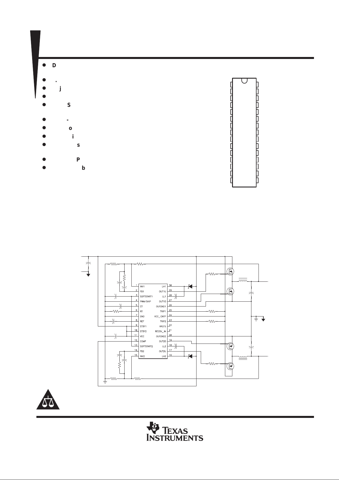
1
2
3
4
5
6
7
8
9
10
11
12
13
14
15
30
29
28
27
26
25
24
23
22
21
20
19
18
17
16
INV1
FB1
SOFTSTART1
PWM_SKIP
C
T
R
T
GND
REF
STBY1
STBY2
V
CC
COMP
SOFTSTART2
FB2
INV2
LH1
OUT1_u
LL1
OUT1_d
OUTGND1
TRIP1
VCC_CNTP
TRIP2
VREF5
REG5V_IN
OUTGND2
OUT2_d
LL2
OUT2_u
LH2
DBT PACKAGE
(TOP VIEW)
R6
R4
R2
R1
D2
C11
C9
C8
C6
C5
C2
U1
TPS5102DBT
G
ND
+
C1
C3
C4
C7
C10
D1
R3
R5
R7
5 V
Vo1
L1
Q1
R8
+
C12
Q4
R11
R10
R9
Q3
Q2
L2
Vo2
+
C13
TPS5102
DUAL, HIGH-EFFICIENCY CONTROLLER FOR NOTEBOOK PC POWER
SLVS239 - SEPTEMBER 1999
2
POST OFFICE BOX 655303 • DALLAS, TEXAS 75265
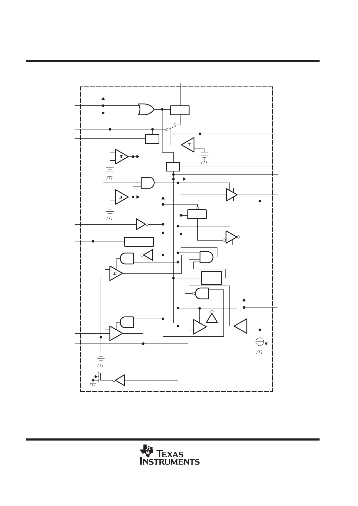
functional block diagram
To Channel 2
VREF5
_
+
4.5 V
_
+
REF
To
Channel 2
UVLO
3.8 V
OSC
To Channel 2
_
+
To
Channel 2
1.1 V
To
Channel 2
Sync.
Signal
1 Shot
SOFTSTART
_
+
Skip Comp
_
+
+
Error Amp
_
+
1.185 V
_
+
To
Channel 2
PWM Comp
STNBY2
REG5V_IN
V
CC
STNBY1
VREF5
REF
COMP
PWM/SKIP
SOFTSTART
INV
FB
RT
CT
LH
OUT_U
LL
OUT_D
OUTGND
VCC_CNTP
TRIP
1.185 V
TPS5102
DUAL, HIGH-EFFICIENCY CONTROLLER FOR NOTEBOOK PC POWER
SLVS239 - SEPTEMBER 1999
3
POST OFFICE BOX 655303 • DALLAS, TEXAS 75265
AVAILABLE OPTIONS
T
A
PACKAGE EVM
TSSOP(DBT)
–40°C to 85°C TPS5102IDBT TPS5102EVM-135
TPS5102IDBTR
Terminal Functions
TERMINAL
NAME NO.
I/O
DESCRIPTION
COMP 12 I/O Voltage monitor comparator input
C
T
5 I/O External capacitor connection for switching frequency adjustment
FB1 2 O CH1 error amp output
FB2 14 O CH2 error amp output
GND 7 Control GND
INV1 1 I CH1 inverting input
INV2 15 I CH2 inverting input
LH1 30 I/O CH1 boost capacitor connection
LH2 16 I/O CH2 boost capacitor connection
LL1 28 I/O CH1 boost circuit connection
LL2 18 I/O CH2 boost circuit connection
OUT1_d 27 I/O CH1 low-side gate-drive output
OUT2_d 19 O CH2 low-side gate-drive output
OUT1_u 29 O CH1 high-side drive output
OUT2_u 17 O CH2 high-side drive output
OUTGND1 26 Output GND 1
OUTGND2 20 Output GND 2
PWM_SKIP 4 I PWM/SKIP mode select
L:PWM mode H:SKIP mode
REF 8 O 1.185-V reference voltage output
REG5V_IN 21 I External 5-V input
R
T
6 I/O External resistor connection for switching frequency adjustment
SOFTSTAR T1 3 I/O External capacitor connection for CH1soft start timing.
SOFTSTAR T2 13 I/O External capacitor connection for CH2 soft start timing.
STBY1 9 I CH1 stand-by control
STBY2 10 I CH2 stand-by control
TRIP2 23 I External resistor connection for CH2 over current protection.
TRIP1 25 I External resistor connection for CH1 over current protection.
V
CC
11 Supply voltage input
V
ref
5 22 O 5-V internal regulator output
VCC_CNTP 24 I Supply voltage sense input

TPS5102
DUAL, HIGH-EFFICIENCY CONTROLLER FOR NOTEBOOK PC POWER
SLVS239 - SEPTEMBER 1999
4
POST OFFICE BOX 655303 • DALLAS, TEXAS 75265
detailed description
Vref (1.185 V)
The reference voltage is used to set the output voltage and the overvoltage protection (COMP).
Vref5 (5 V)
The internal linear voltage regulator is used for the high-side driver bootstrap voltage. Since the input voltage
range is from 4.5 V to 25 V, this feature offers a fixed voltage for the bootstrap voltage greatly simplifying the
drive design. It is also used for powering the low side driver. The tolerance is 6%.
5-V Switch
If the internal 5 V switch senses a 5-V input from REG5V_IN pin, the internal 5-V linear regulator will be
disconnected from the MOSFET drivers. The external 5 V will be used for both the low-side driver and the high
side bootstrap, thus increasing the efficiency.
PWM/SKIP
This pin is used to change between PWM and Skip mode. If the pin is lower than 0.5-V , the IC is in regular PWM
mode; if a minimum 2-V is applied to this pin, the IC works in Skip mode. In light load condition (<0.2 A), the
skip mode gives a short pulse to the low-side FET instead of a full pulse. By this control, switching frequency
is lowered, reducing switching loss; also the output capacitor energy discharging through the output inductor
and the low-side FET is prevented. Therefore, the IC can achieve high efficiency at light load conditions
(< 0.2 A).
err-amp
Each channel has its own error amplifier to regulate the output voltage of the synchronous-buck converter. It
is used in the PWM mode for the high output current condition (>0.2A). Voltage mode control is applied.
skip comparator
In Skip mode, each channel has its own hysteretic comparator to regulate the output voltage of the
synchronous-buck converter. The hysteresis is set internally and typically at 8.5 mV. The delay from the
comparator input to the driver output is typically 1.2 µs.
low-side driver
The low-side driver is designed to drive low-Rds(on) n-channel MOSFETs. The maximum drive voltage is 5 V
from Vref5. The current rating of the driver is typically 1 A, source and sink.
high-side driver
The high side driver is designed to drive low-Rds(on) n-channel MOSFETs. The current rating of the driver is
1 A, source and sink. When configured as a floating driver, the bias voltage to the driver is developed from V ref5,
limiting the maximum drive voltage between OUT_u and LL to 5 V. The maximum voltage that can be applied
between LHx and OUTGND is 30 V.
deadtime control
Deadtime prevents shoot–through current from flowing through the main power FETs during switching
transitions by actively controlling the turn-on time of the MOSFETs drivers. The typical deadtime from
low-side-driver-off to high-side-driver-on is 70 ns, and 85 ns from high-side-driver-off to low-side-driver-on.

TPS5102
DUAL, HIGH-EFFICIENCY CONTROLLER FOR NOTEBOOK PC POWER
SLVS239 - SEPTEMBER 1999
5
POST OFFICE BOX 655303 • DALLAS, TEXAS 75265
detailed description (continued)
current protection
Current protection is achieved by sensing the high-side power MOSFET drain-to-source voltage drop during
on-time at VCC_CNTP and LL. An external resistor between Vin and TRIP pin in serial with the internal current
source adjusts the current limit. When the voltage drop during the on-time is high enough, the current
comparator triggers the current protection and the circuit is reset. The reset repeats until the over-current
condition is removed.
COMP
COMP is an internal comparator used for any voltage protection such as the output under-voltage protection
for notebook power applications. If the core voltage is lower than the setpoint, the comparator turns off both
channels to prevent the notebook from damage.
SOFT1, SOFT2
Separate softstart terminals make it possible to set the start-up time of each output for any possibility.
STBY1, STBY2
Both channels can be switched into standby mode separately by grounding the STBY pin. The standby current
is as low as 1 µA.
ULVO
When the input voltage goes up to about 4 V, the IC is turned on, ready to function. When the input voltage is
lower than the turn-on value, the IC is turned off. The typical hysteresis is 40 mV.
TPS5102
DUAL, HIGH-EFFICIENCY CONTROLLER FOR NOTEBOOK PC POWER
SLVS239 - SEPTEMBER 1999
6
POST OFFICE BOX 655303 • DALLAS, TEXAS 75265
absolute maximum ratings over operating free-air temperature (unless otherwise noted)
†
Supply voltage, Vcc (see Note 1) -0.3 V to 27 V. . . . . . . . . . . . . . . . . . . . . . . . . . . . . . . . . . . . . . . . . . . . . . . . . . . .
Input voltage, INV -0.3 V to 7 V. . . . . . . . . . . . . . . . . . . . . . . . . . . . . . . . . . . . . . . . . . . . . . . . . . . . . . . . . . . . . . . . . .
SOFTSTART -0.3 V to 7 V. . . . . . . . . . . . . . . . . . . . . . . . . . . . . . . . . . . . . . . . . . . . . . . . . . . . . . . . . .
COMP -0.3 V to 6 V. . . . . . . . . . . . . . . . . . . . . . . . . . . . . . . . . . . . . . . . . . . . . . . . . . . . . . . . . . . . . . .
REG5_IN -0.3 V to 6 V. . . . . . . . . . . . . . . . . . . . . . . . . . . . . . . . . . . . . . . . . . . . . . . . . . . . . . . . . . . . .
STBY -0.3 V to 15 V. . . . . . . . . . . . . . . . . . . . . . . . . . . . . . . . . . . . . . . . . . . . . . . . . . . . . . . . . . . . . . .
Driver current 3 A. . . . . . . . . . . . . . . . . . . . . . . . . . . . . . . . . . . . . . . . . . . . . . . . . . . . . . . . . . . . . . . . .
TRIP -0.3 V to 27 V. . . . . . . . . . . . . . . . . . . . . . . . . . . . . . . . . . . . . . . . . . . . . . . . . . . . . . . . . . . . . . . .
C
T
-0.3 V to 7 V. . . . . . . . . . . . . . . . . . . . . . . . . . . . . . . . . . . . . . . . . . . . . . . . . . . . . . . . . . . . . . . . . . .
RT -0.3 V to 7 V. . . . . . . . . . . . . . . . . . . . . . . . . . . . . . . . . . . . . . . . . . . . . . . . . . . . . . . . . . . . . . . . . . .
LL -0.3 V to 27 V. . . . . . . . . . . . . . . . . . . . . . . . . . . . . . . . . . . . . . . . . . . . . . . . . . . . . . . . . . . . . . . . . .
LH -0.3 V to 32 V. . . . . . . . . . . . . . . . . . . . . . . . . . . . . . . . . . . . . . . . . . . . . . . . . . . . . . . . . . . . . . . . . .
OUT_u -0.3 V to 32 V. . . . . . . . . . . . . . . . . . . . . . . . . . . . . . . . . . . . . . . . . . . . . . . . . . . . . . . . . . . . . .
OUT_d -0.3 V to 7 V. . . . . . . . . . . . . . . . . . . . . . . . . . . . . . . . . . . . . . . . . . . . . . . . . . . . . . . . . . . . . . .
PWM/SKIP -0.3 V to 7 V. . . . . . . . . . . . . . . . . . . . . . . . . . . . . . . . . . . . . . . . . . . . . . . . . . . . . . . . . . .
VCC_Sense -0.3 V to 27V. . . . . . . . . . . . . . . . . . . . . . . . . . . . . . . . . . . . . . . . . . . . . . . . . . . . . . . . .
Power dissipation (T
A
= 25°C) 874 mW. . . . . . . . . . . . . . . . . . . . . . . . . . . . . . . . . . . . . . . . . . . . . . . . . . . . . . . . . . . .
Operating temperature (TA) -40°C to 85°C. . . . . . . . . . . . . . . . . . . . . . . . . . . . . . . . . . . . . . . . . . . . . . . . . . . . . . . . .
Operating temperature (TJ) -40°C to 125°C. . . . . . . . . . . . . . . . . . . . . . . . . . . . . . . . . . . . . . . . . . . . . . . . . . . . . . .
Storage temperature (T
STG)
-55°C to 150°C. . . . . . . . . . . . . . . . . . . . . . . . . . . . . . . . . . . . . . . . . . . . . . . . . . . . . .
†
Stresses beyond those listed under “absolute maximum ratings” may cause permanent damage to the device. These are stress ratings only, and
functional operation of the device at these or any other conditions beyond those indicated under “recommended operating conditions” is not
implied. Exposure to absolute-maximum-rated conditions for extended periods may affect device reliability.
NOTES: 1. All voltage values are with respect to the network ground terminal.
2. This rating is specified at duty ≤10% on output rise and fall each pulse. Each pulse width (rise and fall) for the peak current should
not exceed 2 µs.
3. See Dissipation Rating Table for free-air temperature range above 25°C.
DISSIPATION RATING TABLE
PACKAGE
TA ≤ 25°C
POWER RATING
DERATING FACTOR
ABOVE TA = 25°C
TA = 85°C
POWER RATING
DBT 874 mW 6.993 mW/°C 454 mW
recommended operating conditions
PARAMETERS MIN NOM MAX UNIT
Supply voltage, Vcc 4.5 25 V
INV1/2 CT RT, PWM/SKIP, SOFTSTART 6
p
5 V_IN -0.1 5.5
Input voltage, V
I
STBY1, STBY2 12
V
TRIP1/2 VCC_SENSE -0.1 25
C
T
100 pF
Oscillator frequency
R
T
82 kΩ
f
osc
PWM 200 KHz
Operation temperature range, T
A
-40 85 °C
TPS5102
DUAL, HIGH-EFFICIENCY CONTROLLER FOR NOTEBOOK PC POWER
SLVS239 - SEPTEMBER 1999
7
POST OFFICE BOX 655303 • DALLAS, TEXAS 75265
electrical characteristics over recommended operating free-air temperature range, VCC = 7 V
(unless otherwise noted)
reference voltage
PARAMETER TEST CONDITIONS MIN TYP MAX UNIT
TA = 25°C, I
vref
= 50 µA 1.167 1.185 1.203
Vref
Reference voltage
I
vref
= 50 µA 1.155 1.215
V
Regin Line regulation Vcc = 4.5, 25V, I = 50 µA 0.2 12 mV
Regl Load regulation I = 0.1 µA to 1 mA 0.5 10 mV
quiescent current
PARAMETER TEST CONDITIONS MIN TYP MAX UNIT
Icc Operating current without switching
Both STBY > 2.5 V ,
No switching, Vin = 4.5 – 25 V
0.6 1.5 mA
Iccs Stand-by current Both STBY < 0.5 V , Vin = 4.5 – 25 V 1 1000 nA
oscillator
PARAMETER TEST CONDITIONS MIN TYP MAX UNIT
fosc Frequency PWM operation 500 kHz
R
T
Timing resistor 56 kΩ
fdv
Vcc = 4.5 V to 25 V 0.1%
fdt
fosc change
TA = -40°C to 85°C 2%
p
DC, includes internal comparator error 1 1.1 1.2
V
oscH
H-level output voltage
Fosc = 200 kHz, Includes internal comparator error 1.17
V
p
Includes internal comparator error 0.4 0.5 0.6
V
oscL
L-level output voltage
Fosc = 200 kHz, Includes internal comparator error 0.43
V
error amp
PARAMETER TEST CONDITIONS MIN TYP MAX UNIT
Vio Input offset voltage TA = 25°C ±2 ±10 mV
Av Open-loop voltage gain 50 dB
GB Unity-gain bandwidth 0.8 MHz
Isnk Output sink current Vo = 0.4 V 30 45 µA
Isrc Output source current Vo = 1 V 300 µA
skip comparator
PARAMETER TEST CONDITIONS MIN TYP MAX UNIT
Vhys
†
Hysteresis window 6 9.5 13 mV
Vhoff Offset voltage 2 mV
Ihbias Bias current 10 pA
T
LHT
Propagation delay‡ from INV to OUTxU TTL input signal 0.7 µs
T
LH
10 mV overdrive on hysteresis band signal 1.2 µs
†
Vhys is assured by design.
‡
The total delay in the table includes the driver delay.
TPS5102
DUAL, HIGH-EFFICIENCY CONTROLLER FOR NOTEBOOK PC POWER
SLVS239 - SEPTEMBER 1999
8
POST OFFICE BOX 655303 • DALLAS, TEXAS 75265
electrical characteristics over recommended operating free-air temperature range, VCC = 7 V
(unless otherwise noted) (continued)
driver deadtime
PARAMETER TEST CONDITIONS MIN TYP MAX UNIT
T
DRVLH
Low side to high side 70 nS
T
DRVHL
High side to low side 85 nS
standby
PARAMETER TEST CONDITIONS MIN TYP MAX UNIT
V
IH
H-level input voltage
2.5
V
IL
L-level input voltage
STBY1, STBY2
0.5
V
T
turnon
Propagation delay
p
1.5
T
turnoff
Propagation delay
STBY to driver output
1.8
µ
s
5V regulator
PARAMETER TEST CONDITIONS MIN TYP MAX UNIT
V
O
Output voltage I = 10 mA 4.7 5.3 V
Regin Line regulation Vcc = 5.5 V, 25 V, I = 10 mA 20 mV
Regl Load regulation I = 1 V, 10 mA, Vcc = 5.5 V 40 mV
Ios Short-circuit output current Vref = 0 V 80 mA
5-V internal switch
PARAMETER TEST CONDITIONS MIN TYP MAX UNIT
V
TLH
4.2 4.8 V
V
THL
Threshold voltage
4.1 4.7 V
V
hys
Hysteresis 30 150 mV
UVLO
PARAMETER TEST CONDITIONS MIN TYP MAX UNIT
V
TLH
3.7 4.2 V
V
THL
Threshold voltage
3.6 4.1 V
V
hys
Hysteresis 10 40 150 mV
current limit
PARAMETER TEST CONDITIONS MIN TYP MAX UNIT
PWM mode 10 15 20
Internal current source
Skip mode 3 5 7
µ
A
Input offset voltage 2.5 mV
driver output
PARAMETER TEST CONDITIONS MIN TYP MAX UNIT
OUT_u sink current
0.5 1.2
OUT_d sink current
Vo
= 3
V
0.5 1.2
A
OUT_u source current
–1 –1.7
OUT_d source current
Vo
= 3
V
–1 –1.5
A
TPS5102
DUAL, HIGH-EFFICIENCY CONTROLLER FOR NOTEBOOK PC POWER
SLVS239 - SEPTEMBER 1999
9
POST OFFICE BOX 655303 • DALLAS, TEXAS 75265
electrical characteristics over recommended operating free-air temperature range, VCC = 7 V
(unless otherwise noted) (continued)
softstart
PARAMETER TEST CONDITIONS MIN TYP MAX UNIT
I
CTRL
Soft-start current 1.8 2.5 3 µA
Maximum discharge current 0.92 mA
V
TLH
p
3.4 3.9 4.7
V
THL
Threshold voltage (skip mode)
1.8 2.6 3.4
V
output voltage protection (COMP)
PARAMETER TEST CONDITIONS MIN TYP MAX UNIT
Threshold voltage 0.9 1.1 1.3 V
Progagation delay†, 50% duty cycle,
No capacitor on COMP or OUT_u pin,
Frequency = 200 kHz
Turnon 900 ns
Turnoff (with channel on) 400 ns
†
The delay time in the table includes the driver delay.
PWM/SKIP
PARAMETER TEST CONDITIONS MIN TYP MAX UNIT
High to low 0.5
Threshold
Low to high 2
V
High to low 550
Dela
y
Low to high 400
ns
TPS5102
DUAL, HIGH-EFFICIENCY CONTROLLER FOR NOTEBOOK PC POWER
SLVS239 - SEPTEMBER 1999
10
POST OFFICE BOX 655303 • DALLAS, TEXAS 75265
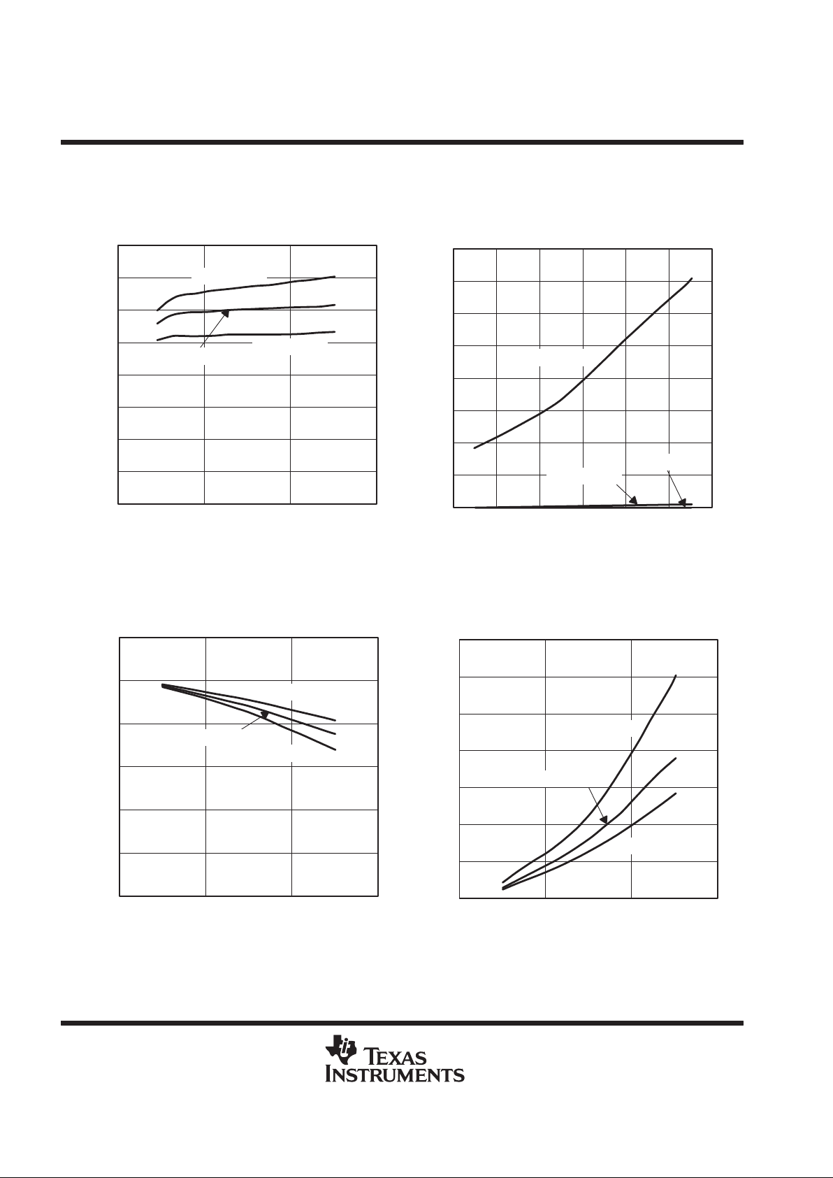
TYPICAL CHARACTERISTICS
Figure 1
500
300
100
0
010
IQ – Quiescent Current –
600
700
QUIESCENT CURRENT (BOTH CHANNELS ON)
vs
INPUT VOLTAGE
800
20 30
400
200
Aµ
VCC - Supply Voltage - V
TJ = 125°C
TJ = 25°C
TJ = -40°C
Figure 2
TJ = 25°C
TJ = -40°C
TJ = 125°C
100
80
40
0
4.5 7 10 15
– Quiescent Current – nA
120
140
160
20 25
60
20
I
Off
VCC - Supply Voltage - V
QUIESCENT CURRENT (BOTH CHANNELS STANDBY)
vs
INPUT VOLTAGE
Figure 3
3
2
1
0
0.1 0.5
– Driver Output Voltage – V
4
5
DRIVE CURRENT (SOURCE)
vs
DRIVE VOLTAGE
6
1
I
(src)
- Driver Source Current - A
V
(src)
TJ = 25°C
TJ = -40°C
TJ = 125°C
Figure 4
2
1.5
1
0
0.1 0.5
– Driver Output Voltage – V
2.5
3
DRIVE CURRENT (SINK)
vs
DRIVE VOLTAGE
3.5
1
0.5
V
(snk)
I
(snk)
- Driver Sink Current - A
TJ = 25°C
TJ = -40°C
TJ = 125°C

TPS5102
DUAL, HIGH-EFFICIENCY CONTROLLER FOR NOTEBOOK PC POWER
SLVS239 - SEPTEMBER 1999
11
POST OFFICE BOX 655303 • DALLAS, TEXAS 75265
TYPICAL CHARACTERISTICS
Figure 5
TJ = 25°C
TJ = -40°C
TJ = 125°C
4.7
4.6
4.4
4.2
010
– Source Current –
5
5.1
CURRENT PROTECTION SOURCE CURRENT
(SKIP MODE)
vs
INPUT VOLTAGE
5.2
20 30
4.9
4.8
4.5
4.3
VCC - Supply Voltage - V
I
(protec)
Aµ
Figure 6
13.4
13
12.8
12.6
4.5 7 10 15
13.6
13.8
14
20 25
13.2
VCC - Supply Voltage - V
– Source Current –
I
(trip)
Aµ
CURRENT PROTECTION SOURCE CURRENT
(PWM MODE)
vs
INPUT VOLTAGE
TJ = 25°C
TJ = -40°C
TJ = 125°C
Figure 7
TJ = 25°C
TJ = -40°C
TJ = 125°C
0.5
0.3
0.2
0
010
– Threshold Voltage – V
0.8
0.9
PWM/SKIP THRESHOLD VOLTAGE
vs
INPUT VOLTAGE
1
20 30
0.7
0.6
0.4
0.1
VI - Supply Voltage - V
V
T
Figure 8
TJ = 25°C
TJ = -40°C
TJ = 125°C
4.8
4.7
4.6
4.5
0 –10 –20 –30
– Voltage – V
4.9
5
V
ref5
VOLTAGE
vs
CURRENT
5.1
–40 –50
Ir - Current - mA
V
ref5

TPS5102
DUAL, HIGH-EFFICIENCY CONTROLLER FOR NOTEBOOK PC POWER
SLVS239 - SEPTEMBER 1999
12
POST OFFICE BOX 655303 • DALLAS, TEXAS 75265
TYPICAL CHARACTERISTICS
Figure 9
1
0.5
0
110
Maximum Output Voltage
1.5
2
Switching Frequency – kHz
MAXIMUM OUTPUT VOLTAGE
vs
SWITCHING FREQUENCY
2.5
100 1000
Figure 10
TJ - Junction Temperature - °C
–1.5
–1
–0.5
0
–40 –20 0 25 50 70 95
Soft Start Charge Current
–2
–2.5
SOFT START CHARGE CURRENT
vs
JUNCTION TEMPERATURE
–3
125
Figure 11
Timing Resistor - kΩ
Ct = 47 pF
Ct = 100 pF
Ct = 150 pF
Ct = 220 pF
Ct = 330 pF
100
10
10 100
Switching Frequency
SWITCHING FREQUENCY
vs
TIMING RESISTOR
1000
1000

TPS5102
DUAL, HIGH-EFFICIENCY CONTROLLER FOR NOTEBOOK PC POWER
SLVS239 - SEPTEMBER 1999
13
POST OFFICE BOX 655303 • DALLAS, TEXAS 75265
TYPICAL CHARACTERISTICS
timing diagram
1.17 V Typ.
0.43 V Typ.
High
Low
High
Low
High
Low
IL = 0
GND
-Vf
Detected Over Current
Current Limit
TRIPx Voltage
Duty
Delay
(100 nS Typ.)
Delay
(100 nS Typ.)
Err. Amplifier Output
Oscillator Output
OUTx_u
OUTx_d
Over-Current
Protection
Inductor Current
LLx Voltage

TPS5102
DUAL, HIGH-EFFICIENCY CONTROLLER FOR NOTEBOOK PC POWER
SLVS239 - SEPTEMBER 1999
14
POST OFFICE BOX 655303 • DALLAS, TEXAS 75265
APPLICATION INFORMATION
The design shown in this application report is a reference design for notebook applications. An evaluation
module (EVM), TPS5102EVM-135 (SLVP135), is available for customer testing and evaluation. The intent is
to allow a customer to fully evaluate the given design using the plug-in EVM supply shown here. For subsequent
customer board revisions, the EVM design can be copied onto the users’ PCB to shorten design cycle.
The following key design procedures will aid in the design of the notebook power supply using the TPS5102:
TP4
TP3
TP2
TP1
C7
R6
R4
R3
C6
TP27
SLVP135 EVM
TP22
TP23
TP24
C17
D3
Q1
TP26
R17
Q2
TP18
C21
TP16
TP17
TP21
TP20
TP19
TP25
Q3
C20
D4
Q4
R20
R21
C18
R18
R19
C19
TP28
C16
R16
R15
R11
TP5
TP6
TP7
TP8
TP9
TP10
C14
TP11
TP12
TP13
TP14
TP15
R12
JP2
JP1
R10
R8
C12
C13
C15
C10
R9
C11
R14
R13
C9
R5
C8
D1
C2
L1
+
C4
R1
+
C22
J1
RS1
J2
Vo1
J3
Vo1
J4
Vo1GND
+
C5
D2
J16
GND
J15
GND
+
C23
+
C1
J5
Vo1GND
J6
Vin
J7
Vin
J8
Input GND
J9
Input GND
J10
Vo2GND
J11
Vo2GND
J12
Vo2
J13
Vo2
J14
RS2
R2
L2
C3
Vin Iin Vo1 Io1 Vo2 Io2
6 V to 15 V 6 A 3.3 V 4 A 5 V 4 A
16 V to 25 V 3.3 V 2.5 A 5 V 2.5 A
output voltage setpoint calculation
The output voltage is set by the reference voltage and the voltage divider. In the TPS5102, the reference voltage
is 1.185-V , and the divider is composed of two resistors in the EVM design that are R4 and R5, or R14 and R15.
The equation for the setpoint is:
R
2
+
R
1
Vr
Vo–Vr
Where R1 is the top resistor (kΩ) ( R4 or R15); R2 is the bottom resistor (kΩ) ( R5 or R14); Vo is the required
output voltage (V); Vr is the reference voltage (1.185 V in TPS5102).
Example: R1 = 1 kΩ; Vr = 1.185 V; Vo = 3.3 V, then R2 = 560 Ω.
Some of the most popular output voltage setpoints are calculated in the table below:
V
O
1.3 V 1.5 V 1.8 V 2.5 V 3.3 V 5 V
R1 (top) (kΩ) 1 V 1 V 1 V 1 V 1 V 1 V
R2 (bottom) (kΩ) 10 V 3.7 V 1.9 V 0.9 V 0.56 V 0.31 V

TPS5102
DUAL, HIGH-EFFICIENCY CONTROLLER FOR NOTEBOOK PC POWER
SLVS239 - SEPTEMBER 1999
15
POST OFFICE BOX 655303 • DALLAS, TEXAS 75265
APPLICATION INFORMATION
output voltage setpoint calculation (continued)
If a higher precision resistor is used, the voltage setup can be more accurate.
In some applications, the output voltage is required to be lower than the reference voltage. With a few extra
components, the lower voltage can be easily achieved. The drawing below shows the method.
TPS5102
V
CC
V
O
R
(top)
R
(bottom)
R
z1
Zener
INV
R
z2
In the schematic, the Rz1, the Rz2, and the zener are the extra components. Rz1 is used to give the zener
enough current to build up the zener voltage. The zener voltage is added to INV through Rz2. Therefore, the
voltage on the INV is still equal to the IC internal voltage (1.185 V) even if the output voltage is regulated at a
lower setpoint. The equation for setting up the output voltage is shown below:
Rbtm
Vr
Rtop
)VoVr(
)VrVz(
2Rz
+
–
–
=
When Rz2 is the adjusting resistor for low output voltage; Vz is the zener voltage; Vr is the internal reference
voltage; Rtop is the resistor of the voltage sensing network; Rbtm is the bottom resistor of the sensing
network;VO is the required output voltage setpoint.
Example: Assuming the required output voltage setpoint is VO = 0.8 V , VZ = 5 V; Rtop = 1 kΩ; Rbottom = 1 kΩ,
Then the Rz2 = 2.43 kΩ.
output inductor ripple current
The output inductor current ripple can affect not only the efficiency, but also the output voltage ripple. The
equation is exhibited below:
Iripple
+
Vin*Vout*Iout
(
Rdson)R
L
)
Lout
D
Ts
Where
Iripple
is the peak-to-peak ripple current (A) through the inductor;
Vin
is the input voltage (V);
Vout
is the
output voltage (V);
Iout
is the output current;
Rdson
is the on-time resistance of MOSFET (Ω); D is the duty cycle;
and Ts is the switching cycle (S). From the equation, it can be seen that the current ripple can be adjusted by
changing the output inductor value.
Example: Vin = 5 V; Vout = 1.8 V; Iout = 5 A; Rdson = 10 mΩ; RL = 5 mΩ; D = 0.36; Ts = 10 µS; Lout = 6 µH
Then, the ripple Iripple = 2 A.

TPS5102
DUAL, HIGH-EFFICIENCY CONTROLLER FOR NOTEBOOK PC POWER
SLVS239 - SEPTEMBER 1999
16
POST OFFICE BOX 655303 • DALLAS, TEXAS 75265
APPLICATION INFORMATION
output capacitor RMS current
Assuming the inductor ripple current totally goes through the output capacitor to ground, the RMS current in the
output capacitor can be calculated as:
Iorms
+
D
I
12
Ǹ
Where
Io(rms)
is the maximum RMS current in the output capacitor (A); ∆I is the peak-to-peak inductor ripple
current (A).
Example: ∆I = 2 A, so Io(rms) = 0.58 A
input capacitor RMS current
Assuming the input ripple current totally goes into the input capacitor to the power ground, the RMS current in
the input capacitor can be calculated as:
Iirms
+
Io
2
D
(1–D)
)
1
12
D Iripple
2
Ǹ
Where
Ii(rms
) is the input RMS current in the input capacitor (A); Io is the output current (A); Iripple is the
peak-to-peak output inductor ripple current;
D
is the duty cycle. From the equation, it can be seen that the
highest input RMS current usually occurs at the lowest input voltage, so it is the worst case design for input
capacitor ripple current.
Example: Io = 5 A; D = 0.36; Iripple = 2 A,
Then, Ii(rms) = 2.42 A
soft-start
The soft-start timing can be adjusted by selecting the soft-start capacitor value. The equation is
C
soft
+2
T
soft
Where
C
soft
is the soft-start capacitance (µF) (C9 or C13 in EVM design); T
soft
is the start-up time (S).
Example: Tsoft = 5 mS, so Csoft = 0.01 µF.

TPS5102
DUAL, HIGH-EFFICIENCY CONTROLLER FOR NOTEBOOK PC POWER
SLVS239 - SEPTEMBER 1999
17
POST OFFICE BOX 655303 • DALLAS, TEXAS 75265
APPLICATION INFORMATION
current protection
The current limit in TPS5102 on each channel is set using an internal current source and an external resistor
(R18 or R19). The sensed high side MOSFET drain-to-source voltage drop is compared to the set point, if the
voltage drop exceeds the limit, the internal oscillator is activated, and it continuously reset the current limit until
the over-current condition is removed. The equation below should be used for calculating the external resistor
value for current protection setpoint:
Rcl
+
Rds(on
) (
Itrip)Iind(p-p
)ń2)
0.000015
In skip mode,
Rcl
+
Rds(on
) (
Itrip)Iind(p-p
)ń2)
0.000005
Where Rcl is the external current limit resistor (R10 or R11); Rds(on) is the high side MOSFET (Q1 or Q3)
on-time resistance. Itrip is the required current limit; Iind(p-p) is the peak-to-peak output inductor current.
Example for voltage mode: Rds(on) = 10 mΩ, Itrip = 5 A, Iind = 2 A, so Rcl = 4 kΩ.
loop-gain compensation
Voltage mode control is used in this controller for the output voltage regulation. To achieve fast, stabilized
control, two parts are discussed in this section: the power stage small signal modeling and the compensation
circuit design.
For the buck converter, the small signal modeling circuit is shown below:
+
-
ac
i
a
i
c
p
D
1
V
ap
D
d
∧
Ic d
∧
+
V
I
R
L
L
Z
L
C
R
R
C
Z
RC
V
O
From this equivalent circuit, several control transfer functions can be derived: input-to-output, output
impedance, and control-to-output. Typically the control-to-output transfer function is used for the feedback
control design.
Assuming Rc and RL are much smaller than R, the simplified small signal control-to-output transfer function is:
Vod
+
Vo
d
+
(1
)
sCRc
)
1
)
sƪC
ǒ
Rc)R
L
Ǔ
)
L
R
ƫ
)
s2LC
∧
∧
Where C is the output capacitance; Rc is the equivalent serial resistance (ESR) in the output capacitor; L is the
output inductor; RL is the equivalent serial resistance (DCR) in the output inductor; R is the load resistance.

TPS5102
DUAL, HIGH-EFFICIENCY CONTROLLER FOR NOTEBOOK PC POWER
SLVS239 - SEPTEMBER 1999
18
POST OFFICE BOX 655303 • DALLAS, TEXAS 75265
APPLICATION INFORMATION
loop-gain compensation (continued)
T o achieve fast transient response and the better output voltage regulation, a compensation circuit is added to
improve the feedback control. The whole system is shown:
PWM
Power
Stage
Compensation
V
ref
The typical compensation circuit used as an option in the EVM design is a part of the output feedback circuit.
The circuitry is displayed below:
_
+
R4
C3
C2
R2R1
C1
R3
V
ref
To PWM
This circuit is composed of one integrator, two poles, and two zeros:
Assuming R1 << R2 and C2 << C3, the equation is:
Comp
+
(
1
)sC3R4) (1
)sC2R2
)
sC3R
2(1
)sC2R4)(1
)sC1R1
)
Therefore,
Pole
1
+
1
2
pC1R1
Zero
1
+
1
2
pC2R2
Pole
2
+
1
2
pC2R4
Zero
2
+
1
2
pC3R4
Integrator
+
1
2
pC3R2
A simplified version used in the EVM design is exhibited below:

TPS5102
DUAL, HIGH-EFFICIENCY CONTROLLER FOR NOTEBOOK PC POWER
SLVS239 - SEPTEMBER 1999
19
POST OFFICE BOX 655303 • DALLAS, TEXAS 75265
APPLICATION INFORMATION
loop-gain compensation (continued)
_
+
R4
C3
C2
R2
R3
V
ref
To PWM
V
O
Assuming C2 << C3, the equation is:
Comp
+
(
1
)sC3R4
)
sC3R
2(1
)sC2R4
)
There is one pole, one zero and one integrator:
Zero
+
1
2
pC3R4
Pole
+
1
2
pC2R4
Integrator
+
1
2
pfC3R2
The loop-gain concept is used to design a stable and fast feedback control. The loop-gain equation is derived
by the control-to-output transfer function times the compensation:
Loop–gain+Vod Comp
The amplitude and the phase of this equation can be drawn with software such as MathCad. In turn, the stability
can be easily designed by adjusting the compensation parameters. The sample bode plot is shown below to
explain the phase margin, gain margin, and the crossover frequency.
The gain is drawn as 20 log (loop-gain), and the phase is in degrees. To explain them clearer, 180 degrees is
added to the phase, so that the gain and phase share the same zero.
The crossover frequency is the point at which the gain curve touches zero. The higher this frequency , the faster
the transient response, since the transient recovery time is 1/(crossover frequency). The phase is the phase
margin. The phase margin should be at least 60 degrees to cover all changes such as temperature. The gain
margin is the gap between the gain curve and the zero when the phase curve touches zero. This margin should
be at least 20 dB to guarantee stability over all conditions.

TPS5102
DUAL, HIGH-EFFICIENCY CONTROLLER FOR NOTEBOOK PC POWER
SLVS239 - SEPTEMBER 1999
20
POST OFFICE BOX 655303 • DALLAS, TEXAS 75265
APPLICATION INFORMATION
Phase
Margin
Phase
Gain
Crossover
Gain
Margin
54
–2
–44
–100
96
166
f – Frequency – Hz
180
152
138
124
110
82
68
40
26
12
–16
–30
–58
–72
–86
10 100 10
3
10
4
10
5
10
6
20 Log (Loop-Gain)
180 + Phase
synchronization
Some applications require switching clock synchronization. There are two methods that can be used for
synchronization: the triangle wave synchronization and the square wave synchronization.
The triangle wave synchronization is displayed below:
740 mV
740 mV
Ct
Rt
TPS5102
It can be seen that both Rt and Ct are removed from the circuit. Therefore, two components are saved. This
method is good for the synchronization between two controllers. If the controller needs to be synchronized with
a digital circuit such as DSP, the square-type clock signal is usually used. The configuration exhibited below is
for this type of application:

TPS5102
DUAL, HIGH-EFFICIENCY CONTROLLER FOR NOTEBOOK PC POWER
SLVS239 - SEPTEMBER 1999
21
POST OFFICE BOX 655303 • DALLAS, TEXAS 75265
APPLICATION INFORMATION
synchronization (continued)
Ct
Rt
TPS5102
An external resistor is added into the circuit, but Rt is still removed. Ct is kept to be a part of RC circuit generating
triangle waveform for the controller. Assuming the peak value of the square is known, the resistor and the
capacitor can be adjusted to achieve the correct peak-to-peak value and the offset value.
layout guidelines
Good power supply results will only occur when care is given to proper design and layout. Layout will affect noise
pickup and generation and can cause a good design to perform with less than expected results. With a range
of currents from milliamps to tens or even hundreds of amps, good power supply layout is much more difficult
than most general PCB designs. The general design should proceed from the switching node to the output,
then back to the driver section and, finally , parallel the low-level components. Below are several specific points
to consider
before
the layout of a TPS5102 design begins.
D
All sensitive analog components should be referenced to ANAGND. These include components connected
to Vref5, Vref, INV, LH, and COMP .
D
Analog ground and drive ground should be isolated as much as possible. Ideally , analog ground will connect
to the ground side of the bulk storage capacitors on VO, and drive ground will connect to the main ground
plane close to the source of the low-side FET.
D
Connections from the drivers to the gate of the power FETs should be as short and wide as possible to
reduce stray inductance. This becomes more critical if external gate resistors are not being used.
D
The bypass capacitor for VCC should be placed close to the TPS5102.
D
When configuring the high-side driver as a floating driver, the connection from LL to the power FETs should
be as short and as wide as possible.
D
When configuring the high-side driver as a floating driver, the bootstrap capacitor (connected from LH to
LL) should be placed close to the TPS5102.
D
When configuring the high-side driver as a ground-referenced driver, LL should be connected to DR VGND.
D
The bulk storage capacitors across VIn should be placed close to the power FETS. High-frequency bypass
capacitors should be placed in parallel with the bulk capacitors and connected close to the drain of the
high-side FET and to the source of the low-side FET.
D
High-frequency bypass capacitors should be placed across the bulk storage capacitors on VO.
D
LH and LL should be connected very close to the drain and source, respectively , of the high-side FET. LH
and LL should be routed very close to each other to minimize differential-mode noise coupling to these
traces.
D
The output voltage sensing trace should be isolated by either ground trace or Vcc trace.

TPS5102
DUAL, HIGH-EFFICIENCY CONTROLLER FOR NOTEBOOK PC POWER
SLVS239 - SEPTEMBER 1999
22
POST OFFICE BOX 655303 • DALLAS, TEXAS 75265
APPLICATION INFORMATION
Figure 12
IO - Output Current - A
80
75
70
60
0 0.2 0.4 0.6
Efficiency – %
85
90
PWM AND SKIP MODE EFFICIENCY
COMPARISON
95
0.8 1 1.2
65
PWM Mode
Skip Mode
Output = 3.3 V
Figure 13
Skip Mode
PWM Mode
80
75
70
60
0 0.2 0.4 0.6
90
95
100
0.8 1 1.2
85
65
IO - Output Current - A
Efficiency – %
Output = 5 V
PWM AND SKIP MODE EFFICIENCY
COMPARISON
Figure 14
PWM Mode
Skip Mode
Output = 3.3 V
85
75
65
60
0123
90
95
100
45
80
70
IO - Output Current - A
Efficiency – %
EFFICIENCY
vs
OUTPUT CURRENT
Figure 15
Skip Mode
PWM Mode
Output = 5 V
85
75
65
60
0123
90
95
100
45
80
70
IO - Output Current - A
Efficiency – %
EFFICIENCY
vs
OUTPUT CURRENT

TPS5102
DUAL, HIGH-EFFICIENCY CONTROLLER FOR NOTEBOOK PC POWER
SLVS239 - SEPTEMBER 1999
23
POST OFFICE BOX 655303 • DALLAS, TEXAS 75265
APPLICATION INFORMATION
Figure 16
Dual Output Efficiency
85
75
65
60
0204060
Efficiency – %
90
95
Output Current – %
EFFICIENCY
vs
OUTPUT CURRENT
100
80 100
80
70
Figure 17
3.32
3.28
3.26
3.2
0123
– Output Voltage – V
3.34
3.38
OUTPUT LOAD REGULATION
3.4
45
3.36
3.3
3.24
3.22
V
O
IO - Output Current - A
Output Load = 3.3 V
Figure 18
5.04
4.98
4.94
4.9
0123
5.06
5.08
5.1
45
5.02
5
4.96
4.92
– Output Voltage – V
V
O
IO - Output Current - A
Output Load = 5 V
OUTPUT LOAD REGULATION
Figure 19
VI - Input Voltage - V
3.34
3.28
3.24
3.2
010
3.36
3.38
3.4
20 30
3.32
3.3
3.26
3.22
– Output Voltage – V
V
O
Output Line = 3.3 V
OUTPUT LINE REGULATION

TPS5102
DUAL, HIGH-EFFICIENCY CONTROLLER FOR NOTEBOOK PC POWER
SLVS239 - SEPTEMBER 1999
24
POST OFFICE BOX 655303 • DALLAS, TEXAS 75265
APPLICATION INFORMATION
Figure 20
5.05
5.04
5.02
5
5101520
5.08
5.09
5.1
25 30
5.07
5.06
5.03
5.01
VI - Input Voltage - V
– Output Voltage – V
V
O
Output Line = 5 V
OUTPUT LINE REGULATION
Figure 21
80
75
65
60
0123
85
90
95
45
70
Output Diode Version = 3.3 V
IO - Output Current - A
Efficiency – %
DIODE VERSION EFFICIENCY
Figure 22
3.3–V OUTPUT VOLTAGE RIPPLE
Figure 23
5–V OUTPUT VOLTAGE RIPPLE

TPS5102
DUAL, HIGH-EFFICIENCY CONTROLLER FOR NOTEBOOK PC POWER
SLVS239 - SEPTEMBER 1999
25
POST OFFICE BOX 655303 • DALLAS, TEXAS 75265
APPLICATION INFORMATION
Table 1. Bill of Materials
REF. PN DESCRIPTION MANUFACTURER SIZE
C1 RV-35V221MH10-R Capacitor, electrolytic, 220 µF, 35 V ELNA 10x10mm
C1†opt 10TPB220M Capacitor, POSCAP, 220 µF, 10 V Sanyo 7.3x4.3mm
C2 GMK325F106ZH Capacitor, ceramic, 10 µF, 35 V Taiyo Yuden 1210
C3 GMK325F106ZH Capacitor, ceramic, 10 µF, 35 V Taiyo Yuden 1210
C4 4TPB470M Capacitor , POSCAP, 470 µF, 4 V Sanyo 7.3x4.3mm
C5 10TPB220M Capacitor, POSCAP, 220 µF, 10 V Sanyo 7.3x4.3mm
C5†opt 6TPB330M Capacitor, POSCAP, 330 µF, 6.3 V Sanyo 7.3x4.3mm
C6
†
Standard Open, capacitor, ceramic, 0.22 µF, 16 V 805
C7 Standard Capacitor, ceramic, 0,01 µF, 16 V 805
C8 Standard Capacitor, ceramic, 220 pF, 16 V 805
C9 Standard Capacitor, ceramic, 0.01 µF, 16 V 805
C10 Standard Capacitor, ceramic, 100 pF, 16 V 805
C11 Standard Capacitor, ceramic, 1 µF, 16 V muRata 805
C12 GMK316F225ZG Capacitor , ceramic, 2.2 µF, 35 V Taiyo Yuden 1206
C13 Standard Capacitor, ceramic, 0.01 µF, 16 V 805
C14 Standard Capacitor, ceramic, 220 pF, 16 V 805
C15 Standard Capacitor, ceramic, 0.1 µF, 16 V 805
C16
†
Standard Open, capacitor, ceramic, 0.1 µF, 16 V 805
C17 GMK316F225ZG Capacitor , ceramic, 2.2 µF, 35 V Taiyo Yuden 1206
C18 Standard Open 805
C19 Standard Open 805
C20 GMK325F106ZH Capacitor, ceramic, 10 µF, 35 V Taiyo Yuden 1210
C21 GMK316F225ZG Capacitor , ceramic, 2.2 µF, 35 V Taiyo Yuden 1206
C22
†
7.3x4.3mm
C23
†
7.3x4.3mm
D1 MBRS340T3 Diode, Schottky , 40 V, 3 A Motorola SMC
D2 MBRS340T3 Diode, Schottky , 40 V, 3 A Motorola SMC
D3 SD103-AWDICT-ND Diode, Schottky, 40 V, 200 mA Digikey 3.5x1.5mm
D4 SD103-AWDICT-ND Diode, Schottky, 40 V, 200 mA Digikey 3.5x1.5mm
L1 DO3316P-682 Inductor , 6.8 µH, 4.4 A Coilcraft 0.5x0.37in
L2 DO3316P-682 Inductor , 6.8 µH, 4.4 A Coilcraft 0.5x0.37in
J1-J16 CA26DA-D36W-OFC Edge connector, surface mount, 0.040” board, 0.090”
standoff
NAS Interplex 0.040in
JP1 S1132-2-ND Header, straight, 2-pin, 0.1 ctrs, 0.3” pins Sullins DigiKey # 1 132-2-ND
JP1 shunt S1132-14-ND Shunt, jumper, 0.1” Sullins DigiKey #
929950-00-ND
JP2 S1132-14-ND Header, straight, 2-pin, 0.1 ctrs, 0.3” pins Sullins DigiKey # 1132-2-ND
R1 Standard Resistor, 5.1 Ω, 5% 805
R2 Standard Resistor, 5.1 Ω, 5% 805
R3
†
Standard Open 805
R4 Standard Resistor, 1.21 kΩ, 1% 805
R5 Standard Resistor, 680 Ω, 1% 805
R6 Standard Resistor, 5.1 kΩ, 5% 805
R8 Standard Resistor, 1 kΩ, 5% 805
†
Option table

TPS5102
DUAL, HIGH-EFFICIENCY CONTROLLER FOR NOTEBOOK PC POWER
SLVS239 - SEPTEMBER 1999
26
POST OFFICE BOX 655303 • DALLAS, TEXAS 75265
APPLICATION INFORMATION
Table 1. Bill of Materials (continued)
REF. PN DESCRIPTION MANUFACTURER SIZE
R9 Standard Resistor, 82 kΩ, 5% 805
R10 Standard Resistor, 1 kΩ, 5% 805
R11 Standard Resistor, 0 Ω, 5% 805
R12 Standard Resistor, 1 kΩ, 5% 805
R13 Standard Reistor, 1 kΩ, 5% 805
R14 Standard Resistor, 310 kΩ, 1% 805
R15 Standard Resistor, 1 kΩ, 1% 805
R16
†
Standard Open resistor, 5.1 Ω, 5% 805
R17 Standard Resister, 15 Ω, 5% 805
R18 Standard Resistor, 7.5 kΩ, 5% 805
R19 Standard Resistor, 7.5 kΩ, 5% 805
R20 Standard Resistor, 15 Ω, 5% 805
R21 Standard Open 805
Q1 Si4410DY Transistor, MOSFET, n-ch, 30 V , 10 A, 13 mΩ, Siliconix SO-8
Q2 Si4410DY Transistor, MOSFET, n-ch, 30 V , 10 A, 13 mΩ, Siliconix SO-8
Q3 Si4410DY Transistor, MOSFET, n-ch, 30 V , 10 A, 13 mΩ, Siliconix SO-8
Q4 Si4410DY Transistor, MOSFET, n-ch, 30 V , 10 A, 13 mΩ, Siliconix SO-8
U1 TPS5102 IC, Dual Controller TI TSSOP
†
Option table
This EVM is designed to cover as many applications as possible. For some more specific applications, the circuit
can be simpler. The table below gives some recommendations.
Table 2. EVM Application Recommendations
5V INPUT VOLTAGE <3–A OUTPUT CURRENT DIODE VERSION
Change C1 to low profile capacitor
Sanyo 10TPB220M (220 µF, 10 V)
Or 6TPB330M (330 µF, 6.3 V)
Change Q1/Q2 and Q3/Q4 to dual pack MOSFET, IRF7311 to reduce the cost.
Remove Q2 and Q4 to reduce the cost.
Remove R12
Table 3. Vendor and Source Information
MATERIAL SOURCE PART NUMBER DISTRIBUTORS
MOSFETS (Q1–Q4)
In EVM Design Si4410DY (SILICONIX)
Local Distributor
()
Second Source IRF7811 (International Rectifier)
INPUT CAPACITORS (C1) In EVM Design RV–35V221MH10–R (ELNA) Bell Microproducts
972–783–4191
Second Source 35CV330AX/GX (Sanyo) 870–633–5030
UUR1V221MNR1GS (Nichicon) Future Electronics (Local Office)
MAIN DIODES (D1 – D2) In EVM Design MBRS340T3 (Motorola) Local Distributors
Second Source U3FWJ44N (Toshiba) Local Distributors
INDUCTORS (L1 – L2) In EVM Design DO3316P–682 (Coilcraft) 972–248-3575
Second Source CTDO3316P–682 (Inductor Warehouse) 800–533–8295
CERAMIC CAPACITORS
(C2, C3) (C12, C17, C21)
IN EVM Design GMK325F106ZH
GMK316F225ZG
(Taiyo Yuden)
SMEC
512–331–1877
Taiyo Yuden, Representative e–mail: mike@millsales.com

TPS5102
DUAL, HIGH-EFFICIENCY CONTROLLER FOR NOTEBOOK PC POWER
SLVS239 - SEPTEMBER 1999
27
POST OFFICE BOX 655303 • DALLAS, TEXAS 75265
APPLICATION INFORMATION
Top Layer
Bottom Layer (Top V iew)
Top Assembly

TPS5102
DUAL, HIGH-EFFICIENCY CONTROLLER FOR NOTEBOOK PC POWER
SLVS239 - SEPTEMBER 1999
28
POST OFFICE BOX 655303 • DALLAS, TEXAS 75265
APPLICATION INFORMATION
Load
+
–
0 – 4 A
+
–
Power Supply
5–V, 5–A Supply
Load
0 – 4 A
NOTE: All wire pairs should be twisted.
Test Setup

TPS5102
DUAL, HIGH-EFFICIENCY CONTROLLER FOR NOTEBOOK PC POWER
SLVS239 - SEPTEMBER 1999
29
POST OFFICE BOX 655303 • DALLAS, TEXAS 75265
APPLICATION INFORMATION
High current applications are described in table . The values are recommendations based on actual test circuits.
Many variations are possible based on the requirements of the user. Performance of teh circuit is dependent
upon the layout rather than the on specific components, if the device parameters are not exceeded. The power
stage, having the highest current levels and greatest dv/dt rates, should be given the most attention, as both
the supply and load can be severly affected by the power levels and edge rates.
Table 4. High Current Applications
REFERENCE
DESIGNATIONS
FUNCTION 8-A OUTPUT 12-A OUTPUT 16-A OUTPUT
C1 Input Bulk Capacitor
2x ELNA
RV-35V221MH10-R
220 µF, 35 V
3x ELNA
RV-35V221MH10-R
220 µF, 35 V
4x ELNA
RV-35V221MH10-R
220 µF, 35 V
C2 (C3) Input Bypass Capacitor
2x Taiyo Yuden
GMK325F106ZH
10 µF, 35 V
3x Taiyo Yuden
GMK325F106ZH
10 µF, 35 V
4x Taiyo Yuden
GMK325F106ZH
10 µF, 35 V
L1 (L2) Output Filter Indicator
Coiltronics UP3B-2R2
2.2 µH, 9.2 A
Coiltronics UP4B-1R5
1.5 µH, 13.4 A
MicorMetals T68-8/90
Core w/7T, #16
1.0 µH, 25 A
C4 (C22) Output Filter Capacitor
2x Sanyo 4TPB470M
470 µF, 4 V
3x Sanyo 4TPB470M
470 µF, 4 V
4x Sanyo 4TPB470M
470 µF, 4 V
C5 (C23) Output Filter Capacitor
2x Sanyo 6TPB330M
330 µF, 6.3 V
3x Sanyo 6TPB330M
330 µF, 6.3 V
4x Sanyo 6TPB330M
330 µF, 6.3 V
Q1 (Q3) Power Switch
2x Siliconix Si4410DY
30 V , 10 A, 13 mΩ
3x Siliconix Si4410DY
30 V , 10 A, 13 mΩ
4x Siliconix Si4410DY
30 V , 10 A, 13 mΩ
Q2 (Q4) Power Switch
2x Siliconix Si4410DY
30 V , 10 A, 13 mΩ
3x Siliconix Si4410DY
30 V , 10 A, 13 mΩ
4x Siliconix Si4410DY
30 V , 10 A, 13 mΩ
R17 (R20) Gate Drive Resistor 7 Ω 5 Ω 4 Ω
R18 (R19) Current Limit Resistor 10 kΩ 15 kΩ 20 kΩ
Switching Frequency 200 kHz 150 kHz 100 kHz

TPS5102
DUAL, HIGH-EFFICIENCY CONTROLLER FOR NOTEBOOK PC POWER
SLVS239 - SEPTEMBER 1999
30
POST OFFICE BOX 655303 • DALLAS, TEXAS 75265
DBT (R-PDSO-G**) PLASTIC SMALL-OUTLINE PACKAGE
30 PINS SHOWN
0,75
0,25
0,50
0,15 NOM
Gage Plane
50
12,60
38
9,80 11,10
44
12,409,60 10,90
4073252/D 09/97
4,30
4,50
0,27
0,17
16
15
30
A
1
7,90
30
DIM
A MAX
PINS **
7,70
A MIN
1,20 MAX
6,60
6,20
Seating Plane
0,10
0,50
M
0,08
0°-8°
7,90
28
7,70
0,15
0,05
NOTES: A. All linear dimensions are in millimeters.
B. This drawing is subject to change without notice.
C. Body dimensions do not include mold flash or protrusion.
D. Falls within JEDEC MO-153

IMPORTANT NOTICE
T exas Instruments and its subsidiaries (TI) reserve the right to make changes to their products or to discontinue
any product or service without notice, and advise customers to obtain the latest version of relevant information
to verify, before placing orders, that information being relied on is current and complete. All products are sold
subject to the terms and conditions of sale supplied at the time of order acknowledgement, including those
pertaining to warranty, patent infringement, and limitation of liability.
TI warrants performance of its semiconductor products to the specifications applicable at the time of sale in
accordance with TI’s standard warranty. Testing and other quality control techniques are utilized to the extent
TI deems necessary to support this warranty. Specific testing of all parameters of each device is not necessarily
performed, except those mandated by government requirements.
CERT AIN APPLICATIONS USING SEMICONDUCTOR PRODUCTS MAY INVOLVE POTENTIAL RISKS OF
DEATH, PERSONAL INJURY, OR SEVERE PROPERTY OR ENVIRONMENTAL DAMAGE (“CRITICAL
APPLICATIONS”). TI SEMICONDUCTOR PRODUCTS ARE NOT DESIGNED, AUTHORIZED, OR
WARRANTED TO BE SUITABLE FOR USE IN LIFE-SUPPORT DEVICES OR SYSTEMS OR OTHER
CRITICAL APPLICATIONS. INCLUSION OF TI PRODUCTS IN SUCH APPLICA TIONS IS UNDERSTOOD T O
BE FULLY AT THE CUSTOMER’S RISK.
In order to minimize risks associated with the customer’s applications, adequate design and operating
safeguards must be provided by the customer to minimize inherent or procedural hazards.
TI assumes no liability for applications assistance or customer product design. TI does not warrant or represent
that any license, either express or implied, is granted under any patent right, copyright, mask work right, or other
intellectual property right of TI covering or relating to any combination, machine, or process in which such
semiconductor products or services might be or are used. TI’s publication of information regarding any third
party’s products or services does not constitute TI’s approval, warranty or endorsement thereof.
Copyright 1999, Texas Instruments Incorporated
 Loading...