

TPS5100
TRIPLE-CHANNEL PWM CONTROL CIRCUITS
SLVS169 – JANUARY 2000
1
POST OFFICE BOX 655303 • DALLAS, TEXAS 75265
D
Low Voltage Operation . . . 2.5 V to 7 V
D
Low Power . . . 3. 5 mA
(f = 500 kHz, Duty = 50%)
D
Internal Undervoltage Lockout Protection
D
Internal Short Circuit Protection
D
Wide Operating Frequency . . . 50 kHz to
1 MHz
D
Internal Precision Reference . . . 1.25 V ±1%
(25°C)
D
On/Off Switch for CH1/3 Pair and Ch2 (see
Function Table)
D
0 to 100% Dead Time Control
D
Totem Pole Output Stage
D
Smal l Package . . . 16 Pin TSSOP
description
The TPS5100 is a triple PWM control circuit, primarily designed to compose the power supply for LCD display .
Each PWM channel has own error amplifier, PWM comparator, dead-time control and output driver. The
trimmed voltage reference, oscillator, undervoltage lockout and short circuit protection are common for all
channels.
This device includes two boost exclusive circuits (ch1,3) and a buck-boost exclusive circuit (ch2). The operating
frequency is set with external resister and capacitor, and dead time is continuously adjustable form 0% to 100%
duty cycle with resistive divider network. Soft start function can be implemented by adding a capacitor to dead
time divider network. Two dead time control inputs are assigned for ch1,3 pair and ch2 individually and each
dead time control input can be used to control on/off operation. TPS5100 can operate from 2.5 V supply voltage
and ch1,3 pair and ch2 operate with reverse phase switching each other to achieve efficient operation in low
power and battery powered system.
The TPS5100 is characterized for operation from –20°C to 85°C.
FUNCTION TABLE
OUTPUT
CONDITION
CH-1 CH-2 CH-3
DTC1/3 >. 0.3 V , DTC2 > 0.3 V ON H ON L ON H
DTC1/3 > 0.3 V , DTC2 <. 0.2 V ON H OFF H ON H
DTC1/3 < 0.2 V , DTC2 > 0.3 V OFF L ON L OFF L
DTC1/3 < 0.2 V , DTC2 < 0.2 V OFF L OFF H OFF L
AVAILABLE OPTIONS
PACKAGE
T
A
TSSOP
(PW)
–20°C to 85°C TPS5100PW
Copyright 2000, Texas Instruments Incorporated
PRODUCTION DATA information is current as of publication date.
Products conform to specifications per the terms of Texas Instruments
standard warranty. Production processing does not necessarily include
testing of all parameters.
Please be aware that an important notice concerning availability, standard warranty, and use in critical applications of
Texas Instruments semiconductor products and disclaimers thereto appears at the end of this data sheet.
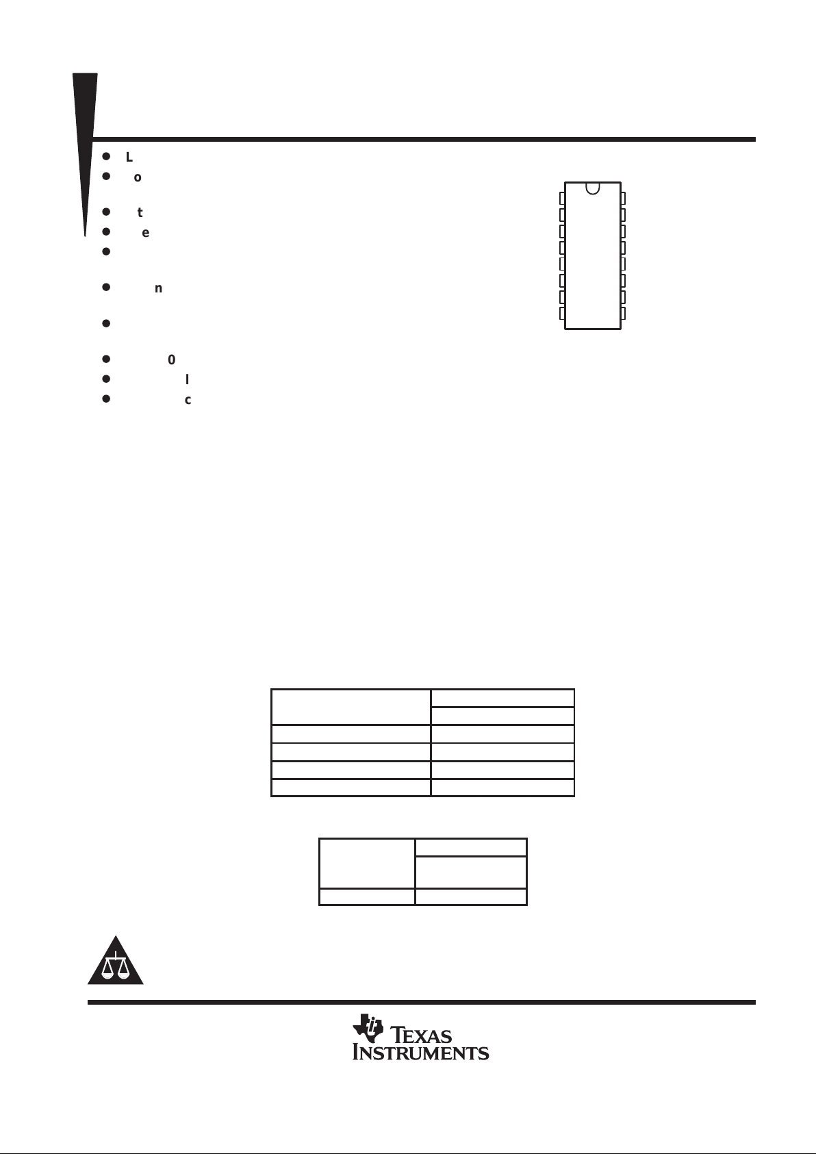
1
2
3
4
5
6
7
8
16
15
14
13
12
11
10
9
IN-2
E/O2
V
CC
OUT2
OUT3
OUT1
GND
SCP
E/O3
IN-3
IN-1
E/O1
C
T/RT
DTC2
DTC1/3
V
REF
PW PACKAGE
(TOP VIEW)
TPS5100
TRIPLE-CHANNEL PWM CONTROL CIRCUITS
SLVS169 – JANUARY 2000
2
POST OFFICE BOX 655303 • DALLAS, TEXAS 75265
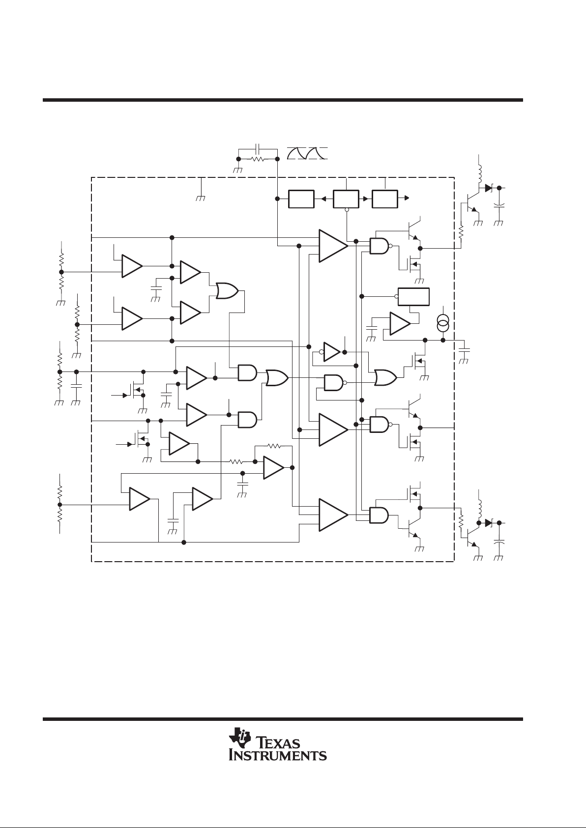
functional block diagram
_
+
_
+
+
–
_
+
+
–
_
+
_
+
_
+
_
+
+
–
–
+
–
+
–
+
+
–
+
+
–
1 V
0.4 V
V
01
V
03
V
ref
V
ref
–V
O2
E/01
IN–1
IN–3
E/03
DTC1/3
DTC2
IN–2
E/02
DIS
DIS
V
ref
V
ref
E/A1
E/C1
E/A3
E/C3
V
T2
1.15 V
VT1, 0.25 V
EN1
EN2
R
R
VT4, 0.7 V
VT3, 0.25 V
E/C2
E/A2
GND
OSC
CT/R
T
UVLO
V
CC
V
ref
V
ref
To Internal
Circuitry
V
CC
PWM/C
PWM/C
PWM/C
DIS
EN1
EN1
EN2
V
T5
1.25 V
LATCH
SPC/C
2 µA
V
CC
V
CC
V
CC
OUT1
OUT3
OUT2
SCP
V
CC
V
01
V
CC
–V
O2
Boost
Buck-Boost
NOTE A: All voltages and currents listed are nominal.
TPS5100
TRIPLE-CHANNEL PWM CONTROL CIRCUITS
SLVS169 – JANUARY 2000
3
POST OFFICE BOX 655303 • DALLAS, TEXAS 75265
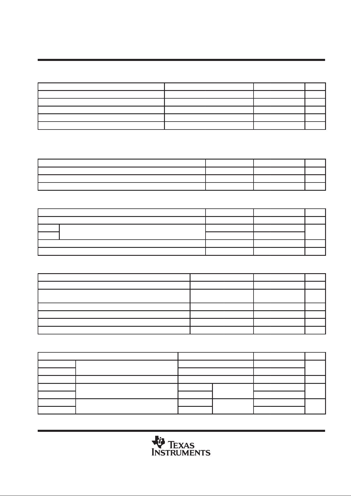
electrical characteristics over recommended operating free-air temperature range, VCC = 3.3 V
(unless otherwise noted) (see Note 1)
PARAMETER TEST CONDITIONS MIN TYP MAX UNIT
V
REF
Reference voltage I
REF
= –1 mA, TA = 25°C 1.237 1.250 1.263 V
V
REF(dev)
Reference voltage change with T
A
I
REF
= –1 mA, See Note 2 15 25 mV
R
EGIN
Input regulation I
REF
= –1 mA, VCC = 2.5 V to 7 V 2 5 mV
R
EGL
Output regulation I
REF
= –0.1 mA to –1 mA 1 5 mV
I
OS
Short-circuit output current V
REF
= 0 –2 –10 –30 mA
NOTES: 1. Typical values of all parameters except for V
REF(dev)
and fdT are specified at TA = 25°C.
2. The deviation parameter V
REF(dev)
is defined as the difference between the maximum and minimum values obtained over the
recommended free-air temperature range (–20°C to 85°C).
undervoltage lockout section
PARAMETER TEST CONDITIONS MIN TYP MAX UNIT
V
TH
Upper threshold voltage TA = 25°C 2.2 2.3 2.4 V
V
TL
Lower threshold voltage TA = 25°C 2 2.1 2.2 V
V
hys
Hysteresis (VTH – VTL) TA = 25°C 0.1 0.2 0.3 V
NOTE 1: Typical values of all parameters except for V
REF(dev)
and fdT are specified at TA = 25°C.
protection control section
PARAMETER TEST CONDITIONS MIN TYP MAX UNIT
I
SCP
Input terminal source current –1.4 –2 –2.6 µA
V
T2
p
CH-1, 3 1.10 1.15 1.20
V
T3
Input threshold voltage
CH-2 0.20 0.25 0.30
V
V
R
Latch reset threshold voltage TA = 25°C 0.8 1.5 V
V
T5
Threshold voltage 1.20 1.25 1.30 V
NOTE 1: Typical values of all parameters except for V
REF(dev)
and fdT are specified at TA = 25°C.
oscillator section
PARAMETER TEST CONDITIONS MIN TYP MAX UNIT
f
OSC
Frequency CT = 130 pF, RT = 7 kΩ 400 500 600 kHz
f
dV
Frequency change with V
CC
VCC = 2.5 V,
CT = 130 pF,
TA = 25°C,
RT = 7 kΩ
1% 2%
f
dT
Frequency change with T
A
CT = 130 pF, RT = 7 kΩ 5% 10%
I
CT/RT
Output source current –180 –200 –220 µA
V
OSCH
H level output voltage 0.95 1 1.05 V
V
OSCL
L level output voltage 0.35 0.40 0.45 V
NOTE 1: Typical values of all parameters except for V
REF(dev)
and fdT are specified at TA = 25°C.
dead time control section
PARAMETER TEST CONDITIONS MIN TYP MAX UNIT
I
BDT1/3
p
V
DTC1/3
= 0.35 V to 1.05 V 200
I
BDT2
Input bias current
V
DTC2
= 0.35 V to 1.05 V ±2 ±20
nA
V
T1
Comparator threshold voltage 0.2 0.25 0.3 V
V
T0(DTC1/3)
p
Duty = 0%
0.3 0.4 0.5
V
T100(DTC1/3)
Input threshold voltage (DTC1/3) (see Note 3)
Duty = 100%
f
OSC
=
500 kH
z
0.9 1 1.1
V
V
T0(DTC2)
p
Duty = 0%
0.3 0.4 0.5
V
T100(DTC2)
Input threshold voltage (DTC2) (see NOte 3)
Duty = 100%
f
OSC
=
500 kH
z
0.9 1 1.1
V
NOTES: 1: Typical values of all parameters except for V
REF(dev)
and fdT are specified at TA = 25°C.
3. These specifications are not production tested. They are specified as ensured values on circuit design.
TPS5100
TRIPLE-CHANNEL PWM CONTROL CIRCUITS
SLVS169 – JANUARY 2000
4
POST OFFICE BOX 655303 • DALLAS, TEXAS 75265
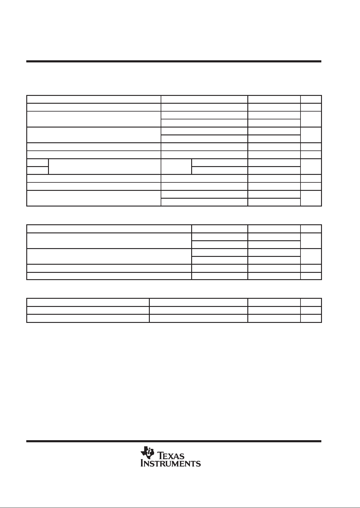
electrical characteristics over recommended operating free-air temperature range, VCC = 3.3 V
(unless otherwise noted) (see Note 1) (continued)
error amplifier section
PARAMETER TEST CONDITIONS MIN TYP MAX UNIT
V
IO
Input offset voltage CH1, 3, Av = 1 15 mV
p
CH1, 3, VI = –.95 V to 1.55 V ±10 ±20
IIBInput bias current
CH2, VI = 0.4 V to 1 V ±10 ±20
nA
p
CH1, 3, 0.95 1.55
VIRInput voltage range
CH2 0.4 1
V
A
VD
Open-loop voltage amplification RFB = 200 kΩ 60 dB
B
1
Unity-gain bandwidth 1 MHz
V
OM+
p
IO = 60 µA 1.2
V
OM–
Output voltage swing
V
ID
= 0.1
V
IO = 0.2 mA 0.2
V
I
OM+
Output sink current VID = 0.1 V, VO = 0.2 V 0.2 1 mA
I
OM–
Output source current VID = 0.1 V, VO = 1.2 V –60 –100 µA
p
CH2, AV = 1, TA = 25°C 678 700 722
VT4Input bias voltage
CH2, AV = 1 665 700 735
mV
NOTE 1: Typical values of all parameters except for V
REF(dev)
and fdT are specified at TA = 25°C.
output section
PARAMETER TEST CONDITIONS MIN TYP MAX UNIT
p
IO = 20 mA (CH2) 2.9 3.05
VOHHigh-level output voltage
IO = –40 mA (CH1, 3) 1.9 2.2 2.6
V
p
IO = 20 mA (CH1, 3) 0.2 0.4
VOLLow-level output voltage
IO = 40 mA (CH2) 0.2 0.3 0.6
V
t
r
Rise time CL = 1000 pF 130 ns
t
f
Fall time IO = 1000 pF 50 ns
NOTE 1: Typical values of all parameters except for V
REF(dev)
and fdT are specified at TA = 25°C.
total device
PARAMETER TEST CONDITIONS MIN TYP MAX UNIT
I
CC
Supply current Output OFF state 2.5 4 mA
I
CCA
Average supply current F
OSC
= 500 kHz, Duty = 50%, No load 3.5 5 mA
NOTE 1: Typical values of all parameters except for V
REF(dev)
and fdT are specified at TA = 25°C.

TPS5100
TRIPLE-CHANNEL PWM CONTROL CIRCUITS
SLVS169 – JANUARY 2000
5
POST OFFICE BOX 655303 • DALLAS, TEXAS 75265
TYPICAL CHARACTERISTICS
Figure 1
REFERENCE VOLTAGE
vs
FREE-AIR TEMPERATURE
–50 0 100 150
TA – Free-Air Temperature – °C
50
VCC = 3.3 V
IO = –1 mA
1.26
1.24
1.22
1.27
1.25
1.23
V
ref
– Reference Voltage – V
Figure 2
INPUT THRESHOLD VOLTAGE (UVLO)
vs
FREE-AIR TEMPERATURE
–50 0 100 150
TA – Free-Air Temperature – °C
50
VCC = 3.3 V
2.4
2.2
2
2.5
2.3
2.1
– Input Threshold Voltage (UVLO) – V
V
IT
Figure 3
SUPPLY CURRENT
vs
FREE-AIR TEMPERATURE
–50 0 100 150
TA – Free-Air Temperature – °C
50
VCC = 3.3 V
4
2
0
5
3
1
I
CC
– Supply Current – mA
I
CCA
I
CC
Figure 4
SOURCE CURRENT
vs
FREE-AIR TEMPERATURE
–50 0 100 150
TA – Free-Air Temperature – °C
50
VCC = 3.3 V
–2.2
–2.6
–1.8
–2
–2.4
I – Source Current –
S
Aµ

TPS5100
TRIPLE-CHANNEL PWM CONTROL CIRCUITS
SLVS169 – JANUARY 2000
6
POST OFFICE BOX 655303 • DALLAS, TEXAS 75265
TYPICAL CHARACTERISTICS
Figure 5
OSCILLATOR FREQUENCY
vs
TIMING CAPACITOR
10 100 10000
CT – Timing Capacitor – pF
1000
10k
1k
100
10
f
OSC
– Oscillator Frequency – kHz
VCC = 3.3 V
RT = 6.8 kΩ
TA = 25°C
Figure 6
OSCILLATOR FREQUENCY
vs
FREE-AIR TEMPERATURE
–50 0 100 150
TA – Free-Air Temperature – °C
50
490
480
505
495
485
500
VCC = 3.3 V
RT = 6.8 kΩ
CT = 130 pF
f
OSC
– Oscillator Frequency – kHz
SOURCE CURRENT
vs
FREE-AIR TEMPERATURE
–50 0 100 150
TA – Free-Air Temperature – °C
50
–200
–210
–190
–195
–205
I – Source Current –
S
Aµ
VCC = 3.3 V
ICT/I
RT
Figure 7

TPS5100
TRIPLE-CHANNEL PWM CONTROL CIRCUITS
SLVS169 – JANUARY 2000
7
POST OFFICE BOX 655303 • DALLAS, TEXAS 75265
TYPICAL CHARACTERISTICS
Figure 8
INPUT THRESHOLD VOLTAGE (DTC)
vs
TIMING CAPACITOR
10 100 10000
f
OSC
– Oscillator Frequency – kHz
1000
1.04
1.02
0
0.98
VCC = 3.3 V
RT = 6.8 kΩ
TA = 25°C
V
IT
– Input Threshold Voltage – V
Figure 9
INPUT THRESHOLD VOLTAGE (DTC)
vs
TIMING CAPACITOR
10 100 10000
f
OSC
– Oscillator Frequency – kHz
1000
0.42
0.4
0.38
0.36
VCC = 3.3 V
RT = 6.8 kΩ
TA = 25°C
V
IT
– Input Threshold Voltage – V
Figure 10
OUTPUT VOLTAGE
vs
FREE-AIR TEMPERATURE
–50 0 100 150
TA – Free-Air Temperature – °C
50
2.5
1.5
3.5
3
2
VCC = 3.3 V
– Output Voltage – V
V
O
IO = 40 mA
IO = 20 mA
Figure 11
OUTPUT VOLTAGE
vs
FREE-AIR TEMPERATURE
–50 0 100 150
TA – Free-Air Temperature – °C
50
0.2
0
0.4
0.3
0.1
VCC = 3.3 V
IO = 20 mA
IO = 40 mA
– Output Voltage – V
V
O

TPS5100
TRIPLE-CHANNEL PWM CONTROL CIRCUITS
SLVS169 – JANUARY 2000
8
POST OFFICE BOX 655303 • DALLAS, TEXAS 75265
TYPICAL CHARACTERISTICS
Figure 12
MAXIMUM PEAK OUTPUT VOLTAGE
vs
OUTPUT SOURCE CURRENT
–50 0 100 150
IOM – Output Source Current – µA
50
2
0
3
1
VCC = 3.3 V
TA = 25°C
– Maximum Peak Output Voltage – V
V
OM
Figure 13
OUTPUT VOLTAGE
vs
SUPPLY VOLTAGE
02 68
VCC – Supply Voltage – V
4
4
0
8
6
2
– Output Voltage – V
V
O
IO = 60 µA
TA = 25°C
Figure 14
OUTPUT VOLTAGE
vs
OUTPUT CURRENT
0 0.5 1.5 2
IO – Output Current – mA
1
100
0
200
150
50
– Output Voltage – mV
V
O
VCC = 3.3 V
TA = 25°C
Figure 15
VCC – Supply Voltage – V
REFERENCE VOLTAGE
vs
SUPPLY VOLTAGE
1.2
0.8
0.4
0
0.5 1.5
1.4
1
0.6
0.2
12 30
2.5
V
ref
– PWM Reference Voltage – V
TA = 25°C
Fall
Rise

TPS5100
TRIPLE-CHANNEL PWM CONTROL CIRCUITS
SLVS169 – JANUARY 2000
9
POST OFFICE BOX 655303 • DALLAS, TEXAS 75265
TYPICAL CHARACTERISTICS
Figure 16
OPEN-LOOP GAIN
vs
FREQUENCY
40
20
0
–40
0.1 10
f – Frequency – kHz
–20
1 100 1000
60
80
0.01
Open-Loop Gain – dB
10k
VCC = 3.3 V
TA = 25°C
Rf = 390 kΩ
Figure 17
PHASE SHIFT
vs
FREQUENCY
–45
–90
–135
–225
0.1 10
f – Frequency – kHz
–180
1 100 1000
0
0.01
Phase Shift – degrees
10k
VCC = 3.3 V
Inv-Amp
Rf = 390 kΩ
TA = 25°C

TPS5100
TRIPLE-CHANNEL PWM CONTROL CIRCUITS
SLVS169 – JANUARY 2000
10
POST OFFICE BOX 655303 • DALLAS, TEXAS 75265
MECHANICAL DATA
PW (R-PDSO-G**) PLASTIC SMALL-OUTLINE PACKAGE
4040064/E 08/96
14 PIN SHOWN
Seating Plane
1,20 MAX
1
A
7
14
0,19
4,50
4,30
8
6,20
6,60
0,30
0,75
0,50
0,25
Gage Plane
0,15 NOM
0,65
M
0,10
0°–8°
0,10
PINS **
A MIN
A MAX
DIM
2,90
3,10
8
4,90
5,10
14
6,60
6,404,90
5,10
16
7,70
20
7,90
24
9,60
9,80
28
0,15
0,05
NOTES: A. All linear dimensions are in millimeters.
B. This drawing is subject to change without notice.
C. Body dimensions do not include mold flash or protrusion not to exceed 0,15.
D. Falls within JEDEC MO-153

IMPORTANT NOTICE
T exas Instruments and its subsidiaries (TI) reserve the right to make changes to their products or to discontinue
any product or service without notice, and advise customers to obtain the latest version of relevant information
to verify, before placing orders, that information being relied on is current and complete. All products are sold
subject to the terms and conditions of sale supplied at the time of order acknowledgement, including those
pertaining to warranty, patent infringement, and limitation of liability.
TI warrants performance of its semiconductor products to the specifications applicable at the time of sale in
accordance with TI’s standard warranty. Testing and other quality control techniques are utilized to the extent
TI deems necessary to support this warranty. Specific testing of all parameters of each device is not necessarily
performed, except those mandated by government requirements.
CERT AIN APPLICATIONS USING SEMICONDUCT OR PRODUCTS MAY INVOLVE POTENTIAL RISKS OF
DEATH, PERSONAL INJURY, OR SEVERE PROPERTY OR ENVIRONMENTAL DAMAGE (“CRITICAL
APPLICATIONS”). TI SEMICONDUCTOR PRODUCTS ARE NOT DESIGNED, AUTHORIZED, OR
WARRANTED TO BE SUITABLE FOR USE IN LIFE-SUPPORT DEVICES OR SYSTEMS OR OTHER
CRITICAL APPLICATIONS. INCLUSION OF TI PRODUCTS IN SUCH APPLICA TIONS IS UNDERSTOOD T O
BE FULLY AT THE CUSTOMER’S RISK.
In order to minimize risks associated with the customer’s applications, adequate design and operating
safeguards must be provided by the customer to minimize inherent or procedural hazards.
TI assumes no liability for applications assistance or customer product design. TI does not warrant or represent
that any license, either express or implied, is granted under any patent right, copyright, mask work right, or other
intellectual property right of TI covering or relating to any combination, machine, or process in which such
semiconductor products or services might be or are used. TI’s publication of information regarding any third
party’s products or services does not constitute TI’s approval, warranty or endorsement thereof.
Copyright 2000, Texas Instruments Incorporated
 Loading...