Texas Instruments TPS40210, TPS40210DRCT Datasheet
1
2
3
4
10
9
8
7
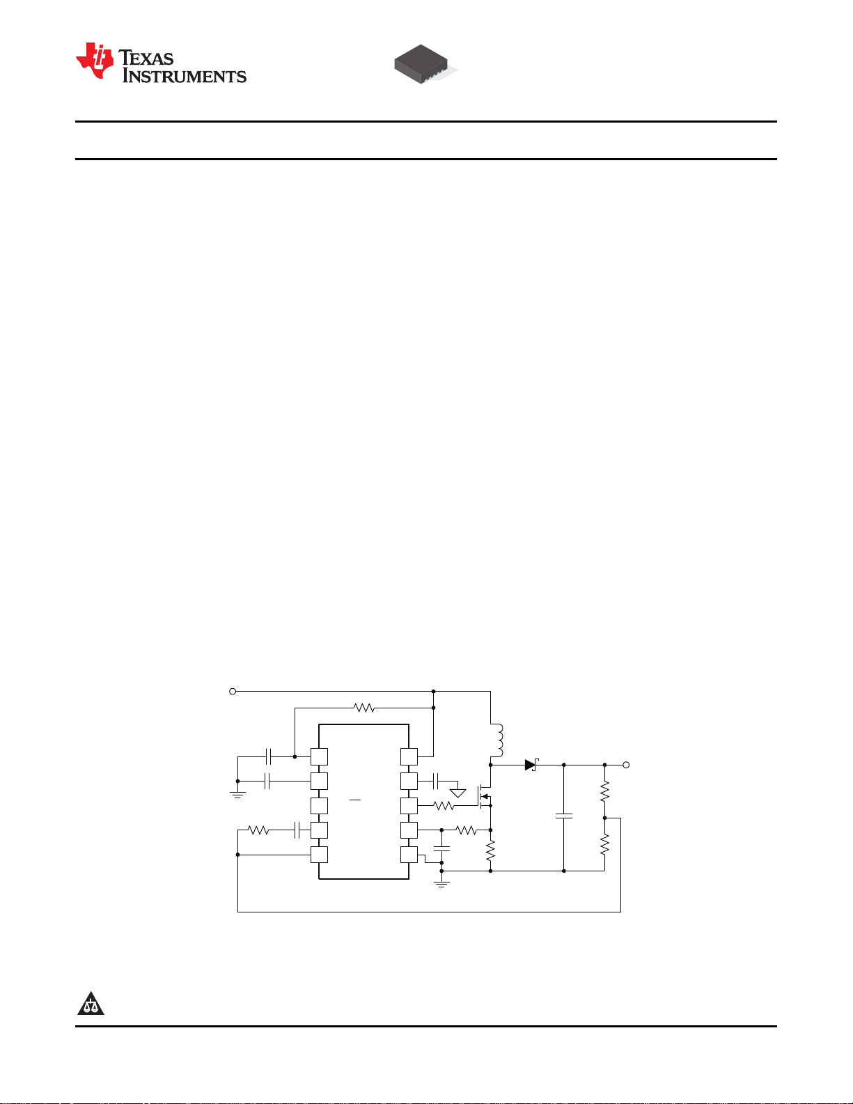
RC
DIS/EN
COMP
SS
VDD
ISNS
GDRV
GND
TPS40210
V
OUT
V
IN
5 FB 6
BP
R
SENSE
UDG-07110
TPS40210 , TPS40211
www.ti.com
.......................................................................................................................................................... SLUS772B – MARCH 2008 – REVISED JUNE 2008
4.5-V TO 52-V INPUT CURRENT MODE BOOST CONTROLLER
1
FEATURES CONTENTS
• For Boost, Flyback, SEPIC, LED Drive Apps
• Wide Input Operating Voltage: 4.5 V to 52 V
• Adjustable Oscillator Frequency
• Fixed Frequency Current Mode Control
• Internal Slope Compensation
• Integrated Low-Side Driver
• Programmable Closed Loop Soft Start
• Overcurrent Protection
• External Synchronization Capable
• Reference700-mV (TPS40210), 260-mV
(TPS40211)
• Low Current Disable Function
APPLICATIONS
• LED Lighting
• Industrial Control Systems
• Battery Powered Systems
Device Ratings 2
Electrical Characteristics 3
Typical Characteristics 5
Terminal Information 10
Application Information 12
Additional References 25
Design Examples 26
DESCRIPTION
The TPS40210 and TPS40211 are wide-input voltage
(4.5 V to 52 V), non-synchronous boost controllers.
They are suitable for topologies which require a
grounded source N-channel FET including boost,
flyback, SEPIC and various LED Driver applications.
The device features include programmable soft start,
overcurrent protection with automatic retry and
programmable oscillator frequency. Current mode
control provides improved transient response and
simplified loop compensation. The main difference
between the two parts is the reference voltage to
which the error amplifier regulates the FB pin.
1
Please be aware that an important notice concerning availability, standard warranty, and use in critical applications of Texas
Instruments semiconductor products and disclaimers thereto appears at the end of this data sheet.
PRODUCTION DATA information is current as of publication date.
Products conform to specifications per the terms of the Texas
Instruments standard warranty. Production processing does not
necessarily include testing of all parameters.
Copyright © 2008, Texas Instruments Incorporated
TPS40210 , TPS40211
SLUS772B – MARCH 2008 – REVISED JUNE 2008 ..........................................................................................................................................................
These devices have limited built-in ESD protection. The leads should be shorted together or the device placed in conductive foam
during storage or handling to prevent electrostatic damage to the MOS gates.
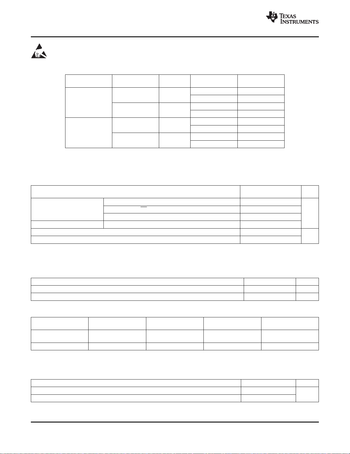
ORDERING INFORMATION
T
J
-40 ° C to 125 ° C
-40 ° C to 125 ° C
PACKAGE PART NUMBER
10-Pin MSOP
PowerPAD
10-Pin SON DRC
10-Pin MSOP
PowerPAD
10-Pin SON DRC
PACKAGE TAPE AND REEL
LEAD QUANTITY
DGQ
DGQ
2500 TPS40210DGQR
80 TPS40210DGQ
3000 TPS40210DRCR
250 TPS40210DRCT
2500 TPS40211DGQR
80 TPS40211DGQ
3000 TPS40211DRCR
250 TPS40211DRCT
DEVICE RATINGS
ABSOLUTE MAXIMUM RATINGS
over operating free-air temperature range unless otherwise noted
VDD – 0.3 to 52
Input voltage range RC, SS, FB, DIS/ EN – 0.3 to 10
ISNS – 0.3 to 8
Output voltage range COMP, BP, GDRV – 0.3 to 9
T
T
(1) Stresses beyond those listed under " absolute maximum ratings " may cause permanent damage to the device. These are stress ratings
Operating junction temperature range – 40 to 150
J
Storage temperature – 55 to 150
stg
only, and functional operation of the device at these or any other conditions beyond those indicated under " recommended operating
conditions " is not implied. Exposure to absolute-maximum-rated conditions for extended periods may affect device reliability.
(1)
TPS40210
TPS40211
www.ti.com
UNIT
V
° C
RECOMMENDED OPERATING CONDITIONS
MIN NOM MAX UNIT
V
T
Input voltage 4.5 52 V
VDD
Operating Junction temperature -40 125 ° C
J
PACKAGE DISSIPATION RATINGS
R
High-K Board
PACKAGE AIRFLOW (LFM)
10-Pin MSOP PowerPAD 0 (Natural Convection) 57.7 1.73 0.693
(DGQ)
10-Pin SON (DRC) 0 (Natural Convection) 47.9 2.08 0.835
(1) Ratings based on JEDEC High Thermal Conductivity (High K) Board. For more information on the test method, see TI Technical Brief
SZZA017.
θ JA
( ° C/W) TA= 25 ° C TA= 85 ° C
(1)
Power Rating (W) Power Rating (W)
ELECTROSTATIC DISCHARGE (ESD) PROTECTION
MIN TYP MAX UNIT
Human Body Model (HBM) 1500
Charged Device Model (CDM) 1500
2 Submit Documentation Feedback Copyright © 2008, Texas Instruments Incorporated
Product Folder Link(s): TPS40210 TPS40211
V
TPS40210 , TPS40211
www.ti.com
.......................................................................................................................................................... SLUS772B – MARCH 2008 – REVISED JUNE 2008
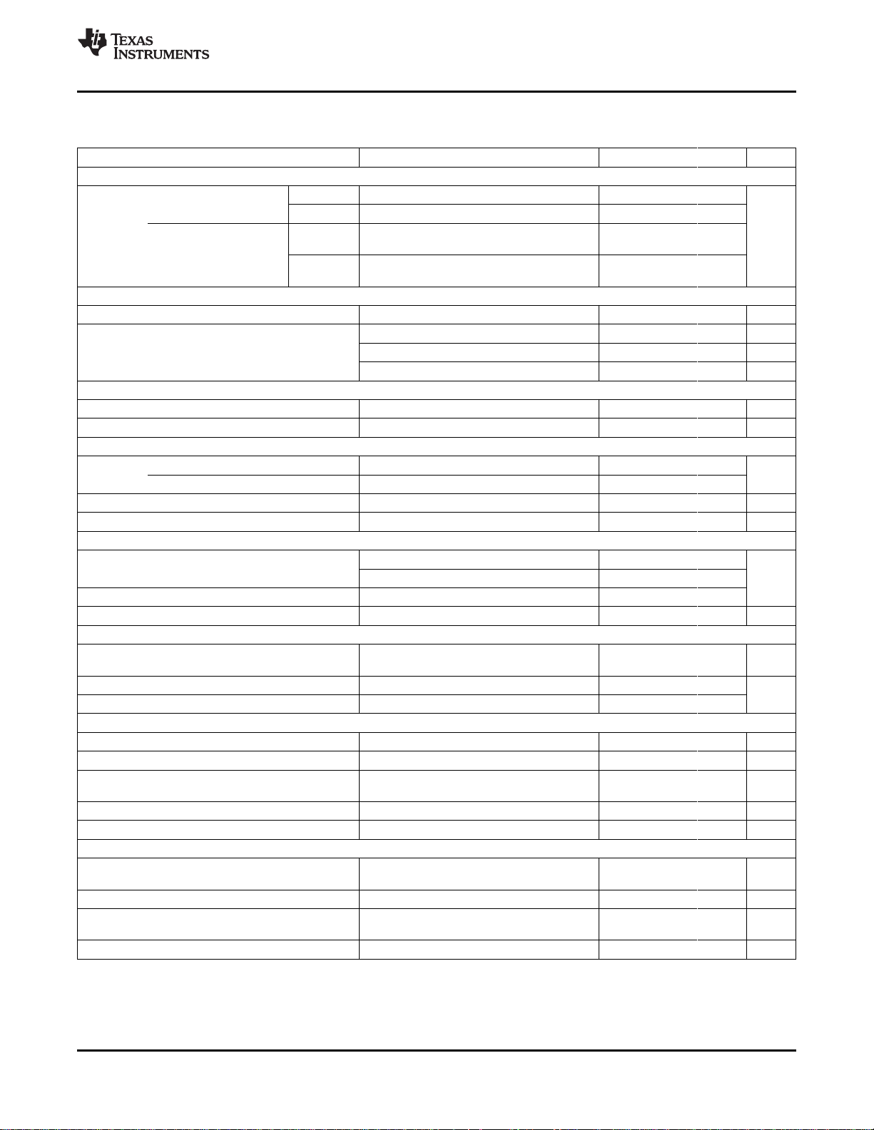
ELECTRICAL CHARACTERISTICS
TJ= – 40 ° C to 125 ° C, V
PARAMETER TEST CONDITIONS MIN TYP MAX UNIT
VOLTAGE REFERENCE
Feedback voltage range
V
FB
INPUT SUPPLY
V
VDD
I
VDD
UNDERVOLTAGE LOCKOUT
V
UVLO(on)
V
UVLO(hyst)
OSCILLATOR
f
OSC
V
SLP
PWM
t
ON(min)
t
OFF(min)
V
VLY
SOFT-START
V
SS(ofst)
R
SS(chg)
R
SS(dchg)
ERROR AMPLIFIER
GBWP Unity gain bandwidth product
A
OL
I
IB(FB)
I
COMP(src)
I
COMP(snk)
OVERCURRENT PROTECTION
V
ISNS(oc)
D
OC
V
SS(rst)
T
BLNK
(1) Ensured by design. Not production tested.
Input voltage range 4.5 52 V
Operating current 2.5 ≤ V
Turn on threshold voltage 4.00 4.25 4.50 V
UVLO hysteresis 140 195 240 mV
Oscillator frequency range
Oscillator frequency R
Frequency line regulation 4.5 ≤ V
Slope compensation ramp 520 620 720 mV
Minimum pulse width
Minimum off time 170 200
Valley voltage 1.2 V
Offset voltage from SS pin to error
amplifier input
Soft-start charge resistance 320 430 600
Soft-start discharge resistance 840 1200 1600
Open loop gain
Input bias current (current out of FB
pin)
Output source current V
Output sink current V
Overcurrent detection threshold (at
ISNS pin)
Overcurrent duty cycle
Overcurrent reset threshold voltage (at
SS pin)
Leading edge blanking
= 12 Vdc, all parameters at zero power dissipation (unless otherwise noted)
VDD
(1)
TPS40210 COMP = FB, 4.5 ≤ V
TPS40211 COMP=FB, 4.5 ≤ V
TPS40210 686 700 714
TPS40211 250 260 270
(1)
(1)
(1)
COMP = FB, 4.5 ≤ V
125 ° C
COMP = FB, 4.5 ≤ V
125 ° C
4.5 ≤ V
V
VDD
RC
V
VDD
V
VDD
FB
FB
4.5 ≤ V
≤ 52 V, no switching, V
VDD
≤ 7 V 10 20 µ A
DIS
< V
UVLO(on)
= 182 k Ω , C
≤ 52 V -20% 7%
DD
(1)
= 12V
= 30V 90 200 ns
= 0.6 V, V
= 1.2 V, V
COMP
COMP
< 52 V, -40 ° C ≤ TJ≤ 125 ° C 120 150 180 mV
DD
≤ 52 V, TJ= 25 ° C 693 700 707
VDD
≤ 52 V, TJ= 25 ° C 254 260 266
VDD
≤ 52 V, -40 ° C ≤ T
VDD
≤ 52 V, -40 ° C ≤ T
VDD
DIS
, V
< 0.8 530 µ A
DIS
= 330 pF 260 300 340
RC
≤
J
≤
J
< 0.8 1.5 2.5 mA
= 1 V 100 250 µ A
= 1 V 1.2 2.5 mA
100 150 350 mV
(1)
35 1000
275 400
700 mV
1.5 3.0 MHz
60 80 dB
100 300 nA
2%
75 ns
mV
kHz
k Ω
Copyright © 2008, Texas Instruments Incorporated Submit Documentation Feedback 3
Product Folder Link(s): TPS40210 TPS40211
TPS40210 , TPS40211
SLUS772B – MARCH 2008 – REVISED JUNE 2008 ..........................................................................................................................................................
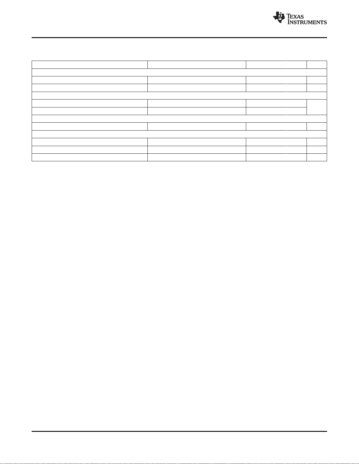
ELECTRICAL CHARACTERISTICS (continued)
TJ= – 40 ° C to 125 ° C, V
CURRENT SENSE AMPLIFIER
A
CS
I
B(ISNS)
DRIVER
I
GDRV(src)
I
GDRV(snk)
LINEAR REGULATOR
V
BP
DISABLE/ENABLE
V
DIS(en)
V
DIS(hys)
R
DIS
Current sense amplifier gain 4..2 5.6 7.2 V/V
Input bias current 1 3 µ A
Gate driver source current V
Gate driver sink current V
Bypass voltage output 0 mA < IBP< 15 mA 7 8 9 V
Turn on voltage 0.7 1.3 V
Hysteresis voltage 25 130 220 mV
DIS pin pulldown resistance 0.7 1.1 1.5 M Ω
PARAMETER TEST CONDITIONS MIN TYP MAX UNIT
= 12 Vdc, all parameters at zero power dissipation (unless otherwise noted)
VDD
= 4 V, TJ= 25 ° C 375 400
GDRV
= 4 V, TJ= 25 ° C 330 400
GDRV
www.ti.com
mA
4 Submit Documentation Feedback Copyright © 2008, Texas Instruments Incorporated
Product Folder Link(s): TPS40210 TPS40211
0
400
800
1200
100
200
600
100
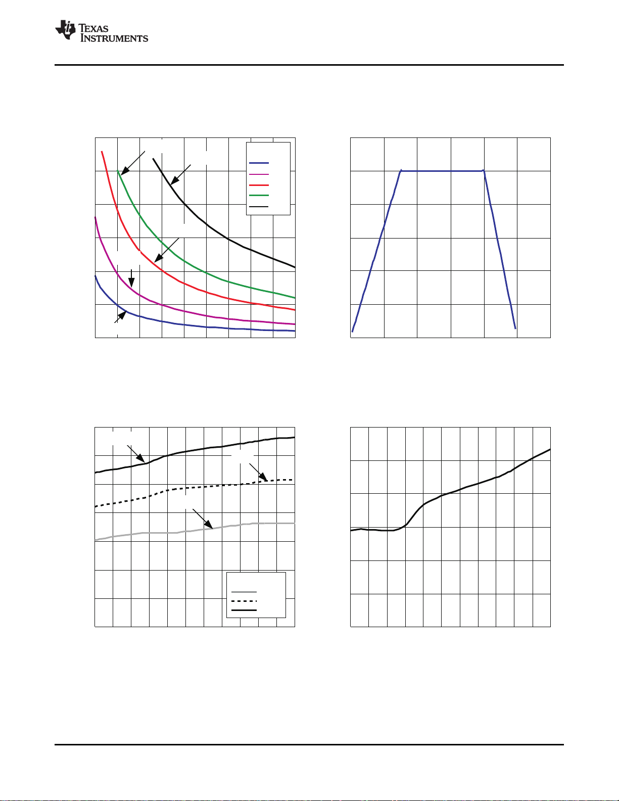
f
SW
- Frequency - kHz
RT- Timing Resistance - kW
300
CT(pF)
470
220
100
68
33
470 pF
220 pF
100pF
68 pF
33pF
200 400 600500 800 1000900700
0
400
800
1200
0
200
600
1000
f
SW
- Frequency - kHz
D - Duty Cycle
0.2 0.4 0.8 1.20.6
1.0
0
0.4
1.4
-40
0.2
1.2
I
VDD
– Quiescent Current – mA
TJ– Junction Temperature – ° C
-10-25 5 5020 80 1259565
35 110
0.8
0.6
1.0
52 V
4.5 V
12 V
12 V
4.5 V
52 V
V
VDD
0
6
-40
1
5
I
VDD
– Shutdown Current – mA
TJ– Junction Temperature – ° C
-10-25 5 5020 80 125956535 110
3
2
4
TPS40210 , TPS40211
www.ti.com
.......................................................................................................................................................... SLUS772B – MARCH 2008 – REVISED JUNE 2008
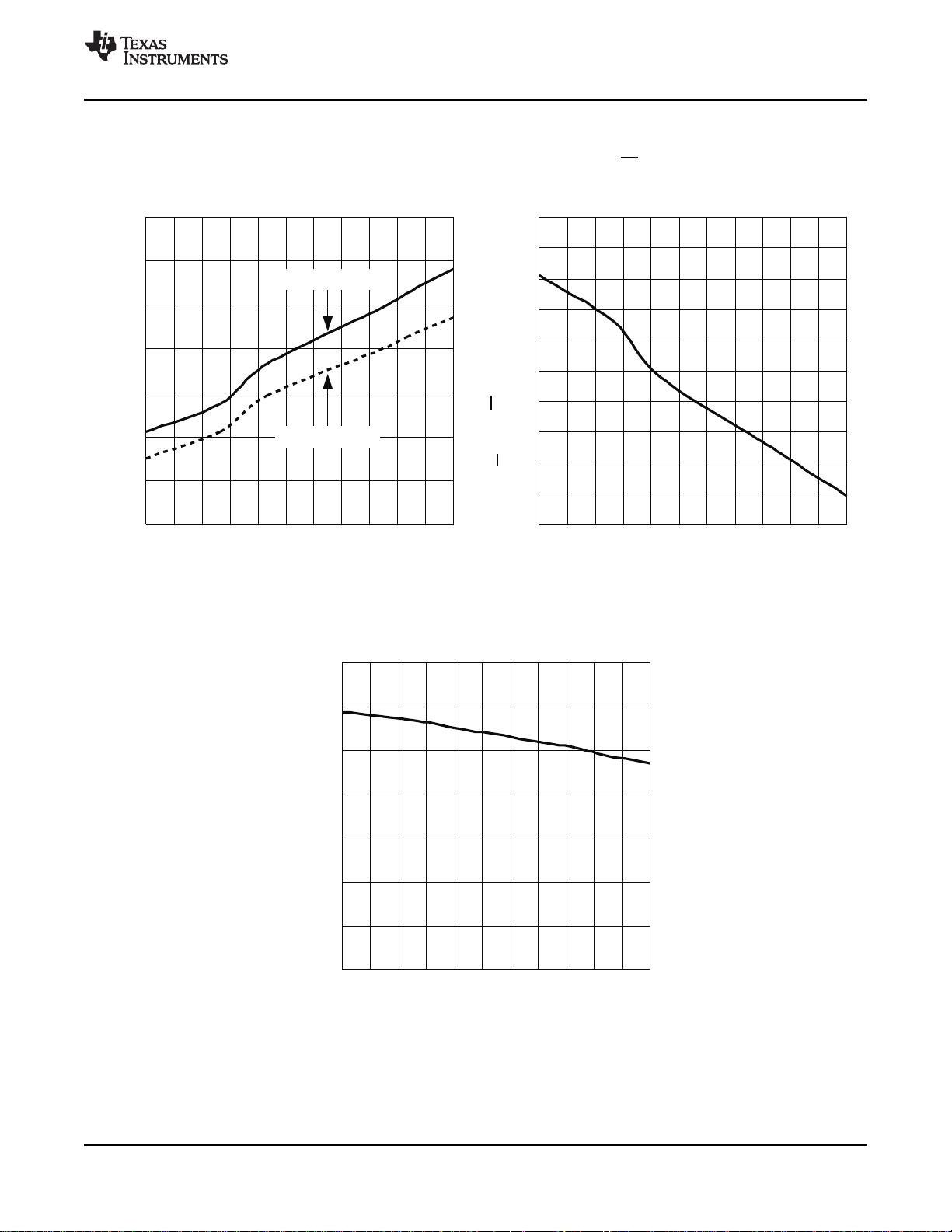
TYPICAL CHARACTERISTICS
FREQUENCY SWITCHING FREQUENCY
TIMING RESISTANCE DUTY CYCLE
vs vs
Figure 1. Figure 2.
QUIESCENT CURRENT SHUTDOWN CURRENT
JUNCTION TEMPERATURE JUNCTION TEMPERATURE
vs vs
Figure 3. Figure 4.
Copyright © 2008, Texas Instruments Incorporated Submit Documentation Feedback 5
Product Folder Link(s): TPS40210 TPS40211
-0.8
-0.4
0.4
-40
-0.6
0.2
V
FB
– Reference Voltage Change – %
TJ– Junction Temperature – ° C
-10-25 5 5020 80 125956535 110
0.0
-0.2
12 V
4.5 V
52 V
V
VDD
52 V
4.5 V
12 V
-0.5
-0.3
0.5
0
-0.4
0.4
V
FB
– Reference Voltage Change – %
V
VDD
– Input Voltage – V
10 3020 605040
0.1
0.0
0.2
-0.1
-0.2
0.3
4.00
4.30
-40
4.05
4.25
V
UVLO
– Undervoltage Lockout Threshold – V
TJ– Junction Temperature – ° C
-10-25 5 5020 80 125956535 110
4.15
4.10
4.20
UVLO On
UVLO Off
Off
On
UVLO
147
150
155
-40
148
154
V
ISNS(OC)
– Overcurrent Threshold – mV
TJ– Junction Temperature – ° C
-10-25 5 5020 80 125956535 110
152
151
4.5 V
7.5 V
30 V
12 V & 20 V
4.5 V
7.5 V
V
VDD
30 V
12 V & 20 V
153
149
TPS40210 , TPS40211
SLUS772B – MARCH 2008 – REVISED JUNE 2008 ..........................................................................................................................................................
www.ti.com
TYPICAL CHARACTERISTICS (continued)
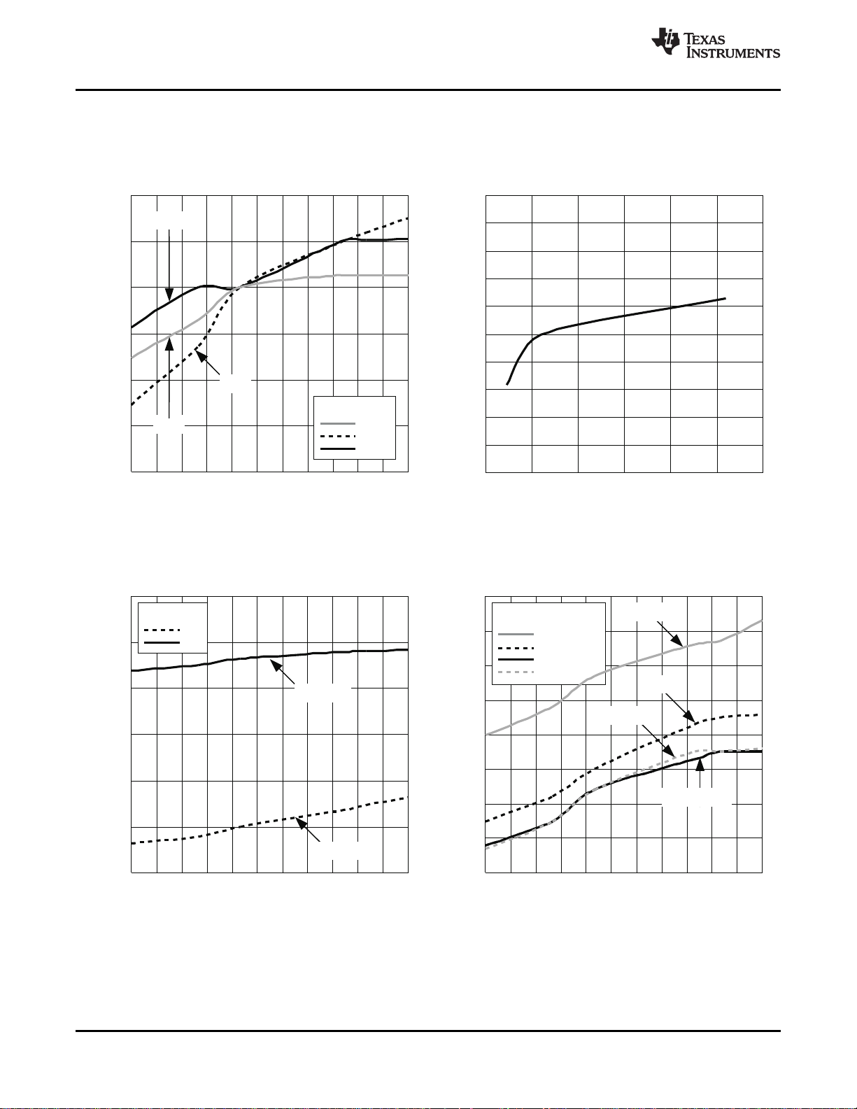
REFERENCE VOLTAGE CHANGE REFERENCE VOLTAGE CHANGE
JUNCTION TEMPERATURE INPUT VOLTAGE
vs vs
Figure 5. Figure 6.
UNDERVOLTAGE LOCKOUT THRESHOLD OVERCURRENT THRESHOLD
vs vs
JUNCTION TEMPERATURE JUNCTION TEMPERATURE
Figure 7. Figure 8.
6 Submit Documentation Feedback Copyright © 2008, Texas Instruments Incorporated
Product Folder Link(s): TPS40210 TPS40211
V
ISNS(OC)
– Overcurrent Threshold – mV
0
V
VDD
– Input Voltage – V
5 1510 452520
145
148
155
146
153
151
149
152
154
150
147
3530 40
-5
-2
5
-40
-4
3
f
OSC
– Switching Frequency Change – %
TJ– Junction Temperature – ° C
-10-25 5 5020 80 125956535 110
1
-1
2
4.5 V
12 V
30 V
30 V
12 V
4.5 V
4
0
-3
V
VDD
(V)
15
29
-40
17
27
Slope Compensation Ratio (V
VDD
/V
SLP
)
TJ– Junction Temperature – ° C
-10-25 5 5020 80 125956535 110
23
19
25
21
36 V
12 V
4.5 V
24 V
V
VDD
(V)
12 V
24 V
4.5 V
36 V
0
400
1400
-40
200
1200
R
SS
– Soft Start Charge/Discharge Resistance - kW
TJ– Junction Temperature – ° C
-10-25 5 5020 80 125956535 110
1000
800
R
SS(DSCH)
Discharge
R
SS(CHG)
Charge
600
TPS40210 , TPS40211
www.ti.com
.......................................................................................................................................................... SLUS772B – MARCH 2008 – REVISED JUNE 2008
TYPICAL CHARACTERISTICS (continued)
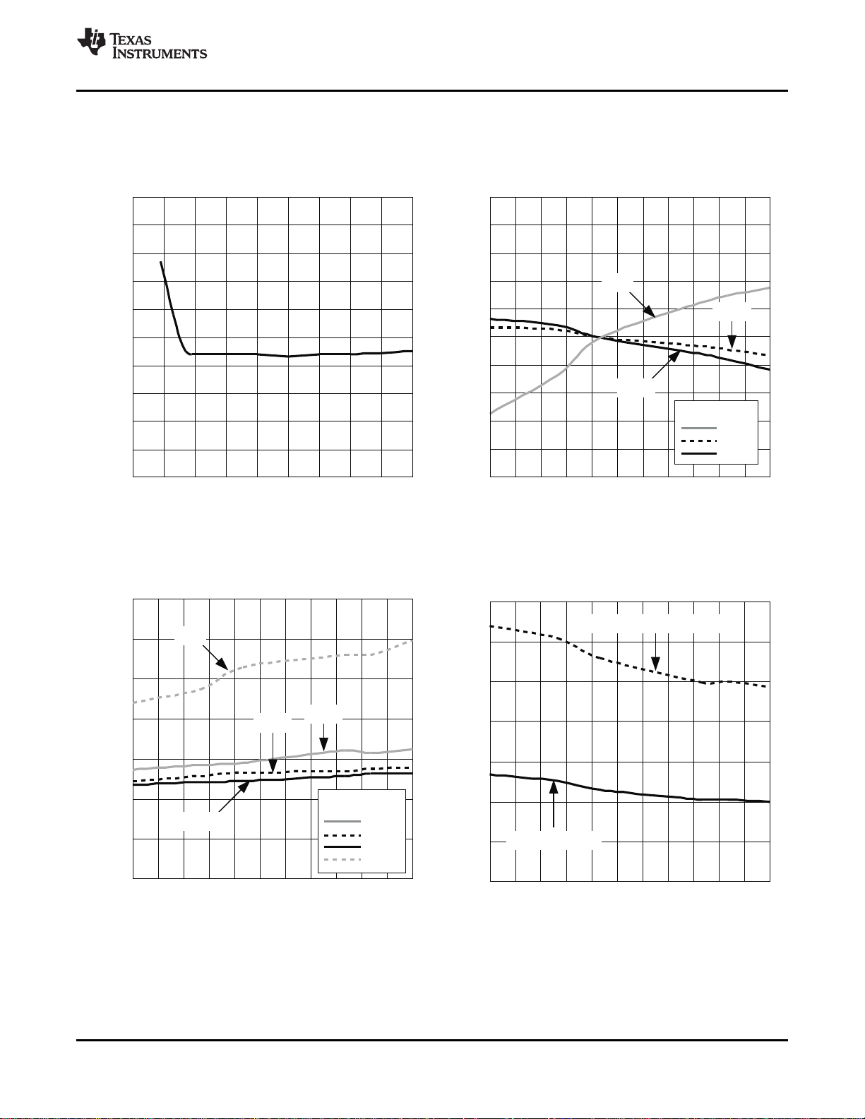
OVERCURRENT THRESHOLD SWITCHING FREQUENCY CHANGE
vs vs
INPUT VOLTAGE JUNCTION TEMPERATURE
Figure 9. Figure 10.
OSCILLATOR AMPLITUDE SOFT-START CHARGE/DISCHARGE RESISTANCE
vs vs
JUNCTION TEMPERATURE JUNCTION TEMPERATURE
Copyright © 2008, Texas Instruments Incorporated Submit Documentation Feedback 7
Figure 11. Figure 12.
Product Folder Link(s): TPS40210 TPS40211
0
40
180
-40
20
160
I
IB(FB)
– Feedback Bias Current – nA
TJ– Junction Temperature – ° C
-10-25 5 5020 80 125956535 110
100
80
120
60
140
0
100
300
-40
50
250
I
COMP(SRC)
– Compensation Source Current – mA
TJ– Junction Temperature – ° C
-10-25 5 5020 80 125956535 110
200
150
-40
I
COMP(SNK)
– Compensation Sink Current – mA
TJ– Junction Temperature – ° C
-10-25 5 5020 80 125956535 110
0
100
300
50
250
200
150
-40
V
VLY
– Valley Voltage Change – %
TJ– Junction Temperature – ° C
-10-25 5 5020 80 125956535 110
-5
-2
5
-4
3
1
-1
2
4
0
-3
TPS40210 , TPS40211
SLUS772B – MARCH 2008 – REVISED JUNE 2008 ..........................................................................................................................................................
www.ti.com
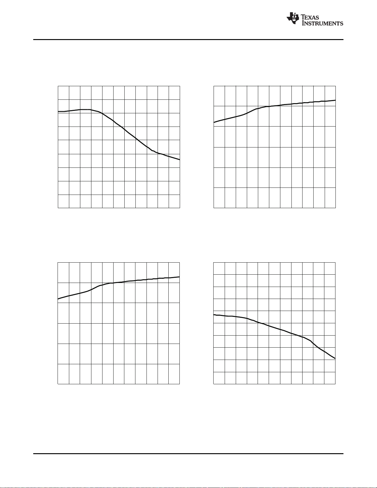
TYPICAL CHARACTERISTICS (continued)
FB BIAS CURRENT COMPENSATION SOURCE CURRENT
JUNCTION TEMPERATURE JUNCTION TEMPERATURE
vs vs
Figure 13. Figure 14.
COMPENSATION SINK CURRENT VALLEY VOLTAGE CHANGE
JUNCTION TEMPERATURE JUNCTION TEMPERATURE
vs vs
Figure 15. Figure 16.
8 Submit Documentation Feedback Copyright © 2008, Texas Instruments Incorporated
Product Folder Link(s): TPS40210 TPS40211
7.4
7.8
8.8
-40
7.6
8.6
V
BP
– Regulator Voltage – V
TJ– Junction Temperature – ° C
-10-25 5 5020 80 125956535 110
8.4
8.2
I
LOAD
= 0 mA
8.0
I
LOAD
= 5 mA
1.00
1.02
1.10
-40
1.01
1.09
V
DIS(EN)
– DIS/EN Turn-On Threshold – mV
TJ– Junction Temperature – ° C
-10-25 5 5020 80 125956535 110
1.06
1.05
1.07
1.03
1.08
1.06
A
CS
– Current Sense Amplifier Gain – V/V
0
2
7
4
3
5
6
1
-40
TJ– Junction Temperature – ° C
-10-25 5 5020 80 125956535 110
TPS40210 , TPS40211
www.ti.com
.......................................................................................................................................................... SLUS772B – MARCH 2008 – REVISED JUNE 2008
TYPICAL CHARACTERISTICS (continued)
REGULATOR VOLTAGE DIS/ EN TURN-ON THRESHOLD
JUNCTION TEMPERATURE JUNCTION TEMPERATURE
vs vs
Figure 17. Figure 18.
CURRENT SENSE AMPLIFIER GAIN
JUNCTION TEMPERATURE
vs
Figure 19.
Copyright © 2008, Texas Instruments Incorporated Submit Documentation Feedback 9
Product Folder Link(s): TPS40210 TPS40211
1
65
10
2
3
74
8
9
FB
RC
COMP
DIS/EN
SS
GND
VDD
ISNS
GDRV
BP
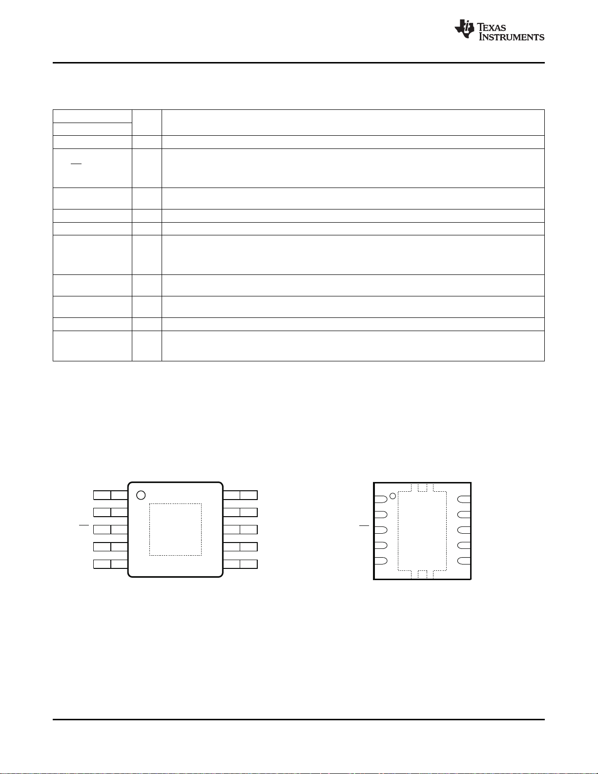
DGQ PowerPAD PACKAGE
(Top View)
FB
RC
COMP
DIS/EN
SS
5
4
3
2
1
1
6
7
8
9
10
GND
VDD
ISNS
GDRV
BP
DRC SURFACE MOUNT PACKAGE
(Top View)
TPS40210 , TPS40211
SLUS772B – MARCH 2008 – REVISED JUNE 2008 ..........................................................................................................................................................
DEVICE INFORMATION
TERMINAL FUNCTIONS
TERMINAL
NAME NO.
COMP 4 O Error amplifier output. Connect control loop compensation network between COMP pin and FB pin.
DIS/ EN 3 I
FB 5 I
GDRV 8 O Connect the gate of the power N channel MOSFET to this pin.
GND 6 - Device ground.
ISNS 7 I
RC 1 I
SS 2 I
BP 9 O Regulator output pin. Connect a 1.0- µ F bypass capacitor from this pin to GND.
VDD 10 I required slope compensation, this pin can be connected to the converter output. See Application Information
I/O DESCRIPTION
Disable pin. Pulling this pin high, places the part into a shutdown mode. Shutdown mode is characterized by
a very low quiescent current. While in shutdown mode, the functionality of all blocks is disabled and the BP
regulator is shut down. This pin has an internal 1-M Ω pull-down resistor to GND. Leaving this pin
unconnected enables the device.
Error amplifier inverting input. Connect a voltage divider from the output to this pin to set output voltage.
Compensation network is connected between this pin and COMP.
Current sense pin. Connect an external current sensing resistor between this pin and GND. The voltage on
this pin is used to provide current feedback in the control loop and detect an overcurrent condition. An
overcurrent condition is declared when ISNS pin voltage exceeds the overcurrent threshold voltage, 150 mV
typical.
Switching frequency setting pin. Connect capacitor from RC pin to GND. Connect a resistor from RC pin
toVDD of the IC power supply and a capacitor from RC to GND.
Soft-start time programming pin. Connect capacitor from SS pin to GND to program converter soft-start time.
This pin also functions as a timeout timer when the power supply is in an overcurrent condition.
System input voltage. Connect a local bypass capacitor from this pin to GND. Depending on the amount of
section for additional details.
www.ti.com
10 Submit Documentation Feedback Copyright © 2008, Texas Instruments Incorporated
DGQ PowerPAD PACKAGE DRC PACKAGE
(TOP VIEW) (TOP VIEW)
Product Folder Link(s): TPS40210 TPS40211
+
+
Soft Start
and
Overcurrent
5FB
4COMP
3DIS/EN
700 mV
LDO
PWM
Logic
2SS
1RC
Oscillator
and
Slope
Compensation
UVLO
Driver
9 BP
10 VDD
8 GDRV
6 GND
7 ISNS
+
Gain = 6
+
150 mV
LEB
OC Fault
OC Fault
UDG-07107
Enable E/A
E/A
SS Ref
TPS40210 , TPS40211
www.ti.com
.......................................................................................................................................................... SLUS772B – MARCH 2008 – REVISED JUNE 2008
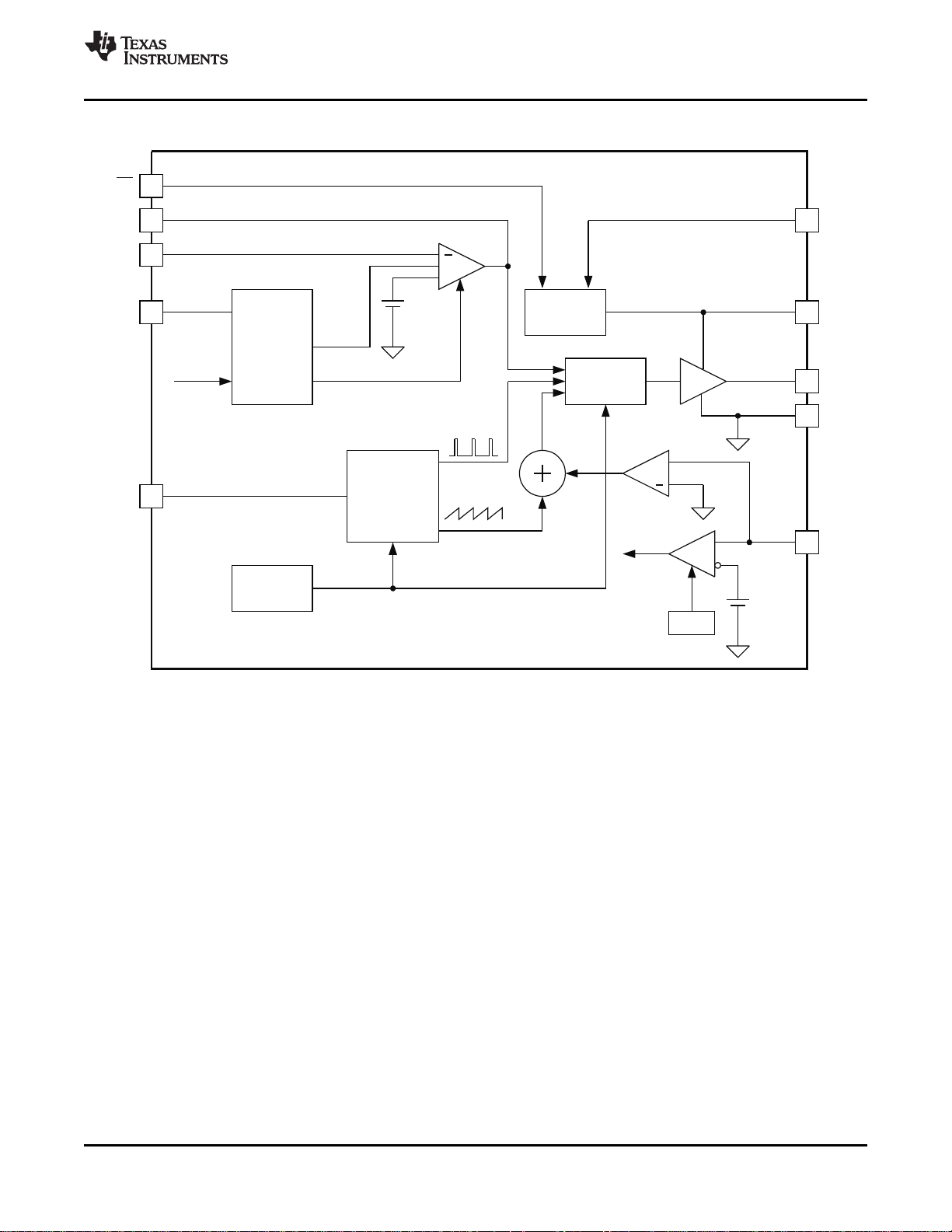
FUNCTIONAL BLOCK DIAGRAM
Copyright © 2008, Texas Instruments Incorporated Submit Documentation Feedback 11
Product Folder Link(s): TPS40210 TPS40211

OUT D
IN
V V
1
V 1 D
+
=
-
IN
OUT D
V
D 1
V V
æ ö
æ ö
= -
ç ÷
ç ÷
ç ÷
+
è ø
è ø
( )
( )
f
OUT D OUT SW
2
IN
2 V V I L
D
V
´ + ´ ´ ´
=
( )
( )
( )
f
2
OUT D IN IN
OUT(crit)
2
OUT D SW
V V V V
I
2 V V L
+ - ´
=
´ + ´ ´
TPS40210 , TPS40211
SLUS772B – MARCH 2008 – REVISED JUNE 2008 ..........................................................................................................................................................
www.ti.com
APPLICATION INFORMATION
Minimum On-Time and Off Time Considerations
The TPS40210 has a minimum off time of approximately 200 ns and a minimum on time of 300 ns. These two
constraints place limitations on the operating frequency that can be used for a given input to output conversion
ratio. See Figure 2 for the maximum frequency that can be used for a given duty cycle.
The duty cycle at which the converter operates is dependent on the mode in which the converter is running. If the
converter is running in discontinuous conduction mode, the duty cycle varies with changes to the load much
more than it does when running in continuous conduction mode.
In continuous conduction mode, the duty cycle is related primarily to the input and output voltages.
In discontinuous mode the duty cycle is a function of the load, input and output voltages, inductance and
switching frequency.
(1)
(2)
All converters using a diode as the freewheeling or catch component have a load current level at which they
transition from discontinuous conduction to continuous conduction. This is the point where the inductor current
just falls to zero. At higher load currents, the inductor current does not fall to zero but remains flowing in a
positive direction and assumes a trapezoidal wave shape as opposed to a triangular wave shape. This load
boundary between discontinuous conduction and continuous conduction can be found for a set of converter
parameters as follows.
For loads higher than the result of Equation 4 , the duty cycle is given by Equation 2 and for loads less that the
results of Equation 4 , the duty cycle is given Equation 3 . For Equations 1 through 4, the variable definitions are
as follows.
• V
• V
• V
• I
is the output voltage of the converter in V
OUT
is the forward conduction voltage drop across the rectifier or catch diode in V
D
is the input voltage to the converter in V
IN
is the output current of the converter in A
OUT
• L is the inductor value in H
• fSWis the switching frequency in Hz
(3)
(4)
12 Submit Documentation Feedback Copyright © 2008, Texas Instruments Incorporated
Product Folder Link(s): TPS40210 TPS40211
T
8 10 2 7 4 6 9 2
SW T SW SW T T
1
R
5.8 10 f C 8 10 f 1.4 1 0 f 1.5 10 1.7 10 C 4 10 C
- - - - - -
=
´ ´ ´ + ´ ´ + ´ ´ - ´ + ´ ´ - ´ ´
+
1
RC
150 mV
S Q
QR
+
+
8
5
VDD
GND
R
RC
C
RC
CLK
External Frequency
Synchronization
(optional)
V
IN
TPS40210/11
UDG-08063
TPS40210 , TPS40211
www.ti.com
.......................................................................................................................................................... SLUS772B – MARCH 2008 – REVISED JUNE 2008
Setting the Oscillator Frequency
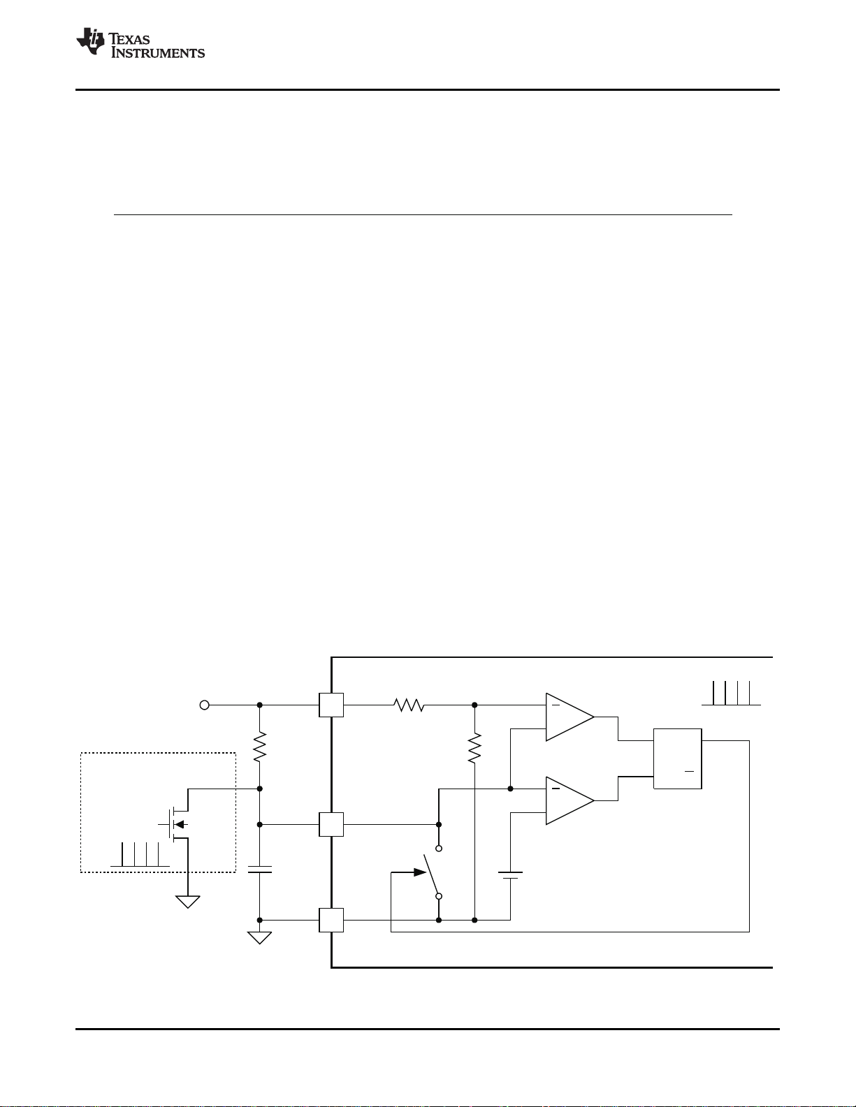
The oscillator frequency is determined by a resistor and capacitor connected to the RC pin of the TPS40210. The
capacitor is charged to a level of approximately V
/20 by current flowing through the resistor and is then
VDD
discharged by a transistor internal to the TPS40210. The required resistor for a given oscillator frequency is
found from either Figure 1 or Equation 5 .
where
• RTis the timing resistance in k Ω
• fSWis the switching frequency in kHz
• CTis the timing capacitance in pF
For most applications a capacitor in the range of 68 pF to 120 pF gives the best results. Resistor values should
be limited to between 100 k Ω and 1 M Ω as well. If the resistor value falls below 100 k Ω , decrease the capacitor
size and recalculate the resistor value for the desired frequency. As the capacitor size decreases below 47 pF,
the accuracy of Equation 5 degrades and empirical means may be needed to fine tune the timing component
values to achieve the desired switching frequency.
Synchronizing the Oscillator
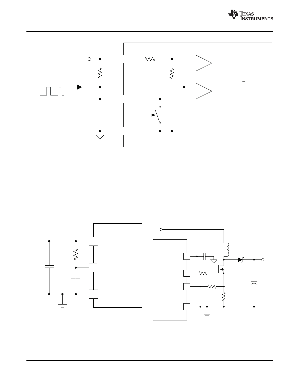
The TPS40210 and TPS40211 can be synchronized to an external clock source. Figure 20 shows the functional
diagram of the oscillator. When synchronizing the oscillator to an external clock, the RC pin must be pulled below
150 mV for 20 ns or more. The external clock frequency must be higher than the free running frequency of the
converter as well. When synchronizing the controller, if the RC pin is held low for an excessive amount of time,
erratic operation may occur. The maximum amount of time that the RC pin should be held low is 50% of a
nominal output pulse, or 10% of the period of the synchronization frequency.
Under circumstances where the duty cycle is less than 50%, a Schottky diode connected from the RC pin to an
external clock may be used to synchronize the oscillator. The cathode of the diode is connected to the RC pin.
The trip point of the oscillator is set by an internal voltage divider to be 1/20 of the input voltage. The clock signal
must have an amplitude higher than this trip point. When the clock goes low, it allows the reset current to restart
the RC ramp, synchronizing the oscillator to the external clock. This provides a simple, single-component method
for clock synchronization.
(5)
Copyright © 2008, Texas Instruments Incorporated Submit Documentation Feedback 13
Figure 20. Oscillator Functional Diagram
Product Folder Link(s): TPS40210 TPS40211
+
1
RC
TPS40210/11
150 mV
S Q
QR
+
+
8
5
VDD
GND
R
RC
C
RC
CLK
Frequency > Controller
Frequency
V
IN
Amplitude >
20
V
IN
Duty Cycle < 50%
UDG-08064
10
1
6
TPS40210/11
VDD
RC
GND
C
T
R
T
UDG-07119
10
8
7
VDD
ISNS
GDRV
GND
TPS40210/11
L
V
OUT
V
IN
6
R
ISNS
UDG-07120
C
IFLT
R
IFLT
TPS40210 , TPS40211
SLUS772B – MARCH 2008 – REVISED JUNE 2008 ..........................................................................................................................................................
www.ti.com
Figure 21. Diode Connected Synchronization
Current Sense and Overcurrent
The tps40210 and TPS40211 are current mode controllers and use a resistor in series with the source terminal
power FET to sense current for both the current mode control and overcurrent protection. The device enters a
current limit state if the voltage on the ISNS pin exceeds the current limit threshold voltage V
electrical specifications table. When this happens the controller discharges the SS capacitor through a relatively
high impedance and then attempt to restart. The amount of output current that causes this to happen is
dependent on several variables in the converter.
The load current overcurrent threshold is set by proper choice of R
discontinuous mode the current sense resistor is found in Equation 6 .
14 Submit Documentation Feedback Copyright © 2008, Texas Instruments Incorporated
Product Folder Link(s): TPS40210 TPS40211
Figure 22. Oscillator Components Figure 23. Current Sense Components
ISNS(oc)
. If the converter is operating in
ISNS
from the
 Loading...