

1
2
3
4
10
9
8
7
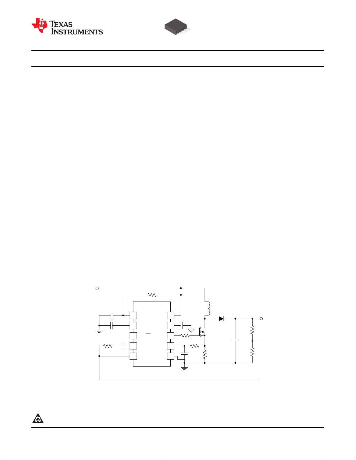
RC
DIS/EN
COMP
SS
VDD
ISNS
GDRV
GND
TPS40210
V
OUT
V
IN
5 FB 6
BP
R
SENSE
UDG-07110
TPS40210 , TPS40211
www.ti.com
.......................................................................................................................................................... SLUS772B – MARCH 2008 – REVISED JUNE 2008
4.5-V TO 52-V INPUT CURRENT MODE BOOST CONTROLLER
1
FEATURES CONTENTS
• For Boost, Flyback, SEPIC, LED Drive Apps
• Wide Input Operating Voltage: 4.5 V to 52 V
• Adjustable Oscillator Frequency
• Fixed Frequency Current Mode Control
• Internal Slope Compensation
• Integrated Low-Side Driver
• Programmable Closed Loop Soft Start
• Overcurrent Protection
• External Synchronization Capable
• Reference700-mV (TPS40210), 260-mV
(TPS40211)
• Low Current Disable Function
APPLICATIONS
• LED Lighting
• Industrial Control Systems
• Battery Powered Systems
Device Ratings 2
Electrical Characteristics 3
Typical Characteristics 5
Terminal Information 10
Application Information 12
Additional References 25
Design Examples 26
DESCRIPTION
The TPS40210 and TPS40211 are wide-input voltage
(4.5 V to 52 V), non-synchronous boost controllers.
They are suitable for topologies which require a
grounded source N-channel FET including boost,
flyback, SEPIC and various LED Driver applications.
The device features include programmable soft start,
overcurrent protection with automatic retry and
programmable oscillator frequency. Current mode
control provides improved transient response and
simplified loop compensation. The main difference
between the two parts is the reference voltage to
which the error amplifier regulates the FB pin.
1
Please be aware that an important notice concerning availability, standard warranty, and use in critical applications of Texas
Instruments semiconductor products and disclaimers thereto appears at the end of this data sheet.
PRODUCTION DATA information is current as of publication date.
Products conform to specifications per the terms of the Texas
Instruments standard warranty. Production processing does not
necessarily include testing of all parameters.
Copyright © 2008, Texas Instruments Incorporated
TPS40210 , TPS40211
SLUS772B – MARCH 2008 – REVISED JUNE 2008 ..........................................................................................................................................................
These devices have limited built-in ESD protection. The leads should be shorted together or the device placed in conductive foam
during storage or handling to prevent electrostatic damage to the MOS gates.
ORDERING INFORMATION
T
J
-40 ° C to 125 ° C
-40 ° C to 125 ° C
PACKAGE PART NUMBER
10-Pin MSOP
PowerPAD
10-Pin SON DRC
10-Pin MSOP
PowerPAD
10-Pin SON DRC
PACKAGE TAPE AND REEL
LEAD QUANTITY
DGQ
DGQ
2500 TPS40210DGQR
80 TPS40210DGQ
3000 TPS40210DRCR
250 TPS40210DRCT
2500 TPS40211DGQR
80 TPS40211DGQ
3000 TPS40211DRCR
250 TPS40211DRCT
DEVICE RATINGS
ABSOLUTE MAXIMUM RATINGS
over operating free-air temperature range unless otherwise noted
VDD – 0.3 to 52
Input voltage range RC, SS, FB, DIS/ EN – 0.3 to 10
ISNS – 0.3 to 8
Output voltage range COMP, BP, GDRV – 0.3 to 9
T
T
(1) Stresses beyond those listed under " absolute maximum ratings " may cause permanent damage to the device. These are stress ratings
Operating junction temperature range – 40 to 150
J
Storage temperature – 55 to 150
stg
only, and functional operation of the device at these or any other conditions beyond those indicated under " recommended operating
conditions " is not implied. Exposure to absolute-maximum-rated conditions for extended periods may affect device reliability.
(1)
TPS40210
TPS40211
www.ti.com
UNIT
V
° C
RECOMMENDED OPERATING CONDITIONS
MIN NOM MAX UNIT
V
T
Input voltage 4.5 52 V
VDD
Operating Junction temperature -40 125 ° C
J
PACKAGE DISSIPATION RATINGS
R
High-K Board
PACKAGE AIRFLOW (LFM)
10-Pin MSOP PowerPAD 0 (Natural Convection) 57.7 1.73 0.693
(DGQ)
10-Pin SON (DRC) 0 (Natural Convection) 47.9 2.08 0.835
(1) Ratings based on JEDEC High Thermal Conductivity (High K) Board. For more information on the test method, see TI Technical Brief
SZZA017.
θ JA
( ° C/W) TA= 25 ° C TA= 85 ° C
(1)
Power Rating (W) Power Rating (W)
ELECTROSTATIC DISCHARGE (ESD) PROTECTION
MIN TYP MAX UNIT
Human Body Model (HBM) 1500
Charged Device Model (CDM) 1500
2 Submit Documentation Feedback Copyright © 2008, Texas Instruments Incorporated
Product Folder Link(s): TPS40210 TPS40211
V
TPS40210 , TPS40211
www.ti.com
.......................................................................................................................................................... SLUS772B – MARCH 2008 – REVISED JUNE 2008
ELECTRICAL CHARACTERISTICS
TJ= – 40 ° C to 125 ° C, V
PARAMETER TEST CONDITIONS MIN TYP MAX UNIT
VOLTAGE REFERENCE
Feedback voltage range
V
FB
INPUT SUPPLY
V
VDD
I
VDD
UNDERVOLTAGE LOCKOUT
V
UVLO(on)
V
UVLO(hyst)
OSCILLATOR
f
OSC
V
SLP
PWM
t
ON(min)
t
OFF(min)
V
VLY
SOFT-START
V
SS(ofst)
R
SS(chg)
R
SS(dchg)
ERROR AMPLIFIER
GBWP Unity gain bandwidth product
A
OL
I
IB(FB)
I
COMP(src)
I
COMP(snk)
OVERCURRENT PROTECTION
V
ISNS(oc)
D
OC
V
SS(rst)
T
BLNK
(1) Ensured by design. Not production tested.
Input voltage range 4.5 52 V
Operating current 2.5 ≤ V
Turn on threshold voltage 4.00 4.25 4.50 V
UVLO hysteresis 140 195 240 mV
Oscillator frequency range
Oscillator frequency R
Frequency line regulation 4.5 ≤ V
Slope compensation ramp 520 620 720 mV
Minimum pulse width
Minimum off time 170 200
Valley voltage 1.2 V
Offset voltage from SS pin to error
amplifier input
Soft-start charge resistance 320 430 600
Soft-start discharge resistance 840 1200 1600
Open loop gain
Input bias current (current out of FB
pin)
Output source current V
Output sink current V
Overcurrent detection threshold (at
ISNS pin)
Overcurrent duty cycle
Overcurrent reset threshold voltage (at
SS pin)
Leading edge blanking
= 12 Vdc, all parameters at zero power dissipation (unless otherwise noted)
VDD
(1)
TPS40210 COMP = FB, 4.5 ≤ V
TPS40211 COMP=FB, 4.5 ≤ V
TPS40210 686 700 714
TPS40211 250 260 270
(1)
(1)
(1)
COMP = FB, 4.5 ≤ V
125 ° C
COMP = FB, 4.5 ≤ V
125 ° C
4.5 ≤ V
V
VDD
RC
V
VDD
V
VDD
FB
FB
4.5 ≤ V
≤ 52 V, no switching, V
VDD
≤ 7 V 10 20 µ A
DIS
< V
UVLO(on)
= 182 k Ω , C
≤ 52 V -20% 7%
DD
(1)
= 12V
= 30V 90 200 ns
= 0.6 V, V
= 1.2 V, V
COMP
COMP
< 52 V, -40 ° C ≤ TJ≤ 125 ° C 120 150 180 mV
DD
≤ 52 V, TJ= 25 ° C 693 700 707
VDD
≤ 52 V, TJ= 25 ° C 254 260 266
VDD
≤ 52 V, -40 ° C ≤ T
VDD
≤ 52 V, -40 ° C ≤ T
VDD
DIS
, V
< 0.8 530 µ A
DIS
= 330 pF 260 300 340
RC
≤
J
≤
J
< 0.8 1.5 2.5 mA
= 1 V 100 250 µ A
= 1 V 1.2 2.5 mA
100 150 350 mV
(1)
35 1000
275 400
700 mV
1.5 3.0 MHz
60 80 dB
100 300 nA
2%
75 ns
mV
kHz
k Ω
Copyright © 2008, Texas Instruments Incorporated Submit Documentation Feedback 3
Product Folder Link(s): TPS40210 TPS40211
TPS40210 , TPS40211
SLUS772B – MARCH 2008 – REVISED JUNE 2008 ..........................................................................................................................................................
ELECTRICAL CHARACTERISTICS (continued)
TJ= – 40 ° C to 125 ° C, V
CURRENT SENSE AMPLIFIER
A
CS
I
B(ISNS)
DRIVER
I
GDRV(src)
I
GDRV(snk)
LINEAR REGULATOR
V
BP
DISABLE/ENABLE
V
DIS(en)
V
DIS(hys)
R
DIS
Current sense amplifier gain 4..2 5.6 7.2 V/V
Input bias current 1 3 µ A
Gate driver source current V
Gate driver sink current V
Bypass voltage output 0 mA < IBP< 15 mA 7 8 9 V
Turn on voltage 0.7 1.3 V
Hysteresis voltage 25 130 220 mV
DIS pin pulldown resistance 0.7 1.1 1.5 M Ω
PARAMETER TEST CONDITIONS MIN TYP MAX UNIT
= 12 Vdc, all parameters at zero power dissipation (unless otherwise noted)
VDD
= 4 V, TJ= 25 ° C 375 400
GDRV
= 4 V, TJ= 25 ° C 330 400
GDRV
www.ti.com
mA
4 Submit Documentation Feedback Copyright © 2008, Texas Instruments Incorporated
Product Folder Link(s): TPS40210 TPS40211
0
400
800
1200
100
200
600
100
f
SW
- Frequency - kHz
RT- Timing Resistance - kW
300
CT(pF)
470
220
100
68
33
470 pF
220 pF
100pF
68 pF
33pF
200 400 600500 800 1000900700
0
400
800
1200
0
200
600
1000
f
SW
- Frequency - kHz
D - Duty Cycle
0.2 0.4 0.8 1.20.6
1.0
0
0.4
1.4
-40
0.2
1.2
I
VDD
– Quiescent Current – mA
TJ– Junction Temperature – ° C
-10-25 5 5020 80 1259565
35 110
0.8
0.6
1.0
52 V
4.5 V
12 V
12 V
4.5 V
52 V
V
VDD
0
6
-40
1
5
I
VDD
– Shutdown Current – mA
TJ– Junction Temperature – ° C
-10-25 5 5020 80 125956535 110
3
2
4
TPS40210 , TPS40211
www.ti.com
.......................................................................................................................................................... SLUS772B – MARCH 2008 – REVISED JUNE 2008
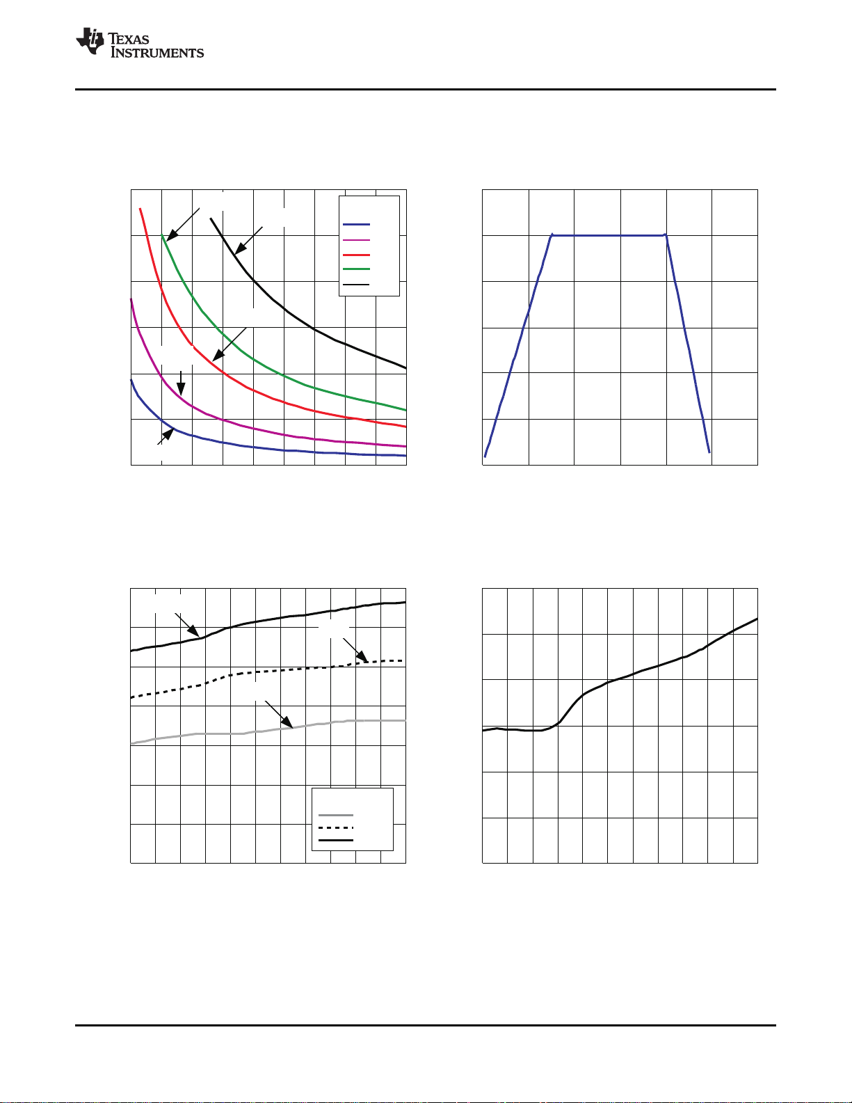
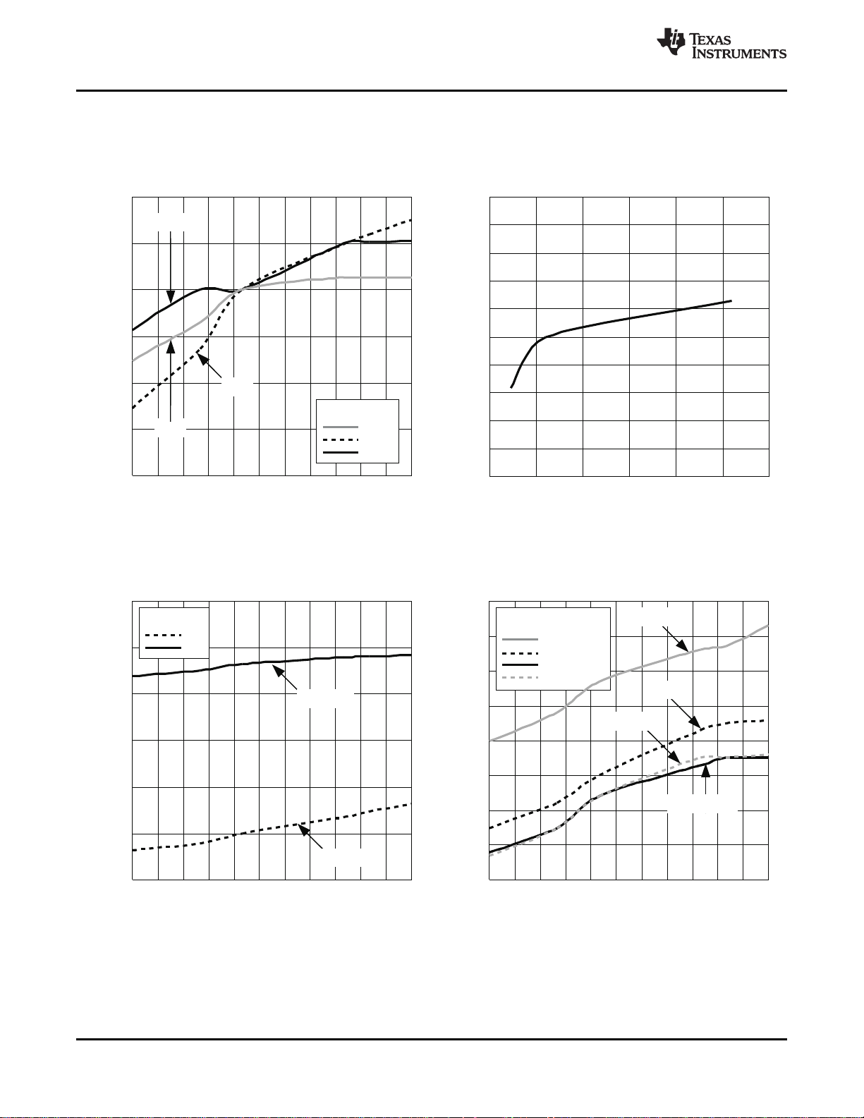
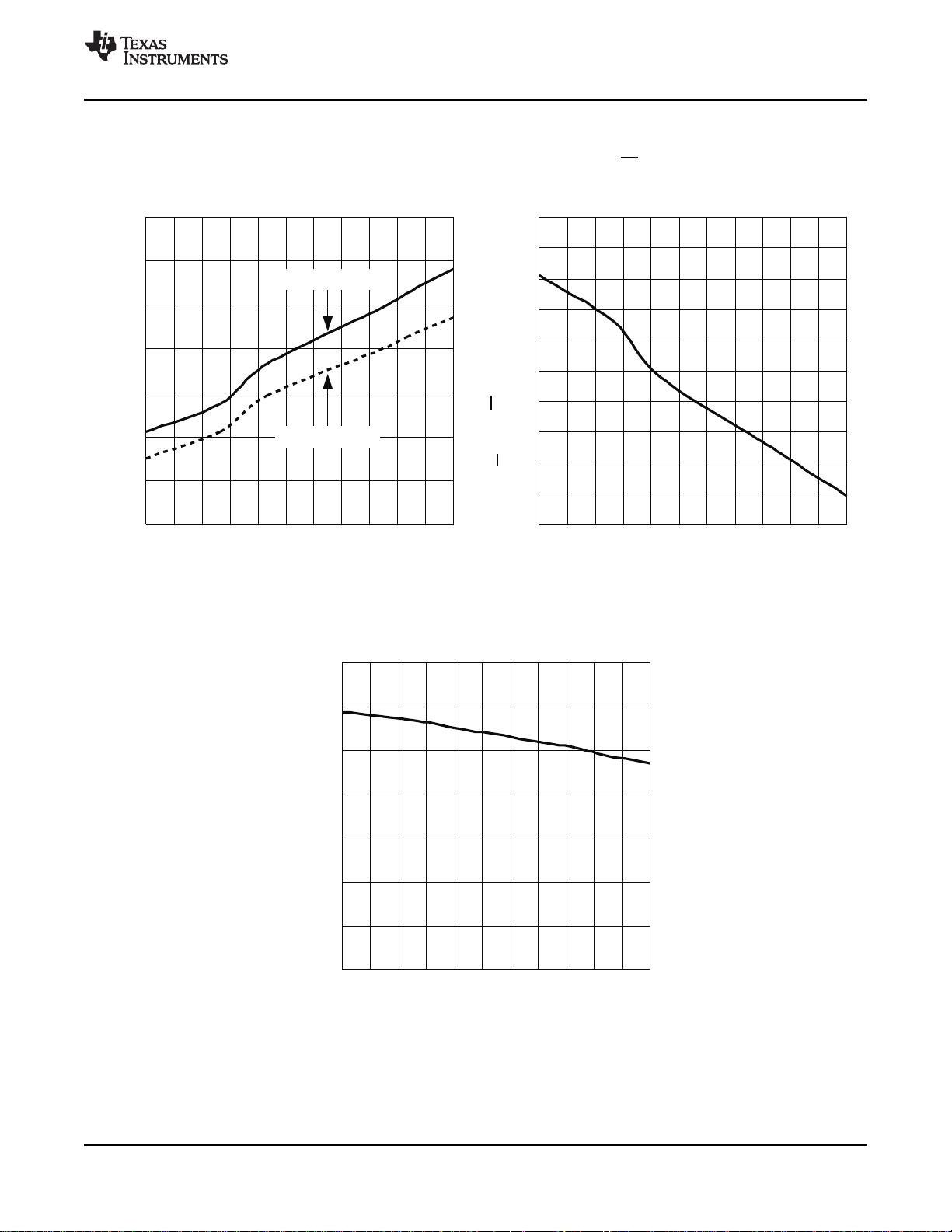
TYPICAL CHARACTERISTICS
FREQUENCY SWITCHING FREQUENCY
TIMING RESISTANCE DUTY CYCLE
vs vs
Figure 1. Figure 2.
QUIESCENT CURRENT SHUTDOWN CURRENT
JUNCTION TEMPERATURE JUNCTION TEMPERATURE
vs vs
Figure 3. Figure 4.
Copyright © 2008, Texas Instruments Incorporated Submit Documentation Feedback 5
Product Folder Link(s): TPS40210 TPS40211
-0.8
-0.4
0.4
-40
-0.6
0.2
V
FB
– Reference Voltage Change – %
TJ– Junction Temperature – ° C
-10-25 5 5020 80 125956535 110
0.0
-0.2
12 V
4.5 V
52 V
V
VDD
52 V
4.5 V
12 V
-0.5
-0.3
0.5
0
-0.4
0.4
V
FB
– Reference Voltage Change – %
V
VDD
– Input Voltage – V
10 3020 605040
0.1
0.0
0.2
-0.1
-0.2
0.3
4.00
4.30
-40
4.05
4.25
V
UVLO
– Undervoltage Lockout Threshold – V
TJ– Junction Temperature – ° C
-10-25 5 5020 80 125956535 110
4.15
4.10
4.20
UVLO On
UVLO Off
Off
On
UVLO
147
150
155
-40
148
154
V
ISNS(OC)
– Overcurrent Threshold – mV
TJ– Junction Temperature – ° C
-10-25 5 5020 80 125956535 110
152
151
4.5 V
7.5 V
30 V
12 V & 20 V
4.5 V
7.5 V
V
VDD
30 V
12 V & 20 V
153
149
TPS40210 , TPS40211
SLUS772B – MARCH 2008 – REVISED JUNE 2008 ..........................................................................................................................................................
www.ti.com
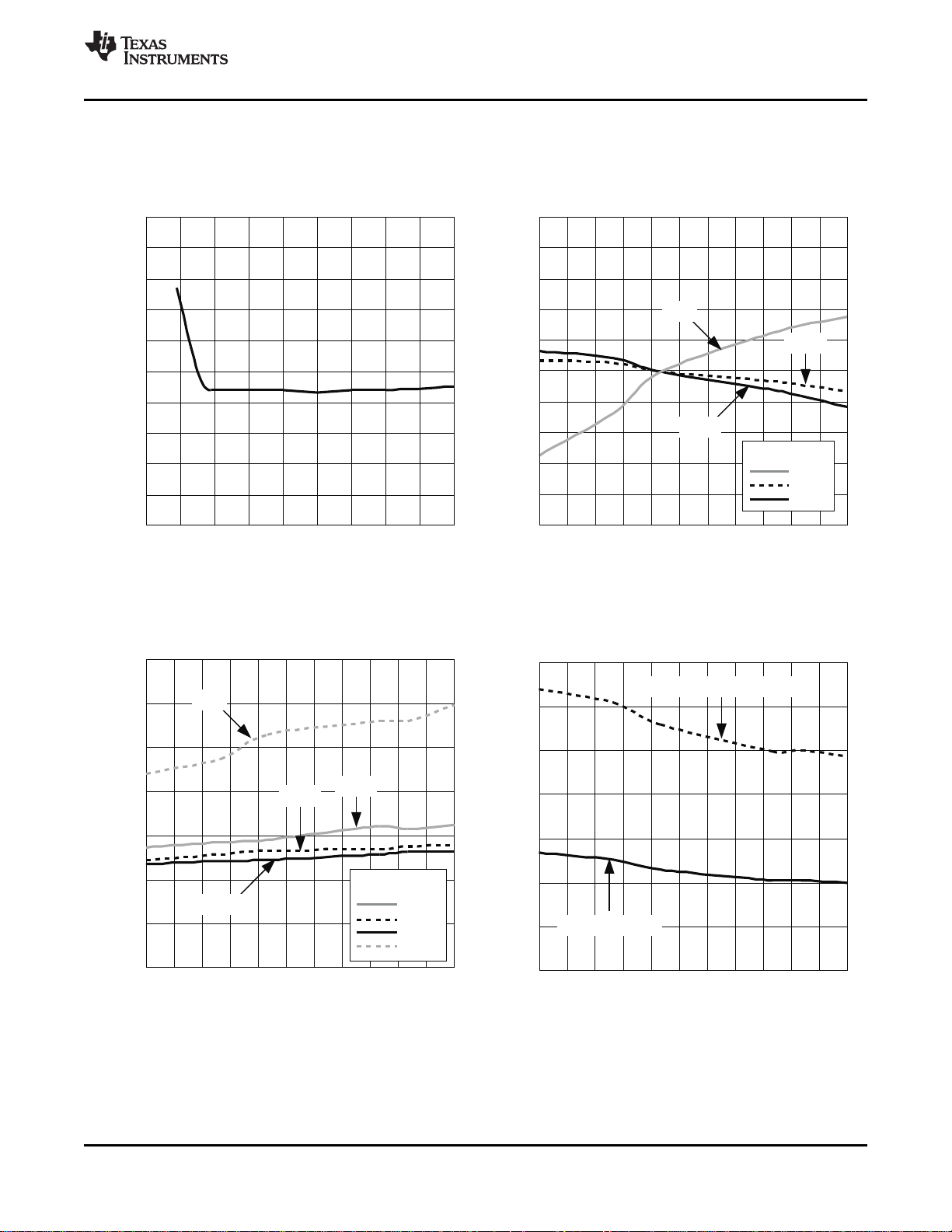
TYPICAL CHARACTERISTICS (continued)
REFERENCE VOLTAGE CHANGE REFERENCE VOLTAGE CHANGE
JUNCTION TEMPERATURE INPUT VOLTAGE
vs vs
Figure 5. Figure 6.
UNDERVOLTAGE LOCKOUT THRESHOLD OVERCURRENT THRESHOLD
vs vs
JUNCTION TEMPERATURE JUNCTION TEMPERATURE
Figure 7. Figure 8.
6 Submit Documentation Feedback Copyright © 2008, Texas Instruments Incorporated
Product Folder Link(s): TPS40210 TPS40211
V
ISNS(OC)
– Overcurrent Threshold – mV
0
V
VDD
– Input Voltage – V
5 1510 452520
145
148
155
146
153
151
149
152
154
150
147
3530 40
-5
-2
5
-40
-4
3
f
OSC
– Switching Frequency Change – %
TJ– Junction Temperature – ° C
-10-25 5 5020 80 125956535 110
1
-1
2
4.5 V
12 V
30 V
30 V
12 V
4.5 V
4
0
-3
V
VDD
(V)
15
29
-40
17
27
Slope Compensation Ratio (V
VDD
/V
SLP
)
TJ– Junction Temperature – ° C
-10-25 5 5020 80 125956535 110
23
19
25
21
36 V
12 V
4.5 V
24 V
V
VDD
(V)
12 V
24 V
4.5 V
36 V
0
400
1400
-40
200
1200
R
SS
– Soft Start Charge/Discharge Resistance - kW
TJ– Junction Temperature – ° C
-10-25 5 5020 80 125956535 110
1000
800
R
SS(DSCH)
Discharge
R
SS(CHG)
Charge
600
TPS40210 , TPS40211
www.ti.com
.......................................................................................................................................................... SLUS772B – MARCH 2008 – REVISED JUNE 2008
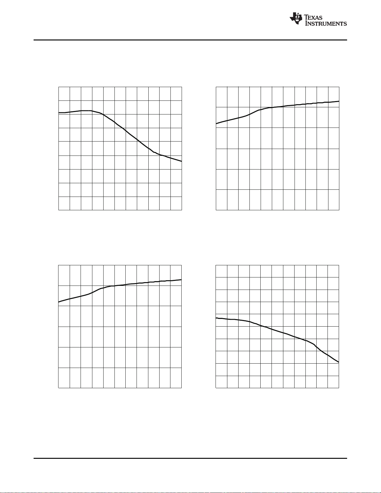
TYPICAL CHARACTERISTICS (continued)
OVERCURRENT THRESHOLD SWITCHING FREQUENCY CHANGE
vs vs
INPUT VOLTAGE JUNCTION TEMPERATURE
Figure 9. Figure 10.
OSCILLATOR AMPLITUDE SOFT-START CHARGE/DISCHARGE RESISTANCE
vs vs
JUNCTION TEMPERATURE JUNCTION TEMPERATURE
Copyright © 2008, Texas Instruments Incorporated Submit Documentation Feedback 7
Figure 11. Figure 12.
Product Folder Link(s): TPS40210 TPS40211
0
40
180
-40
20
160
I
IB(FB)
– Feedback Bias Current – nA
TJ– Junction Temperature – ° C
-10-25 5 5020 80 125956535 110
100
80
120
60
140
0
100
300
-40
50
250
I
COMP(SRC)
– Compensation Source Current – mA
TJ– Junction Temperature – ° C
-10-25 5 5020 80 125956535 110
200
150
-40
I
COMP(SNK)
– Compensation Sink Current – mA
TJ– Junction Temperature – ° C
-10-25 5 5020 80 125956535 110
0
100
300
50
250
200
150
-40
V
VLY
– Valley Voltage Change – %
TJ– Junction Temperature – ° C
-10-25 5 5020 80 125956535 110
-5
-2
5
-4
3
1
-1
2
4
0
-3
TPS40210 , TPS40211
SLUS772B – MARCH 2008 – REVISED JUNE 2008 ..........................................................................................................................................................
www.ti.com
TYPICAL CHARACTERISTICS (continued)
FB BIAS CURRENT COMPENSATION SOURCE CURRENT
JUNCTION TEMPERATURE JUNCTION TEMPERATURE
vs vs
Figure 13. Figure 14.
COMPENSATION SINK CURRENT VALLEY VOLTAGE CHANGE
JUNCTION TEMPERATURE JUNCTION TEMPERATURE
vs vs
Figure 15. Figure 16.
8 Submit Documentation Feedback Copyright © 2008, Texas Instruments Incorporated
Product Folder Link(s): TPS40210 TPS40211
7.4
7.8
8.8
-40
7.6
8.6
V
BP
– Regulator Voltage – V
TJ– Junction Temperature – ° C
-10-25 5 5020 80 125956535 110
8.4
8.2
I
LOAD
= 0 mA
8.0
I
LOAD
= 5 mA
1.00
1.02
1.10
-40
1.01
1.09
V
DIS(EN)
– DIS/EN Turn-On Threshold – mV
TJ– Junction Temperature – ° C
-10-25 5 5020 80 125956535 110
1.06
1.05
1.07
1.03
1.08
1.06
A
CS
– Current Sense Amplifier Gain – V/V
0
2
7
4
3
5
6
1
-40
TJ– Junction Temperature – ° C
-10-25 5 5020 80 125956535 110
TPS40210 , TPS40211
www.ti.com
.......................................................................................................................................................... SLUS772B – MARCH 2008 – REVISED JUNE 2008
TYPICAL CHARACTERISTICS (continued)
REGULATOR VOLTAGE DIS/ EN TURN-ON THRESHOLD
JUNCTION TEMPERATURE JUNCTION TEMPERATURE
vs vs
Figure 17. Figure 18.
CURRENT SENSE AMPLIFIER GAIN
JUNCTION TEMPERATURE
vs
Figure 19.
Copyright © 2008, Texas Instruments Incorporated Submit Documentation Feedback 9
Product Folder Link(s): TPS40210 TPS40211
1
65
10
2
3
74
8
9
FB
RC
COMP
DIS/EN
SS
GND
VDD
ISNS
GDRV
BP
DGQ PowerPAD PACKAGE
(Top View)
FB
RC
COMP
DIS/EN
SS
5
4
3
2
1
1
6
7
8
9
10
GND
VDD
ISNS
GDRV
BP
DRC SURFACE MOUNT PACKAGE
(Top View)
TPS40210 , TPS40211
SLUS772B – MARCH 2008 – REVISED JUNE 2008 ..........................................................................................................................................................
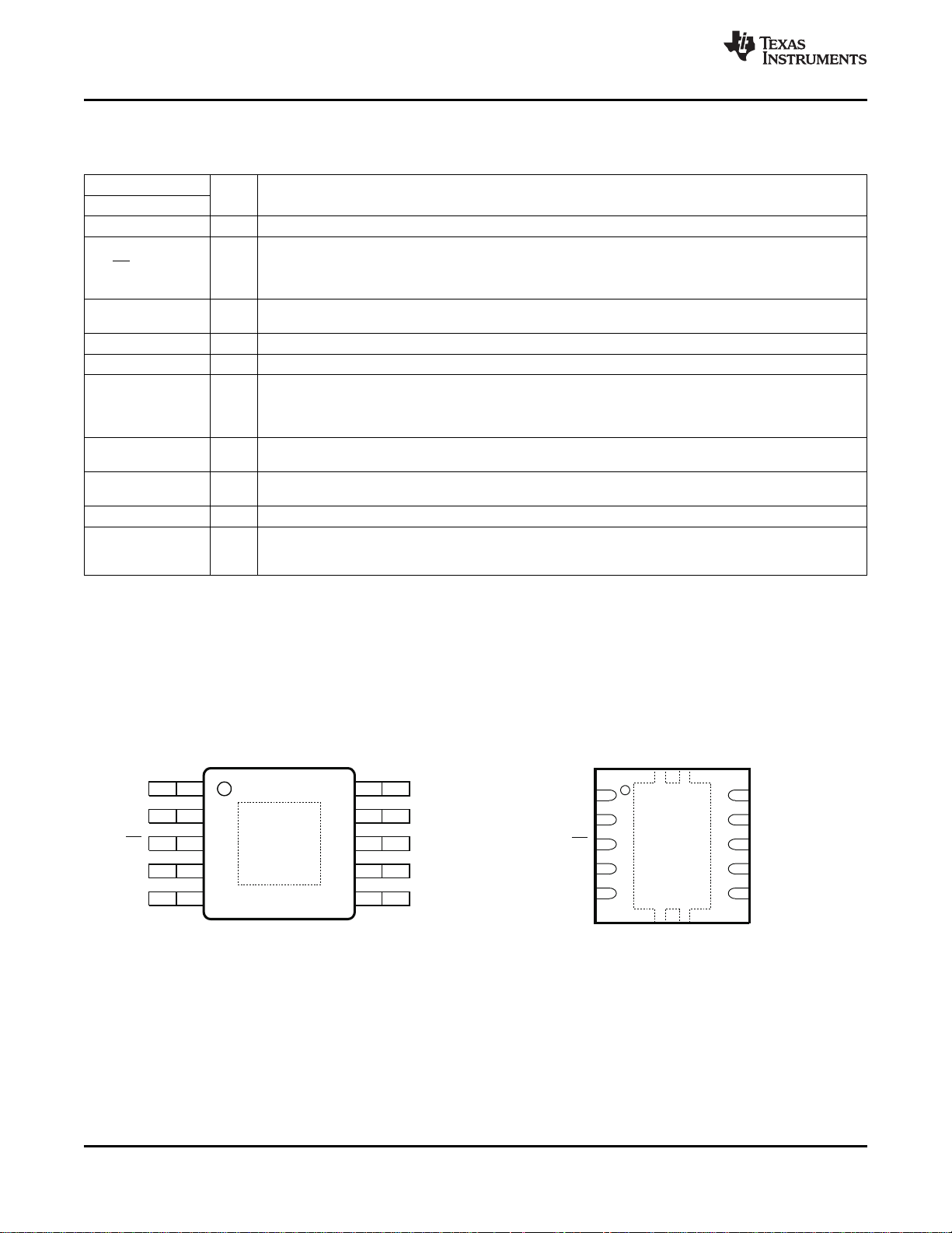
DEVICE INFORMATION
TERMINAL FUNCTIONS
TERMINAL
NAME NO.
COMP 4 O Error amplifier output. Connect control loop compensation network between COMP pin and FB pin.
DIS/ EN 3 I
FB 5 I
GDRV 8 O Connect the gate of the power N channel MOSFET to this pin.
GND 6 - Device ground.
ISNS 7 I
RC 1 I
SS 2 I
BP 9 O Regulator output pin. Connect a 1.0- µ F bypass capacitor from this pin to GND.
VDD 10 I required slope compensation, this pin can be connected to the converter output. See Application Information
I/O DESCRIPTION
Disable pin. Pulling this pin high, places the part into a shutdown mode. Shutdown mode is characterized by
a very low quiescent current. While in shutdown mode, the functionality of all blocks is disabled and the BP
regulator is shut down. This pin has an internal 1-M Ω pull-down resistor to GND. Leaving this pin
unconnected enables the device.
Error amplifier inverting input. Connect a voltage divider from the output to this pin to set output voltage.
Compensation network is connected between this pin and COMP.
Current sense pin. Connect an external current sensing resistor between this pin and GND. The voltage on
this pin is used to provide current feedback in the control loop and detect an overcurrent condition. An
overcurrent condition is declared when ISNS pin voltage exceeds the overcurrent threshold voltage, 150 mV
typical.
Switching frequency setting pin. Connect capacitor from RC pin to GND. Connect a resistor from RC pin
toVDD of the IC power supply and a capacitor from RC to GND.
Soft-start time programming pin. Connect capacitor from SS pin to GND to program converter soft-start time.
This pin also functions as a timeout timer when the power supply is in an overcurrent condition.
System input voltage. Connect a local bypass capacitor from this pin to GND. Depending on the amount of
section for additional details.
www.ti.com
10 Submit Documentation Feedback Copyright © 2008, Texas Instruments Incorporated
DGQ PowerPAD PACKAGE DRC PACKAGE
(TOP VIEW) (TOP VIEW)
Product Folder Link(s): TPS40210 TPS40211
+
+
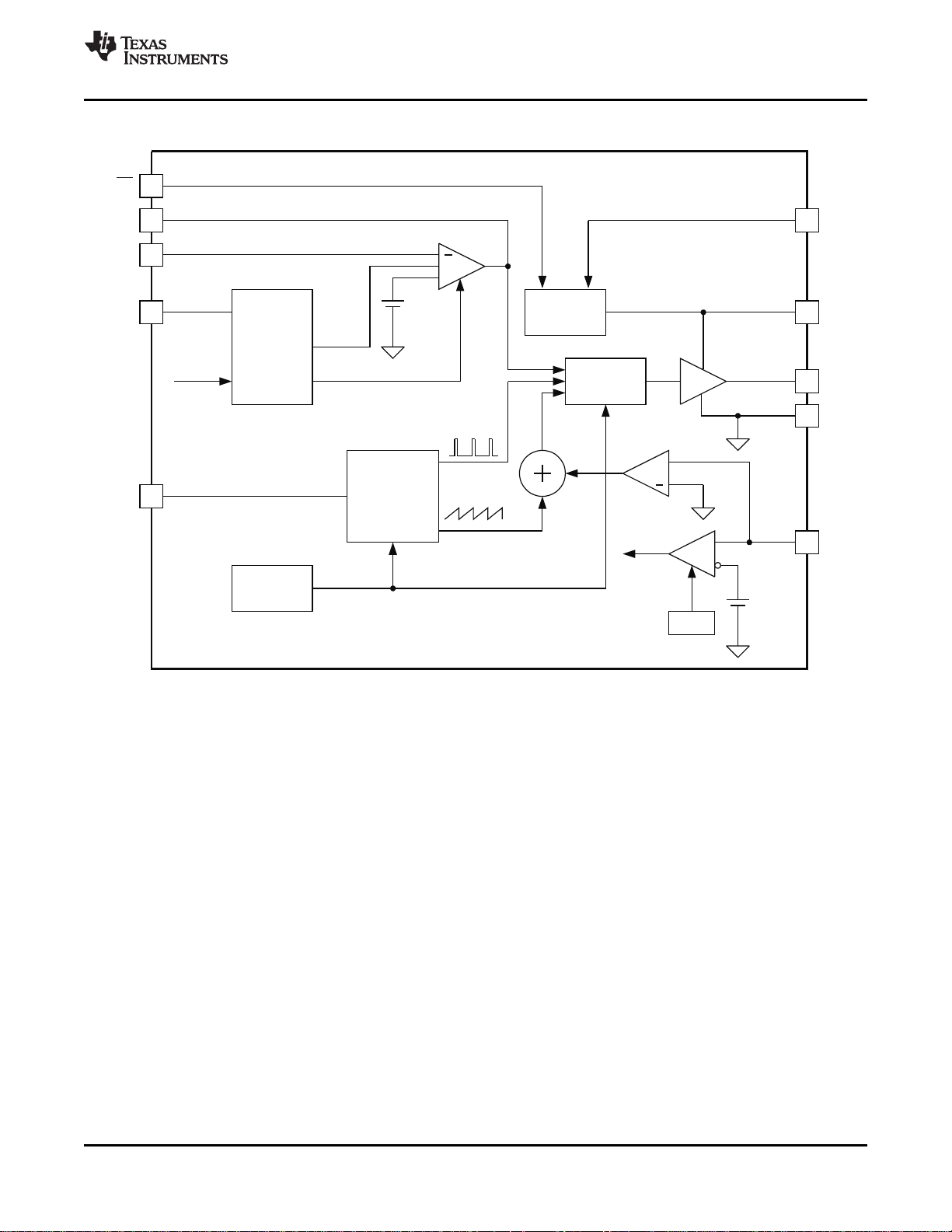
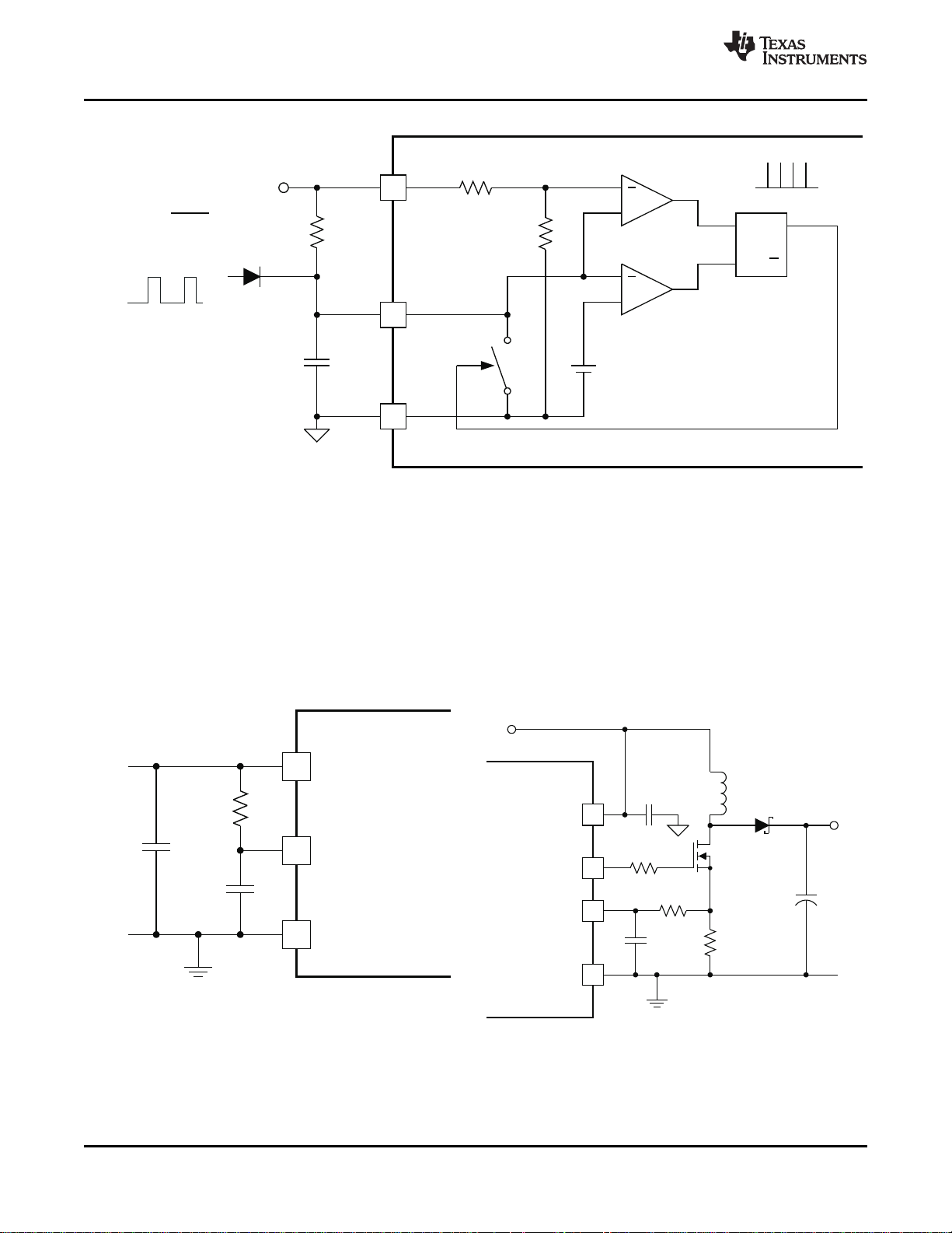
Soft Start
and
Overcurrent
5FB
4COMP
3DIS/EN
700 mV
LDO
PWM
Logic
2SS
1RC
Oscillator
and
Slope
Compensation
UVLO
Driver
9 BP
10 VDD
8 GDRV
6 GND
7 ISNS
+
Gain = 6
+
150 mV
LEB
OC Fault
OC Fault
UDG-07107
Enable E/A
E/A
SS Ref
TPS40210 , TPS40211
www.ti.com
.......................................................................................................................................................... SLUS772B – MARCH 2008 – REVISED JUNE 2008
FUNCTIONAL BLOCK DIAGRAM
Copyright © 2008, Texas Instruments Incorporated Submit Documentation Feedback 11
Product Folder Link(s): TPS40210 TPS40211

OUT D
IN
V V
1
V 1 D
+
=
-
IN
OUT D
V
D 1
V V
æ ö
æ ö
= -
ç ÷
ç ÷
ç ÷
+
è ø
è ø
( )
( )
f
OUT D OUT SW
2
IN
2 V V I L
D
V
´ + ´ ´ ´
=
( )
( )
( )
f
2
OUT D IN IN
OUT(crit)
2
OUT D SW
V V V V
I
2 V V L
+ - ´
=
´ + ´ ´
TPS40210 , TPS40211
SLUS772B – MARCH 2008 – REVISED JUNE 2008 ..........................................................................................................................................................
www.ti.com
APPLICATION INFORMATION
Minimum On-Time and Off Time Considerations
The TPS40210 has a minimum off time of approximately 200 ns and a minimum on time of 300 ns. These two
constraints place limitations on the operating frequency that can be used for a given input to output conversion
ratio. See Figure 2 for the maximum frequency that can be used for a given duty cycle.
The duty cycle at which the converter operates is dependent on the mode in which the converter is running. If the
converter is running in discontinuous conduction mode, the duty cycle varies with changes to the load much
more than it does when running in continuous conduction mode.
In continuous conduction mode, the duty cycle is related primarily to the input and output voltages.
In discontinuous mode the duty cycle is a function of the load, input and output voltages, inductance and
switching frequency.
(1)
(2)
All converters using a diode as the freewheeling or catch component have a load current level at which they
transition from discontinuous conduction to continuous conduction. This is the point where the inductor current
just falls to zero. At higher load currents, the inductor current does not fall to zero but remains flowing in a
positive direction and assumes a trapezoidal wave shape as opposed to a triangular wave shape. This load
boundary between discontinuous conduction and continuous conduction can be found for a set of converter
parameters as follows.
For loads higher than the result of Equation 4 , the duty cycle is given by Equation 2 and for loads less that the
results of Equation 4 , the duty cycle is given Equation 3 . For Equations 1 through 4, the variable definitions are
as follows.
• V
• V
• V
• I
is the output voltage of the converter in V
OUT
is the forward conduction voltage drop across the rectifier or catch diode in V
D
is the input voltage to the converter in V
IN
is the output current of the converter in A
OUT
• L is the inductor value in H
• fSWis the switching frequency in Hz
(3)
(4)
12 Submit Documentation Feedback Copyright © 2008, Texas Instruments Incorporated
Product Folder Link(s): TPS40210 TPS40211
T
8 10 2 7 4 6 9 2
SW T SW SW T T
1
R
5.8 10 f C 8 10 f 1.4 1 0 f 1.5 10 1.7 10 C 4 10 C
- - - - - -
=
´ ´ ´ + ´ ´ + ´ ´ - ´ + ´ ´ - ´ ´
+
1
RC
150 mV
S Q
QR
+
+
8
5
VDD
GND
R
RC
C
RC
CLK
External Frequency
Synchronization
(optional)
V
IN
TPS40210/11
UDG-08063
TPS40210 , TPS40211
www.ti.com
.......................................................................................................................................................... SLUS772B – MARCH 2008 – REVISED JUNE 2008
Setting the Oscillator Frequency
The oscillator frequency is determined by a resistor and capacitor connected to the RC pin of the TPS40210. The
capacitor is charged to a level of approximately V
/20 by current flowing through the resistor and is then
VDD
discharged by a transistor internal to the TPS40210. The required resistor for a given oscillator frequency is
found from either Figure 1 or Equation 5 .
where
• RTis the timing resistance in k Ω
• fSWis the switching frequency in kHz
• CTis the timing capacitance in pF
For most applications a capacitor in the range of 68 pF to 120 pF gives the best results. Resistor values should
be limited to between 100 k Ω and 1 M Ω as well. If the resistor value falls below 100 k Ω , decrease the capacitor
size and recalculate the resistor value for the desired frequency. As the capacitor size decreases below 47 pF,
the accuracy of Equation 5 degrades and empirical means may be needed to fine tune the timing component
values to achieve the desired switching frequency.
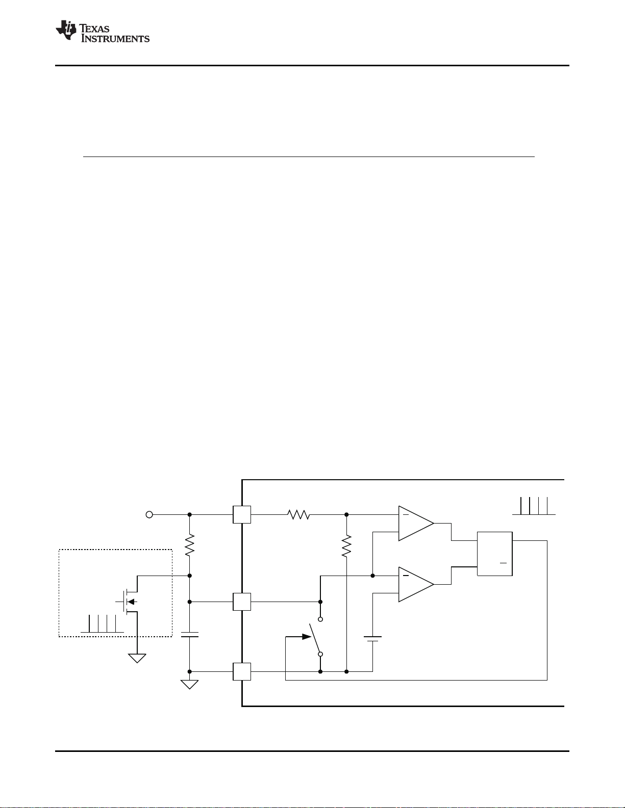
Synchronizing the Oscillator
The TPS40210 and TPS40211 can be synchronized to an external clock source. Figure 20 shows the functional
diagram of the oscillator. When synchronizing the oscillator to an external clock, the RC pin must be pulled below
150 mV for 20 ns or more. The external clock frequency must be higher than the free running frequency of the
converter as well. When synchronizing the controller, if the RC pin is held low for an excessive amount of time,
erratic operation may occur. The maximum amount of time that the RC pin should be held low is 50% of a
nominal output pulse, or 10% of the period of the synchronization frequency.
Under circumstances where the duty cycle is less than 50%, a Schottky diode connected from the RC pin to an
external clock may be used to synchronize the oscillator. The cathode of the diode is connected to the RC pin.
The trip point of the oscillator is set by an internal voltage divider to be 1/20 of the input voltage. The clock signal
must have an amplitude higher than this trip point. When the clock goes low, it allows the reset current to restart
the RC ramp, synchronizing the oscillator to the external clock. This provides a simple, single-component method
for clock synchronization.
(5)
Copyright © 2008, Texas Instruments Incorporated Submit Documentation Feedback 13
Figure 20. Oscillator Functional Diagram
Product Folder Link(s): TPS40210 TPS40211
+
1
RC
TPS40210/11
150 mV
S Q
QR
+
+
8
5
VDD
GND
R
RC
C
RC
CLK
Frequency > Controller
Frequency
V
IN
Amplitude >
20
V
IN
Duty Cycle < 50%
UDG-08064
10
1
6
TPS40210/11
VDD
RC
GND
C
T
R
T
UDG-07119
10
8
7
VDD
ISNS
GDRV
GND
TPS40210/11
L
V
OUT
V
IN
6
R
ISNS
UDG-07120
C
IFLT
R
IFLT
TPS40210 , TPS40211
SLUS772B – MARCH 2008 – REVISED JUNE 2008 ..........................................................................................................................................................
www.ti.com
Figure 21. Diode Connected Synchronization
Current Sense and Overcurrent
The tps40210 and TPS40211 are current mode controllers and use a resistor in series with the source terminal
power FET to sense current for both the current mode control and overcurrent protection. The device enters a
current limit state if the voltage on the ISNS pin exceeds the current limit threshold voltage V
electrical specifications table. When this happens the controller discharges the SS capacitor through a relatively
high impedance and then attempt to restart. The amount of output current that causes this to happen is
dependent on several variables in the converter.
The load current overcurrent threshold is set by proper choice of R
discontinuous mode the current sense resistor is found in Equation 6 .
14 Submit Documentation Feedback Copyright © 2008, Texas Instruments Incorporated
Product Folder Link(s): TPS40210 TPS40211
Figure 22. Oscillator Components Figure 23. Current Sense Components
ISNS(oc)
. If the converter is operating in
ISNS
from the

( )
f
f
SW ISNS(oc)
ISNS
SW OUT(oc) OUT D IN
L V
R
2 L I V V V
´ ´
=
´ ´ ´ ´ + -
( )
f
ISNS ISNS
ISNS
OUT
RIPPLE
OUT
IN
SW
V V
R
I
I
I
D V
1 D 2
1 D 2 L
= =
æ ö æ ö
æ ö
æ ö
´
+
+
ç ÷ ç ÷
ç ÷
ç ÷
ç ÷
-
è ø
- ´ ´
è ø
è ø
è ø
f
VDD
e SW
V
s
20
æ ö
= ´
ç ÷
è ø
( )
CS ISNS OUT D IN
A R V V V
m2
L
´ ´ + -
=
TPS40210 , TPS40211
www.ti.com
If the converter is operating in continuous conduction mode R
.......................................................................................................................................................... SLUS772B – MARCH 2008 – REVISED JUNE 2008
can be found in Equation 7 .
ISNS
where
• R
• V
• D is the duty cycle (from Equation 2 )
• fSWis the switching frequency in Hz
• V
• L is the value of the inductor in H
• I
• VDis the drop across the diode in Figure 23
is the value of the current sense resistor in Ω .
ISNS
is the overcurrent threshold voltage at the ISNS pin (from electrical specifications)
ISNS(oc)
is the input voltage to the power stage in V (see text)
IN
(oc) is the desired overcurrent trip point in A
OUT
The TPS40210/11 has a fixed undervoltage lockout (UVLO) that allows the controller to start at a typical input
voltage of 4.25 V. If the input voltage is slowly rising, the converter might have less than its designed nominal
input voltage available when it has reached regulation. As a result, this may decreases the apparent current limit
load current value and must be taken into consideration when selecting R
R
must be the value at which the converter finishes startup. The total converter output current at startup is
ISNS
. The value of V
ISNS
used to calculate
IN
the sum of the external load current and the current required to charge the output capacitor(s). See the Soft Start
section of this datasheet for information on calculating the required output capacitor charging current.
The topology of the standard boost converter has no method to limit current from the input to the output in the
event of a short circuit fault on the output of the converter. If protection from this type of event is desired, it is
necessary to use some secondary protection scheme such a fuse or rely on the current limit of the upstream
power source.
(6)
(7)
Current Sense and Sub-Harmonic Instability
A characteristic of peak current mode control results in a condition where the current control loop can exhibit
instability. This results in alternating long and short pulses from the pulse width modulator. The voltage loop
maintains regulation and dioes not oscillate, but the output ripple voltage increases. The condition occurs only
when the converter is operating in continuous conduction mode and the duty cycle is 50% or greater. The cause
of this condition is described in Texas Instruments literature number SLUA101, available at www.ti.com. The
remedy for this condition is to apply a compensating ramp from the oscillator to the signal going to the pulse
width modulator. In the TPS40210/11 the oscillator ramp is applied in a fixed amount to the pulse width
modulator. The slope of the ramp is given in Equation 8 .
To ensure that the converter does not enter into sub-harmonic instability, the slope of the compensating ramp
signal must be at least half of the down slope of the current ramp signal. Since the compensating ramp is fixed in
the TPS40210/11, this places a constraint on the selection of the current sense resistor.
The down slope of the current sense wave form at the pulse width modulator is described in Equation 9 .
Since the slope compensation ramp must be at least half, and preferably equal to the down slope of the current
sense waveform seen at the pulse width modulator, a maximum value is placed on the current sense resistor
Copyright © 2008, Texas Instruments Incorporated Submit Documentation Feedback 15
(8)
(9)
Product Folder Link(s): TPS40210 TPS40211

( )
f
VDD SW
ISNS(max)
OUT D IN
V L
R
60 V V V
´ ´
=
´ + -
f
ON
SW
D
t =
IFLT IFLT ON
R C 0.1 t´ = ´
TPS40210 , TPS40211
SLUS772B – MARCH 2008 – REVISED JUNE 2008 ..........................................................................................................................................................
www.ti.com
when operating in continuous mode at 50% duty cycle or greater. For design purposes, some margin should be
applied to the actual value of the current sense resistor. As a starting point, the actual resistor chosen should be
80% or less that the value calculated in Equation 10 . This equation calculates the resistor value that makes the
slope compensation ramp equal to one half of the current ramp downslope. Values no more than 80% of this
result would be acceptable.
where
• Seis the slope of the voltage compensating ramp applied to the pulse width modulator in V/s
• fSWis the switching frequency in Hz
• V
• m2 is the down slope of the current sense waveform seen at the pulse width modulator in V/s
• R
• V
• VDis the drop across the diode in Figure 23
is the voltage at the VDD pin in V
VDD
is the value of the current sense resistor in Ω
ISNS
is the converter output voltage V
OUT
is the converter power stage input voltage
IN
It is possible to increase the voltage compensation ramp slope by connecting the VDD pin to the output voltage
of the converter instead of the input voltage as shown in Figure 23 . This can help in situations where the
converter design calls for a large ripple current value in relation to the desired output current limit setting.
NOTE:
Connecting the VDD pin to the output voltage of the converter affects the startup
voltage of the converter since the controller undervoltage lockout (UVLO) circuit
monitors the VDD pin and senses the input voltage less the diode drop before startup.
The effect is to increase the startup voltage by the value of the diode voltage drop.
If an acceptable R
divided down to an acceptable level by placing another resistor in parallel with C
value is not available, the next higher value can be used and the signal from the resistor
ISNS
.
ISNS
(10)
Current Sense Filtering
In most cases, a small filter placed on the ISNS pin improves performance of the converter. These are the
components R
and C
IFLT
in Figure 23 . The time constant of this filter should be approximately 10% of the
IFLT
nominal pulse width of the converter. The pulse width can be found using Equation 11 .
The suggested time constant is then
The range of R
should be from about 1 k Ω to 5 k Ω for best results. Higher values can be used but this raises
IFLT
the impedance of the ISNS pin connection more than necessary and can lead to noise pickup issues in some
layouts. C
should be located as close as possible to the ISNS pin as well to provide noise immunity.
ISNS
Soft Start
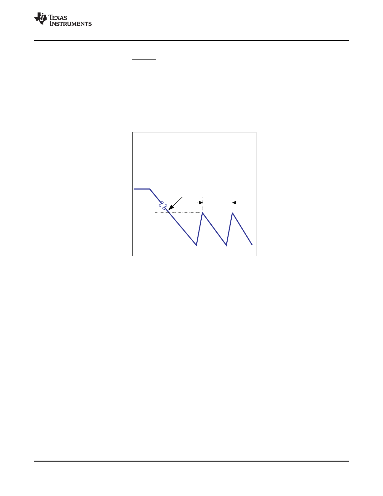
The soft-start feature of the TPS40210/11 is a closed loop soft start, meaning that the output voltage follows a
linear ramp that is proportional to the ramp generated at the SS pin. This ramp is generated by an internal
resistor connected from the BP pin to the SS pin and an external capacitor connected from the SS pin to GND.
The SS pin voltage (V
of the “ + ” (the “ + ” input with the lowest voltage dominates) inputs of the error amplifier. When this level shifted
voltage (V
Since V
) starts to rise at time t1(see Figure 24 ), the output voltage the controller expects, rises as well.
SSE
starts at near 0 V, the controller attempts to regulate the output voltage from a starting point of zero
SSE
volts. It cannot do this due to the converter architecture. The output voltage starts from the input voltage less the
) is level shifted down by approximately V
SS
(approximately 700 mV) and sent to one
SS(ofst)
(11)
(12)
16 Submit Documentation Feedback Copyright © 2008, Texas Instruments Incorporated
Product Folder Link(s): TPS40210 TPS40211

V
SSE(1)
V
SS
V
OUT
V
SSE
V
SS(ofst)
t
0
t
1
V
SS(ofst)
+700 mV
VIN- V
D
t2t
3
2
5
4
SS
COMP
FB
TPS40210/11
R
SS(chg)
UDG-07121
+
+
R
SS(dchg)
700 mV REF
OC Fault
UVLODIS
Error Amplifier
( )
SS
SS
BP SS(ofst)
SS
BP SS(ofst) FB
t
C
V V
R ln
V V V
=
æ ö
-
ç ÷
´
ç ÷
- +
è ø
TPS40210 , TPS40211
www.ti.com
drop across the diode (V
point where the V
voltage level is labeled V
.......................................................................................................................................................... SLUS772B – MARCH 2008 – REVISED JUNE 2008
- VD) and rise from there. The point at which the output voltage starts to rise (t2) is the
IN
ramp passes the point where it is commanding more output voltage than (V
SSE
. The time required for the output voltage to ramp from a theoretical zero to the
SSE(1)
- VD). This
IN
final regulated value (from t1to t3) is determined by the time it takes for the capacitor connected to the SS pin
(C
) to rise through a 700 mV range, beginning at V
SS
above GND.
SS(ofst)
The required capacitance for a given soft start time t3– t1in Figure 24 is calculated in Equation 13 .
Figure 24. SS Pin Voltage adn Output Voltage Figure 25. SS Pin Functional Circuit
where
• tSSis the soft-start time
• R
• C
• V
• V
Note that tSSis the time it takes for the output voltage to rise from 0 V to the final output voltage. Also note the
tolerance on R
voltage rise time and margin must be applied to account for it in design.
Copyright © 2008, Texas Instruments Incorporated Submit Documentation Feedback 17
• V
is the SS charging resistance in Ω , typically 500 k Ω
SS(chg)
is the value of the capacitor on the SS pin, in F
SS
is the value of the voltage on the BP pin in V
BP
is the approximate level shift from the SS pin to the error amplifier (~700 mV)
SS(ofst)
is the error amplifier reference voltage, 700m V typical
FB
SS(chg)
given in the electrical specifications table. This contributes to some variability in the output
Product Folder Link(s): TPS40210 TPS40211
(13)

OUT
C(chg)
SS
C
I
t
æ ö
=
ç ÷
è ø
( )
OUT
SS
OUT(oc ) EXT
C
t
I I
æ ö
ç ÷
>
ç ÷
-
è ø
TPS40210 , TPS40211
SLUS772B – MARCH 2008 – REVISED JUNE 2008 ..........................................................................................................................................................
Also take note of V
. Its value varies depending on input conditions. For example, a converter operating from a
BP
slowly rising input initializes V
at a fairly low value and increases during the entire startup sequence. If the
BP
www.ti.com
controller has a voltage above 8 V at the input and the DIS pin is used to stop and then restart the converter, V
is approximately 8 V for the entire startup sequence. The higher the voltage on BP, the shorter the startup time is
and conversely, the lower the voltage on BP, the longer the startup time is.
The soft-start time (t
) must be chosen long enough so that the converter can start up without going into an
SS
overcurrent state. Since the over current state is triggered by sensing the peak voltage on the ISNS pin, that
voltage must be kept below the overcurrent threshold voltage V
. The voltage on the ISNS pin is a function
ISNS(oc)
of the load current of the converter, the rate of rise of the output voltage and the output capacitance, and the
current sensing resistor. The total output current that must be supported by the converter is the sum of the
charging current required by the output capacitor and any external load that must be supplied during startup. This
current must be less than the I
value used in Equation 6 or Equation 7 (depending on the operating mode
OUT(oc)
of the converter) to determine the current sense resistor value. In these equations, the actual input voltage at the
time that the controller reaches the final output voltage is the important input voltage to use in the calculations. If
the input voltage is slowly rising and is at less than the nominal input voltage when the startup time ends, the
output current limit is less than I
be reduced (decrease C
OUT
OUT(oc)
or increase the tSS) or I
at the nominal input voltage. The output capacitor charging current must
OUT(oc)
must be increased and a new value for R
calculated.
BP
ISNS
(14)
where
• I
• C
• tSSis the soft start time from Equation 13
• I
• I
The capacitor on the SS pin (C
restart attempts. The SS pin is connected to GND through a resistor, R
is the output capacitor charging current in A
C(chg)
is the total output capacitance in F
OUT
is the desired over current trip point in A
OUT(oc)
is any external load current in A
EXT
) also plays a role in overcurrent functionality. It is used as the timer between
SS
, whenever the controller senses an
SS(dchg)
overcurrent condition. Switching stops and nothing else happens until the SS pin discharges to the soft-start
reset threshold, V
resistor R
, and the controller restarts from that point. The shortest time between restart attempts occurs
SS(chg)
when the SS pin discharges from V
. At this point, the SS pin capacitor is allowed to charge again through the charging
SS(rst)
(approximately 700 mV) to V
SS(ofst)
(150 mV) and then back to V
SS(rst)
and switching resumes. In actuality, this is a conservative estimate since switching does not resume until the
V
ramp rises to a point where it is commanding more output voltage than exists at the output of the controller.
SSE
This occurs at some SS pin voltage greater than V
and depends on the voltage that remains on the output
SS(ofst)
overvoltage the converter while switching has been halted. The fastest restart time can be calculated by using
Equation 16 , Equation 17 and Equation 18 .
(15)
SS(ofst)
18 Submit Documentation Feedback Copyright © 2008, Texas Instruments Incorporated
Product Folder Link(s): TPS40210 TPS40211
SS(ofst)
DCHG SS(dchg) SS
SS(rst)
V
t R C ln
V
æ ö
ç ÷
= ´ ´
ç ÷
è ø
( )
( )
BP SS(rst)
CHG SS(chg) SS
BP SS(ofst)
V V
t R C ln
V V
æ ö
-
ç ÷
= ´ ´
ç ÷
-
è ø
( )
CHG DCHG
RSTRT min
t t t= +
t
RSTR(min)
V
SS(ofst)
V
SS
V
BP
V
SS(rst)
T - Time
TPS40210 , TPS40211
www.ti.com
.......................................................................................................................................................... SLUS772B – MARCH 2008 – REVISED JUNE 2008
(16)
(17)
(18)
Figure 26. Soft Start During Overcurrent
Copyright © 2008, Texas Instruments Incorporated Submit Documentation Feedback 19
Product Folder Link(s): TPS40210 TPS40211

Q VDD VDD(en)
P V I= ´
f
G VDD g SW
P V Q= ´ ´
E VDD EXT
P V I= ´
TPS40210 , TPS40211
SLUS772B – MARCH 2008 – REVISED JUNE 2008 ..........................................................................................................................................................
www.ti.com
BP Regulator
The TPS40210/11 has an on board linear regulator the supplies power for the internal circuitry of the controller,
including the gate driver. This regulator has a nominal output voltage of 8 V and must be bypassed with a 1- µ F
capacitor. If the voltage at the VDD pin is less than 8 V, the voltage on the BP pin ia also be less and the gate
drive voltage to the external FET ia reduced from the nominal 8 V. This should be considered when choosing a
FET for the converter.
Connecting external loads to this regulator can be done, but care must be taken to ensure that the thermal rating
of the device is observed since is no thermal shutdown feature in this controller. Exceeding the thermal ratings
cause out of specification behavior and can lead to reduced reliability. The controller dissipates more power
when there is an external load on the BP pin and is tested for dropout voltage for up to 5-mA load. When the
controller is in the disabled state, the BP pin regulator also shuts off so loads connected there power down as
well. When the controller is disabled with the DIS/ EN pin, this regulator is turned off.
The total power dissipation in the controller can be calculated as follows. The total power is the sum of PQ, P
and PE.
where
• PQis the quiescent power of the device in W
• V
• I
• PGis the power dissipated by driving the gate of the FET in W
• Qgis the total gate charge of the FET at the voltage on the BP pin in C
• fSWis the switching frequency in Hz
• PEis the dissipation caused be external loading of the BP pin in W
• I
is the VDD pin voltage in V
VDD
is the quiescent current of the controller when enabled but not switching in A
VDD(en)
is the external load current in A
EXT
G
(19)
(20)
(21)
Shutdown (DIS/ EN Pin)
The DIS/ EN pin is an active high shutdown command for the controller. Pulling this pin above 1.2 V causes the
controller to completely shut down and enter a low current consumption state. In this state, the regulator
connected to the BP pin is turned off. There is an internal 1.1-M Ω pull-down resistor connected to this pin that
keeps the pin at GND level when left floating. If this function is not used in an application, it is best to connect
this pin to GND
20 Submit Documentation Feedback Copyright © 2008, Texas Instruments Incorporated
Product Folder Link(s): TPS40210 TPS40211

1
2
3
4
10
9
8
7
RC
DIS/EN
COMP
SS
VDD
ISNS
GDRV
GND
TPS40210
C
FB
L
C
OUT
R
OUT
V
OUT
V
IN
5 FB 6
BP
R
FB
R
SENSE
UDG-07177
R
IFLT
C
IFLT
C
HF
R
1
R
2
TPS40210 , TPS40211
www.ti.com
.......................................................................................................................................................... SLUS772B – MARCH 2008 – REVISED JUNE 2008
Control Loop Considerations
There are two methods to design a suitable control loop for the TPS4021x. The first and preferred if equipment is
available is to use a frequency response analyzer to measure the open loop modulator and power stage gain
and to then design compensation to fit that. The usage of these tools for this purpose is well documented with
the literature that accompanies the tool and is not be discussed here.
The second option is to make an initial guess at compensation, and then evaluate the transient response of the
system to see if the compensation is acceptable to the application or not. For most systems, an adequate
response can be obtained by simply placing a series resistor and capacitor (R
the FB pin as shown in Figure 27 .
and C
FB
) from the COMP pin to
FB
Figure 27. Basic Compensation Network
The natural phase characteristics of most capacitors used for boost outputs combined with the current mode
control provide adequate phase margin when using this type of compensation. To determine an initial starting
point for the compensation, the desired crossover frequency must be considered when estimating the control to
output gain. The model used is a current source into the output capacitor and load.
When using these equations, the loop bandwidth should be no more than 20% of the switching frequency, fSW. A
more reasonable loop bandwidth would be 10% of the switching frequency. Be sure to evaluate the transient
response of the converter over the expected load range to ensure acceptable operation.
Copyright © 2008, Texas Instruments Incorporated Submit Documentation Feedback 21
Product Folder Link(s): TPS40210 TPS40211

( )
f
CO M OUT CO
A
K g Z 19.1 0.146 2.80
V
= ´ = ´ W =
( ) ( )
( ) ( )
f
f
SW
OUT
M
2 2
ISNS ISNS SW
600kHz
0.13 L
0.13 10 H
R
240
A
g 19.1
V
12m 120 12m 10 H 600kHz
R 120 R L
´ ´
´ m ´
W
= = =
W ´ ´ W + m ´
´ ´ + ´
( )
( )
( ) ( )
( )
( )
2
L ESR OUT
OUT OUT
2 2 2
OUT OUT ESR ESR L OUT
1 2 f R C
Z R
1 R 2 R R R 2 f C
+ p´ ´ ´
= ´
+ + ´ ´ + ´ p ´ ´
COMP
CO
1 1
K 0.356
K 2.80
= = =
FB COMP
CO
R1
R R1 K
K
= = ´
FB
L FB
10
C
2 f R
=
p´ ´
TPS40210 , TPS40211
SLUS772B – MARCH 2008 – REVISED JUNE 2008 ..........................................................................................................................................................
www.ti.com
where
• K
• gMis the transconductance of the power stage and modulator, in S
• R
• Z
• R
• L is the value of the inductor, in H
• C
• R
• fSWis the switching frequency, in Hz
• fLis the desired crossover frequency for the control loop, in Hz
is the control to output gain of the converter, in V/V
CO
is the output load equivalent resistance, in Ω
OUT
is the output impedance, including the output capacitor, in Ω
OUT
is the value of the current sense resistor, in Ω
ISNS
is the value of the output capacitance, in µ F
OUT
is the equivalent series resistance of C
ESR
, in Ω
OUT
These equations assume that the operation is discontinuous and that the load is purely resistive. The gain in
continuous conduction can be found by evaluating Equation 23 at the resistance that gives the critical conduction
current for the converter. Loads that are more like current sources give slightly higher gains than predicted here.
To find the gain of the compensation network required for a control loop of bandwidth fL, take the reciprocal of
Equation 22 .
(22)
(23)
(24)
The GBWP of the error amplifier is only guaranteed to be at least 1.5 MHz. If K
than 750 kHz, reduce the desired loop crossover frequency until this condition is satisfied. This ensures that the
high-frequency pole from the error amplifier response with the compensation network in place does not cause
excessive phase lag at the fLand decrease phase margin in the loop.
The R-C network connected from COMP to FB places a zero in the compensation response. That zero should be
approximately 1/10th of the desired crossover frequency, fL. With that being the case, R
from Equation 26 and Equation 27
where
• R1 is in fLis the loop crossover frequency desired, in Hz
• R
is the feedback resistor in C
FB
is the feedback capacitance in µ F.
FB
Thought not strictly necessary, it is recommended that a capacitor be added between COMP and FB to provide
high-frequency noise attenuation in the control loop circuit. This capacitor introduces another pole in the
compensation response. The allowable location of that pole frequency determines the capacitor value. As a
starting point, the pole frequency should be 10 × fL. The value of C
22 Submit Documentation Feedback Copyright © 2008, Texas Instruments Incorporated
Product Folder Link(s): TPS40210 TPS40211
can be found from Equation 28 .
HF
multiplied by the fLis greater
COMP
(25)
and C
FB
can be found
FB
(26)
(27)

HF
L FB
1
C
20 f R
=
p´ ´
( )
HF
6
FB
1
C
2 1.5 10 R
=
p´ ´ ´
G
G
105
RQ=
10
8
7
6
VDD
GDRV
ISNS
GND
TPS40210/11
L
V
IN
R
G
V
OUT
UDG-07196
TPS40210 , TPS40211
www.ti.com
.......................................................................................................................................................... SLUS772B – MARCH 2008 – REVISED JUNE 2008
The error amplifier GBWP will usually be higher, but is ensured by design to be at least 1.5 MHz. If the gain
required in Equation 25 multiplied by 10 times the desired control loop crossover frequency, the high-frequency
pole introduced by C
If this is the case, C
design. Equation 29 calculates the required C
is overridden by the error amplifier capability and the effective pole is lower in frequency.
HF
can be made larger to provide a consistent high-frequency roll off in the control loop
HF
in this case.
HF
where
• C
• R
is the high-frequency roll-off capacitor value in µ F
HF
is the mid band gain setting resistor value in Ω
FB
GATE DRIVE CIRCUIT
Some applications benefit from the addition of a resistor connected between the GDRV pin and the gate of the
switching MOSFET. In applications that have particularly stringent load regulation (under 0.75%) requirements
and operate from input voltages above 5 V, or are sensitive to pulse jitter in the discontinuous conduction region,
this resistor is recommended. The recommended starting point for the value of this resistor can be calculated
from Equation 30 .
(28)
(29)
(30)
where
• Q
is the MOSFET total gate charge at 8-V V
G
• R
is the suggested starting point gate resistance in Ω
G
Figure 28. Gate Drive Resistor
in nC
GS
Copyright © 2008, Texas Instruments Incorporated Submit Documentation Feedback 23
Product Folder Link(s): TPS40210 TPS40211

10
9
8
7
VDD
BP
ISNS
GDRV
TPS40210/11
L
V
IN
UDG-07197
6GND
R
IFB
1
2
3
4
5
RC
SS
COMP
DIS/EN
FB
I
OUT
FB
IFB
OUT
V
RI=
TPS40210 , TPS40211
SLUS772B – MARCH 2008 – REVISED JUNE 2008 ..........................................................................................................................................................
www.ti.com
TPS40211
The only difference between the TPS40210 and the TPS40211 is the reference voltage that the error amplifier
uses to regulate the output voltage. The TPS40211 uses a 260-mV reference and is intended for applications
where the output is actually a current instead of a regulated voltage. A typical example of an application of this
type is an LED driver. An example schematic is shown in Figure 29 .
Figure 29. Typical LED Drive Schematic
The current in the LED string is set by the choice of the resistor R
where
• R
• V
• I
is the value of the current sense resistor for the LED string in Ω
IFB
is the reference voltage for the TPS40211 in V (0.260 V typ)
FB
is the desired DC current in the LED string in A
OUT
as shown in Equation 31 .
ISNS
(31)
24 Submit Documentation Feedback Copyright © 2008, Texas Instruments Incorporated
Product Folder Link(s): TPS40210 TPS40211

TPS40210 , TPS40211
www.ti.com
.......................................................................................................................................................... SLUS772B – MARCH 2008 – REVISED JUNE 2008
ADDITIONAL REFERENCES
Related Devices
The following devices have characteristics similar to the TPS40210 and may be of interest.
Related Parts
DEVICE DESCRIPTION
TPS6100X Single- and Dual-Cell Boost Converter with Strart-up into Full Load
TPS6101X High Efficiency 1-Cell and 2-Cell Bost Converters
TPS6300X High Effiency Single Inductor Buck-Boost Converter with 1.8A Switches
References
These references may be found on the web at www.power.ti.com under Technical Documents. Many design
tools and links to additional references, may also be found at www.power.ti.com
1. Design and Application Guide for High Speed MOSFET Gate Drive Circuits, SEM 1400, 2001 Seminar
Series
2. Designing Stable Control Loops, SEM 1400, 2001 Seminar Series
3. Additional PowerPAD
4. QFN/SON PCB Attachment, Texas Instruments Literature Number SLUA271, June 2002
TM
information may be found in Applications Briefs SLMA002 and SLMA004
Copyright © 2008, Texas Instruments Incorporated Submit Documentation Feedback 25
Product Folder Link(s): TPS40210 TPS40211

+
+
TPS40210 , TPS40211
SLUS772B – MARCH 2008 – REVISED JUNE 2008 ..........................................................................................................................................................
DESIGN EXAMPLE 1
12-V to 24-V Non-Synchronous Boost Regulator
The following example illustrates the design process and component selection for a 12-V to 24-V
non-synchronous boost regulator using the TPS40210 controller.
www.ti.com
Figure 30. TPS40210 Design Example – 8-V to 24-V at 2-A
TPS40210 Design Example Specifications
PARAMETER CONDITIONS MIN NOM MAX UNIT
INPUT CHARACTERISTICS
V
IN
I
IN
V
IN(UVLO)
OUTPUT CHARACTERISTICS
V
OUT
V
OUT(ripple)
I
OUT
I
OCP
Δ I Load step 1 A
Input voltage 8 12 14 V
Input current 4.4
No load input current 0.05
Input undervoltage lockout 4.5 V
Output voltage 23.5 24.0 24.5 V
Line regulation 1%
Load regulation 1%
Output voltage ripple 500 mV
Output current 8 V ≤ VIN≤ 14 V 0.2 1 2.0
Output overcurrent inception point 3.5
Transient response
Load slew rate 1 A/ µ s
Overshoot threshold voltage 500 mV
Settling time 5 ms
A
PP
A
26 Submit Documentation Feedback Copyright © 2008, Texas Instruments Incorporated
Product Folder Link(s): TPS40210 TPS40211

OUT IN(max) FD
MIN
OUT FD
V V V
24 V 14 V 0.5 V
D 42.8%
V V 24 V 0.5 V
- +
- +
» = =
+ +
OU T IN(m in ) FD
MA X
OU T FD
V V V
24 V 8 V 0.5 V
D 67.3%
V V 2 4 V 0.5 V
- +
- +
» = =
+ +
OU T(ma x)
Lrip(m ax)
MIN
I
2
I 0.3 0.3 1.05 A
1 D 1 0.428
= ´ = ´ =
- -
f
IN(max)
MIN MIN
Lrip(max) SW
V
1 14 V 1
L D 0.673 9.5 H
I 1.05 A 600kHz
» ´ ´ = ´ ´ = m
f
IN
RIP PL E
SW
V
1 12 V 1
I D 0.50 1.02 A
L 10 H 600 kHz
» ´ ´ = ´ ´ =
m
f
IN
RIPPLE(Vinmin)
SW
V
1 8 V 1
I D 0.673 0.89 A
L 10 H 600 kHz
» ´ ´ = ´ ´ =
m
( )
(
)
( )
( )
( )
( )
2
2
2
2
2
2
OUT(max)
1 1 1
Lrms RIPPLE RIPPLE(VINmin)
L avg
12 12 12
MAX
I
2
I I I I 0.817A 6.13 Arms
1 D 1 0.673
æ ö
æ ö
= + » + = + ´ =
ç ÷
ç ÷
ç ÷
- -
è ø
è ø
TPS40210 , TPS40211
www.ti.com
.......................................................................................................................................................... SLUS772B – MARCH 2008 – REVISED JUNE 2008
TPS40210 Design Example Specifications (continued)
PARAMETER CONDITIONS MIN NOM MAX UNIT
SYSTEM CHARACTERISTICS
f
SW
η
PK
η Full load efficiency VIN= 12 V, I
T
OP
MECHANICAL DIMENSIONS
W Width 1.5
L Length 1.5 in
h Height 0.5
Switching frequency 600 kHz
Peak efficiency VIN= 12 V, 0.2 A ≤ I
OUT
Operating temperature range 10 V ≤ VIN≤ 14 V, 0.2 A ≤ I
≤ 2 A 95%
OUT
= 2 A 94%
≤ 2 A 25 ° C
OUT
Step-By-Step Design Procedure
Duty Cycle Estimation
The duty cycle of the main switching MOSFET is estimated using Equation 32 and Equation 33 .
(32)
Using and estimated forward drop of 0.5 V for a schottkey rectifier diode, the approximate duty cycle is 42.8%
(minimum) to 67.3% (maximum).
Inductor Selection
The peak-to-peak ripple is limited to 30% of the maximum output current.
The minimum inductor size can be estimated using Equation 35 .
The next higher standard inductor value of 10 µ H is selected. The ripple current is estimated by Equation 36 .
The worst case peak-to-peak ripple current occurs at 50% duty cycle and is estimated as 1.02 A. Worst case
RMS current through the inductor is approximated by Equation 38 .
(33)
(34)
(35)
(36)
(37)
The worst case RMS inductor current is 6.13 Arms. The peak inductor current is estimated by Equation 39 .
Copyright © 2008, Texas Instruments Incorporated Submit Documentation Feedback 27
Product Folder Link(s): TPS40210 TPS40211
(38)

( ) ( )
OUT(max)
1 1
Lpeak RIPPLE(Vin min)
2 2
MAX
I
2
I I 0.718 6.57 A
1 D 1 0.673
» + = + =
- -
( )
2
L Lrms
P I DCR» ´
OUT
(BR)R(min) OUT
V
V 1.25 V 1.25 24 V 30 V
0.8
³ = ´ = ´ =
( ) ( )
D avg OUT m ax
I I 2 A» =
( ) ( )
D peak L peak
I I 6.57 A= =
D(max) F OUT(max)
P V I 0.5 V 2 A 1W» ´ = ´ =
f
OUT
OUT
OUT(ripple) SW
I D
1 2 A 0.673 1
C 8 8 35 F
V 500 mV 600kHz
´
æ ö
´
= ´ = ´ = m
ç ÷
è ø
( )
( )
OUT ripple
OUT
L peak
V
7 7 500 mV
ESR 95 m
8 I I 8 6.57 A 2 A
= ´ = ´ = W
- -
TPS40210 , TPS40211
SLUS772B – MARCH 2008 – REVISED JUNE 2008 ..........................................................................................................................................................
www.ti.com
A 10- µ H inductor with a minimum RMS current rating of 6.13 A and minimum saturation current rating of 6.57 A
must be selected. A TDK RLF12560T-100M-7R5 7.5-A 10- µ H inductor is selected.
This inductor power dissipation is estimated by Equation 40 .
The TDK RLF12560T-100M-7R5 12.4-m Ω DCR dissipates 466 mW of power.
Rectifier Diode Selection
A low-forward voltage drop schottky diode is used as a rectifier diode to reduce its power dissipation and improve
efficiency. Using 80% derating, on V
for ringing on the switch node, the rectifier diode minimum reverse
OUT
break-down voltage is given by Equation 41 .
The diode must have reverse breakdown voltage greater than 30 V. The rectifier diode peak and average
currents are estimated by Equation 42 and Equation 43 .
(39)
(40)
(41)
(42)
For this design, 2-A average and 6.57-A peak is
The power dissipation in the diode is estimated by Equation 44 .
For this design, the maximum power dissipation is estimated as 1 W. Reviewing 30-V and 40-V schottky diodes,
the MBRS340T3, 40-V, 3-A diode in an SMC package is selected. This diode has a forward voltage drop of
0.48-V at 6-A, so the conduction power dissipation is approximately 960 mW, less than half its rated power
dissipation.
Output Capacitor Selection
Output capacitors must be selected to meet the required output ripple and transient specifications.
A Panasonic EEEFC1V330P 35V 33- µ F, 120-m Ω bulk capacitor and 6.8- µ F ceramic capacitor is selected to
provide the required capacitance and ESR at the switching frequency. The combined capacitance of 39.8 µ F and
60 m Ω are used in compensation calculations.
(43)
(44)
(45)
(46)
Input Capacitor Selection
Since a boost converter has continuous input current, the input capacitor senses only the inductor ripple current.
The input capacitor value can be calculated by Equation 47 and Equation 48 .
28 Submit Documentation Feedback Copyright © 2008, Texas Instruments Incorporated
Product Folder Link(s): TPS40210 TPS40211

( )
( )
f
L ripple
IN
SW
IN ripple
I
1.02 A
C 7.0 F
4 V 4 60 mV 600 kHz
> = = m
´ ´ ´ ´
( )
( )
IN ripple
L ripple
V
60mV
ESR 30 m
2 I 2 1.02 A
< = = W
´ ´
( )
(
)
OCP(min)
ISNS
Drive
L peak
V
110mV
R 14.2m
1.1 6.57 A 0.50 A
1.1 I I
< = = W
´ +
´ +
f
MAX SW
ISNS
OUT fd IN
VDD L
14 V 10 H 600kHz
R 133m
60 ( V V V ) 60 (24 V 0.48 V 14 V)
´ ´
´ m ´
< = = W
´ + - ´ + -
f
MIN
IFLT
SW IFLT
0.1 D
0.1 0.428
C 71pF
R 600kHz 1k
´
´
= = =
´ ´ W
DISS(total) OUT OUT OUT
1 1 1
P P 1 V I 1 24 V 2A 1 2.526 W
0.95
æ ö æ ö
æ ö
» ´ - = ´ ´ - = ´ ´ - =
ç ÷ ç ÷
ç ÷
h h
è ø
è ø è ø
( )
FET L D Risns IN(max) VDD
DISS total
P P P P P V I< - - - - ´
f
FET DRIVE
GS
OUT OUT SW
3 P I
3 0.50 W 0.50 A
Q 13.0nC
2 V I 2 24 V 2 A 600kHz
´ ´
´ ´
< = =
´ ´ ´ ´ ´ ´
TPS40210 , TPS40211
www.ti.com
.......................................................................................................................................................... SLUS772B – MARCH 2008 – REVISED JUNE 2008
For this design, to meet a maximum input ripple of 60 mV, a minimum 7.0- µ F input capacitor with ESR less than
30 m Ω is needed. A 10- µ F X7R ceramic capacitor is selected.
Current Sense and Current Limit
The maximum allowable current sense resistor value is limited by both the current limit and sub-harmonic
stability. These two limitations are given by Equation 49 and Equation 50 .
The current limit requires a resistor less than 14.2 m Ω and stability requires a sense resistor less than 133 m Ω . A
10-m Ω resistor is selected. Approximately 2-m Ω of routing resistance added in compensation calculations.
(47)
(48)
(49)
(50)
Current Sense Filter
To remove switching noise from the current sense, an R-C filter is placed between the current sense resistor and
the ISNS pin. A resistor with a value between 1 k Ω and 5 k Ω is selected and a capacitor value is calculated by
Equation 51 .
For a 1-k Ω filter resistor, 71 pF is calculated and a 100-pF capacitor is selected.
Switching MOSFET Selection
The TPS40210 drives a ground referenced N-channel FET. The R
and gate charge are estimated based on
DS(on)
the desired efficiency target.
For a target of 95% efficiency with a 24 V Input voltage at 2 A, maximum power dissipation is limited to 2.526 W.
The main power dissipating devices are the MOSFET, inductor, diode, current sense resistor and the integrated
circuit, the TPS40210.
This leaves 740 mW of power dissipation for the MOSFET. This can likely cause an SO-8 MOSFET to get too
hot, so power dissipation is limited to 500 mW. Allowing half for conduction and half for switching losses, we can
determine a target R
and Q
DS(on)
for the MOSFET by Equation 54 and Equation 55 .
GS
(51)
(52)
(53)
A target MOSFET gate-to-source charge of less than 13.0 nC is calculated to limit the switching losses to less
than 250 mW.
Copyright © 2008, Texas Instruments Incorporated Submit Documentation Feedback 29
Product Folder Link(s): TPS40210 TPS40211
(54)

( )
( )
FET
DS on
2 2
RMS
P
0.50 W
R 9.8m
2 6.13 0.674
2 I D
< = = W
´ ´
´ ´
FB FB
BIAS
OUT FB
V R
0.700 V 51.1k
R 1.53k
V V 24 V 0.700 V
´
´ W
= = = W
- -
( )
( )
OUT
OUT max
OUT min
V
24 V
R 240
I 0.1A
= = = W
( ) ( )
( ) ( )
f
f
SW
OUT
M
2 2
ISNS ISNS SW
600kHz
0.13 L
0.13 10 H
R
240
A
g 19.1
V
12m 120 12m 10 H 600kHz
R 120 R L
´ ´
´ m ´
W
= = =
W ´ ´ W + m ´
´ ´ + ´
( )
( )
( ) ( )
( )
( )
f
2
ESR OUT
OUT OUT
2 2 2
OUT OUT ESR ESR OUT
1 2 f R C
Z ( ) R
1 R 2 R R R 2 f C
+ p´ ´ ´
= ´
+ + ´ ´ + ´ p ´ ´
( )
( )
( )
( ) ( )
( )
( )
2
f
OUT CO
2 2 2
1 2 20kHz 60m 39.8 F
Z 240 0.146
1 240 2 240 60 m 60m 2 20kHz 39.8 F
+ p´ ´ W´ m
= W ´ = W
+ W + ´ W ´ W + W ´ p ´ ´ m
( )
f
CO M OUT CO
A
K g Z 19.1 0.146 2.80
V
= ´ = ´ W =
TPS40210 , TPS40211
SLUS772B – MARCH 2008 – REVISED JUNE 2008 ..........................................................................................................................................................
A target MOSFET R
30-V and 40-V MOSFETs, an Si4386DY 9-m Ω MOSFET is selected. A gate resistor was added per equation
(30). The maximum gate charge at Vgs=8 V for the Si4386DY is 33.2 nC, this impiles RG = 3.3 Ω .
Feedback Divider Resistors
The primary feedback divider resistor (R
maintain a balance between power dissipation and noise sensitivity. For a 24-V output a high feedback
resistance is desirable to limit power dissipation so R
R
= 1.50 k Ω is selected.
BIAS
Error Amplifier Compensation
While current mode control typically only requires Type II compensation, it is desirable to layout for Type III
compensation to increase flexibility during design and development.
Current mode control boost converters have higher gain with higher output impedance, so it is necessary to
calculate the control loop gain at the maximum output impedance, estimated by Equation 57 .
of 9.8 m Ω is calculated to limit the conduction losses to less than 250 mW. Reviewing
DS(on)
) from VOUT to FB should be selected between 10-k Ω and 100-k Ω to
FB
= 51.1 k Ω is selected.
FB
www.ti.com
(55)
(56)
The transconductance of the TPS40210 current mode control can be estimated by Equation 58 .
The maximum output impedance Z
The modulator gain at the desired cross-over can be estimated by Equation 61 .
The feedback compensation network needs to be designed to provide an inverse gain at the cross-over
frequency for unit loop gain. This sets the compensation mid-band gain at a value calculated in Equation 62 .
, can be estimated by Equation 59 .
OUT
(57)
(58)
(59)
(60)
(61)
30 Submit Documentation Feedback Copyright © 2008, Texas Instruments Incorporated
Product Folder Link(s): TPS40210 TPS40211

COMP
CO
1 1
K 0.356
K 2.80
= = =
COMP
CO
R7 51.1k
R4 R7 K 18.2k
K 2.80
W
= ´ = = = W
f
L
10 10
C2 2837pF
2 R4 2 30kHz 18.7 k
= = =
p´ ´ p´ ´ W
f
L
1 1
C4 56.74pF
10 R4 10 30kHz 18.7k
» = =
p´ ´ p ´ ´ W
1 1
C4 11.35 pF
GBW R4 1.5MHz 18.7k
> = =
p´ ´ p ´ ´ W
6
SS SS
C 20 T 10
-
= ´ ´
TPS40210 , TPS40211
www.ti.com
To set the mid-band gain of the error amplifier to K
.......................................................................................................................................................... SLUS772B – MARCH 2008 – REVISED JUNE 2008
use Equation 63 .
COMP
R4 = 18.7 k Ω selected.
Place the zero at 10th the desired cross-over frequency.
C2 = 2200 pF selected.
Place a high-frequency pole at about 5 times the desired cross-over frequency and less than one-half the unity
gain bandwidth of the error amplifier:
(62)
(63)
(64)
(65)
C4 = 47 pF selected.
R-C Oscillator
The R-C oscillator calculation is given as shown in Equation 5 , in the datasheet substituting 100 for C
for fSW. For a 600-kHz switching frequency, a 100-pF capacitor is selected and a 262-k Ω resistor is calculated
(261 k Ω selected)
Soft-Start Capacitor
Since VDD > 8V, the soft-start capacitor is selected by using Equation 67 to calculate the value.
For T
= 12 ms, C
SS
= 240 nF, a 220-nF capacitor selected.
SS
Regulator Bypass
A regulator bypass capacitor of 1.0- µ F is selected per the datasheet recommendation.
(66)
and 600
T
(67)
Copyright © 2008, Texas Instruments Incorporated Submit Documentation Feedback 31
Product Folder Link(s): TPS40210 TPS40211

Gain – dB
-80
-40
80
20
-20
40
60
-60
100
fSW– Frequency – Hz
1000 10 k 100 k 1 M
0
Phase – °
-180
-90
180
45
-45
90
135
-135
0
Phase
Gain
VIN= 8 V
V
OUT
= 24 V
I
OUT
= 2 A
GDRV
(5 V/ div)
FET Vds
(20 V/ div)
T – Time – 400 ns
80
86
100
0
82
98
h – Efficiency – %
I
LOAD
– Load Current – A
0.5 2.52.01.51.0
96
90
88
84
94
92
VIN= 14V
VIN= 8 V
VIN= 12 V
14
12
8
VIN(V)
0
2
6
0
P
LOSS
– Power Loss – W
0.5 2.52.01.51.0
5
3
1
4
VIN= 8 V
VIN= 14 V
VIN= 12 V
14
12
8
VIN(V)
I
LOAD
– Load Current – A
TPS40210 , TPS40211
SLUS772B – MARCH 2008 – REVISED JUNE 2008 ..........................................................................................................................................................
www.ti.com
TEST DATA
GAIN AND PHASE FET VDS and VGS VOLTAGES
vs vs
FREQUENCY TIME
Figure 31. Figure 32.
EFFICIENCY POWER LOSS
vs vs
LOAD CURRENT LOAD CURRENT
32 Submit Documentation Feedback Copyright © 2008, Texas Instruments Incorporated
Figure 33. Figure 34.
Product Folder Link(s): TPS40210 TPS40211

0
V
OUT
– Output Voltage – V
0.5 2.52.01.51.0
VIN= 14 V
VIN= 8 V
14
12
8
VIN(V)
I
LOAD
– Load Current – A
VIN= 12 V
24.340
24.484
24.820
24.724
24.580
24.388
24.676
24.436
24.532
24.628
24.772
TPS40210 , TPS40211
www.ti.com
.......................................................................................................................................................... SLUS772B – MARCH 2008 – REVISED JUNE 2008
OUTPUT VOLTAGE
vs
LOAD CURRENT
Figure 35.
List of Materials
List of Materials
REFERENCE PART MANUFAC-
DESIGNATOR NUMBER TURER
C1 100 µ F, aluminum capacitor, SM, ± 20%, 35 V 0.406 x 0.457 EEEFC1V101P Panasonic
C2 2200 pF, ceramic capacitor, 25 V, X7R, 20% 0603 Std Std
C3 100 pF, ceramic capacitor, 16 V, C0G, 10% 0603 Std Std
C4 47 pF, ceramic capacitor, 16V, X7R, 20% 0603 Std Std
C5 0.22 µ F, ceramic capacitor, 16 V, X7R, 20% 0603 Std Std
C7 1.0 µ F, ceramic capacitor, 16 V, X5R, 20% 0603 Std Std
C8 10 µ F, ceramic capacitor, 25 V, X7R, 20% 0805 C3225X7R1E106M TDK
C9 0.1 µ F, ceramic capacitor, 50 V, X7R, 20% 0603 Std Std
C10 100 pF, ceramic capacitor, 16 V, X7R, 20% 0603 Std Std
D1 Schottky diode, 3 A, 40 V SMC MBRS340T3 On Semi
L1 10 µ H, inductor, SMT, 7.5 A, 12.4 m Ω 0.325 x 0.318 inch RLF12560T-100M-7R5 TDK
Q1 MOSFET, N-channel, 40 V, 14 A, 9m Ω SO-8 Si4840DY Vishay
R3 10 k Ω , chip resistor, 1/16 W, 5% 0603 Std Std
R4 18.7 k Ω , chip resistor, 1/16 W, 1% 0603 Std Std
R5 1.5 k Ω , chip resistor, 1/16 W, 1% 0603 Std Std
R6 261 k Ω , chip resistor, 1/16 W, 1% 0603 Std Std
R7 51.1 k Ω , chip resistor, 1/16 W, 1% 0603 Std Std
R9 3.3 Ω , chip resistor, 1/16 W, 5% 0603 Std Std
R10 1.0 k Ω , chip resistor, 1/16 W, 5% 0603 Std Std
R11 10 m Ω , chip resistor, 1/2 W, 2% 1812 Std Std
U1 IC, 4.5 V-52 V I/P, current mode boost controller DGQ10 TPS40210DGQ TI
DESCRIPTION SIZE
Copyright © 2008, Texas Instruments Incorporated Submit Documentation Feedback 33
Product Folder Link(s): TPS40210 TPS40211

UDG-08015
1
2
3
4
10
9
8
7
RC
COMP
SS
VIN
ISNS
GDRV
GND
U1
TPS40211
C9
C6
R3
V
IN
5 FB 6
BP
C10
R4
R24
C11
GDRV
C13
R15
C14
C6
PWM Dimming
C8
D2
ISNS
C4C3
D1
B2100
R1
R11
R2
GDRV
L1
C2C1C21
V
IN
LEDCDIS/ENDIS/EN
R13R23
Loop
Response
Injection
R6
LEDC
D3
ISNS
TPS40210 , TPS40211
SLUS772B – MARCH 2008 – REVISED JUNE 2008 ..........................................................................................................................................................
DESIGN EXAMPLE 2
12-V Input, 700-mA LED Driver, Up to 35-V LED String
Application Schematic
www.ti.com
Figure 36. 12-V Input, 700-mA LED Driver, Up to 35-V LED String
34 Submit Documentation Feedback Copyright © 2008, Texas Instruments Incorporated
Product Folder Link(s): TPS40210 TPS40211
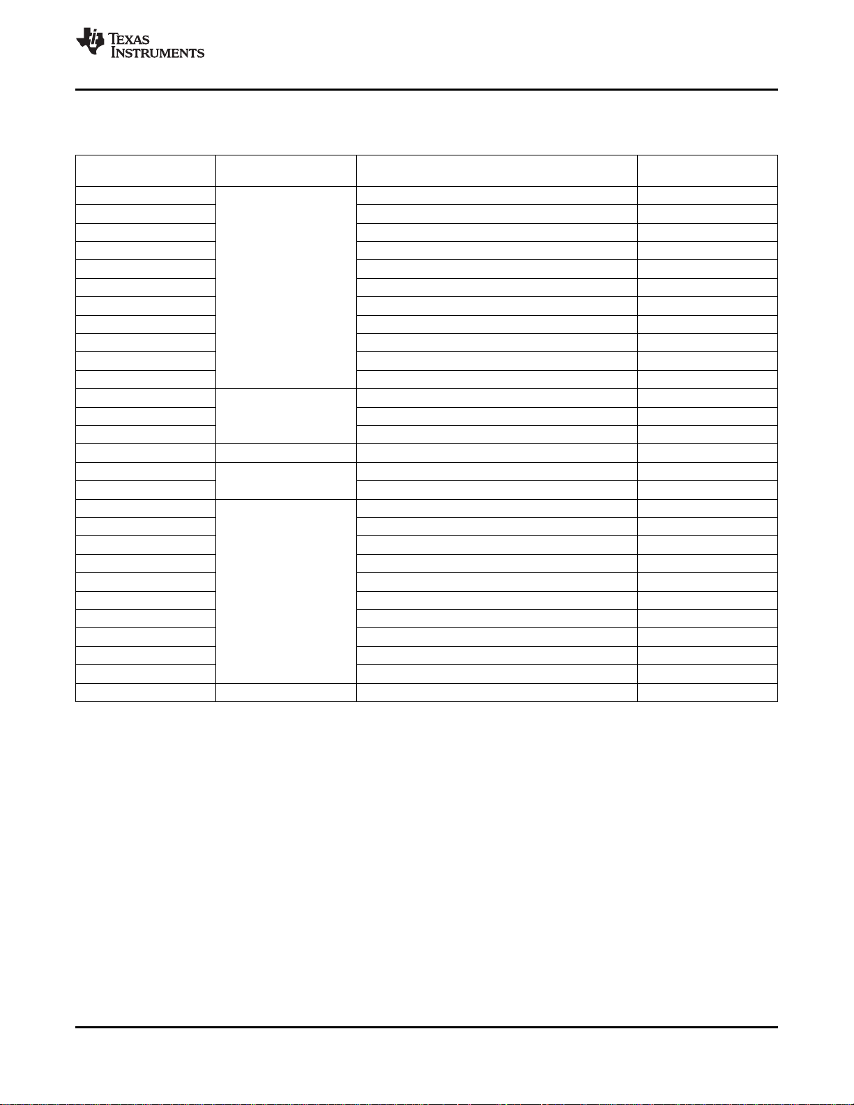
TPS40210 , TPS40211
www.ti.com
.......................................................................................................................................................... SLUS772B – MARCH 2008 – REVISED JUNE 2008
List of Materials
List of Materials
REFERENCE
DESIGNATOR
C1,C2 10 µ F, 25 V 1206
C3, C4 2.2 µ F, 100 V 1210
C5 1 nF, NPO 0603
C6 100 pF, NPO 0603
C8 100 pF 0603
C9 Capacitor 0.1 µ F 0603
C10 0.1 µ F, 25 V 0805
C11 1 µ F, 25 V 1206
C13 220 pF 0603
C14 10 nF, X7R 0603
C21 330 µ F, 25V electrolytic
D1 B2100, SHTKY, 100 V, 2 A SMB
D2 Diode BZT52C43 SOD-123
D3 MMBD7000 SOT-23
L1 Inductor Wurth 7447709100, 10 µ H, 6 A 12 × 12 × 10 mm
Q1 Si7850DP, 60 V, 31 m Ω SO-8
Q3 2N7002, 60 V, 0.1 A SOT-23
R1 15 m Ω 2512
R2 3.01 Ω 0805
R3 402 k Ω 0603
R4 14.3 k Ω 0603
R6 0.36 Ω 2512
R11 1 k Ω 0603
R13 30.1 k Ω 0603
R15 49.9 k Ω 0603
R24 10 k Ω 0603
R23 10 Ω 0603
U1 Integrated circuit TPS40211 DRC-10
MOSFET
Resistor
TYPE DESCRIPTION SIZE
Copyright © 2008, Texas Instruments Incorporated Submit Documentation Feedback 35
Product Folder Link(s): TPS40210 TPS40211

PACKAGE OPTION ADDENDUM
www.ti.com
11-Jul-2008
PACKAGING INFORMATION
Orderable Device Status
TPS40210DGQ ACTIVE MSOP-
(1)
Package
Type
Power
Package
Drawing
Pins Package
Qty
Eco Plan
DGQ 10 80 Green (RoHS &
no Sb/Br)
PAD
TPS40210DGQR ACTIVE MSOP-
Power
DGQ 10 2500 Green (RoHS &
no Sb/Br)
PAD
TPS40210DGQRG4 ACTIVE MSOP-
Power
DGQ 10 2500 Green (RoHS &
no Sb/Br)
PAD
TPS40210DRCR ACTIVE SON DRC 10 3000 Green (RoHS &
no Sb/Br)
TPS40210DRCRG4 ACTIVE SON DRC 10 3000 Green (RoHS &
no Sb/Br)
TPS40210DRCT ACTIVE SON DRC 10 250 Green (RoHS &
no Sb/Br)
TPS40211DGQ ACTIVE MSOP-
Power
DGQ 10 80 Green (RoHS &
no Sb/Br)
PAD
TPS40211DGQR ACTIVE MSOP-
Power
DGQ 10 2500 Green (RoHS &
no Sb/Br)
PAD
TPS40211DGQRG4 ACTIVE MSOP-
Power
DGQ 10 2500 Green (RoHS &
no Sb/Br)
PAD
TPS40211DRCR ACTIVE SON DRC 10 3000 Green (RoHS &
no Sb/Br)
TPS40211DRCRG4 ACTIVE SON DRC 10 3000 Green (RoHS &
no Sb/Br)
TPS40211DRCT ACTIVE SON DRC 10 250 Green (RoHS &
no Sb/Br)
(1)
The marketing status values are defined as follows:
ACTIVE: Product device recommended for new designs.
LIFEBUY: TI has announced that the device will be discontinued, and a lifetime-buy period is in effect.
NRND: Not recommended for new designs. Device is in production to support existing customers, but TI does not recommend using this part in
a new design.
PREVIEW: Device has been announced but is not in production. Samples may or may not be available.
OBSOLETE: TI has discontinued the production of the device.
(2)
Lead/Ball Finish MSL Peak Temp
CU NIPDAU Level-1-260C-UNLIM
CU NIPDAU Level-1-260C-UNLIM
CU NIPDAU Level-1-260C-UNLIM
CU NIPDAU Level-2-260C-1 YEAR
CU NIPDAU Level-2-260C-1 YEAR
CU NIPDAU Level-2-260C-1 YEAR
CU NIPDAU Level-1-260C-UNLIM
CU NIPDAU Level-1-260C-UNLIM
CU NIPDAU Level-1-260C-UNLIM
CU NIPDAU Level-2-260C-1 YEAR
CU NIPDAU Level-2-260C-1 YEAR
CU NIPDAU Level-2-260C-1 YEAR
(3)
(2)
Eco Plan - The planned eco-friendly classification: Pb-Free (RoHS), Pb-Free (RoHS Exempt), or Green (RoHS & no Sb/Br) - please check
http://www.ti.com/productcontent for the latest availability information and additional product content details.
TBD: The Pb-Free/Green conversion plan has not been defined.
Pb-Free (RoHS): TI's terms "Lead-Free" or "Pb-Free" mean semiconductor products that are compatible with the current RoHS requirements
for all 6 substances, including the requirement that lead not exceed 0.1% by weight in homogeneous materials. Where designed to be soldered
at high temperatures, TI Pb-Free products are suitable for use in specified lead-free processes.
Pb-Free (RoHS Exempt): This component has a RoHS exemption for either 1) lead-based flip-chip solder bumps used between the die and
package, or 2) lead-based die adhesive used between the die and leadframe. The component is otherwise considered Pb-Free (RoHS
compatible) as defined above.
Green (RoHS & no Sb/Br): TI defines "Green" to mean Pb-Free (RoHS compatible), and free of Bromine (Br) and Antimony (Sb) based flame
retardants (Br or Sb do not exceed 0.1% by weight in homogeneous material)
(3)
MSL, Peak Temp. -- The Moisture Sensitivity Level rating according to the JEDEC industry standard classifications, and peak solder
temperature.
Addendum-Page 1

PACKAGE OPTION ADDENDUM
www.ti.com
Important Information and Disclaimer:The information provided on this page represents TI's knowledge and belief as of the date that it is
provided. TI bases its knowledge and belief on information provided by third parties, and makes no representation or warranty as to the
accuracy of such information. Efforts are underway to better integrate information from third parties. TI has taken and continues to take
reasonable steps to provide representative and accurate information but may not have conducted destructive testing or chemical analysis on
incoming materials and chemicals. TI and TI suppliers consider certain information to be proprietary, and thus CAS numbers and other limited
information may not be available for release.
In no event shall TI's liability arising out of such information exceed the total purchase price of the TI part(s) at issue in this document sold by TI
to Customer on an annual basis.
11-Jul-2008
Addendum-Page 2

PACKAGE MATERIALS INFORMATION
www.ti.com
TAPE AND REEL INFORMATION
5-Sep-2008
*All dimensions are nominal
Device Package
Type
TPS40210DRCR SON DRC 10 3000 330.0 12.4 3.3 3.3 1.1 8.0 12.0 Q2
TPS40210DRCT SON DRC 10 250 180.0 12.4 3.3 3.3 1.1 8.0 12.0 Q2
TPS40211DRCR SON DRC 10 3000 330.0 12.4 3.3 3.3 1.1 8.0 12.0 Q2
TPS40211DRCT SON DRC 10 250 180.0 12.4 3.3 3.3 1.1 8.0 12.0 Q2
Package
Drawing
Pins SPQ Reel
Diameter
(mm)
Reel
Width
W1 (mm)
A0 (mm) B0 (mm) K0 (mm) P1
(mm)W(mm)
Pin1
Quadrant
Pack Materials-Page 1

PACKAGE MATERIALS INFORMATION
www.ti.com
5-Sep-2008
*All dimensions are nominal
Device Package Type Package Drawing Pins SPQ Length (mm) Width (mm) Height (mm)
TPS40210DRCR SON DRC 10 3000 346.0 346.0 29.0
TPS40210DRCT SON DRC 10 250 190.5 212.7 31.8
TPS40211DRCR SON DRC 10 3000 346.0 346.0 29.0
TPS40211DRCT SON DRC 10 250 190.5 212.7 31.8
Pack Materials-Page 2
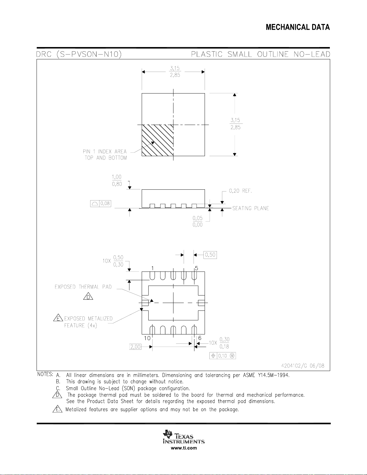


IMPORTANT NOTICE
Texas Instruments Incorporated and its subsidiaries (TI) reserve the right to make corrections, modifications, enhancements, improvements,
and other changes to its products and services at any time and to discontinue any product or service without notice. Customers should
obtain the latest relevant information before placing orders and should verify that such information is current and complete. All products are
sold subject to TI’s terms and conditions of sale supplied at the time of order acknowledgment.
TI warrants performance of its hardware products to the specifications applicable at the time of sale in accordance with TI’s standard
warranty. Testing and other quality control techniques are used to the extent TI deems necessary to support this warranty. Except where
mandated by government requirements, testing of all parameters of each product is not necessarily performed.
TI assumes no liability for applications assistance or customer product design. Customers are responsible for their products and
applications using TI components. To minimize the risks associated with customer products and applications, customers should provide
adequate design and operating safeguards.
TI does not warrant or represent that any license, either express or implied, is granted under any TI patent right, copyright, mask work right,
or other TI intellectual property right relating to any combination, machine, or process in which TI products or services are used. Information
published by TI regarding third-party products or services does not constitute a license from TI to use such products or services or a
warranty or endorsement thereof. Use of such information may require a license from a third party under the patents or other intellectual
property of the third party, or a license from TI under the patents or other intellectual property of TI.
Reproduction of TI information in TI data books or data sheets is permissible only if reproduction is without alteration and is accompanied
by all associated warranties, conditions, limitations, and notices. Reproduction of this information with alteration is an unfair and deceptive
business practice. TI is not responsible or liable for such altered documentation. Information of third parties may be subject to additional
restrictions.
Resale of TI products or services with statements different from or beyond the parameters stated by TI for that product or service voids all
express and any implied warranties for the associated TI product or service and is an unfair and deceptive business practice. TI is not
responsible or liable for any such statements.
TI products are not authorized for use in safety-critical applications (such as life support) where a failure of the TI product would reasonably
be expected to cause severe personal injury or death, unless officers of the parties have executed an agreement specifically governing
such use. Buyers represent that they have all necessary expertise in the safety and regulatory ramifications of their applications, and
acknowledge and agree that they are solely responsible for all legal, regulatory and safety-related requirements concerning their products
and any use of TI products in such safety-critical applications, notwithstanding any applications-related information or support that may be
provided by TI. Further, Buyers must fully indemnify TI and its representatives against any damages arising out of the use of TI products in
such safety-critical applications.
TI products are neither designed nor intended for use in military/aerospace applications or environments unless the TI products are
specifically designated by TI as military-grade or "enhanced plastic." Only products designated by TI as military-grade meet military
specifications. Buyers acknowledge and agree that any such use of TI products which TI has not designated as military-grade is solely at
the Buyer's risk, and that they are solely responsible for compliance with all legal and regulatory requirements in connection with such use.
TI products are neither designed nor intended for use in automotive applications or environments unless the specific TI products are
designated by TI as compliant with ISO/TS 16949 requirements. Buyers acknowledge and agree that, if they use any non-designated
products in automotive applications, TI will not be responsible for any failure to meet such requirements.
Following are URLs where you can obtain information on other Texas Instruments products and application solutions:
Products Applications
Amplifiers amplifier.ti.com Audio www.ti.com/audio
Data Converters dataconverter.ti.com Automotive www.ti.com/automotive
DSP dsp.ti.com Broadband www.ti.com/broadband
Clocks and Timers www.ti.com/clocks Digital Control www.ti.com/digitalcontrol
Interface interface.ti.com Medical www.ti.com/medical
Logic logic.ti.com Military www.ti.com/military
Power Mgmt power.ti.com Optical Networking www.ti.com/opticalnetwork
Microcontrollers microcontroller.ti.com Security www.ti.com/security
RFID www.ti-rfid.com Telephony www.ti.com/telephony
RF/IF and ZigBee® Solutions www.ti.com/lprf Video & Imaging www.ti.com/video
Mailing Address: Texas Instruments, Post Office Box 655303, Dallas, Texas 75265
Copyright © 2008, Texas Instruments Incorporated
Wireless www.ti.com/wireless
 Loading...