

Page 1

User's Guide
SLVU147A – February 2006 – Revised March 2006
Using the TPS40200
The TPS40200EVM-001 evaluation module (EVM) uses the TPS40200
nonsynchronous buck converter to provide a resistor-selected 3.3-V output voltage that
delivers up to 2.5 A from a 12-V input bus. The EVM operates from a single supply and
uses a single P-channel power FET and Schottky diode to produce a low-cost buck
converter. The part operates at a 300-kHz clock frequency with provision for external
frequency synchronization.
Contents
1 Description ........................................................................................... 2
2 TPS40200EVM-001 Electrical and Performance Specifications ............................. 2
3 Schematic ........................................................................................... 3
4 Test Setup ........................................................................................... 4
5 TPS40200EVM Typical Performance Data and Characteristic Curves ..................... 7
6 EVM Assembly Drawings and Layout ........................................................... 9
7 List of Materials .................................................................................... 14
List of Figures
1 TPS40200EVM-001 Schematic ................................................................... 3
2 TPS40200 Synchronized to a 50% Duty Cycle External Clock .............................. 4
3 TPS40200EVM-001 Recommended Test Setup ............................................... 6
4 Output Ripple Measurement - Tip and Barrel Using TP14 and TP15 ....................... 6
5 TPS40200EVM-001 Efficiency .................................................................... 7
6 TPS40200EVM-001 Efficiency .................................................................... 8
7 TPS40200EVM-001 Line and Load Regulation – Vout = 3.3255 V .......................... 8
8 TPS40200EVM-001 Line and Load Regulation – Vout = 5.0665 V ......................... 9
9 TPS40200EVM-001 Component Placement (Viewed from Top) ........................... 10
10 TPS40200EVM-001 Silkscreen (Viewed from Top) .......................................... 11
11 TPS40200EVM-001 Top View .................................................................. 12
12 TPS40200EVM-001 Bottom View ............................................................... 13
1 Adjusting V
2 TPS40200EVM-001 Bill of Materials ........................................................... 14
SLVU147A – February 2006 – Revised March 2006 Using the TPS40200 1
Submit Documentation Feedback
OUT
List of Tables
With R6 Rounded to Standard 1% Resistor Values ......................... 3
Page 2

www.ti.com
Description
1 Description
TPS40200EVM-001 is designed to operate with an 8-V to 16-V input and to produce a regulated 3.3-V
output with a load current from 0.125 A to 2.5 A. The TPS40200EVM-001 demonstrates the use of the
TPS40200 in a typical buck converter application. The board sacrifices some packing density to provide
ample test points for module evaluation. This EVM can be modified to support output voltages from 0.7 V
to 5 V by changing a single feedback resistor. The TPS40200EVM-001 has been built to the sample
application as described in the Application Information section of the TPS40200 data sheet (SLUS659 ).
1.1 Features
• 8-V to 16-V input range
• 3.3-V output, adjustable with single feedback resistor
• 0.125-A to 2.5-A steady-state output current
• 300-kHz switching frequency
• Single P-channel MOSFET and single rectifier
• Two-layer, 1.4-inch × 2.12-inch, surface-mount design with all components on one side
• Convenient test points for probing critical waveforms and noninvasive loop response testing
1.2 Applications
• Nonisolated medium-current, point-of-load and low-voltage bus converters
• Scanners
• Industrial controls
• Distributed power systems
• DSL/cable modems
2 TPS40200EVM-001 Electrical and Performance Specifications
PARAMETER TEXT CONDITIONS MIN NOM MAX UNIT
V
V
V
V
V
V
I
OUT
I
SCP
F
(1)
Input voltage 8 12 16 V
IN
Output voltage IOUT at 2.5 A, R6 = 26.7 k Ω 3.200 3.3 3.400
OUT
Line regulation ± 0.2% Vout 3.293 3.3 3.307 V
Load regulation ± 0.2% Vout 3.293 3.3 3.307 V
Output voltage IOUT at 2.5 A, R6 = 16.5 k Ω 4.85 5 5.150
OUT
Line regulation ± 0.2% Vout 4.990 5 5.010 V
Load regulation ± 0.2% Vout 4.990 5 5.010 V
Output ripple voltage At maximum output current 60 mV
RIPPLE
Output overshoot For 2.375-A load transient 60 mV
OVER
Output undershoot For 2.375-A load transient 60 mV
UNDER
Output current 0.125 2.5 A
Short-circuit current trip point Imax +50% minimum 3.75 5 A
Efficiency At nominal input voltage and maximum output 90%
Switching frequency 300 kHz
S
Set-point accuracy depends on external resistor tolerance and the reference voltage. Line and load regulation values are
referenced to the nominal design output voltage.
current
(1)
V
(1)
V
Using the TPS402002 SLVU147A – February 2006 – Revised March 2006
Submit Documentation Feedback
Page 3
www.ti.com
Notes
R6 =26.7k for 3.3 Vout, R6 = 16.2k for 5.0 Vout
+
+
D3 : Do not populate. SOT 23 Common Cathode Dual Schottky
V
vout
V
ref
1
R
10
R
6
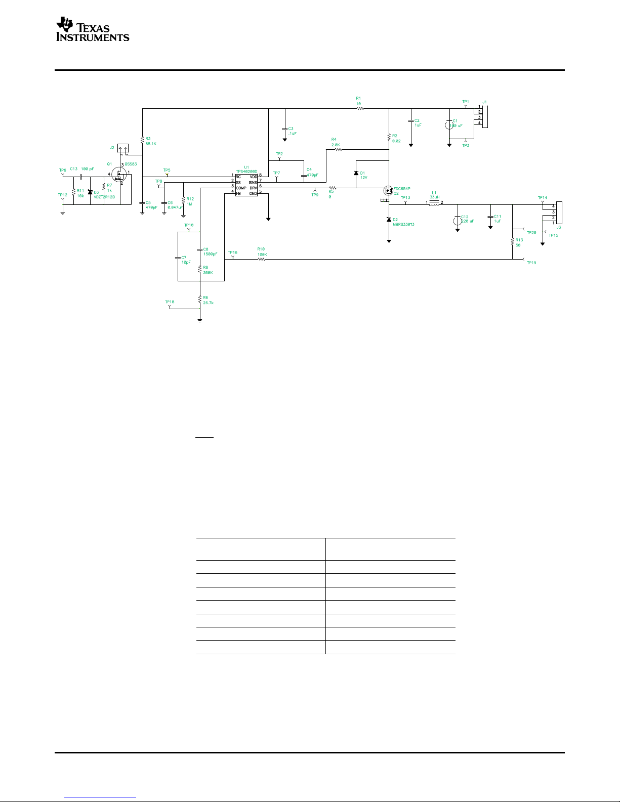
Schematic
3 Schematic
NOTE: For reference only; see Table 2, Bill of Materials for specific values
Figure 1. TPS40200EVM-001 Schematic
3.1 Adjusting Output Voltage (R6 and R10)
The regulated output voltage can be adjusted within a limited range by changing the ground resistor in the
feedback resistor divider (R6 and R10). The output voltage is given by Equation 1 .
Where V
Table 1 contains common values for R6 to generate popular output voltages. TPS40200EVM-001 is stable
through these output voltages with the efficiency rising with output voltage.
= 0.700 V and R10 = 100 k Ω
REF
V
Table 1. Adjusting V
- Output Voltage (V) R6 - Feedback Resistor Divider
OUT
With R6 Rounded to
OUT
Standard 1% Resistor Values
5 16.2
3.3 26.7
2.5 39
2 53.6
1.8 63.4
1.5 86.6
1.2 140
(1)
(k Ω )
3.2 Using Remote Synchronizing (TP6)
The TPS40200EVM-001 board has a synchronizing circuit that uses TP6 as an input. A logic high at this
input turns on a small signal FET (Q1) whose drain is connected to the oscillator setting node (RC) on the
TPS40200. The switching of this transistor over-drives the ramp associated with the internal oscillator and
causes the PWM switching to follow the input clock frequency. For reliable operation, the external clock
SLVU147A – February 2006 – Revised March 2006 Using the TPS40200 3
Submit Documentation Feedback
Page 4
www.ti.com
Test Setup
frequency should be 25% to 30% higher than the frequency set by R3 and C5. The BSS83 used in this
circuit has a low (1-pF) output capacitance; so, its presence does not load down the normal operation of
the RC pin. With the controller’s frequency set to a 300-kHz frequency, the module synchronizes to a
390-kHz external clock that has a 50% duty cycle. A shorting jack, J2, is provided to disconnect the
synchronizing circuit from the (RC) node.
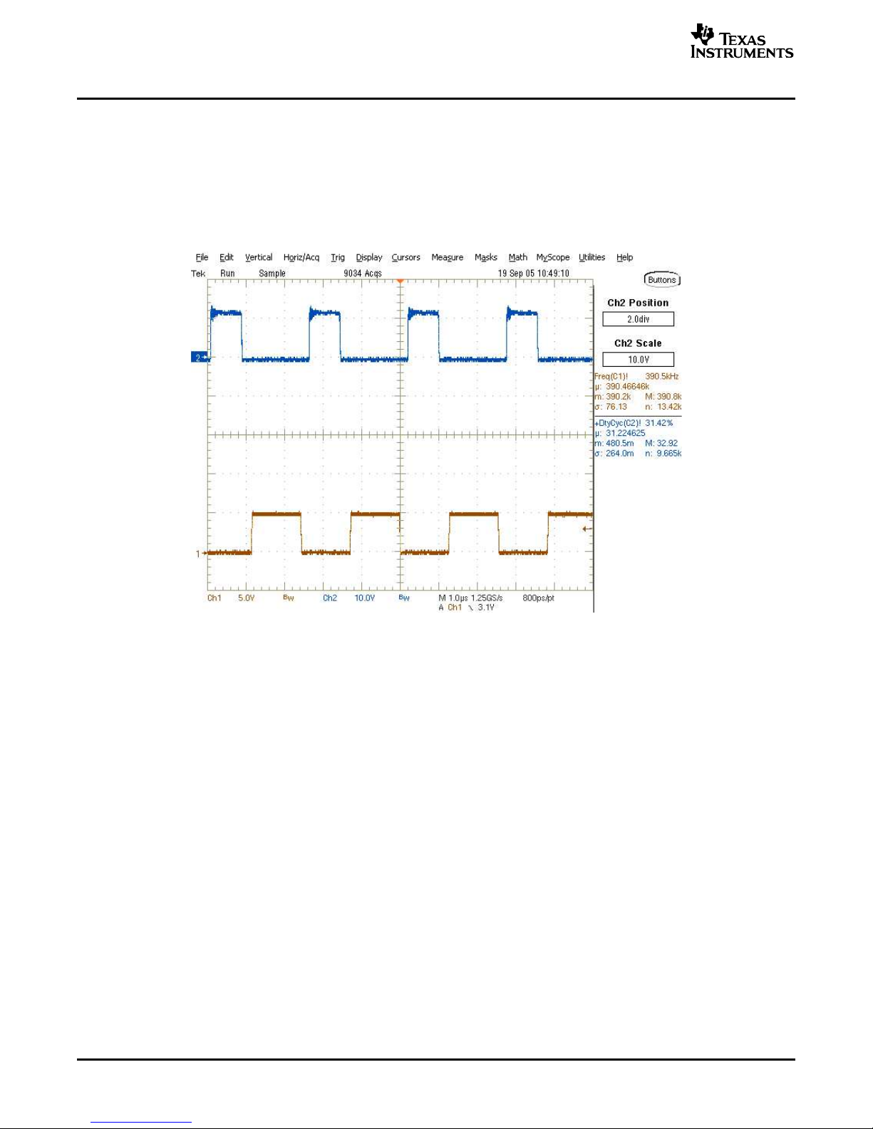
The following scope picture (Figure 2 ) shows a 5-V input clock at the TP6 input operating at 390 kHz and
a 50% duty cycle. The switch node also shown in the picture is switching at the same frequency with a
12-V V
supply. The RC operating frequency of the TPS40200 is set by R3 and C5 to be 300 kHz.
CC
Figure 2. TPS40200 Synchronized to a 50% Duty Cycle External Clock
4 Test Setup
4.1 Equipment
4.1.1 Voltage Source
V
— The input voltage source (V
12V_IN
METERS
A1: 0-A to 5-A dc ammeter
V1: V
V2: V
4.1.2 Loads
LOAD1 — The output load (LOAD1) should be an electronic constant-current-mode load capable of 0
A-to-2.5 A dc at 1.5 V.
4.1.3 Recommended Wire Gauge
V
to J1 — The connection between the source voltage, V
12V_IN
as 3 A dc. The minimum recommended wire size is AWG 16 with the length of wire less than 4 feet (2 feet
input, 2 feet return).
, 0-V to 20-V voltmeter
12V_IN
3V3_OUT
0 V to 10-V voltmeter
) should be a 0-V to 20-V variable dc source capable of 5 A dc.
12V_IN
and J1 of HPA164 can carry as much
12V_IN
4 Using the TPS40200 SLVU147A – February 2006 – Revised March 2006
Submit Documentation Feedback
Page 5

www.ti.com
J3 to LOAD1 (Power) — The power connection between J3 of HPA164 and LOAD1 can carry as much as
5 A dc. The minimum recommended wire size is 2x AWG 16, with the length of wire less than 4 feet (2
feet output, 2 feet return).
J3 to LOAD1 (Remote Sense) — If remote sense is used, the remote sense connection between J3 of
HPA164 and LOAD1 will carry less than 1 A dc. The minimum recommended wire size is AWG 22, with
the length of wire less and 4 feet (2 feet output, 2 feet return).
4.1.4 Oscilloscope
A 60-MHz or faster oscilloscope can be used to determine the ripple voltage on 3V3_OUT. The
oscilloscope should be set for 1-M Ω impedance, ac coupling, 1- µ s/division horizontal resolution,
20-mV/division vertical resolution for taking output ripple measurements. TP14 and TP15 can be used to
measure the output ripple voltage by placing the oscilloscope probe tip through TP14 and holding the
ground barrel to TP15 as shown in Figure 3 . For a hands-free approach, the loop in TP15 can be cut and
opened to cradle the probe barrel. Using a leaded ground connection may induce additional noise due to
the large ground loop area. Connect a short wire from the barrel of the scope probe to TP15 as necessary
to reach between TP14 and TP15.
4.2 Equipment Setup
Shown in Figure 3 is the basic test setup recommended to evaluate the TPS40200EVM-001. Note that
although the return for J1 and J3 are the same, the connections should remain separate as shown in
Figure 3 .
4.2.1 Procedure
1. Working at an ESD workstation, ensure that any wrist straps, bootstraps, or mats are connected
referencing the user to earth ground before power is applied to the EVM. Electrostatic smock and
safety glasses should also be worn.
2. Prior to connecting the dc-input source, V
5 A maximum. Ensure that V
3. Connect the ammeter A1 (0-A to 5-A range) between V
4. Connect voltmeter V1 to TP1 and TP3 as shown in Figure 3 .
5. Connect LOAD1 to J3 as shown in Figure 1 . Set LOAD1 to constant current mode to sink 0 A dc
before V
6. Connect voltmeter, V2 across J3 pin 3 and J3 pin 2 as shown in Figure 3 .
7. Connect the oscilloscope probe to TP14 and TP15 as shown in Figure 4 .
Test Setup
, it is advisable to limit the source current from V
12V_IN
is initially set to 0 V and connected as shown in Figure 2 .
12V_IN
and J1 as shown in Figure 3 .
12V_IN
is applied.
12V_IN
to
12V_IN
SLVU147A – February 2006 – Revised March 2006 Using the TPS40200 5
Submit Documentation Feedback
Page 6

www.ti.com
LOAD1
3.3V @
2.5A
−
+
V1
−3V3_OUT +
+12V_IN −
+−
Oscilloscope
1M , AC
20mV / div
20MHz
+
A1
V
−
+
12V_IN
TP1
TP3
TP 14
TP6
TEXAS INSTRUMENTS
TPS40200EVM−001
12V to 3.3V @ 2.5A with sync Input
HPA164
J1
+
−
Sync
See Tip and Barrel
Measurement for V out
ripple
J2
Short
for
Sync
−
+
J1
+
−
TP1
−
+
+
TP1
J1
J3
+
V2
TP 15
+
−
TP15TP14
Metal Ground Barrel
Probe Tip
Tip and Barrel Vout ripple measurement
Test Setup
4.2.2 Diagram
4.3 Startup/Shutdown Procedure
Figure 3. TPS40200EVM-001 Recommended Test Setup
Figure 4. Output Ripple Measurement - Tip and Barrel Using TP14 and TP15
1. Increase V
2. Vary LOAD1 from 0 A to 2.5 A dc.
3. Vary V
12V_IN
(V1) from 0 V to 12 V dc.
12V_IN
(V1) from 8 Vdc to 16 V dc.
4. Decrease LOAD1 to 0 A.
5. Decrease V12V_IN to 0 V.
Using the TPS402006 SLVU147A – February 2006 – Revised March 2006
Submit Documentation Feedback
Page 7

www.ti.com
0
10
20
30
40
50
60
70
80
90
100
0
0.5
1
1.5
2
2.5
3
VI= 8 V
VI= 12 V
VI= 16 V
VO= 3.3 V
− Efficiency − %
IO− Load Current − A
TPS40200EVM Typical Performance Data and Characteristic Curves
4.4 Equipment Shutdown
1. Shut down oscilloscope.
2. Shut down LOAD1.
3. Shut down V
.
12V_IN
5 TPS40200EVM Typical Performance Data and Characteristic Curves
Figure 5 through Figure 8 present typical performance curves for the TPS40200EVM-001. Because actual
performance data can be affected by measurement techniques and environmental variables, these curves
are presented for reference and may differ from actual field measurements.
5.1 Efficiency
NOTE: V
= 8-, 12-, and 16-V, V
12V_IN
= 3.3 V, I
3V3_OUT
1V5_OUT
= 0.125 A to 2.5 A
Figure 5. TPS40200EVM-001 Efficiency
SLVU147A – February 2006 – Revised March 2006 Using the TPS40200 7
Submit Documentation Feedback
Page 8

www.ti.com
0
10
20
30
40
50
60
70
80
90
100
0
0.5
1
1.5
2
2.5
3
VI= 8 V
VO= 5 V
− Efficiency − %
IO− Load Current − A
VI= 12 V
VI= 16 V
3.322
3.323
3.324
3.325
3.326
3.327
3.328
3.329
3.33
3.331
0
0.5
1
1.5
2
2.5
3
VI = 8 V
IO − Load Current − A
VI = 12 V
VI = 16 V
− Output Voltage − V
V
O
VO = 3.3255 V
TPS40200EVM Typical Performance Data and Characteristic Curves
NOTE: V
= 8-, 12-, and 16-V, V
12V_IN
5.2 Line and Load Regulation
8 Using the TPS40200 SLVU147A – February 2006 – Revised March 2006
Figure 7. TPS40200EVM-001 Line and Load Regulation – Vout = 3.3255 V
= 5 V, I
3V3_OUT
Figure 6. TPS40200EVM-001 Efficiency
1V5_OUT
= 0.125 A to 2.5 A
Submit Documentation Feedback
Page 9

www.ti.com
5.062
5.064
5.066
5.068
5.07
5.072
5.074
5.076
0 0.5 1 1.5 2 2.5 3
VI = 8 V
IO − Load Current − A
VI = 12 V
VI = 16 V
− Output Voltage − V
V
O
EVM Assembly Drawings and Layout
Figure 8. TPS40200EVM-001 Line and Load Regulation – Vout = 5.0665 V
6 EVM Assembly Drawings and Layout
The following figures (Figure 9 through Figure 12 ) show the design of the TPS40200EVM-001
printed-circuit board. The EVM has been designed using a 2-layer, 2-oz copper-clad circuit board, 1.4-inch
× 2.12-inch in size, with all components on the top side to allow the user to easily view, probe, and
evaluate the TPS40200 control IC in a practical application. Moving components to both sides of the PCB
or using additional internal layers can offer additional size reduction for space-constrained systems.
SLVU147A – February 2006 – Revised March 2006 Using the TPS40200 9
Submit Documentation Feedback
Page 10

www.ti.com
EVM Assembly Drawings and Layout
Figure 9. TPS40200EVM-001 Component Placement (Viewed from Top)
10 Using the TPS40200 SLVU147A – February 2006 – Revised March 2006
Submit Documentation Feedback
Page 11

www.ti.com
EVM Assembly Drawings and Layout
Figure 10. TPS40200EVM-001 Silkscreen (Viewed from Top)
SLVU147A – February 2006 – Revised March 2006 Using the TPS40200 11
Submit Documentation Feedback
Page 12

www.ti.com
EVM Assembly Drawings and Layout
Figure 11. TPS40200EVM-001 Top View
12 Using the TPS40200 SLVU147A – February 2006 – Revised March 2006
Submit Documentation Feedback
Page 13

www.ti.com
EVM Assembly Drawings and Layout
Figure 12. TPS40200EVM-001 Bottom View
SLVU147A – February 2006 – Revised March 2006 Using the TPS40200 13
Submit Documentation Feedback
Page 14

www.ti.com
List of Materials
7 List of Materials
Table 2 lists the EVM components as configured according to the schematic shown in Figure 1 .
Table 2. TPS40200EVM-001 Bill of Materials
Count Ref Value Description Size Part Number MFR
Des
1 C1 100 µ F Capacitor, Aluminum, SM, 25-V, 0.3- Ω 8 x 10 mm 20SVP100M Sanyo
2 C2, 1 µ F Capacitor, Ceramic, 50-V, X7R, 20% 603 Std Murata
C11
1 C3 0.1 µ F Capacitor, Ceramic, 50-V, X7R, 20% 603 Std Murata
2 C4, C5 470 pF Capacitor, Ceramic, 50-V, X7R, 20% 603 Std Murata
1 C6 0.047 µ F Capacitor, Ceramic, 50-V, X7R, 20% 603 Std Murata
1 C7 10 pF Capacitor, Ceramic, 50-V, COG, 20% 603 Std Murata
1 C8 1500 pF Capacitor, Ceramic, 50-V, X7R, 20% 603 Std Murata
1 C12 220 µ F Capacitor, Aluminum, SM, 6.3-V, 0.4- Ω 8 x 6,2 mm EEVFC0J221P Panasonic
1 C13 100 pF Capacitor, Ceramic, 50-V, COG, 20% 603 Std Murata
1 D1 12 V Diode, Zener, 12-V, 350-mW SOT-23 BZX84C12T Diodes, Inc.
1 D2 MBRS330T3 Diode, Schottky, 3-A, 30-V SMC MBRS330T3 On Semi
1 D3 12-V Diode, Zener, 12-V, 5-mA VMD2 VDZT2R12B Rohm
2 J1, J3 Terminal Block, 4-pin, 15-A, 5,1-mm 0.80 x 0.35 ED2227 OST
1 J2 PTC36SAAN Header, 2-pin, 100-mil spacing (36-pin strip) 0.100 x 2 PTC36SAAN Sullins
1 L1 33 µ H Inductor, SMT, 3.2-A, 0.039- Ω 12,5 x 12,5 mm SLF12575T330M3R2PF TDK
1 PCB 2 Layer PCB 2-Ounce Cu 1.4 x 2.12 x 0.062 HPA164 Any
1 Q1 BSS83 Transistor, N-ch , 50-mA SOT-143B BSS83 Philips
1 Q2 FDC654P Transistor, MOSFET, P-ch, –3.6-A, –30V, SuperSOT-6 FDC654P Fairchild
0.075- Ω
1 R1 10 Resistor, Chip, 1/16-W, 1% 603 Std Std
1 R2 0.02 Resistor, Chip, 1/2-W, 5% 2010 Std Std
1 R3 68.1k Resistor, Chip, 1/16-W, 1% 603 Std Std
1 R4 2k Resistor, Chip, 1/16-W, 1% 603 Std Std
1 R5 0 Resistor, Chip, 1/16-W, 1% 603 Std Std
1 R6 26.7k Resistor, Chip, 1/16-W, 1% 603 Std Std
1 R7 1k Resistor, Chip, 1/16-W, 1% 603 Std Std
1 R8 300k Resistor, Chip, 1/16-W, 1% 603 Std Std
1 R10 100k Resistor, Chip, 1/16-W, 1% 603 Std Std
1 R11 10k Resistor, Chip, 1/16-W, 1% 603 Std Std
1 R12 1M Resistor, Chip, 1/16-W, 1% 603 Std Std
1 R13 49.9 Resistor, Chip, 1/16-W, 1% 603 Std Std
5 TP1, 5002 Test Point, White, Thru Hole Color Keyed 0.1 x 0.1 in. 5002 Keystone
TP3,
TP13,
TP14,
TP15
12 TP2, Std Test Point, 0.020 Hole 0.1 x 0.1 in. NA NA
TP5,
TP6,
TP7,
TP8,
TP9,
TP10,
TP12,
TP16,
TP18,
TP19,
TP20
1 U1 TPS40200D IC, Low-Cost Sync Buck Controller SO-8 TPS40200D TI
Using the TPS4020014 SLVU147A – February 2006 – Revised March 2006
Submit Documentation Feedback
Page 15

EVALUATION BOARD/KIT IMPORTANT NOTICE
Texas Instruments (TI) provides the enclosed product(s) under the following conditions:
This evaluation board/kit is intended for use for ENGINEERING DEVELOPMENT, DEMONSTRATION, OR EVALUATION
PURPOSES ONLY and is not considered by TI to be a finished end-product fit for general consumer use. Persons handling the
product(s) must have electronics training and observe good engineering practice standards. As such, the goods being provided are
not intended to be complete in terms of required design-, marketing-, and/or manufacturing-related protective considerations,
including product safety and environmental measures typically found in end products that incorporate such semiconductor
components or circuit boards. This evaluation board/kit does not fall within the scope of the European Union directives regarding
electromagnetic compatibility, restricted substances (RoHS), recycling (WEEE), FCC, CE or UL, and therefore may not meet the
technical requirements of these directives or other related directives.
Should this evaluation board/kit not meet the specifications indicated in the User’s Guide, the board/kit may be returned within 30
days from the date of delivery for a full refund. THE FOREGOING WARRANTY IS THE EXCLUSIVE WARRANTY MADE BY
SELLER TO BUYER AND IS IN LIEU OF ALL OTHER WARRANTIES, EXPRESSED, IMPLIED, OR STATUTORY, INCLUDING
ANY WARRANTY OF MERCHANTABILITY OR FITNESS FOR ANY PARTICULAR PURPOSE.
The user assumes all responsibility and liability for proper and safe handling of the goods. Further, the user indemnifies TI from all
claims arising from the handling or use of the goods. Due to the open construction of the product, it is the user’s responsibility to
take any and all appropriate precautions with regard to electrostatic discharge.
EXCEPT TO THE EXTENT OF THE INDEMNITY SET FORTH ABOVE, NEITHER PARTY SHALL BE LIABLE TO THE OTHER
FOR ANY INDIRECT, SPECIAL, INCIDENTAL, OR CONSEQUENTIAL DAMAGES.
TI currently deals with a variety of customers for products, and therefore our arrangement with the user is not exclusive.
TI assumes no liability for applications assistance, customer product design, software performance, or infringement of
patents or services described herein.
Please read the User’s Guide and, specifically, the Warnings and Restrictions notice in the User’s Guide prior to handling the
product. This notice contains important safety information about temperatures and voltages. For additional information on TI’s
environmental and/or safety programs, please contact the TI application engineer or visit www.ti.com/esh .
No license is granted under any patent right or other intellectual property right of TI covering or relating to any machine, process, or
combination in which such TI products or services might be or are used.
FCC Warning
This evaluation board/kit is intended for use for ENGINEERING DEVELOPMENT, DEMONSTRATION, OR EVALUATION
PURPOSES ONLY and is not considered by TI to be a finished end-product fit for general consumer use. It generates, uses, and
can radiate radio frequency energy and has not been tested for compliance with the limits of computing devices pursuant to part 15
of FCC rules, which are designed to provide reasonable protection against radio frequency interference. Operation of this
equipment in other environments may cause interference with radio communications, in which case the user at his own expense
will be required to take whatever measures may be required to correct this interference.
EVM WARNINGS AND RESTRICTIONS
It is important to operate this EVM within the input voltage range of 0 V to 25 V and the output voltage range of 0 V to 6.3 V.
Exceeding the specified input range may cause unexpected operation and/or irreversible damage to the EVM. If there are
questions concerning the input range, please contact a TI field representative prior to connecting the input power.
Applying loads outside of the specified output range may result in unintended operation and/or possible permanent damage to the
EVM. Please consult the EVM User's Guide prior to connecting any load to the EVM output. If there is uncertainty as to the load
specification, please contact a TI field representative.
During normal operation, some circuit components may have case temperatures greater than 100 ° C. The EVM is designed to
operate properly with certain components above 100 ° C as long as the input and output ranges are maintained. These components
include but are not limited to linear regulators, switching transistors, pass transistors, and current sense resistors. These types of
devices can be identified using the EVM schematic located in the EVM User's Guide. When placing measurement probes near
these devices during operation, please be aware that these devices may be very warm to the touch.
Mailing Address: Texas Instruments, Post Office Box 655303, Dallas, Texas 75265
Copyright © 2006, Texas Instruments Incorporated
Page 16

IMPORTANT NOTICE
Texas Instruments Incorporated and its subsidiaries (TI) reserve the right to make corrections, modifications,
enhancements, improvements, and other changes to its products and services at any time and to discontinue
any product or service without notice. Customers should obtain the latest relevant information before placing
orders and should verify that such information is current and complete. All products are sold subject to TI’s terms
and conditions of sale supplied at the time of order acknowledgment.
TI warrants performance of its hardware products to the specifications applicable at the time of sale in
accordance with TI’s standard warranty. Testing and other quality control techniques are used to the extent TI
deems necessary to support this warranty. Except where mandated by government requirements, testing of all
parameters of each product is not necessarily performed.
TI assumes no liability for applications assistance or customer product design. Customers are responsible for
their products and applications using TI components. To minimize the risks associated with customer products
and applications, customers should provide adequate design and operating safeguards.
TI does not warrant or represent that any license, either express or implied, is granted under any TI patent right,
copyright, mask work right, or other TI intellectual property right relating to any combination, machine, or process
in which TI products or services are used. Information published by TI regarding third-party products or services
does not constitute a license from TI to use such products or services or a warranty or endorsement thereof.
Use of such information may require a license from a third party under the patents or other intellectual property
of the third party, or a license from TI under the patents or other intellectual property of TI.
Reproduction of information in TI data books or data sheets is permissible only if reproduction is without
alteration and is accompanied by all associated warranties, conditions, limitations, and notices. Reproduction
of this information with alteration is an unfair and deceptive business practice. TI is not responsible or liable for
such altered documentation.
Resale of TI products or services with statements different from or beyond the parameters stated by TI for that
product or service voids all express and any implied warranties for the associated TI product or service and
is an unfair and deceptive business practice. TI is not responsible or liable for any such statements.
Following are URLs where you can obtain information on other Texas Instruments products and application
solutions:
Products Applications
Amplifiers amplifier.ti.com Audio www.ti.com/audio
Data Converters dataconverter.ti.com Automotive www.ti.com/automotive
DSP dsp.ti.com Broadband www.ti.com/broadband
Interface interface.ti.com Digital Control www.ti.com/digitalcontrol
Logic logic.ti.com Military www.ti.com/military
Power Mgmt power.ti.com Optical Networking www.ti.com/opticalnetwork
Microcontrollers microcontroller.ti.com Security www.ti.com/security
Telephony www.ti.com/telephony
Video & Imaging www.ti.com/video
Wireless www.ti.com/wireless
Mailing Address: Texas Instruments
Post Office Box 655303 Dallas, Texas 75265
Copyright 2006, Texas Instruments Incorporated
 Loading...