www.ti.com
1
2
3
4
EN
FB
COMP
VDD
TPS40195
5
6
7
8
ULVO
RT
ILIM
GND
16
15
14
13
HDRV
SW
BOOT
LDRV
12
11
10
9
BP
SS_SEL
PGOOD
SYNC
Power Good
V
OUT
UDG-06066
SLUS720 – FEBRUARY 2007
4.5-V TO 20-V SYNCHRONOUS BUCK CONTROLLER WITH SYNCHRONIZATION AND
POWER GOOD
FEATURES CONTENTS
• Input Operating Voltage Range: 4.5 V to 20 V
• Output Voltage as Low as 0.591 V ± 0.5%
• 180 ° Bi-Directional Out-of-Phase
Synchronization
• Internal 5-V Regulator
• High and Low MOSFET Sense Overcurrent Design Example 20
• 100 kHz to 600 kHz Switching Frequency
• Enable and Power Good
• Programmable UVLO and Hysteresis
• Thermal Shutdown at 150 ° C
• Selectable Soft-Start
• Pre-Bias Output Safe
APPLICATIONS
• Digital TV
• Entry-Level and Midrange Servers
• Networking Equipment
• Non-Isolated DC-DC modules
Device Ratings 2
Electrical Characteristics 3
Typical Characteristics 5
Terminal Information 9
Application Information 11
Additional References 33
DESCRIPTION
The TPS40195 is a flexible synchronous buck
controller that operates from a nominal 4.5 V to 20 V
supply. This controller implements voltage mode
control with the switching frequency adjustable from
100 kHz to 600 kHz. Flexible features found on this
device include selectable soft-start time,
programmable short circuit limit, programmable
undervoltage lockout (UVLO) and synchronization
capability. An adaptive anti-cross conduction scheme
is used to prevent shoot through current in the power
FETs. Short-circuit detection is done by sensing the
voltage drop across the low-side MOSFET when it is
on, and comparing it with a user programmable
threshold.
TPS40195
Please be aware that an important notice concerning availability, standard warranty, and use in critical applications of Texas
Instruments semiconductor products and disclaimers thereto appears at the end of this data sheet.
PRODUCTION DATA information is current as of publication date.
Products conform to specifications per the terms of the Texas
Instruments standard warranty. Production processing does not
necessarily include testing of all parameters.
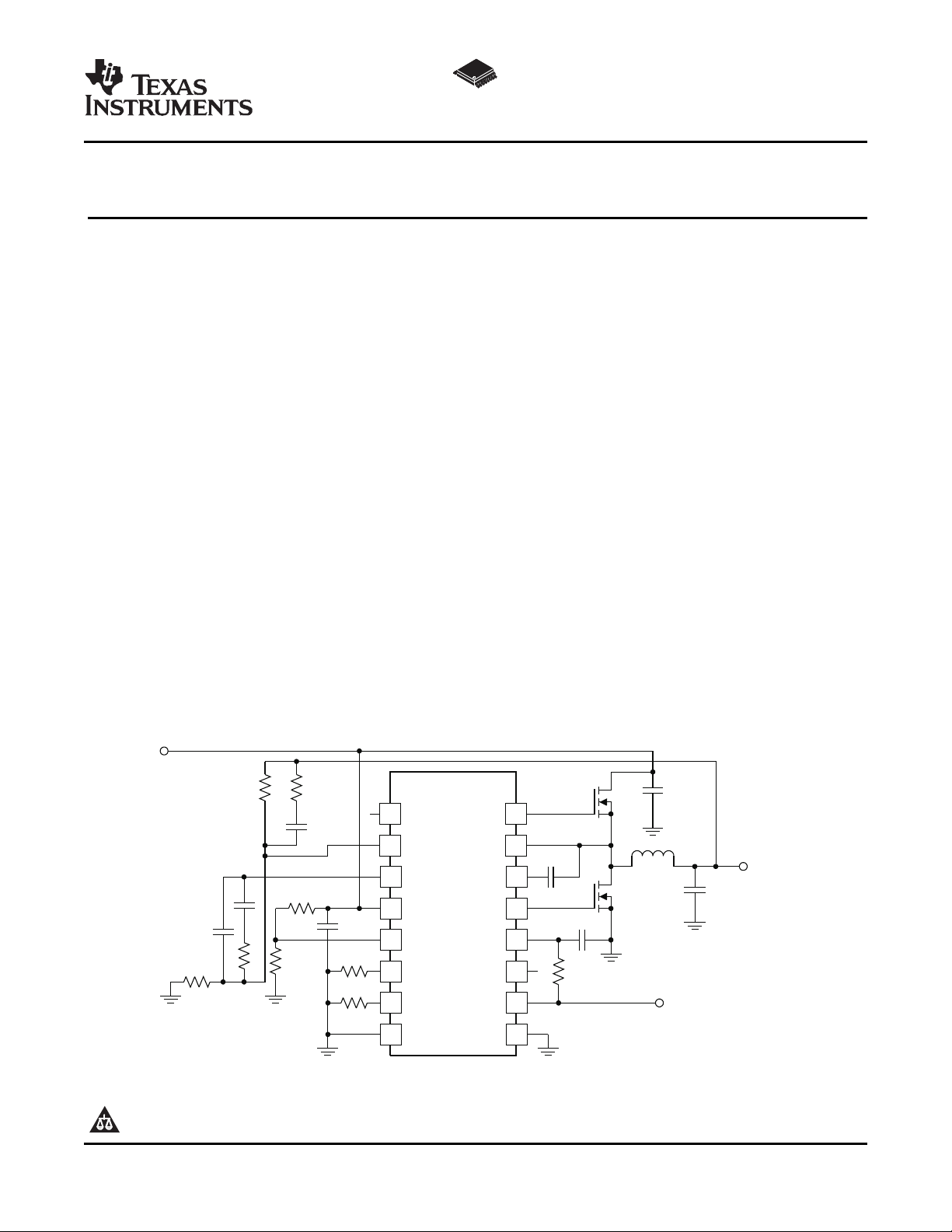
SIMPLIFIED APPLICATION DIAGRAM
Copyright © 2007, Texas Instruments Incorporated

www.ti.com
TPS40195
SLUS720 – FEBRUARY 2007
These devices have limited built-in ESD protection. The leads should be shorted together or the device placed in conductive foam
during storage or handling to prevent electrostatic damage to the MOS gates.
DESCRIPTION (CONTINUED)
The threshold is set with a single external resistor connected from ILIM to GND. Pulse-by-pulse limiting (to
prevent current runaway) is provided by sensing the voltage across the high-side MOSFET when it is on and
terminating the cycle when the voltage drop rises above a fixed threshold of 550 mV. When the controller
senses an output short circuit, both MOSFETs are turned off and a timeout period is observed before attempting
to restart. This provides limited power dissipation in the event of a sustained fault. Synchronization on this
device is bi-directional. Devices can be synchronized 180 ° out of phase to a chosen master TPS40195 running
at a fixed 250 kHz or 500 kHz, or can be synchronized to an outside clock source anywhere in the 100 kHz to
600 kHz range.
ORDERING INFORMATION
T
J
-40 ° C to 85 ° C
(1) For the most current package and ordering information, see the Package Option Addendum at the end of this document, or see the TI
Web site at www.ti.com .
PACKAGE QUANTITY PACKAGING
Plastic 16-Pin TSSOP
(PW)
90 Tube TPS40195PW
2000 Reel TPS40195PWR
(1)
PART NUMBER
DEVICE RATINGS
ABSOLUTE MAXIMUM RATINGS
over operating free-air temperature range unless otherwise noted
VDD –0.3 to 22
SW –5 to 25
BOOT –0.3 to 30
Input voltage range HDRV -5 to 30 V
BOOT–SW, HDRV–SW (Differential from BOOT or HDRV to SW) –0.3 to 6
EN, FB, BP, LDRV, PGOOD, ILIM, SYNC, UVLO, SS_SEL, RT –0.3 to 6
COMP –0.3 to 3
T
Operating junction temperature range –40 to 150
J
T
Storage temperature –55 to 150
stg
(1) Stresses beyond those listed under "absolute maximum ratings" may cause permanent damage to the device. These are stress ratings
only, and functional operation of the device at these or any other conditions beyond those indicated under "recommended operating
conditions" is not implied. Exposure to absolute-maximum-rated conditions for extended periods may affect device reliability.
(1)
TPS40195 UNIT
RECOMMENDED OPERATING CONDITIONS
MIN NOM MAX UNIT
V
Input voltage 4.5 20 V
VDD
T
Operating junction temperature -40 125 ° C
J
° C
PACKAGE DISSIPATION RATINGS
R
High-K Board
PACKAGE AIRFLOW (LFM)
PW 0 (Natural Convection) 110 0.90 0.36
(1) Ratings based on JEDEC High Thermal Conductivity (High K) Board. For more information on the test method, see TI Technical Brief
SZZA017 .
2
θ JA
Submit Documentation Feedback
( ° C/W) TA= 25 ° C TA= 85 ° C
(1)
Power Rating (W) Power Rating (W)

www.ti.com
ELECTROSTATIC DISCHARGE (ESD) PROTECTION
Human Body Model (HBM) 2500
Charged Device Model (CDM) 1500
ELECTRICAL CHARACTERISTICS
TJ= –40 ° C to 85 ° C, V
REFERENCE
V
FB
INPUT SUPPLY
V
VDD
I
VDD
ON BOARD REGULATOR
V
BP
V
DO
I
SC
I
BP
OSCILLATOR
f
SW
V
RMP
SYNCHRONIZATION
V
INH
V
INL
T
F(max)
V
OH
V
OL
T
F
T
R
PWM
D
MAX
t
ON(min)
t
DEAD
SOFT-START
t
SS
(1) Specified by design. Not production tested.
Feedback voltage range mV
Input voltage range 4.5 20.0 V
Operating current V
Output voltage V
Regulator dropout voltage, V
Regulator current limit threshold 75
Average current 75
Switching frequency V
Ramp amplitude
High-level input voltage 2.5
Low-level input voltage 0.5
Maximum input fall time
High-level output voltage I
Low-level output voltage I
Output rise time
Output fall time
Maximum duty cycle
Minimum controlled pulse
Output driver dead time
Soft-start time ms
= 12 Vdc, all parameters at zero power dissipation (unless otherwise noted)
VDD
PARAMETER TEST CONDITIONS MIN TYP MAX UNIT
0 ° C ≤ TJ≤ 85 ° C 588 591 594
-40 ° C ≤ TJ≤ 85 ° C 585 591 594
V
= 3 V 4 mA
EN
< 0.6 V, V
EN
V
< 0.6 V, V
EN
> 6 V, IBP≤ 10 mA 5.1 5.3 5.5 V
VDD
- V
VDD
(1)
(1)
(1)
(1)
(1)
(1)
V
BP
= 5 V, IBP≤ 25 mA 350 550 mV
VDD
V
= V
RT
BP
= 0 V 200 250 290 kHz
RT
R
= 100 k Ω 250
RT
= 100 µ A, sourcing 3.5
SYNC
= 100 µ A, sinking 0.3
SYNC
C
=25 pF ns
SYNC
= 12 V 165 250
VDD
= 20 V 230 330
VDD
HDRV off to LDRV on 50 ns
LDRV off to HDRV on 25
V
V
V
V
V
V
= 0 V, fSW= 250 kHz 4.8
SS_SEL
= 0 V, fSW= 500 kHz 2.4
SS_SEL
= Floating, fSW= 250 kHz 2.4
SS_SEL
= Floating, fSW= 500 kHz 1.2
SS_SEL
= VBP, fSW= 250 kHz 1.2
SS_SEL
= VBP, fSW= 500 kHz 0.6
SS_SEL
TPS40195
SLUS720 – FEBRUARY 2007
MIN TYP MAX UNIT
V
µ A
mA
400 500 580
1 V
V
100 ns
V
10 25
100 300
85%
130
Submit Documentation Feedback
3

www.ti.com
TPS40195
SLUS720 – FEBRUARY 2007
ELECTRICAL CHARACTERISTICS (continued)
TJ= –40 ° C to 85 ° C, V
ERROR AMPLIFIER
GBWP Gain bandwidth product
A
I
IB
I
EAOP
I
EAOM
SHORT CIRCUIT PROTECTION
t
PSS(min)
t
BLNK
t
OFF
I
ILIM
V
V
OUTPUT DRIVERS
R
R
R
R
t
HRISE
t
HFALL
t
LRISE
t
LFALL
UVLO
V
V
V
I
UVLO
SHUTDOWN
V
V
POWER GOOD
V
V
V
R
I
PDGLK
BOOT DIODE
V
THERMAL SHUTDOWN
T
T
OL
ILIMOFST
ILIMH
HDHI
HDLO
LDHI
LDLO
UVLOBP
UVLOBPH
UVLO
IH
IL
OV
UV
PG_HYST
PGD
DFWD
JSD
JSDH
DC gain
Input bias current (current out of FB
pin)
Output source current V
Output sink current V
Minimum pulse during short circuit
Blanking time
Off-time between restart attempts 40 ms
ILIM pin bias current TJ= 25 ° C 7 9 11 µ A
Low side comparator offset voltage -20 0 20 mV
Short circuit threshold voltage on
high-side MOSFET
High-side driver pull-up resistance V
High-side driver pull-down resistance V
Low-side driver pull-up resistance I
Low-side driver pull-down resistance I
High-side driver rise time
High-side driver fall time
Low-side driver rise time
Low-side driver fall time
BP5 UVLO threshold voltage 3.9 4.1 4.3 V
BP5 UVLO hysteresis voltage 800 mV
Turn-on voltage 1.125 1.26 1.375 V
UVLO pin hysteresis current V
High-level input voltage, EN 1.9 3
Low-level input voltage, EN 0.6
Feedback voltage limit for power good 650
Feedback voltage limit for power good 530
Powergood hysteresis voltage at FB
pin
Pulldown resistance of PGD pin V
Leakage current 530 mV ≤ VFB≤ 650 mV V
Bootstrap diode forward voltage I
Junction shutdown temperature
Hysteresis
= 12 Vdc, all parameters at zero power dissipation (unless otherwise noted)
VDD
PARAMETER TEST CONDITIONS MIN TYP MAX UNIT
(2)
(2)
(2)
(2)
7 10 MHz
60 dB
100 nA
= 0 V 1
FB
= 2 V 1
FB
(2)
250
60 90 120
mA
ns
TJ= 25 ° C 400 550 650 mV
- V
BOOT
BOOT
LDRV
(2)
(2)
(2)
(2)
LDRV
C
LOAD
UVLO
= 4.5 V, I
SW
- V
= 4.5 V, I
SW
= -100 mA 2.5 5.0
= 100 mA 0.8 1.5
= 1 nF ns
= 1.375 V 5.2 µ A
= -100 mA 3 6
HDRV
= 100 mA 1.5 3.0
HDRV
Ω
15 35
10 25
15 35
10 25
V
mV
30
< 530 mV or V
FB
= 5 mA 0.5 0.8 1.2 V
BOOT
(2)
> 650 mV 7 20 Ω
FB
= 5V 7 12 µ A
PGOOD
150
20
° C
(2) Specified by design. Not production tested.
4
Submit Documentation Feedback
www.ti.com
TYPICAL CHARACTERISTICS
0
1.0
2.0
2.5
3.0
1.5
-40 -25 -10 5 20 35 95 12550 65 80 110
0.5
I
DD
- Input Current - mA
V
VDD
= 12V
V
VDD
= 20V
V
VDD
= 12 V
V
VDD
= 20 V
T
J
- Junction Temperature - °C
150
200
300
350
400
250
100
50
0
-40 -25 -10 5 20 35 95 12550 65 80 110
V
VDD
= 12 V
V
VDD
= 20 V
VEN= 0 V
V
VDD
= 12V
V
VDD
= 20V
T
J
- Junction Temperature - °C
I
DD
- Operating Current in Shutdown - mA
-10
-9
-6
-5
-3
-1
0
-4
-8
-40 -25 -10 5 20 35 95 12550 65 80 110
-7
-2
T
J
- Junction Temperature - °C
V
ILIMOFST
- Current Limit Offset Voltage - mV
-40 -25 -10 5 20 35 9550 65 80 110 125
0
1
2
3
10
4
5
6
7
9
8
T
J
- Junction Temperature - °C
I
PGDLK
- Powergood Leakage Current - mA
V
PGOOD
= 5 V
V
FB
= 590 mV
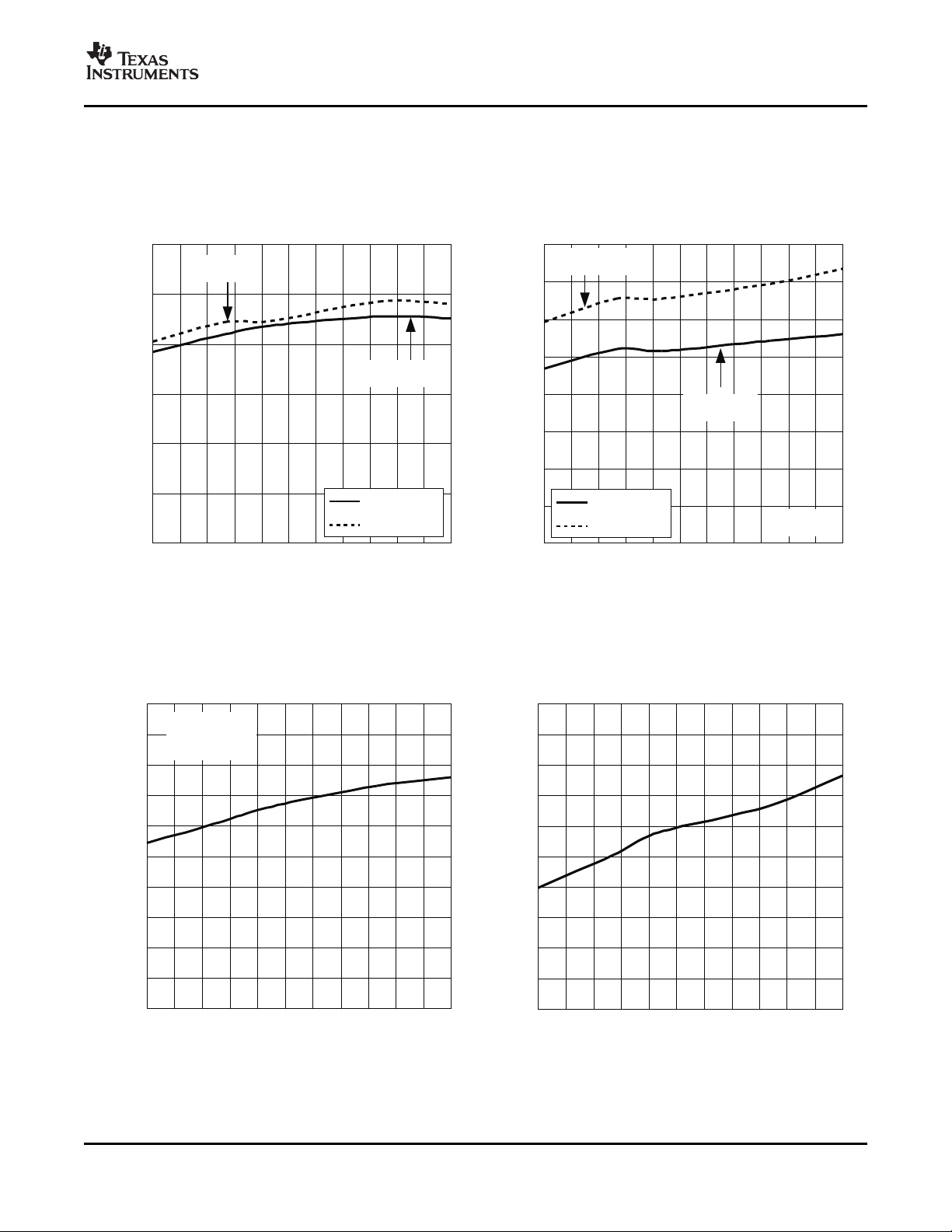
INPUT CURRENT OPERATING CURRENT IN SHUTDOWN
vs vs
JUNCTION TEMPERATURE JUNCTION TEMPERATURE
TPS40195
SLUS720 – FEBRUARY 2007
Figure 1. Figure 2.
POWERGOOD LEAKAGE CURRENT CURRENT LIMIT OFFSET VOLTAGE
vs vs
JUNCTION TEMPERATURE JUNCTION TEMPERATURE
Figure 3. Figure 4.
Submit Documentation Feedback
5
www.ti.com
0.4 0.6 0.8 1.0 1.2 1.4 1.6
0
0.5
3.0
3.5
4.5
1.5
1.0
5.0
2.0
2.5
4.0
1-D - Freewheel Time - ms
I
OC
- Relative Overcurrent Trip Point - A
0
0.5
1.0
1.5
2.0
2.5
-40 -25 -10 5 20 35 95 12550 65 80 110
3.0
On
Off
Off
On
TJ- Junction Temperature - °C
V
IN,
V
IL
- Enable Thresholds Voltage - V
93
94
92
91
90
99
100
98
97
95
-40 -25 -10 5 20 35 95 12550 65 80 110
96
I
BP
- Short Circuit Current - mA
TJ- Junction Temperature - °C
-40 -25 -10 5 20 35 95 125
-10
-8
0
2
6
-6
-4
-2
4
50 65 80 110
BP
GND
100 kW
BP
100 kW
GND
TJ- Junction Temperature - °C
f
SW
- Switching Frequency Change - %
TPS40195
SLUS720 – FEBRUARY 2007
TYPICAL CHARACTERISTICS (continued)
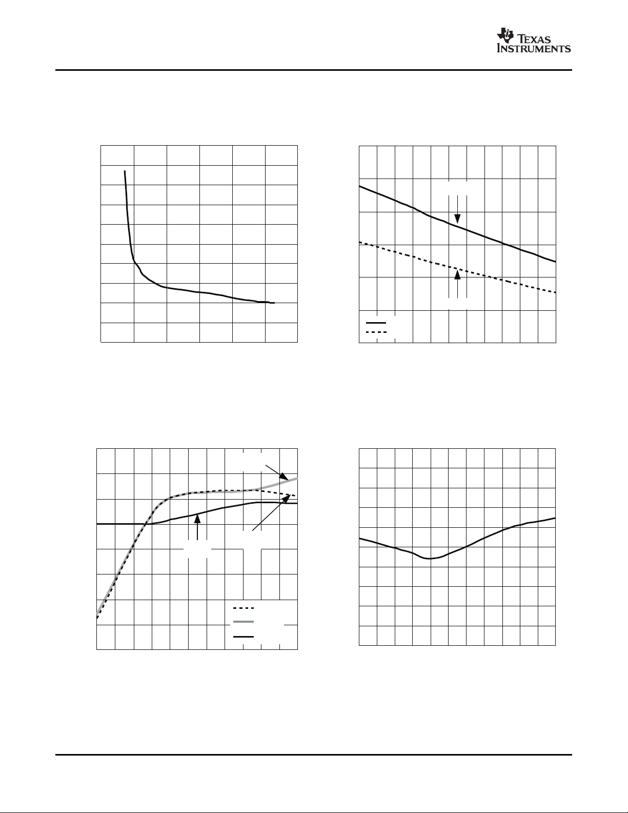
RELATIVE OVERCURRENT TRIP POINT EN THRESHOLD VOLTAGES
vs vs
FREEWHEEL TIME JUNCTION TEMPERATURE
Figure 5. Figure 6.
SWITCHING FREQUENCY CHANGE BP SHORT CIRCUIT CURRENT
vs vs
JUNCTION TEMPERATURE JUNCTION TEMPERATURE
6
Figure 7. Figure 8.
Submit Documentation Feedback
www.ti.com
1.25
-40 -25 -10 5 20 35 95 12550 65 80 110
1.26
1.27
1.29
1.28
1.30
TJ- Junction Temperature - °C
V
UVLO
- Undervoltage Lockout Threshold - V
0
-40 -25 -10 5 20 35 95 12550 65 80 110
200
350
450
500
250
100
150
300
400
50
V
DO
- Dropout Voltage - V
TJ- Junction Temperature - °C
V
VDD
= 5 V
I
LOAD
= 25 mA
4.0
4.2
4.8
5.4
5.8
6.0
5.2
4.6
-40 -25 -10 5 20 35 95 12550 65 80 110
4.4
5.6
5.0
V
UVLO
= 1.375 V
TJ- Junction Temperature - °C
I
UVLO
- Hysteresis Current - mA
3.5
3.6
3.8
3.7
-40 -25 -10 5 20 35 95 12550 65 80 110
3.9
4.1
4.2
3.3
3.2
3.4
4.0
TJ- Junction Temperature - °C
V
UVLOBP
- Bypass Undervoltage Lockout Voltage - V
Turn Off
Turn On
TYPICAL CHARACTERISTICS (continued)
TPS40195
SLUS720 – FEBRUARY 2007
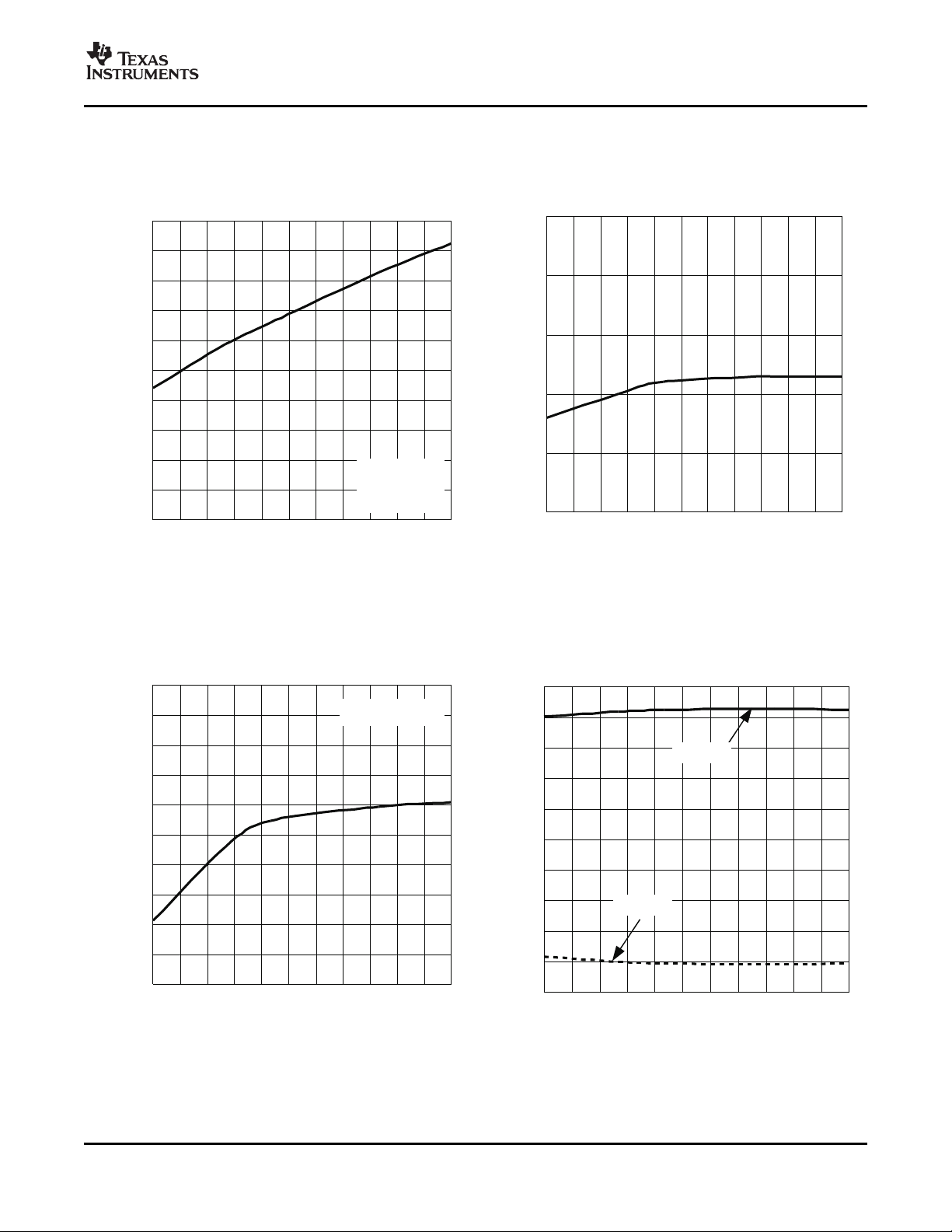
BP DROPOUT VOLTAGE UNDERVOLTAGE LOCKOUT THRESHOLD
vs vs
JUNCTION TEMPERATURE JUNCTION TEMPERATURE
Figure 9. Figure 10.
UNDERVOLTAGE LOCKOUT HYSTERESIS BP UNDERVOLTAGE LOCKOUT VOLTAGE
JUNCTION TEMPERATURE JUNCTION TEMPERATURE
Figure 11. Figure 12.
vs vs
Submit Documentation Feedback
7
www.ti.com
-40 -25 -10 5 20 35 95 12550 65 80 110
-0.6
-0.5
-0.4
0
0.1
0.3
-0.3
-0.2
-0.1
0.4
0.5
0.2
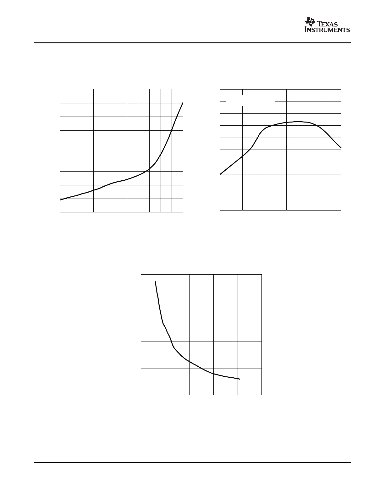
V
FB
- Feedback Voltage Reference Change - %
VFB= 591 mV (typ)
-20
-15
-5
-10
-40 -25 -10 5 20 35 95 12550 65 80 110
0
5
10
20
15
25
TJ- Junction Temperature - °C
I
FB
- Feedback Bias Current - nA
0 50 100 150 200 250
R
RT
- TIming Resistance - kW
f
OSC
- Oscillator Frequency - kHz
0
100
300
400
600
800
900
500
700
200
TPS40195
SLUS720 – FEBRUARY 2007
TYPICAL CHARACTERISTICS (continued)
FEEDBACK BIAS CURRENT RELATIVE FEEDBACK VOLTAGE CHANGE
vs vs
JUNCTION TEMPERATURE JUNCTION TEMPERATURE
Figure 13. Figure 14.
8
OSCILLATOR FREQUENCY
vs
TIMING RESISTANCE
Figure 15.
Submit Documentation Feedback

www.ti.com
1
2
3
4
5
6
7
8
16
15
14
13
12
11
10
9
EN
FB
COMP
VDD
UVLO
RT
ILIM
GND
HDRV
SW
BOOT
LDRV
BP
SS_SEL
PGOOD
SYNC
PW PACKAGE
(TOP VIEW)
TPS40195
SLUS720 – FEBRUARY 2007
DEVICE INFORMATION
TERMINAL FUNCTIONS
TERMINAL
NAME NO.
BOOT 14 I
BP 12 O Larger capacitors, up to 4.7 µ F will improve noise performance with a low side FET Qg over 25nC. Do not
COMP 3 O Output of the error amplifier.
EN 1 I controller on. A weak internal pull-up holds this pin high so that the pin may be left floating if this function is
FB 2 I
GND 8 - Common reference for the device
HDRV 16 O Gate drive output to the high-side N-channel FET.
ILIM 7 I
LDRV 13 O Gate drive output for the low side N-channel FET.
PGOOD 10 O
RT 6 I output. Connect a resistor to GND to program a frequency and allow SYNC to accept synchronization
SS_SEL 11 I
SW 15 I
SYNC 9 I/O
UVLO 5 I
VDD 4 I Power input to the controller. A 100 nF bypass capacitor should be connected closely from this pin to GND.
I/O DESCRIPTION
Gate drive voltage for the high-side N-channel MOSFET. A 100-nF capacitor (typical) must be connected
between this pin and SW.
Output bypass for the internal regulator. Connect a capacitor of 1- µ F (or greater) from this pin to GND.
connect to VDD or drive externally.
Logic level input which starts or stops the controller from an external user command. A high-level turns the
not used. Observe interface cautions in applications information.
Inverting input to the error amplifier. In normal operation the voltage on this pin is equal to the internal
reference voltage (591 mV typical)
Current limit. Sets short circuit protection threshold for low-side MOSFET sensing. Connect a resistor to
GND to set the threshold
Open drain power good output. Pulls low under any fault condition, soft start is active or if the FB pin
voltage is outside the specified voltage window.
Switching frequency programming pin. Also determines function of SYNC pin. Connected to GND for 250
kHz operation and using SYNC as an output. Connect to BP for 500-kHz operation and using SYNC as an
pulses. If RT is used to program a switching frequency and SYNC is not to be used to synchronize the
converter to an external clock, connect SYNC to GND.
Soft-start timing selection. Can be connected to GND, BP or left floating to select a soft start time that is
proportional to the switching frequency.
Sense line for the adaptive anti-cross conduction circuitry. Serves as common connection for the flying
high-side MOSFET driver
Bidirectional synchronization I/O pin. SYNC is an output when the RT pin is connected to BP or GND. The
output is a falling edge signal 180 ° out-of-phase with the rising edge of HDRV. In this mode SYNC can be
used to drive the SYNC pin of an additional TPS40195 device whose RT pin is tied to GND through a
resistor, providing two converters that operate 180 ° out-of-phase to one another. SYNC may be used as an
input to synchronize to an external system clock if RT is connected to GND through a resistor as well. The
device synchronizes to the falling edge of the external clock signal. If RT is used to program a switching
frequency and SYNC is not to be used to synchronize the converter to an external clock, connect SYNC to
GND.
Programmable UVLO pin for the controller. A resistor divider on this pin to VDD sets the converter turn on
voltage and the hysteresis for turn-off.
Submit Documentation Feedback
9
www.ti.com
UDG-06065
EN 1
VDD 4
BP
12
COMP
3
FB
2
GND 8
5 V
Regulator
1.26 V
+
BP, 5 V
+
Error
Amplifier
591 mV
SS
Fault
Controller
Soft Start
Ramp
Generator
PWM Logic
and
Anti-Cross
Conduction
+
Oscillator
SD
UVLO
SS
FAULT
UVLO
+
CLK
16
CLK
14
13
15
10
BOOT
HDRV
SW
LDRV
PGOOD
BP
Powergood
Control
SS ACTIVE
SD
FAULT
BP
750 kW
VDD
SS
SD
+
Overtemperature
11
9 mA
BP
7 ILIM
+
VDD
SC_LOW
SC_HIGH
5UVLO
5.2 mA
+
+
0.53 V
RT
5
SYNC
6
0.65 V
SD
SS_SEL
BUF
550 mV
1.5 MW
TPS40195
SLUS720 – FEBRUARY 2007
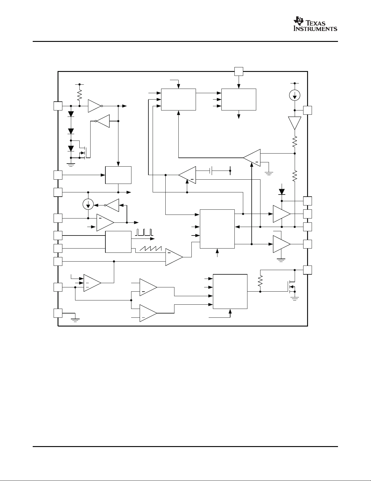
BLOCK DIAGRAM
10
Submit Documentation Feedback
www.ti.com
4
1
8
1.5 MW
200 W
200 kW
1 kW
1 kW
300 kW
To
Enable
Chip
VDD
EN
GND
UDG-07005
TPS40195
SLUS720 – FEBRUARY 2007
APPLICATION INFORMATION
Introduction
The TPS40195 is a flexible controller providing all the necessary features to construct a high performance
DC-DC converter while keeping costs to a minimum. Support for pre-biased outputs eliminates concerns about
damaging sensitive loads during startup. Strong gate drivers for the high side and rectifier N channel FETs
decrease switching losses for increased efficiency. Adaptive gate drive timing minimizes body diode conduction
in the rectifier FET, also increasing efficiency. Selectable short circuit protection thresholds and hiccup recovery
from a short circuit increase design flexibility and minimize power dissipation in the event of a prolonged output
fault. A dedicated enable pin (EN) allows the converter to be placed in a low quiescent current shutdown mode.
Enable Functionality
The TPS40195 has a dedicated device enable (EN) pin. This simplifies user level interface design since no
multiplexed functions exist. Another benefit is a true low power shutdown mode of operation. When the EN pin is
pulled to GND, the TPS40195 consumes a typical 165- µ A of current. A functionally equivalent circuit to the
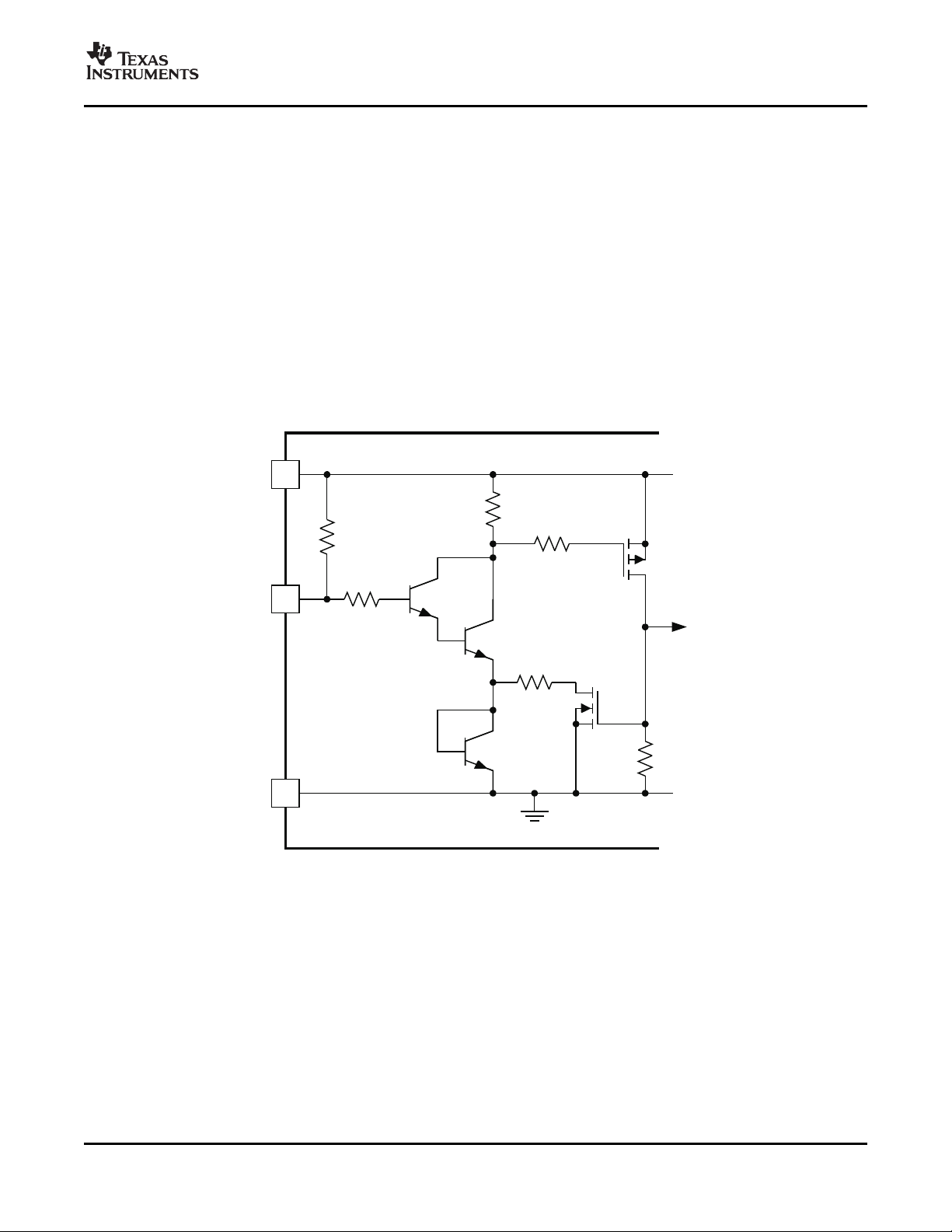
enable circuitry on the TPS40195 is shown in Figure 16 .
Figure 16. TPS40195 EN Pin Internal Circuitry
If the EN pin is left floating, the chip starts automatically. The pin must be pulled to less than 600 mV for the
TPS40195 to be in shutdown mode. Note that the EN pin is relatively high impedance. In some situations, there
could be enough noise nearby to cause the EN pin to swing below the 600 mV threshold and give erroneous
shutdown commands to the rest of the device. There are two solutions to this problem should it arise.
1. Place a capacitor from EN to GND. A side effect of this is to delay the start of the converter while the
capacitor charges past the enable threshold
2. Place a resistor from VDD to EN. This causes more current to flow in the shutdown mode, but does not
delay converter startup. If a resistor is used, the total current into the EN pin should be limited to no more
than 500 µ A.
Submit Documentation Feedback
11
www.ti.com
T-Time-500 ms/div
HDRV
(2V/div)
PGOOD
(2V/div)
VOUT
(1V/div)
EN
(1V/div)
( )
f
4
SW
RT
2.5 10
R
´
=
TPS40195
SLUS720 – FEBRUARY 2007
APPLICATION INFORMATION (continued)
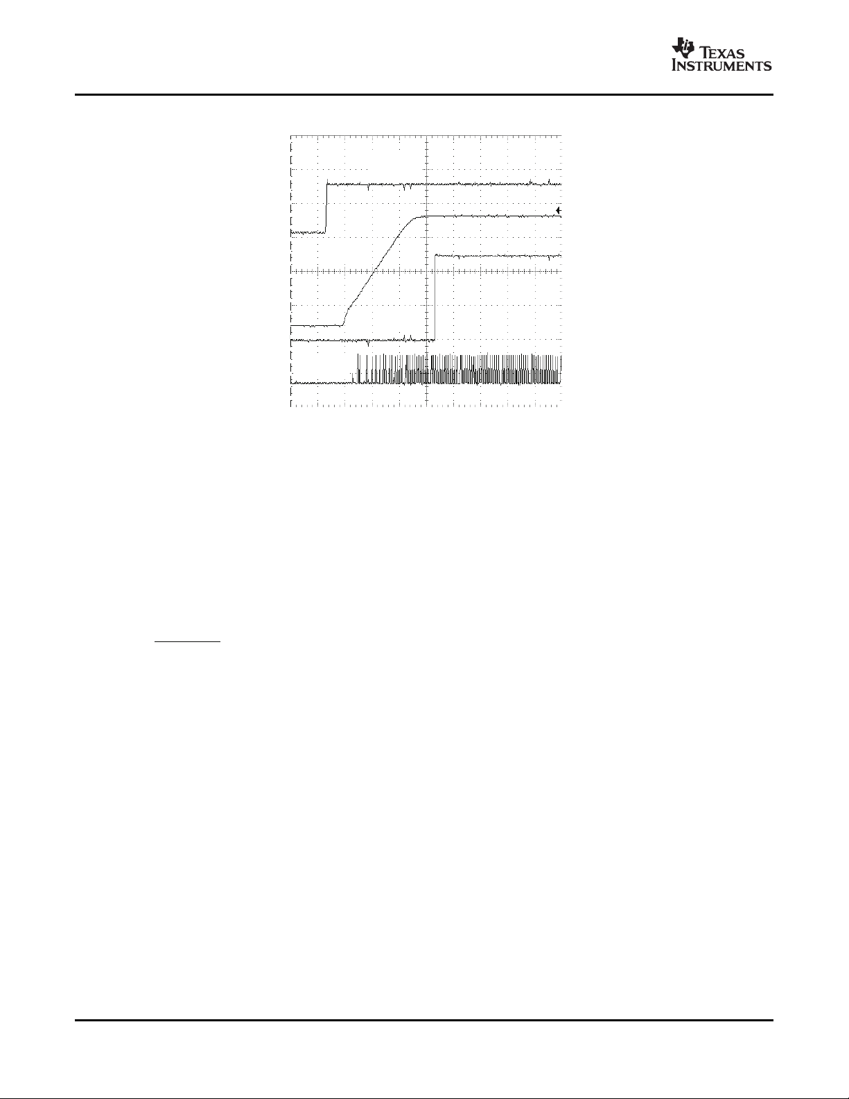
Figure 17. TPS40195 EN Pin Startup
Voltage Reference
The band gap cell is designed with a trimmed 0.591-V output. The 0.5% tolerance on the reference voltage
allows the user to design a very accurate power supply.
Oscillator and Synchronization
The TPS40195 has a programmable switching frequency of 100 kHz to 600 kHz using a resistor connected from
the RT pin to GND. The relationship between switching frequency and the resistor from RT to GND is given in
Equation 1 .
where
• fSWis the switching frequency in kHz
• R
When the oscillator is programmed using this method, the SYNC pin is configured as an input. The device may
be synchronized to a higher frequency than the free running frequency by applying a pulse train to the SYNC
pin. For best results, limit the frequency of the pulse train applied to SYNC to 20% more than the free running
frequency. The TPS40195 will synchronize to the falling edge of the pulse train applied to the SYNC pin.
is the resistor connected from RT to GND in k Ω
RT
(1)
12
Submit Documentation Feedback
 Loading...