

Page 1
www.ti.com
1
2
3
4
EN
FB
COMP
VDD
TPS40195
5
6
7
8
ULVO
RT
ILIM
GND
16
15
14
13
HDRV
SW
BOOT
LDRV
12
11
10
9
BP
SS_SEL
PGOOD
SYNC
Power Good
V
OUT
UDG-06066
SLUS720A – FEBRUARY 2007 – REVISED JULY 2007
4.5-V TO 20-V SYNCHRONOUS BUCK CONTROLLER WITH SYNCHRONIZATION AND
POWER GOOD
FEATURES CONTENTS
• Input Operating Voltage Range: 4.5 V to 20 V
• Output Voltage as Low as 0.591 V ± 0.5%
• 180 ° Bi-Directional Out-of-Phase
Synchronization
• Internal 5-V Regulator
• High and Low MOSFET Sense Overcurrent Design Example 21
• 100 kHz to 600 kHz Switching Frequency
• Enable and Power Good
• Programmable UVLO and Hysteresis
• Thermal Shutdown at 150 ° C
• Selectable Soft-Start
• Pre-Bias Output Safe
APPLICATIONS
• Digital TV
• Entry-Level and Midrange Servers
• Networking Equipment
• Non-Isolated DC-DC modules
Device Ratings 2
Electrical Characteristics 3
Typical Characteristics 5
Terminal Information 10
Application Information 12
Additional References 34
DESCRIPTION
The TPS40195 is a flexible synchronous buck
controller that operates from a nominal 4.5 V to 20 V
supply. This controller implements voltage mode
control with the switching frequency adjustable from
100 kHz to 600 kHz. Flexible features found on this
device include selectable soft-start time,
programmable short circuit limit, programmable
undervoltage lockout (UVLO) and synchronization
capability. An adaptive anti-cross conduction scheme
is used to prevent shoot through current in the power
FETs. Short-circuit detection is done by sensing the
voltage drop across the low-side MOSFET when it is
on, and comparing it with a user programmable
threshold.
TPS40195
Please be aware that an important notice concerning availability, standard warranty, and use in critical applications of Texas
Instruments semiconductor products and disclaimers thereto appears at the end of this data sheet.
PRODUCTION DATA information is current as of publication date.
Products conform to specifications per the terms of the Texas
Instruments standard warranty. Production processing does not
necessarily include testing of all parameters.
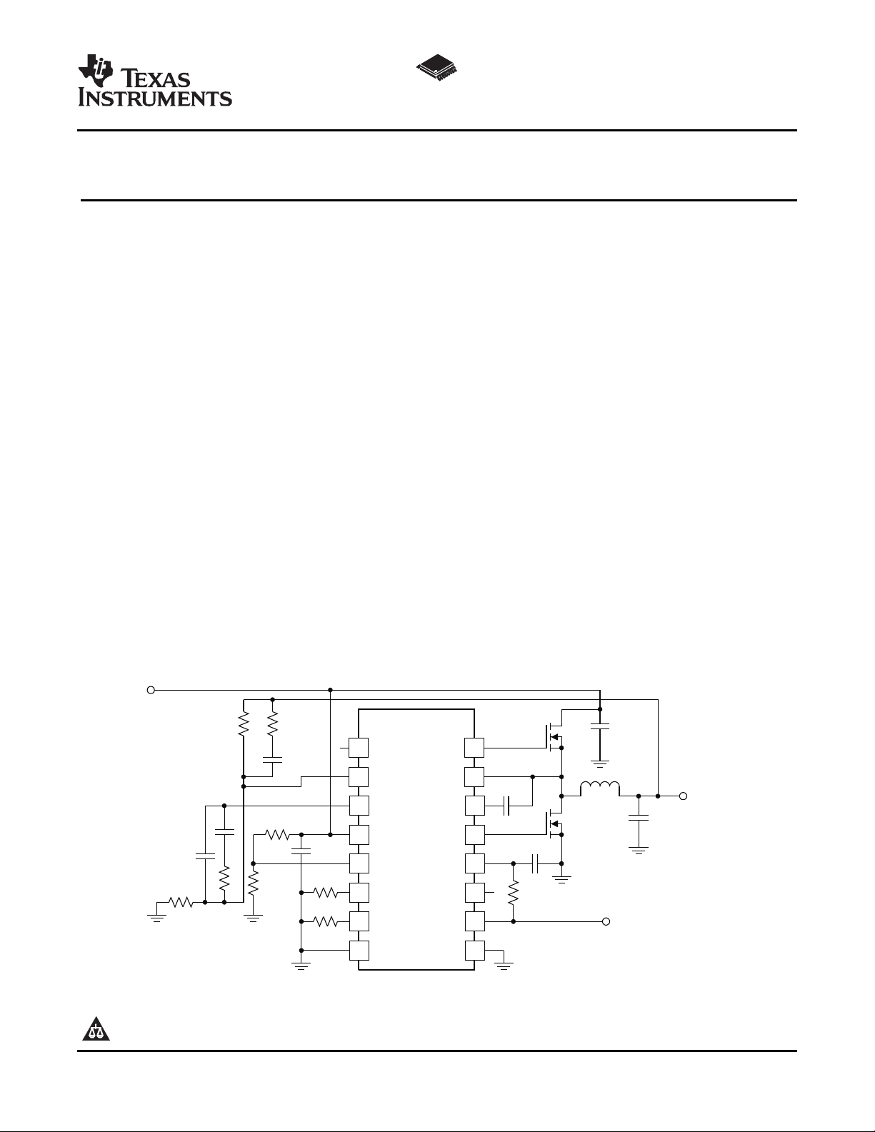
SIMPLIFIED APPLICATION DIAGRAM
Copyright © 2007, Texas Instruments Incorporated
Page 2

www.ti.com
TPS40195
SLUS720A – FEBRUARY 2007 – REVISED JULY 2007
These devices have limited built-in ESD protection. The leads should be shorted together or the device placed in conductive foam
during storage or handling to prevent electrostatic damage to the MOS gates.
DESCRIPTION (CONTINUED)
The threshold is set with a single external resistor connected from ILIM to GND. Pulse-by-pulse limiting (to
prevent current runaway) is provided by sensing the voltage across the high-side MOSFET when it is on and
terminating the cycle when the voltage drop rises above a fixed threshold of 550 mV. When the controller
senses an output short circuit, both MOSFETs are turned off and a timeout period is observed before attempting
to restart. This provides limited power dissipation in the event of a sustained fault. Synchronization on this
device is bi-directional. Devices can be synchronized 180 ° out of phase to a chosen master TPS40195 running
at a fixed 250 kHz or 500 kHz, or can be synchronized to an outside clock source anywhere in the 100 kHz to
600 kHz range.
ORDERING INFORMATION
T
J
-40 ° C to 85 ° C
(1) For the most current package and ordering information, see the Package Option Addendum at the end of this document, or see the TI
website at www.ti.com .
PACKAGE QUANTITY PACKAGING
Plastic 16-Pin TSSOP
(PW)
Plastic 16-Pin QFN
(RGY)
90 Tube TPS40195PW
2000 Reel TPS40195PWR
250 Tape TPS40195RGYT
3000 Reel TPS40195RGYR
(1)
PART NUMBER
DEVICE RATINGS
ABSOLUTE MAXIMUM RATINGS
over operating free-air temperature range unless otherwise noted
VDD –0.3 to 22
SW –5 to 25
BOOT –0.3 to 30
Input voltage range HDRV –5 to 30 V
BOOT–SW, HDRV–SW (Differential from BOOT or HDRV to SW) –0.3 to 6
EN, FB, BP, LDRV, PGOOD, ILIM, SYNC, UVLO, SS_SEL, RT –0.3 to 6
COMP –0.3 to 3
T
Operating junction temperature range –40 to 150
J
T
Storage temperature –55 to 150
stg
(1) Stresses beyond those listed under "absolute maximum ratings" may cause permanent damage to the device. These are stress ratings
only, and functional operation of the device at these or any other conditions beyond those indicated under "recommended operating
conditions" is not implied. Exposure to absolute-maximum-rated conditions for extended periods may affect device reliability.
(1)
TPS40195 UNIT
RECOMMENDED OPERATING CONDITIONS
MIN NOM MAX UNIT
V
Input voltage 4.5 20 V
VDD
T
Operating junction temperature -40 125 ° C
J
° C
2
Submit Documentation Feedback
Page 3
www.ti.com
TPS40195
SLUS720A – FEBRUARY 2007 – REVISED JULY 2007
PACKAGE DISSIPATION RATINGS
R
High-K Board
PACKAGE AIRFLOW (LFM)
θ JA
( ° C/W) TA= 25 ° C TA= 85 ° C
PW 0 (Natural Convection) 110 0.90 0.36
0 (Natural Convection) 49.2 2.0 0.81
RGY 200 41.2 2.4 0.97
400 37.7 2.6 1.0
(1) Ratings based on JEDEC High Thermal Conductivity (High K) Board. For more information on the test method, see TI Technical Brief
SZZA017 .
ELECTROSTATIC DISCHARGE (ESD) PROTECTION
Human Body Model (HBM) 2500
Charged Device Model (CDM) 1500
ELECTRICAL CHARACTERISTICS
TJ= –40 ° C to 85 ° C, V
REFERENCE
V
FB
INPUT SUPPLY
V
VDD
I
VDD
ON BOARD REGULATOR
V
BP
V
DO
I
SC
I
BP
OSCILLATOR
f
SW
V
RMP
SYNCHRONIZATION
V
INH
V
INL
T
F(max)
V
OH
V
OL
T
F
T
R
(1) Specified by design. Not production tested.
Feedback voltage range mV
Input voltage range 4.5 20.0 V
Operating current V
Output voltage V
Regulator dropout voltage, V
Regulator current limit threshold 75
Average current 75
Switching frequency V
Ramp amplitude
High-level input voltage 2.5
Low-level input voltage 0.5
Maximum input fall time
High-level output voltage I
Low-level output voltage I
Output rise time
Output fall time
= 12 Vdc, all parameters at zero power dissipation (unless otherwise noted)
VDD
PARAMETER TEST CONDITIONS MIN TYP MAX UNIT
0 ° C ≤ TJ≤ 85 ° C 588 591 594
-40 ° C ≤ TJ≤ 85 ° C 585 591 594
V
= 3 V 4 mA
EN
< 0.6 V, V
EN
V
< 0.6 V, V
EN
> 6 V, IBP≤ 10 mA 5.1 5.3 5.5 V
VDD
- V
VDD
(1)
(1)
(1)
(1)
V
BP
= 5 V, IBP≤ 25 mA 350 550 mV
VDD
V
= V
RT
= 0 V 200 250 290 kHz
RT
R
= 100 k Ω 250
RT
= 100 μ A, sourcing 3.5
SYNC
= 100 μ A, sinking 0.3
SYNC
C
SYNC
VDD
VDD
BP
=25 pF ns
(1)
Power Rating (W) Power Rating (W)
MIN TYP MAX UNIT
= 12 V 165 250
= 20 V 230 330
400 500 580
1 V
10 25
100 300
100 ns
V
μ A
mA
V
V
Submit Documentation Feedback
3
Page 4
www.ti.com
TPS40195
SLUS720A – FEBRUARY 2007 – REVISED JULY 2007
ELECTRICAL CHARACTERISTICS (continued)
TJ= –40 ° C to 85 ° C, V
PWM
D
MAX
t
ON(min)
t
DEAD
SOFT-START
t
SS
ERROR AMPLIFIER
GBWP Gain bandwidth product
A
OL
I
IB
I
EAOP
I
EAOM
SHORT CIRCUIT PROTECTION
t
PSS(min)
t
BLNK
t
OFF
I
ILIM
V
ILIMOFST
V
ILIMH
OUTPUT DRIVERS
R
HDHI
R
HDLO
R
LDHI
R
LDLO
t
HRISE
t
HFALL
t
LRISE
t
LFALL
UVLO
V
UVLOBP
V
UVLOBPH
V
UVLO
I
UVLO
SHUTDOWN
V
IH
V
IL
Maximum duty cycle
Minimum controlled pulse
Output driver dead time
Soft-start time ms
DC gain
Input bias current (current out of FB
pin)
Output source current V
Output sink current V
Minimum pulse during short circuit
Blanking time
Off-time between restart attempts 40 ms
ILIM pin bias current TJ= 25 ° C 7 9 11 μ A
Low side comparator offset voltage -20 0 20 mV
Short circuit threshold voltage on
high-side MOSFET
High-side driver pull-up resistance V
High-side driver pull-down resistance V
Low-side driver pull-up resistance I
Low-side driver pull-down resistance I
High-side driver rise time
High-side driver fall time
Low-side driver rise time
Low-side driver fall time
BP5 UVLO threshold voltage 3.9 4.1 4.3 V
BP5 UVLO hysteresis voltage 800 mV
Turn-on voltage 1.125 1.26 1.375 V
UVLO pin hysteresis current V
High-level input voltage, EN 1.9 3
Low-level input voltage, EN 0.6
= 12 Vdc, all parameters at zero power dissipation (unless otherwise noted)
VDD
PARAMETER TEST CONDITIONS MIN TYP MAX UNIT
(1)
(1)
(1)
85%
(1)
130
HDRV off to LDRV on 50 ns
LDRV off to HDRV on 25
V
V
V
V
V
V
(1)
= 0 V, fSW= 250 kHz 4.8
SS_SEL
= 0 V, fSW= 500 kHz 2.4
SS_SEL
= Floating, fSW= 250 kHz 2.4
SS_SEL
= Floating, fSW= 500 kHz 1.2
SS_SEL
= VBP, fSW= 250 kHz 1.2
SS_SEL
= VBP, fSW= 500 kHz 0.6
SS_SEL
7 10 MHz
60 dB
100 nA
= 0 V 1
FB
= 2 V 1
FB
(1)
250
60 90 120
mA
ns
TJ= 25 ° C 400 550 650 mV
- V
BOOT
BOOT
LDRV
(1)
(1)
(1)
(1)
LDRV
C
LOAD
UVLO
= 4.5 V, I
SW
- V
= 4.5 V, I
SW
= -100 mA 2.5 5.0
= 100 mA 0.8 1.5
= 1 nF ns
= 1.375 V 5.2 μ A
= -100 mA 3 6
HDRV
= 100 mA 1.5 3.0
HDRV
Ω
15 35
10 25
15 35
10 25
V
(1) Specified by design. Not production tested.
4
Submit Documentation Feedback
Page 5
www.ti.com
ELECTRICAL CHARACTERISTICS (continued)
TJ= –40 ° C to 85 ° C, V
POWER GOOD
V
OV
V
UV
V
PG_HYST
R
PGD
I
PDGLK
BOOT DIODE
V
DFWD
THERMAL SHUTDOWN
T
JSD
T
JSDH
(1) Specified by design. Not production tested.
Feedback voltage limit for power good 650
Feedback voltage limit for power good 530
Powergood hysteresis voltage at FB
pin
Pulldown resistance of PGD pin V
Leakage current 530 mV ≤ V
Bootstrap diode forward voltage I
Junction shutdown temperature
Hysteresis
= 12 Vdc, all parameters at zero power dissipation (unless otherwise noted)
VDD
PARAMETER TEST CONDITIONS MIN TYP MAX UNIT
(1)
TPS40195
SLUS720A – FEBRUARY 2007 – REVISED JULY 2007
mV
30
< 530 mV or V
FB
FB
= 5 mA 0.5 0.8 1.2 V
BOOT
(1)
> 650 mV 7 20 Ω
FB
≤ 650 mV V
= 5V 7 12 μ A
PGOOD
150
20
° C
Submit Documentation Feedback
5
Page 6
www.ti.com
0
1.0
2.0
2.5
3.0
1.5
-40 -25 -10 5 20 35 95 12550 65 80 110
0.5
I
DD
- Input Current - mA
V
VDD
= 12V
V
VDD
= 20V
V
VDD
= 12 V
V
VDD
= 20 V
T
J
- Junction Temperature - °C
150
200
300
350
400
250
100
50
0
-40 -25 -10 5 20 35 95 12550 65 80 110
V
VDD
= 12 V
V
VDD
= 20 V
VEN= 0 V
V
VDD
= 12V
V
VDD
= 20V
T
J
- Junction Temperature - °C
I
DD
- Operating Current in Shutdown - mA
-10
-9
-6
-5
-3
-1
0
-4
-8
-40 -25 -10 5 20 35 95 12550 65 80 110
-7
-2
T
J
- Junction Temperature - °C
V
ILIMOFST
- Current Limit Offset Voltage - mV
-40 -25 -10 5 20 35 9550 65 80 110 125
0
1
2
3
10
4
5
6
7
9
8
T
J
- Junction Temperature - °C
I
PGDLK
- Powergood Leakage Current - mA
V
PGOOD
= 5 V
V
FB
= 590 mV
TPS40195
SLUS720A – FEBRUARY 2007 – REVISED JULY 2007
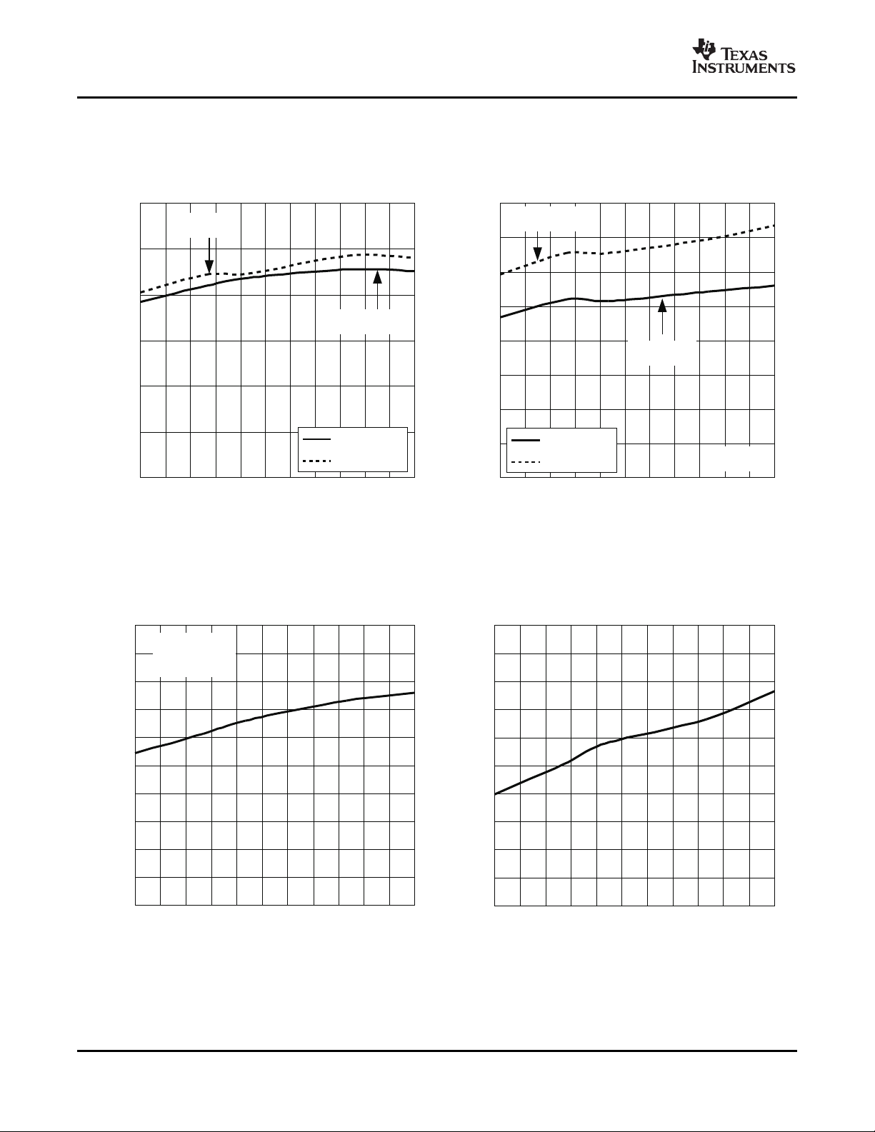
INPUT CURRENT OPERATING CURRENT IN SHUTDOWN
JUNCTION TEMPERATURE JUNCTION TEMPERATURE
TYPICAL CHARACTERISTICS
vs vs
Figure 1. Figure 2.
POWERGOOD LEAKAGE CURRENT CURRENT LIMIT OFFSET VOLTAGE
vs vs
JUNCTION TEMPERATURE JUNCTION TEMPERATURE
6
Figure 3. Figure 4.
Submit Documentation Feedback
Page 7
www.ti.com
0.4 0.6 0.8 1.0 1.2 1.4 1.6
0
0.5
3.0
3.5
4.5
1.5
1.0
5.0
2.0
2.5
4.0
1-D - Freewheel Time - ms
I
OC
- Relative Overcurrent Trip Point - A
0
0.5
1.0
1.5
2.0
2.5
-40 -25 -10 5 20 35 95 12550 65 80 110
3.0
On
Off
Off
On
TJ- Junction Temperature - °C
V
IN,
V
IL
- Enable Thresholds Voltage - V
93
94
92
91
90
99
100
98
97
95
-40 -25 -10 5 20 35 95 12550 65 80 110
96
I
BP
- Short Circuit Current - mA
TJ- Junction Temperature - °C
-40 -25 -10 5 20 35 95 125
-10
-8
0
2
6
-6
-4
-2
4
50 65 80 110
BP
GND
100 kW
BP
100 kW
GND
TJ- Junction Temperature - °C
f
SW
- Switching Frequency Change - %
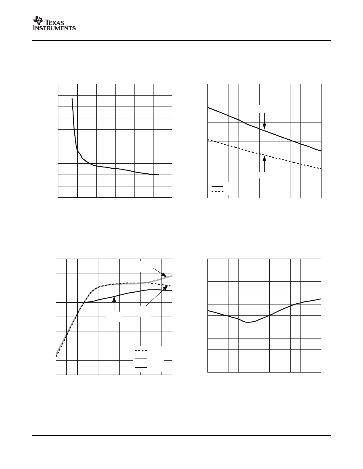
TYPICAL CHARACTERISTICS (continued)
TPS40195
SLUS720A – FEBRUARY 2007 – REVISED JULY 2007
RELATIVE OVERCURRENT TRIP POINT EN THRESHOLD VOLTAGES
vs vs
FREEWHEEL TIME JUNCTION TEMPERATURE
Figure 5. Figure 6.
SWITCHING FREQUENCY CHANGE BP SHORT CIRCUIT CURRENT
vs vs
JUNCTION TEMPERATURE JUNCTION TEMPERATURE
Figure 7. Figure 8.
Submit Documentation Feedback
7
Page 8
www.ti.com
1.25
-40 -25 -10 5 20 35 95 12550 65 80 110
1.26
1.27
1.29
1.28
1.30
TJ- Junction Temperature - °C
V
UVLO
- Undervoltage Lockout Threshold - V
0
-40 -25 -10 5 20 35 95 12550 65 80 110
200
350
450
500
250
100
150
300
400
50
V
DO
- Dropout Voltage - V
TJ- Junction Temperature - °C
V
VDD
= 5 V
I
LOAD
= 25 mA
4.0
4.2
4.8
5.4
5.8
6.0
5.2
4.6
-40 -25 -10 5 20 35 95 12550 65 80 110
4.4
5.6
5.0
V
UVLO
= 1.375 V
TJ- Junction Temperature - °C
I
UVLO
- Hysteresis Current - mA
3.5
3.6
3.8
3.7
-40 -25 -10 5 20 35 95 12550 65 80 110
3.9
4.1
4.2
3.3
3.2
3.4
4.0
TJ- Junction Temperature - °C
V
UVLOBP
- Bypass Undervoltage Lockout Voltage - V
Turn Off
Turn On
TPS40195
SLUS720A – FEBRUARY 2007 – REVISED JULY 2007
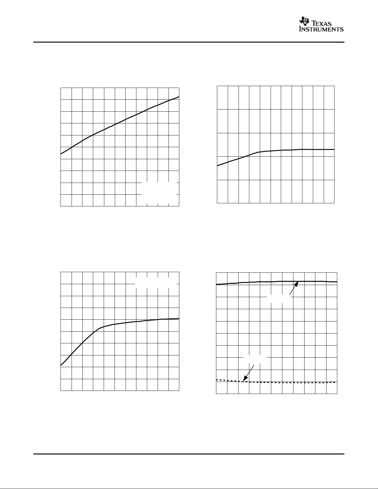
TYPICAL CHARACTERISTICS (continued)
BP DROPOUT VOLTAGE UNDERVOLTAGE LOCKOUT THRESHOLD
vs vs
JUNCTION TEMPERATURE JUNCTION TEMPERATURE
Figure 9. Figure 10.
UNDERVOLTAGE LOCKOUT HYSTERESIS BP UNDERVOLTAGE LOCKOUT VOLTAGE
JUNCTION TEMPERATURE JUNCTION TEMPERATURE
8
Figure 11. Figure 12.
vs vs
Submit Documentation Feedback
Page 9
www.ti.com
-40 -25 -10 5 20 35 95 12550 65 80 110
-0.6
-0.5
-0.4
0
0.1
0.3
-0.3
-0.2
-0.1
0.4
0.5
0.2
V
FB
- Feedback Voltage Reference Change - %
VFB= 591 mV (typ)
-20
-15
-5
-10
-40 -25 -10 5 20 35 95 12550 65 80 110
0
5
10
20
15
25
TJ- Junction Temperature - °C
I
FB
- Feedback Bias Current - nA
0 50 100 150 200 250
R
RT
- TIming Resistance - kW
f
OSC
- Oscillator Frequency - kHz
0
100
300
400
600
800
900
500
700
200
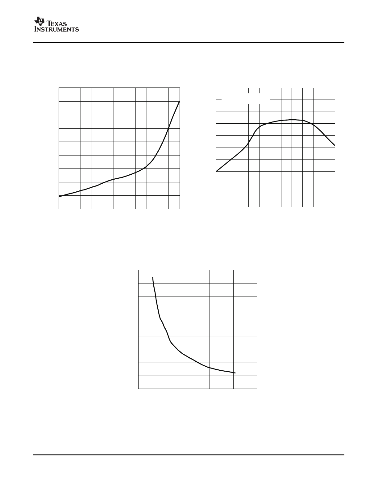
TYPICAL CHARACTERISTICS (continued)
TPS40195
SLUS720A – FEBRUARY 2007 – REVISED JULY 2007
FEEDBACK BIAS CURRENT RELATIVE FEEDBACK VOLTAGE CHANGE
vs vs
JUNCTION TEMPERATURE JUNCTION TEMPERATURE
Figure 13. Figure 14.
OSCILLATOR FREQUENCY
TIMING RESISTANCE
Submit Documentation Feedback
vs
Figure 15.
9
Page 10
www.ti.com
FB
1
2
3
4
5
6
7
8
16
15
14
13
12
11
10
9
EN
VDD
COMP
RT
UVLO
GND
ILIM
SW
HDRV
LDRV
BOOT
SS_SEL
BP
SYNC
PGOOD
RGY Package
(Bottom View)
1
2
3
4
5
6
7
89
15
14
13
12
11
10
16
EN
FB
VDD
COMP
RT
UVLO
GND
ILIM
SW
HDRV
LDRV
BOOT
SS_SEL
BP
SYNC
PGOOD
PW Package
(Top View)
TPS40195
SLUS720A – FEBRUARY 2007 – REVISED JULY 2007
DEVICE INFORMATION
TERMINAL FUNCTIONS
TERMINAL
NAME NO.
BOOT 14 I
BP 12 O Larger capacitors, up to 4.7 μ F will improve noise performance with a low side FET Qg over 25nC. Do not
COMP 3 O Output of the error amplifier.
EN 1 I controller on. A weak internal pull-up holds this pin high so that the pin may be left floating if this function is
FB 2 I
GND 8 - Common reference for the device
HDRV 16 O Gate drive output to the high-side N-channel FET.
ILIM 7 I
LDRV 13 O Gate drive output for the low side N-channel FET.
PGOOD 10 O
RT 6 I output. Connect a resistor to GND to program a frequency and allow SYNC to accept synchronization
SS_SEL 11 I
SW 15 I
SYNC 9 I/O
UVLO 5 I
VDD 4 I Power input to the controller. A 100 nF bypass capacitor should be connected closely from this pin to GND.
I/O DESCRIPTION
Gate drive voltage for the high-side N-channel MOSFET. A 100-nF capacitor (typical) must be connected
between this pin and SW.
Output bypass for the internal regulator. Connect a capacitor of 1- μ F (or greater) from this pin to GND.
connect to VDD or drive externally. This regulator is turned off when ENABLE is pulled low
Logic level input which starts or stops the controller from an external user command. A high-level turns the
not used. Observe interface cautions in applications information.
Inverting input to the error amplifier. In normal operation the voltage on this pin is equal to the internal
reference voltage (591 mV typical)
Current limit. Sets short circuit protection threshold for low-side MOSFET sensing. Connect a resistor to
GND to set the threshold
Open drain power good output. Pulls low under any fault condition, soft start is active or if the FB pin
voltage is outside the specified voltage window.
Switching frequency programming pin. Also determines function of SYNC pin. Connected to GND for 250
kHz operation and using SYNC as an output. Connect to BP for 500-kHz operation and using SYNC as an
pulses. If RT is used to program a switching frequency and SYNC is not to be used to synchronize the
converter to an external clock, connect SYNC to GND.
Soft-start timing selection. Can be connected to GND, BP or left floating to select a soft start time that is
proportional to the switching frequency.
Sense line for the adaptive anti-cross conduction circuitry. Serves as common connection for the flying
high-side MOSFET driver
Bidirectional synchronization I/O pin. SYNC is an output when the RT pin is connected to BP or GND. The
output is a falling edge signal 180 ° out-of-phase with the rising edge of HDRV. In this mode SYNC can be
used to drive the SYNC pin of an additional TPS40195 device whose RT pin is tied to GND through a
resistor, providing two converters that operate 180 ° out-of-phase to one another. SYNC may be used as an
input to synchronize to an external system clock if RT is connected to GND through a resistor as well. The
device synchronizes to the falling edge of the external clock signal. If RT is used to program a switching
frequency and SYNC is not to be used to synchronize the converter to an external clock, connect SYNC to
GND.
Programmable UVLO pin for the controller. A resistor divider on this pin to VDD sets the converter turn on
voltage and the hysteresis for turn-off.
10
Submit Documentation Feedback
Page 11
www.ti.com
UDG-06065
EN 1
VDD 4
BP
12
COMP
3
FB
2
GND 8
5 V
Regulator
1.26 V
+
BP, 5 V
+
Error
Amplifier
591 mV
SS
Fault
Controller
Soft Start
Ramp
Generator
PWM Logic
and
Anti-Cross
Conduction
+
Oscillator
SD
UVLO
SS
FAULT
UVLO
+
CLK
16
CLK
14
13
15
10
BOOT
HDRV
SW
LDRV
PGOOD
BP
Powergood
Control
SS ACTIVE
SD
FAULT
BP
750 kW
VDD
SS
SD
+
Overtemperature
11
9 mA
BP
7 ILIM
+
VDD
SC_LOW
SC_HIGH
5UVLO
5.2 mA
+
+
0.53 V
RT
5
SYNC
6
0.65 V
SD
SS_SEL
BUF
550 mV
1.5 MW
TPS40195
SLUS720A – FEBRUARY 2007 – REVISED JULY 2007
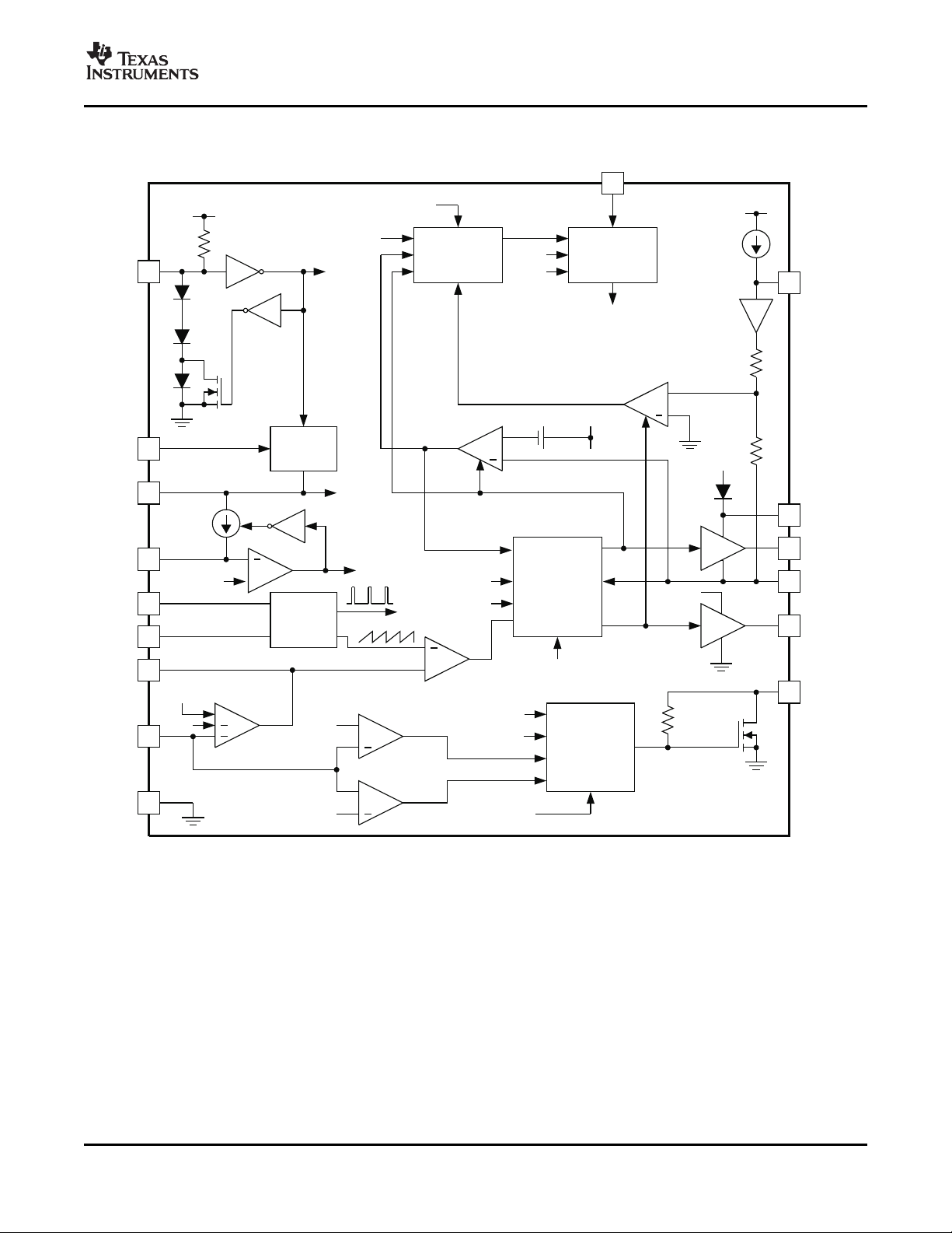
BLOCK DIAGRAM
Submit Documentation Feedback
11
Page 12
www.ti.com
4
1
8
1.5 MW
200 W
200 kW
1 kW
1 kW
300 kW
To
Enable
Chip
VDD
EN
GND
UDG-07005
TPS40195
SLUS720A – FEBRUARY 2007 – REVISED JULY 2007
APPLICATION INFORMATION
Introduction
The TPS40195 is a flexible controller providing all the necessary features to construct a high performance
DC-DC converter while keeping costs to a minimum. Support for pre-biased outputs eliminates concerns about
damaging sensitive loads during startup. Strong gate drivers for the high side and rectifier N channel FETs
decrease switching losses for increased efficiency. Adaptive gate drive timing minimizes body diode conduction
in the rectifier FET, also increasing efficiency. Selectable short circuit protection thresholds and hiccup recovery
from a short circuit increase design flexibility and minimize power dissipation in the event of a prolonged output
fault. A dedicated enable pin (EN) allows the converter to be placed in a low quiescent current shutdown mode.
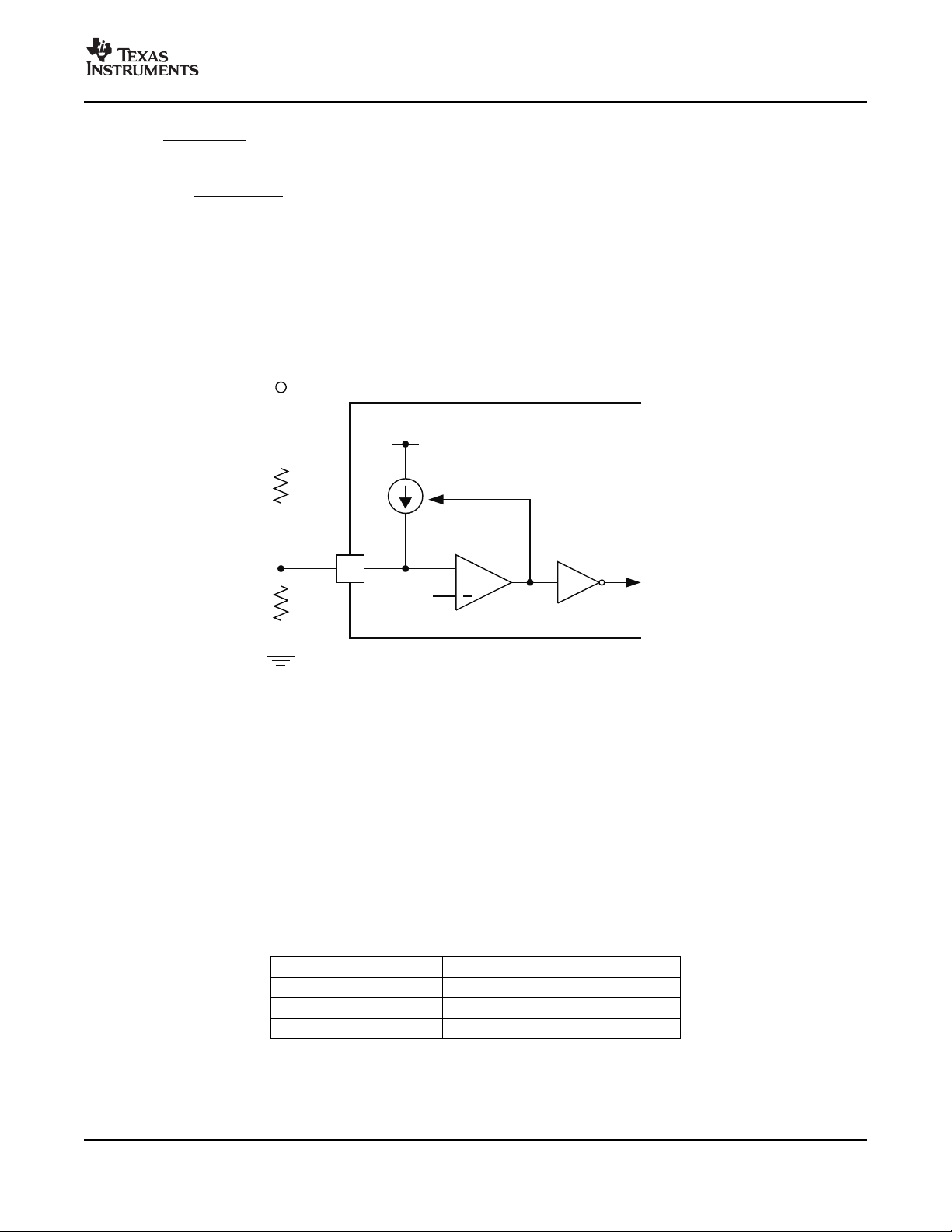
Enable Functionality
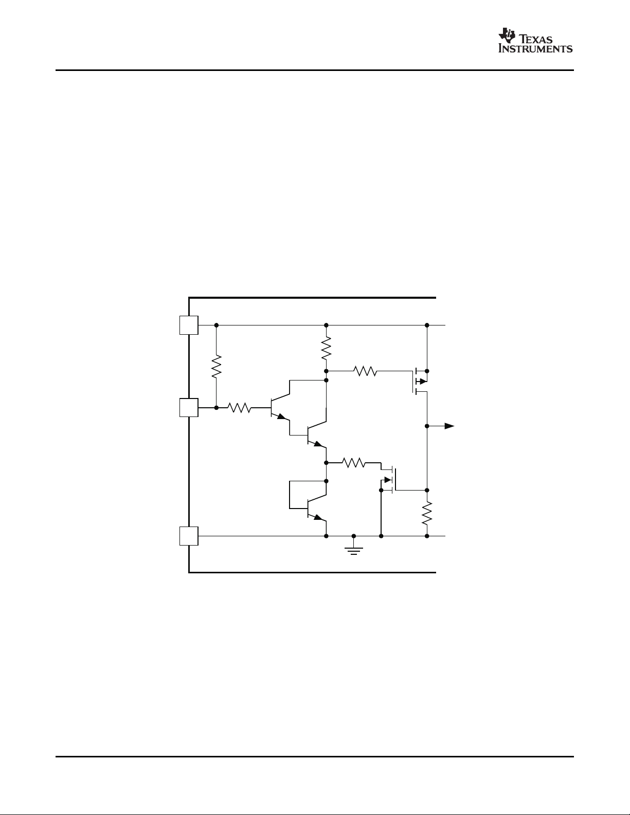
The TPS40195 has a dedicated device enable (EN) pin. This simplifies user level interface design since no
multiplexed functions exist. Another benefit is a true low power shutdown mode of operation. When the EN pin is
pulled to GND, all unnecessary functions inside the IC, including the BP regulator, are turned off and the
TPS40195 consumes a typical 165- μ A of current. A functionally equivalent circuit to the enable circuitry on the
TPS40195 is shown in Figure 16 .
If the EN pin is left floating, the chip starts automatically. The pin must be pulled to less than 600 mV for the
TPS40195 to be in shutdown mode. Note that the EN pin is relatively high impedance. In some situations, there
could be enough noise nearby to cause the EN pin to swing below the 600 mV threshold and give erroneous
shutdown commands to the rest of the device. There are two solutions to this problem should it arise.
Figure 16. TPS40195 EN Pin Internal Circuitry
1. Place a capacitor from EN to GND. A side effect of this is to delay the start of the converter while the
capacitor charges past the enable threshold
2. Place a resistor from VDD to EN. This causes more current to flow in the shutdown mode, but does not
delay converter startup. If a resistor is used, the total current into the EN pin should be limited to no more
than 500 μ A.
12
Submit Documentation Feedback
Page 13
www.ti.com
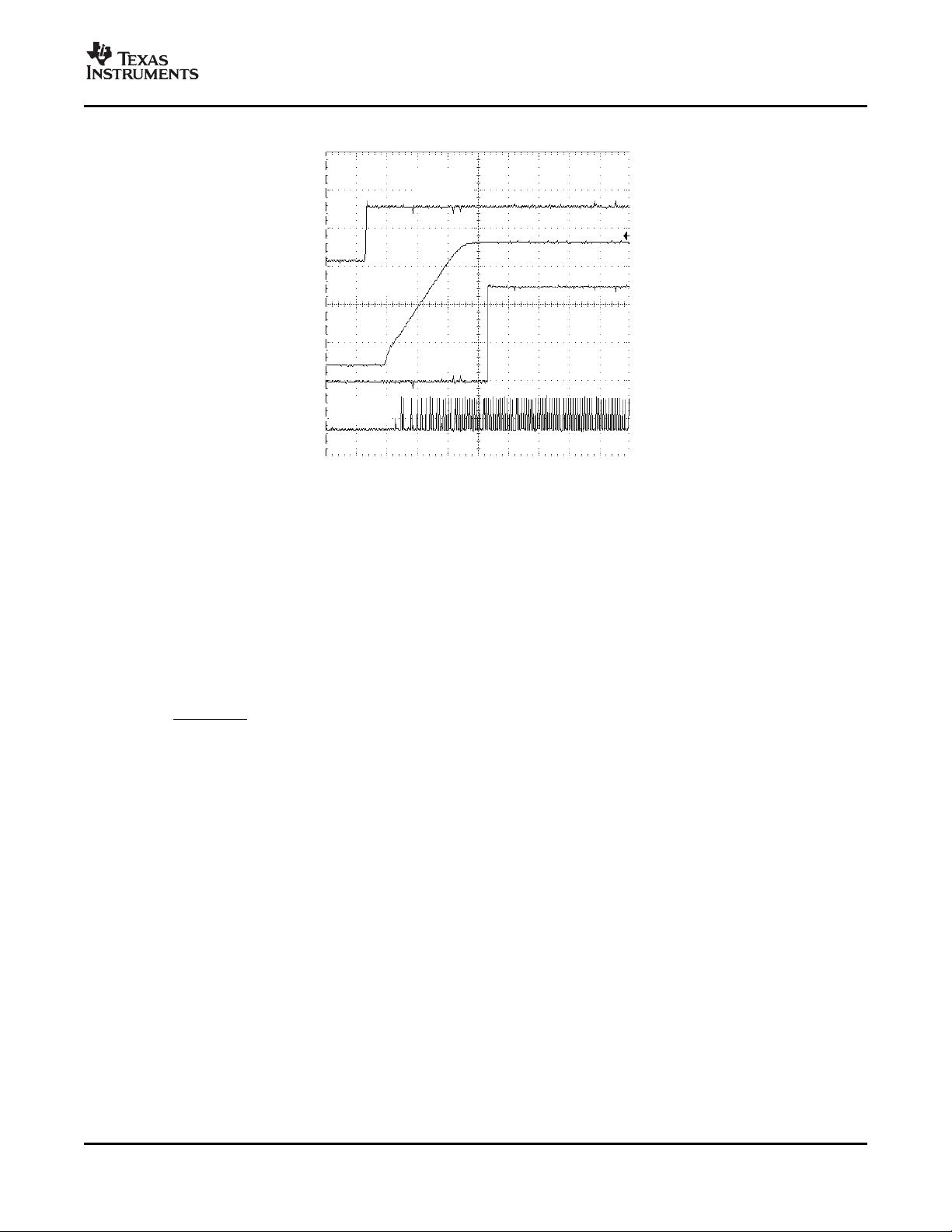
T-Time-500 ms/div
HDRV
(2V/div)
PGOOD
(2V/div)
VOUT
(1V/div)
EN
(1V/div)
( )
f
4
SW
RT
2.5 10
R
´
=
APPLICATION INFORMATION (continued)
Figure 17. TPS40195 EN Pin Startup
TPS40195
SLUS720A – FEBRUARY 2007 – REVISED JULY 2007
Voltage Reference
The band gap cell is designed with a trimmed 0.591-V output. The 0.5% tolerance on the reference voltage
allows the user to design a very accurate power supply.
Oscillator and Synchronization
The TPS40195 has a programmable switching frequency of 100 kHz to 600 kHz using a resistor connected from
the RT pin to GND. The relationship between switching frequency and the resistor from RT to GND is given in
Equation 1 .
where
• fSWis the switching frequency in kHz
• R
When the oscillator is programmed using this method, the SYNC pin is configured as an input. The device may
be synchronized to a higher frequency than the free running frequency by applying a pulse train to the SYNC
pin. For best results, limit the frequency of the pulse train applied to SYNC to 20% more than the free running
frequency. The TPS40195 will synchronize to the falling edge of the pulse train applied to the SYNC pin.
is the resistor connected from RT to GND in k Ω
RT
(1)
Submit Documentation Feedback
13
Page 14

www.ti.com
ExternalSYNC
(5V/div)
SW
(2V/div)
LDRV
(5V/div)
T-Time-1 ms/div
T-Time-1 ms/div
SW Master
(10V/div)
SW Slave
(10V/div)
SYNC
Out-of-Phase
fromMaster
TPS40195
SLUS720A – FEBRUARY 2007 – REVISED JULY 2007
APPLICATION INFORMATION (continued)
The SYNC pin can also function as an output. To get this functionality, the RT pin must be connected to either
GND or to BP. When this is done the oscillator will run at either 250 kHz or 500 kHz. SYNC can then be
connected to other TPS40195 controllers (with their SYNC pins configured as an input) and the two or more
controllers will synchronize to the same switching frequency. The output waveform on SYNC will be
approximately a 50% duty cycle pulse train. The pull up is relatively weak, but the pull down is strong to insure
that a good clean signal is presented to any devices that are to be synchronized. A summary is shown in
Table 1 .
Table 1. R
RTConnection SYNC Pin Function Switching Frequency
Resistor to GND Input See Equation 1
GND Output 250 kHz
BP Output 500 kHz
Connection and SYNC Pin Function
T
Using the TPS40195 with its RT pin connected to BP or to GND as a master clock source for another TPS40195
with a resistor connected from its RT pin to GND will result in the two controllers operating at the same
frequency but 180 ° out of phase.
Figure 18. TPS40195 Synchronized to External SYNC Pin Figure 19. TPS40195 SYNC Pin Master/Slave
Pulse (Negative Edge Triggered) Configuration. 180 ° Out-of-Phase Operation
Undervoltage Lockout (UVLO)
There are two separate UVLO circuits in the TPS40195. Both must be satisfied before the controller starts. One
circuit detects the BP voltage and the other circuit detects voltage on the UVLO pin. The voltage on the BP pin
(V
) must be above 4.3 V in order for the device to start up.
BP
The UVLO pin is generally used to provide a higher UVLO voltage than that which the BP UVLO circuit provides.
This level is programmed using a resistor divider from V
TPS40195. Hysteresis is provided by a 5.2- μ A current source that is turned on when the UVLO pin reaches the
1.26 V turn on threshold. The turn on level is determined by the divider ratio, and the hysteresis level is
determined by the divider equivalent impedance.
To determine the resistor values for the UVLO circuit, a turn on voltage and turn off voltage must be known.
Once these are known the resistors can be calculated in Equation 2 and Equation 3 . The functional schematic is
shown in Figure 20 .
14
Submit Documentation Feedback
to GND with the tap connected to the UVLO pin of the
IN
Page 15
www.ti.com
ON OFF
UVLO
V V
R1
I
-
=
UVL O
ON UV LO
V
R2 R1
V V
= ´
-
5
R1
R2
V
IN
+
BP
UVLO
1.26 V
I
UVLO
5.2 mA (typ)
UDG-07002
TPS40195
SLUS720A – FEBRUARY 2007 – REVISED JULY 2007
(2)
(3)
where
• V
• V
• I
• V
is the desired turn on voltage of the converter
ON
is the desired turn off voltage for the converter, must be less than V
OFF
is the hysteresis current generated by the device, 5.2 μ A (typ)
UVLO
is the UVLO pin threshold voltage, 1.26 V (typ)
UVLO
ON
Figure 20. Undervoltage Lockout
Soft Start
The TPS40195 uses a digital closed loop soft start system. The soft start ramp is generated internally by a
counter and digital-to-analog converter (DAC) that ramps up the effective reference voltage to the error amplifier.
The DAC supplies a voltage to the error amp that is used as the reference until that supplied voltage becomes
greater than the 591-mV reference voltage. At that point soft-start is complete and the 591-mV reference
controls the output voltage. The ramp rate is dependent on the oscillator frequency as each step in the DAC
takes one clock cycle from the oscillator. The user can choose from three ramp rates, or DAC counter widths
depending on viewpoint, for any given switching frequency by connecting the SS_SEL pin to GND, BP pin or
letting the pin float. The possibilities are summarized in Table 2 .
Table 2. Soft Start Clock Cycles
SS_SEL Connection Clock Cycles in 1-V Ramp (N
GND 2048
Floating 1024
BP 512
)
DAC
Submit Documentation Feedback
15
Page 16

www.ti.com
f
DAC
SS
SW
N
t 0.591= ´
7
ILIM
I
ILIM
9 mA
BP
R
R
+
R
ILIM
15
SW
+
t
BLNK
+
+
550 mV
VDD
LDRV On
t
BLNK
HDRV On
SQ
Q R
CLK
UP/DN
3-Bit Counter
Q0
Q1
Q2
Fault
VDD
HDRV
LDRV
UDG-07001
( )
( ) ( ) ( )
( )( )
ILIM min ILIM min ILIMOFST min
SCP min
DS on max
I R V
I
R
´ +
=
TPS40195
SLUS720A – FEBRUARY 2007 – REVISED JULY 2007
The ramp output from the soft start DAC is 1 V in amplitude. Since the soft start is closed loop and reference
voltage of the device is actually 591 mV, the actual ramp time is less than the time it takes for the SS ramp to
finish and reach 1 V. The actual soft-start time is the amount of time that it takes for the internal soft-start ramp
to reach the 591-mV reference level. The soft-start time can be found using Equation 4 .
where
• N
• fSWis the switching frequency in Hz
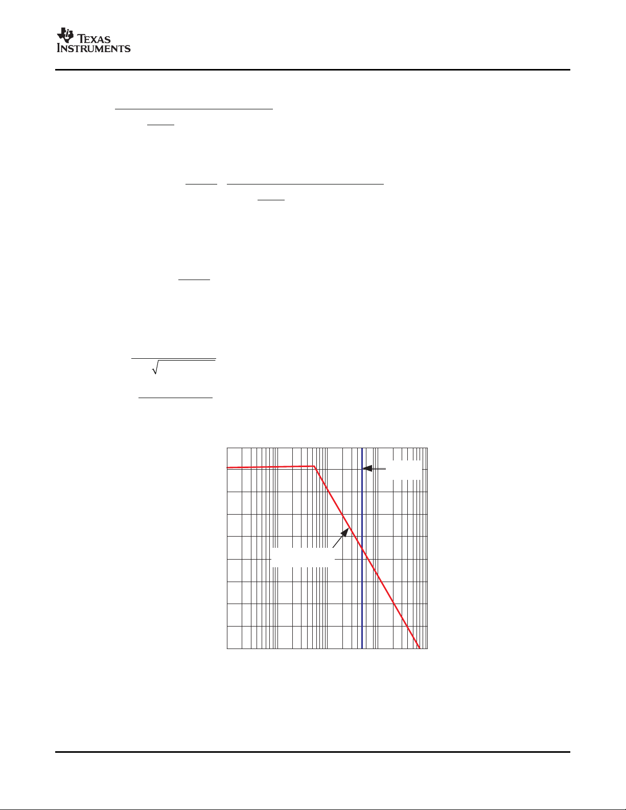
Selecting the Short Circuit Threshold
A short circuit in the TPS40195 is detected by sensing a voltage drop across the low-side FET when it is on, and
across the high-side FET when it is on. If the voltage drop across either FET exceeds the short circuit threshold
in any given switching cycle, a counter increments one count. If the voltage across the high-side FET was higher
that the short circuit threshold, that FET is turned off early. If the voltage drop across either FET does not
exceed the short circuit threshold during a cycle, the counter is decremented for that cycle. If the counter fills up
(a count of 7) a fault condition is declared and the drivers turn off both MOSFETs. After a timeout of
approximately 40 ms, the controller attempts to restart. If a short circuit remains present at the output, the
current quickly ramps up to the short circuit threshold and another fault condition is declared and the process of
waiting for the 40 ms and attempting to restart repeats.
The current limit threshold for the low-side FET is programmable by the user. To set the threshold a resistor is
connected from the ILIM pin to GND. A current source inside the IC connected to the ILIM pin and this resistor
set a voltage that is the threshold used for the overcurrent detection threshold. The low side threshold will
increase as the low side on time decreases due to blanking time and comparator response time. See Figure 5
for changes in the threshold as the low-side FET conduction time decreases. Refer to Figure 21 for details on
the functional equivalent schematic.
is the number of 1-V DAC ramp cycles from Table 2
DAC
(4)
16
Figure 21. Overcurrent
Submit Documentation Feedback
(5)
Page 17

www.ti.com
( )
( ) ( ) ( )
( )
ILIM max ILIM max ILIMOFST max
SCP max
DS(on) min
I R V
I
R
´ +
=
( )
( )
( )
ILIMH min
OUT max
DS(on) max
V
I
R
=
f
DAC
OFF
SC
7 Nt´
=
TPS40195
SLUS720A – FEBRUARY 2007 – REVISED JULY 2007
where
• I
• I
• R
• V
• R
The short circuit protection threshold for the high-side MOSFET is fixed at 550-mV typical, 400-mV minimum
with a 4000 ppm/ ° C temperature coefficient to help compensate for changes in the high side FET channel
resistance as temperature increases. This threshold is in place to provide a maximum current output in the case
of a fault. The maximum amount of current that can be sourced from a converter can be found by Equation 7 .
where
• I
• V
• R
If the required current from the converter is greater than the calculated I
MOSFET must be chosen.
The length of time between restart attmepts after an output fault can be found from Equation 8 .
is the short circuit current
S.P.
is ILIM pin bias current, 9.0 μ A (typ)
ILIM
is the resistance connected from ILIM to GND
ILIM
is the offset voltage of the low side current sense comparator, ± 20 mV
ILIMOFST
is the channel resistance of the low-side MOSFET
DS(on)
OUT(max)
is the maximum current that the converter is specified to source
ILIMH(min)
DS(on)max
is the short circuit threshold for the high-side MOSFET (400 mV)
is the maximum resistance of the high-side MOSFET
OUT(max)
, a lower resistance high-side
(6)
(7)
where
• N
• fSWis the switching frequency in Hz
is the number of 1-V DAC ramp cycles from Table 2 .
DAC
5-V Regulator
This device has an on board 5-V regulator that allows the parts to operate from a single voltage feed. No
separate 5-V feed to the part is required. This regulator requires a minimum of 1 μ F of capacitance on the BP
pin for stability. A ceramic capacitor is suggested for this purpose. Noise performance can be improved by
increasing this capacitance to 4.7 μ F when driving FETs with more than 25nC gate charge requirements.
This regulator can also be used to supply power to nearby circuitry, eliminating the need for a separate LDO in
some cases. If this pin is used for external loads, be aware that this is the power supply for the internals of the
TPS40195. While efforts have been made to reduce sensitivity, any noise induced on this line has an adverse
effect on the overall performance of the internal circuitry and shows up as increased pulse jitter, or skewed
reference voltage. Note that when the EN pin is pulled low, the BP regulator will be turned off and not available
to supply power to external loads.
The amount of power available from this pin varies with the size of the power MOSFETs that the drivers must
operate. Larger MOSFETs require more gate drive current and reduces the amount of power available on this
pin for other tasks.
(8)
Submit Documentation Feedback
17
Page 18

www.ti.com
TPS40195
SLUS720A – FEBRUARY 2007 – REVISED JULY 2007
Pre-Bias Startup
The TPS40195 contains a unique circuit to prevent current from being pulled from the output during startup in
the condition the output is pre-biased. When the soft-start commands a voltage higher than the pre-bias level
(internal soft-start becomes greater than feedback voltage [V
rectification by starting the first LDRV pulses with a narrow on-time. It then increments that on-time on a
cycle-by-cycle basis until it coincides with the time dictated by (1-D), where D is the duty cycle of the converter.
This scheme prevents the initial sinking of the pre-bias output, and ensures that the out voltage (V
ramps up smoothly into regulation and the control loop is given time to transition from pre-biased startup to
normal mode operation with minimal disturbance to the output voltage. The amount of time from the start of
switching until the low-side MOSFET is turned on for the full 1-D interval is defined by 32 clock cycles.
Drivers
The drivers for the external HDRV and LDRV MOSFETs are capable of driving a gate-to-source voltage of 5 V.
The LDRV driver switches between VDD and GND, while HDRV driver is referenced to SW and switches
between BOOT and SW. The drivers have non-overlapping timing that is governed by an adaptive delay circuit
to minimize body diode conduction in the synchronous rectifier. The drivers are capable of driving MOSFETS
that are appropriate for a 15-A converter if power dissipation requirements are met. See Package Dissipation
Ratings Table.
Power Good
The TPS40195 provides an indication that output power is good for the converter. This is an open drain signal
and pulls low when any condition exists that would indicate that the output of the supply might be out of
regulation. These conditions include:
• V
• soft-start is active
• a undervoltage condition exists for the device
• a short circuit condition has been detected
• die temperature is over (150 ° C)
FB
> ± 10% from nominal
]), the controller slowly activates synchronous
FB
) starts and
OUT
NOTE
When there is no power to the device, PGOOD is not able to pull close to GND if an
auxiliary supply is used for the power good indication. In this case, a built in resistor
connected from drain to gate on the PGOOD pull down device makes the PGOOD
pin look approximately like a diode to GND.
Thermal Shutdown
Thermal shutdown If the junction temperature of the device reaches the thermal shutdown limit of 150 ° C, the
PWM and the oscillator is turned off and HDRV and LDRV are driven low, turning off both FETs. When the
junction cools to the required level (130 ° C nominal), the PWM initiates soft start as during a normal power up
cycle.
18
Submit Documentation Feedback
Page 19

www.ti.com
1
2
3
4
16
15
14
13
HDRV
SW
BOOT
LDRV
EN
FB
COMP
VDD
TPS40195
5
6
7 8
UVLO
RT
ILIM
GND
12
11
10 9
BP
SS_SEL
PGOOD
SYNC
PWR GND
V
IN
V
OUT
Output Current Loop
V
OUT
to GND
Input Current Loop
V
IN
to GND
UDG-07004
Signal Ground
Low-Side
Drive Current
C
IN
High-Side
Drive Current
TPS40195
SLUS720A – FEBRUARY 2007 – REVISED JULY 2007
Layout Suggestions
Figure 22. Layout Suggestion
• Keep the input switching current loop as small as possible.
• Place the input capacitor (C
) close to the top switching FET The output loop current loop should also be
IN
kept as small as possible.
• Keep the SW node as physically small as possible to minimize parasitic capacitance and to minimize
radiated emissions Kelvin connections should be brought from the output to the feedback pin (FB) of the
device.
• Keep analog and non-switching components away from switching components.
• The gate drive trace should be as close to the power FET’s gate as possible.
• Make a single point connection from the signal ground to power ground.
• Do not allow switching current to flow under the device.
Submit Documentation Feedback
19
Page 20

www.ti.com
Input capacitors near Drain
of top FET
Small switch node area
Analog components away
from Power Switching
elements
Kelvin Feed back
connection
TPS40195
SLUS720A – FEBRUARY 2007 – REVISED JULY 2007
Figure 23. Board Layout
20
Submit Documentation Feedback
Page 21

www.ti.com
TPS40195
SLUS720A – FEBRUARY 2007 – REVISED JULY 2007
DESIGN EXAMPLES
Design Example 1
Table 3. Design Example Electrical Specifications
PARAMETER TEST CONDITIONS MIN TYP MAX UNIT
INPUT
V
IN
I
IN
VIN_
UVLO_OFF
VIN_UVLO
_ON
OUTPUT
V
OUT
V
OUT(ripple)
I
OUT
I
OCP
Δ I Transient response load step 10 A ≤ I
SYSTEM
f
SW
η
PK
η Efficiency at full load VIN= 12 V, I
T
OP
MECHANICAL
W Width 1.6
L Length 3.5 in
h Height 0.26
Input voltage 10.8 12.0 13.2 V
Input current
Undervoltage lockout turn off threshold 0 A ≤ I
Undervoltage lockout turn on threshold 0 A ≤ I
VIN= 12 V, I
No load, VIN= 12 V, I
OUT
OUT
Input voltage range VIN= 12 V, I
= 10 A 1.7 1.8 A
OUT
= 0 A 5 mA
OUT
≤ 10 A 5.4 6.0 6.6
≤ 10 A 6.6 7.0 7.6
= 5 1.75 1.80 1.85 V
OUT
Line regulation 10.8 ≤ VIN≤ 13.2 V 0.5%
Load regulation 0 A ≤ I
Output voltage ripple VIN= 12 V, I
≤ 10 A 0.5%
OUT
= 10 A 100 mV
OUT
Output current 10.8 ≤ VIN≤ 13.2 V 0 5 10
Output overcurrent inception point VIN= 12 V, V
OUT(max)
OUT
≤ 0.2 × ( I
= (V
- 5) 14 20 43
OUT
) 8 A
OUT(max)
Transient response load slew rate 5 A/ μ s
Transient response overshoot 200 mV
Transient response settling time 1 ms
Switching frequency 240 300 360 kHz
Peak efficiency VIN= 12 V, 0 A ≤ I
OUT
Operating temperature range 10.8 ≤ VIN≤ 13.2 V, 0 A ≤ I
≤ 10 A 90%
OUT
= 10 A 87%
≤ 10 A -40 25 85 ° C
OUT
V
P-P
A
Submit Documentation Feedback
21
Page 22

www.ti.com
f
IN(max) OUT
OUT
OUT
IN(max) SW RIPPLE
(V - V )
V
1.8 V (13.2 V -1.8 V)
L 2.59 H
V I 13.2 V 300kHz 2.0
= ´ = ´ = m
´ ´
f
IN(max) OUT
OUT
RIPPLE
IN(max) SW OUT
(V V )
V
1.83 V (13.2V 1.83 V)
I 2.10 A
V L 13.2 V 300 kHz 2.5 H
-
-
= ´ = ´ =
´ ´ m
( )
( )
( )
( )
2 2
2
2
RIPPLE
LOUT _RMS OUT
I 2.10
I I 10 10.02 A
12 12
= + = + =
RIPPLE
PK OUT
I
2.10
I I 10 11.05 A
2 2
= + = + =
TPS40195
SLUS720A – FEBRUARY 2007 – REVISED JULY 2007
Schematic
This section discusses basic buck converter design. Designers already familiar with the design of buck
converters can skip to the next section Component Selection of this design example.
Figure 24. TPS40195 Design Example Schematic
Output Inductor, L
Equation 9 can be used to calculate L
OUT
.
OUT
where
• I
= the allowable ripple current in the inductor, 20% of maximum I
RIPPLE
For this design a 2.5- μ H inductor from Coilcraft is used. I
inductor value to give a new estimate of I
With this I
value, the RMS and peak current flowing in L
RIPPLE
of 2.1 A .
RIPPLE
OUT
is recalculated using Equation 10 and a 2.5- μ H
RIPPLE
can be calculated.
OUT
(9)
(10)
(11)
(12)
22
Submit Documentation Feedback
Page 23

www.ti.com
( )
( )
( )
( )
2
2
OUT STEP
OUT
UNDER MAX IN(min) OUT
L I
2.5 H 8
C 71.68 F
2 200mV 90% 10.8 V 1.8 V
2 V D V V
´
m ´
= = = m
´ ´ ´ -
´ ´ ´ -
( )
2
2
OUT STEP
OUT
OVER OUT
L I
2.5 H 8
C 222.2 F
2 V V 2 200 mV 1.8 V
´
m ´
= = = m
´ ´ ´ ´
RIPPLE
RIPPLE
V
100mV
ESR 47 m
I 2.1A
= = = W
( )
2
2 2
RIPPLE
OUT OUT OUT OUT
CAP(RMS) OUT OUT OUT
IN IN IN IN
I
V V V V
I I I I 1
V 12 V V V
é ù
æ ö æ ö æ ö
ê ú
= - ´ + ´ + ´ ´ -
ç ÷ ç ÷ ç ÷
ê ú
è ø è ø è ø
ë û
( )
( )
2
2
RIPPLE
OUT
QSW(rms) OUT(max)
IN(min)
I
V
I I
V 12
æ ö
ç ÷
= ´ +
ç ÷
è ø
f
GATE g(TOT) g SW
P Q V= ´ ´
GATESWCONQSW
PPPP ++=
TPS40195
SLUS720A – FEBRUARY 2007 – REVISED JULY 2007
Output Capacitor, C
OUT
The capacitance value is selected to be greater than the largest value calculated from Equation 13 and
Equation 14 .
From Equation 13 , Equation 14 and Equation 15 , the capacitance for C
should be greater than 223 μ F and
OUT
its ESR should be less than 47 m Ω . Three 100- μ F, 6.3-V, X5R ceramic capacitors are chosen. Each capacitor
has an ESR of 5 m Ω .
Input Capacitor, C
IN
The input capacitor is selected to handle the ripple current of the buck stage. A relatively large capacitance is
used to keep the ripple voltage on the supply line low. This is especially important were the supply line has a
high impedance. It is recommended that the supply line impedance be kept low. The input capacitor RMS
current can be calculated using Equation 16 .
(13)
(14)
(15)
The RMS current in the input capacitor is 3.56 A. Two 22- μ F, size 1206 capacitors using X7R material has a
typical dissipation factor of 5%. For a 22- μ F capacitor at 300 kHz the ESR is approximately 5 m Ω . Two of these
capacitors are used in parallel. The power dissipation in each capacitor is less than 16 mW. A 470- μ F, 25-V
electrolytic is added to maintain the voltage on the input rail.
Switching MOSFET, Q
SW
The following key parameters must be met by the selected MOSFET.
• Drain-to-source voltage, V
switching node. For this design a V
, must be able to withstand the input voltage plus spikes that may be on the
DS
rating of between 25 V and 30 V is recommended.
DS
For this design IDDshould be greater than 4.1 A
• Gate source voltage, V
, must be able to withstand the gate voltage from the control device. For the
gs
TPS40195 this is 5 V.
Target efficiency for this design is 90%. Based on 1.8-V output and 10-A operating current this equates to a
power loss in the module of 1.8 W. The design allocates this power budget equally between the two power
FETS and the inductor The equations below are used to calculate the power loss, P
, in the switching
QSW
MOSFET.
(16)
(17)
(18)
Submit Documentation Feedback
(19)
23
Page 24

www.ti.com
( )
( )
( )
2
2
2
RIPPLE
OUT
CON DS(on) QSW(rms) DS(on) OUT
IN
I
V
P R I R I
V 12
æ ö
ç ÷
= ´ = ´ ´ +
ç ÷
è ø
( )
f
RIPPLE
OUT g s1 gd
SW IN S
g
I
I Q Q
2
P V
I
é ù
æ ö
+ ´ +
ê ú
ç ÷
è ø
ê ú
= ´ ´
ê ú
ê ú
ë û
QSR CON BD GATE
P P P P= + +
( )
( )
( )
2
2
2
RIPPLE
OUT
CON DS(on) QSW(rms) DS(on) OUT
IN
I
V
P R I R I
V 12
æ ö
ç ÷
= ´ = ´ ´ +
ç ÷
è ø
f
GATE g(TOT) g SW
P Q V= ´ ´
( )
f
BD f OUT 1 2 S
P V I t t= ´ ´ + ´
TPS40195
SLUS720A – FEBRUARY 2007 – REVISED JULY 2007
where
• P
• P
• P
• Q
• Q
• Igis gate drive current
• Q
• Vgis gate voltage
Equation 22 and Equation 23 describe the preliminary values for R
due to Q
OSS
added. The switching MOSFET for this design should have an R
Q
should be approximately 14.8 nC. . The Vishay SI7860ADP was selected for this design. This device has
gs1
an R
of 9 m Ω and a (Q
DS(on)
losses are 0.297 W. This gives a total estimated power loss of 0.432 W versus 0.6 W for our initial boundary
condition. Note this does not include gate losses of approximately 10 mW.
is conduction losses
CON
is switching losses
SW
is gate drive losses
GATE
is drain source charge or miller charge
gd
is gate source post threshold charge
gs1
is total gate charge from 0 V to the gate voltage
g(TOT)
and (Q
DS(on)
+ Q
gs1
). Note output losses
gd
and gate losses have been ignored here. Once a MOSFET is selected these parameters can be
of less than 20 m Ω . The sum of Q
DS (on)
+Q
gs1
) of 13 nC. The estimated conduction losses are 0.135 W and the switching
gd
(20)
(21)
and
gd
Rectifier MOSFET, Q
SR
Similar criteria as used above apply to the rectifier MOSFET. One significant difference however, is that the
rectifier MOSFET switches with nearly zero voltage across its drain and source so its switching losses are nearly
zero. There are losses from the source to drain body diode that occur as it conducts during the delay before the
FET turns on. The equations used to calculate the losses in the rectifier MOSFET are shown below.
where
• P
• t1is the body diode conduction prior to turn-on of channel (57nS)
• t2is the body diode conduction after turn-off of channel (14nS)
• Vfis the body diode forward voltage
is the body diode loss
BD
Estimating the body diode losses based on a forward voltage of 1.0 V yields 0.162 W. The gate losses are
unknown at this time so assume 0.1 W gate losses. This leaves 0.338 W for conduction losses. Using this figure
a target R
of 4.0 m Ω was calculated. The SI7886ADP has an R
DS(on)
maximum of 4.8 m Ω and was used for
DS(on)
this design.
(22)
(23)
(24)
24
Submit Documentation Feedback
Page 25

www.ti.com
( ) ( )
f
7 7
T
S
2.5 10 2.5 10
R 83.3k
300
´ ´
= = = W
( )
ON OFF
UVLO1
6
UVLO
V V
7 6
R 192.3k
I
5.2 10
-
-
-
= = = W
´
( )
UVLO
UVLO2 UVLO1
ON UVLO
V
1.26
R R 192.3k 42.2k
7 1.26
V V
= ´ = W ´ = W
-
-
START OUT OUT
t 2 L C³ p´ ´
( ) ( )
6 6
START
t 6.28 2.5 10 300 10 0.172ms
- -
³ ´ ´ ´ ´ =
f
DAC
SS
SW
N
1024
t 0.591 0.591 2.0 m s
300
= ´ = ´ =
TPS40195
SLUS720A – FEBRUARY 2007 – REVISED JULY 2007
Using the parameters from its data sheet the actual expected power losses were calculated. Conduction loss is
0.394 W, body diode loss is 0.210 W and the gate loss was 0.063 W. This totals 0.667 W associated with the
rectifier MOSFET.
The ratio between C
reduce the risk of dv/dt induced turn on of the rectifier MOSFET. If this is likely to be a problem a small resistor
may be added in series with the boost capacitor, C
increased switching losses in that device.
Component Selection for the TPS40195
and C
gs
should be greater than one. The Si7886 capacitor meets this criterion and helps
gd
. to slow the turn on speed of Q
BOOST
at the expense of
SW
Timing Resistor, R
T
The timing resistor is calculated using the following equation.
A standard value resistor of 82.5 k Ω is used.
Setting UVLO
The equations below are used to set the UVLO voltages.
The UVLO threshold voltage ( V
of 6 V. This sets R
to 191 k Ω , the nearest standard value. The second resistor R
UVLO1
) is 1.26 V. The module has a turn on voltage of 7 V and a turn off voltage
UVLO
UVLO2
is 42.2 k Ω .
Setting the Soft-Start Time
The selection of the soft start time should be greater than the time constant of the output filter, L
This time is given in Equation 28 and Equation 29 .
(25)
(26)
(27)
and C
OUT
.
OUT
The soft-start time is determined using Equation 30 . The TPS40195 uses a counter operating at the clock
frequency that increments an internal DAC until it reaches the turn on threshold voltage of 0.591 V. The number
of counts required to reach this threshold is determined by one of three settings on the SS pin. In this case, the
pin is floating (with a small bypass capacitor) which sets the clock count (N
2.0 ms
Submit Documentation Feedback
) to 1024 and the soft-start time is
DAC
(28)
(29)
(30)
25
Page 26

www.ti.com
( )
( )
6
OUT OUT
SCP PK
3
STA RT
300 10 1.8
C V
I I 11.05 11.32 A
t
2 10
-
-
´ ´
´
³ + = + =
´
( )
( ) ( ) ( )
( )
( )
3
DS on (max) SCP min ILIMOFSET min
ILIM min
6
LIM(min)
R I V
(4.88 10 14) 20 mV
R 12.6k
I
7.0 10
-
-
´ -
´ ´ +
= = = W
´
( )
( ) ( ) ( )
( )( )
ILIM min ILIM min ILIMOFST min
SCP min
DS on max
I R V
I
R
´ +
=
( )
( ) ( ) ( )
( )
ILIM max ILIM max ILIMOFST max
SCP max
DS(on) min
I R V
I
R
´ +
=
( )
g TOT
BOOST
BOOST
Q
C
ΔV
>
IN
PW M
RAM P
V
K
V
@
TPS40195
SLUS720A – FEBRUARY 2007 – REVISED JULY 2007
Short Circuit Protection, R
Short circuit protection is programmed using the R
of the switching MOSFET and the required short circuit current trip point, I
ILIM
resistor. Selection of this resistor depends on the R
ILIM
. The minimum I
SCP
must exceed
SCP
the sum of the output current, the peak ripple current, and the output capacitor charging current during start up.
Equation 30 gives this minimum.
The minimum short circuit current trip point for this design is set to 14 A. Equation 32 is then used to calculate
the minimum R
R
is calculated to be 12.6 k Ω . The closest standard value of 12.7 k Ω is used. The minimum and maximum
ILIM
value.
ILIM
short circuit current can be calculated using Equation 33 and Equation 34 .
The minimum I
is 14 A and the maximum is 46 A.
SCP
DS(on)
(31)
(32)
(33)
(34)
Voltage Decoupling Capacitors, C
BP
, and C
VDD
Two pins on the TPS40195 have DC voltages. It is recommended to add small decoupling capacitors to these
pins. Below are the recommended values.
• C
• C
Boost Voltage, C
BP
VDD
= 4.7 μ F
= 0.1 μ F
and D
BOOST
BOOST (
optional)
Selection of the boost capacitor is based on the total gate charge of the switching MOSFET and the allowable
ripple on the boost voltage, V
equation (26) the minimum value for C
The total gate charge of the switching MOSFET is 13.3 nC. A minimum C
. A ripple of 0.2 V is assumed for this design. Using these two parameter and
BOOST
can be calculated.
BOOST
of 0.066- μ F is required. A 0.1- μ F
BOOST
capacitor was chosen. This capacitor must be able to withstand the maximum input voltage plus the maximum
voltage on BP. This is 16 V plus 5.4 V which is 21.4 V. A 50-V capacitor is used.
To reduce losses in the TPS40195 and to increase the available gate voltage for the switching MOSFET an
external diode can be added between the BP pin and the BOOST pin of the device. A small signal schottky
should be used here, such as the BAT54.
Closing the Feedback Loop R
, R
, R
Z1
P1
, R
PZ2
, R
SET1
, C
, C
SET2
Z2
AND C
P2
PZ1
A graphical method is used to select the compensation components. This is a standard feedforward buck
converter. Its PWM gain is given by the following equation.
(35)
26
Submit Documentation Feedback
(36)
Page 27
www.ti.com
( )
( )
OUT
LC
2
OUT
OUT OUT
OUT
1 s ESR C
K
L
1 s s L C
R
+ ´ ´
=
æ ö
+ ´ + ´ ´
ç ÷
è ø
( )
( )
OUT
IN
e PWM LC
2
RAMP
OUT
OUT OUT
OUT
1 s ESR C
V
G (s) K K
V
L
1 s s L C
R
+ ´ ´
= ´ = ´
æ ö
+ ´ + ´ ´
ç ÷
è ø
IN
RAMP
V
DCgain 20 LOG 20 LOG(12) 21.6 dB
V
æ ö
= ´ = ´ =
ç ÷
è ø
f
LC_Pole
OUT OUT
1
5.8kHz
2 L C
= =
p´ ´
ESR_Zero
OUT
1
f 990 k Hz
2 ESR C
= =
p´ ´
−60
−30
−10
0
10
30
−50
100 1 k 10 k 1 M100 k
−40
−20
20
Double
Pole
L−C Slope
40 dB/decade
f − Frequency − Hz
Gain − dB
TPS40195
SLUS720A – FEBRUARY 2007 – REVISED JULY 2007
The gain of the output LC filter is given in Equation 37 .
The equation for the PWM and LC gain is:
To plot this on a Bode plot the DC gain must be expressed in dB. The DC gain is equal to K
in dB we take its LOG and multiple by 20. For this converter the DC gain is:
Also the pole and zero frequencies should be calculated. A double pole is associated with the LC and a zero is
associated with the ESR of the output capacitance. The frequency at where these occur can be calculated using
Equation 40 .
. To express this
PWM
(37)
(38)
(39)
A Bode plot of the PWM and LC filter is shown in Figure 25 .
Figure 25. PWM and L-C Filter Gain
A Type-III compensation network, shown in Figure 26 , is used for this design. A typical bode plot of a Type-III
compensation network is shown below in Figure 27 .
(40)
(41)
Submit Documentation Feedback
27
Page 28

www.ti.com
2
3
TPS40195
R
SET
R
PZ2
C
Z2
C
PZ
FB
COMP
R
Z1
R
P1
C
PZ
−20
100 1 k 1 M
−10
0
10
20
30
40
f − Frequency − Hz
Gain − dB
f
P2
f
P1
f
Z2
f
Z1
High−Frequency
Gain
( )
( )
REGF Z1
SET
OUT REF
V R
R
V V
´
=
-
SE T
0.591 51k
R 24.9 k
1.8 0.591
´ W
= = W
-
f
f
PZ2 Z1 P1
c PZ1
Z1 P1
C PZ1
1
R R R
2 C
Gain
1
R R
2 C
æ ö
æ ö
´ + +
ç ÷
ç ÷
ç ÷
p ´
è ø
è ø
=
æ ö
+
ç ÷
p ´
è ø
P1
P1 PZ1
1
f
2 R C
=
p´ ´
P2 Z2
P2
PZ 2 P 2 Z 2 PZ 2 P 2
C C
1
f
2 R C C 2 R C
+
= »
p´ ´ ´ p ´ ´
Z1
Z1 PZ1
1
f
2 R C
=
p´ ´
( )
Z 2
PZ 2 P 1 Z 2 PZ 2 Z 2
1 1
f
2 R R C 2 R C
= »
p ´ + ´ p ´ ´
TPS40195
SLUS720A – FEBRUARY 2007 – REVISED JULY 2007
Figure 26. Type III Compensation Schematic Figure 27. Type-III Compensation Network Typical Bode
Plot
The output voltage, the high-frequency gain and the break (pole and zero) frequencies are calculated using the
following equations.
(42)
(43)
(44)
(45)
(46)
Steps in closing the feedback loop.
1. Place one zero well below the L-C double pole at 5.8 kHz (f
2. Place the second zero near the double pole fZ2at 5.8 kHz.
3. Place one pole well above the desired cross over frequency, selected as one sixth the switching
frequency, f
28
CO1
= 50 kHz, fP1= 300 kHz
Submit Documentation Feedback
(47)
(48)
=2.1 kHz)
Z1
Page 29
www.ti.com
0
15
20
25
30
5
100 1 k 100 k10 k
10
f
SW
- Switching Frequency - kHz
Gain - dB
0
20
80
100
140
180
200
120
40
60
160
PHASE
GAIN
Phase - °
TPS40195
SLUS720A – FEBRUARY 2007 – REVISED JULY 2007
4. Place the second pole near the ESR pole of the output capacitors of 338 kHz. fP2= 338 kHz
5. The high frequency gain must be such that the over all system has 0 dB at the required crossover
frequency. This gain is -1 times the sum of the modulator gain and the gain of the output stage at the
crossover frequency of 50 kHz.
Using these values and the above equations calculate the set point and the Rs and Cs around the
compensation network using the following procedure.
1. Set R
2. Calculate R
3. Using Equation 47 and fZ1= 1.8 kHz, C
R
4. From Figure 25 , the required gain is calculated at 15.8 dB. Equation 44 sets the value for R
for R
the second zero, C
5. C
used.
= 51 k Ω
Z1
using Equation 42 . For this module R
SET
can be calculated to be 1500 pF, F
to be 363 Ω and the standard value 357 Ω is used.
P1
with value of 12.7 k Ω is used. C
PZ2
is calculated using the second pole frequency and Equation 46 , C
P2
= 1475 pF. A 2200 pF capacitor is used.
Z2
PZ1
is calculated using Equation 48 and the desired frequency for
Z2
= a standard 1% value = 24.9 k Ω .
SET
and Equation 45 yields
P1
. A resistor
PZ2
= 37 pF. A 33-pf capacitor is
P2
Figure 28. Final Bode Plot
Submit Documentation Feedback
29
Page 30
www.ti.com
+
0 2 4 6 8 10
I
OUT
- Load Current - A
3.305
3.311
3.314
3.316
3.307
3.309
3.312
3.313
3.315
3.308
3.310
3.306
V
OUT
- Output Voltage - V
13.2 V
12.0 V
10.8 V
V
IN
h - Efficiency - %
0 2 4 6 8
I
OUT
- Load Current - A
10
10.8 V
12.0 V
13.2 V
V
IN
TPS40195
SLUS720A – FEBRUARY 2007 – REVISED JULY 2007
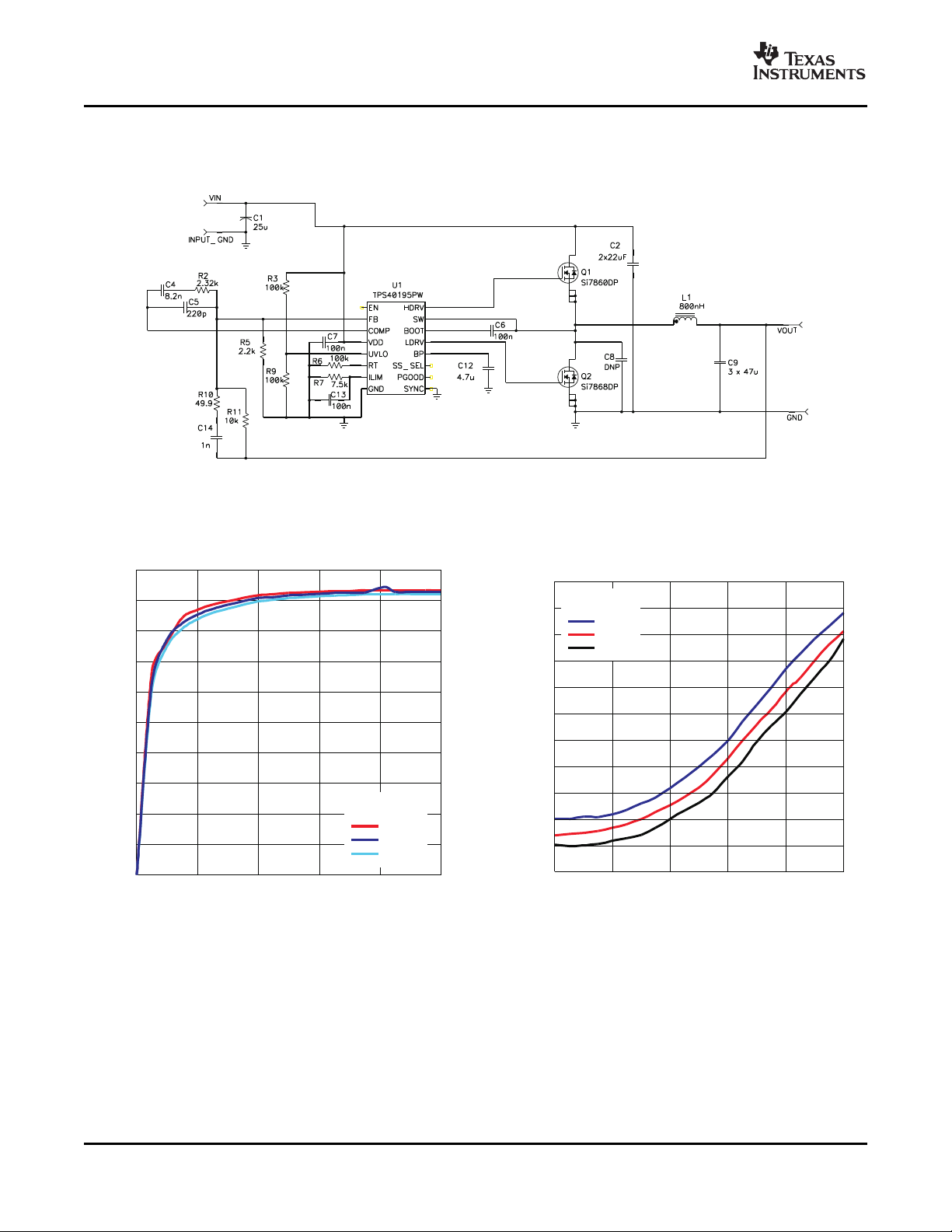
Design Example 2
This example demonstrates the performance of the TPS40195 in a design that produces 5 A of output current at
a user selectable voltage of 3.3 V. The input for this design is 12 V ± 10%.
Figure 29. Design Example 2 Schematic
EFFICIENCY OUTPUT VOLTAGE
LOAD CURRENT LOAD CURRENT
30
vs vs
Figure 30. Figure 31.
Submit Documentation Feedback
Page 31
www.ti.com
TPS40195
SLUS720A – FEBRUARY 2007 – REVISED JULY 2007
Table 4. Design Example 2 Bill of Materials
QTY RefDes Value Description Size Part Number MFR
1 C1 25 μ F Capacitor, Aluminun, 25V, SM ± 20% 0.406 in × EEVFK1E471P Panasonic
2 C2 22 μ F Capacitor, Ceramic, 16V, XR5, 20% 0603 Std Std
1 C4 8.2 nF Capacitor, Ceramic, 16V, X7R, 10% 0603 Std Std
1 C5 220 pF Capacitor, Ceramic, 16V, X7R, 10% 0603 Std Std
3 C6, C7, 100 nF Capacitor, Ceramic, 16V, X7R, 10% 0603 Std Std
C13
1 C8 1 nF Capacitor, Ceramic, 50V, X7R,10% 0805 Std Std
1 C9 47 μ F Capacitor, Ceramic, 6.3V, X5R, 20% 1210 C3225X5R0J476M TDK
1 C12 4.7 μ F Capacitor, Ceramic, 10V, X5R, 10% Std Std
1 C14 1 nF Capacitor, Ceramic, 16V, X7R, 10% 0603 Std Std
1 L1 800 nH Inductor, SMT, 31A 0.512 × 0.571 PG0077.801 Pulse
1- Q1 Si7860DP MOSFET, N-Ch, 30V, 15A, 11m Ω SOT-8 Si7860DP Vishay
1 Q2 Si7868DP MOSFET, N-Ch, 20V, 2.75 m Ω , 25 A SOT-8 Si7868DP Vishay
3 R2, R3, 2.32 k Ω Resistor, Chip, 1/16W, 5% 0603 Std Std
R6
1 R5 2.2 k Ω Resistor, Chip, 1/16W, 5% 0603 Std Std
1 R7 7.5 k Ω Resistor, Chip, 1/16W, 1% 0603 Std Std
1 R9 100 k Ω Resistor, Chip, 1/16W, 1% 0603 Std Std
1 R10 49.9 k Ω Resistor, Chip, 1/16W, 1% 0603 Std Std
1 R11 10 k Ω Resistor, Chip, 1/16W, 1% 0603 Std Std
1 U1 TPS40195PW 4.5-V to 20-V Synchronous Buck TSSOP-16 TPS40195PW TI
Controller
0.457 in
inch
PWRPAK
PWRPAK
Submit Documentation Feedback
31
Page 32

www.ti.com
0
100 1 k 100 k10 k
f
SW
- Switching Frequency - Hz
0
20
80
100
120
40
60
Phase - °
30
40
50
60
10
20
Gain - dB
100 k
PHASE
GAIN
0
15
20
25
30
5
0
10
h - Efficiency - %
0.5 1.0 2.01.5 2.5 3.0 3.5
9 V
10 V
11 V
V
IN
I
OUT
- Load Current - A
TPS40195
SLUS720A – FEBRUARY 2007 – REVISED JULY 2007
Design Example 3
This design delivers 1 A to 3 A from a 10 V supply. The output voltage may be adjusted from 1 V to 5 V with a
single resistor. The part has 57 ° of phase margin at a crossover frequency of 59 kHz. The design is built on a
double sided PC board with an active area of 1.5 cm × 3 cm.
32
LOAD CURRENT FREQUENCY
Figure 32. Design Example 3 Schematic
EFFICIENCY GAIN AND PHASE
vs vs
Figure 33. Figure 34.
Submit Documentation Feedback
Page 33

www.ti.com
TPS40195
SLUS720A – FEBRUARY 2007 – REVISED JULY 2007
Table 5. Example 3 Bill of Materials
QTY RefDes Value Description Size Part Number MFR
1 C1 22 μ F Capacitor, Aluminun, 16V, X7R, 20% 1210 Std TDK
2 C2 22 μ F Capacitor, Ceramic, 16V, XR5, 20% 1210 Std TDK
1 C4 4700 pF Capacitor, Ceramic, 25V, X7R, 20% 0402 Std Std
1 C5 10 pF Capacitor, Ceramic, 25V, X7R, 20% 0402 Std Std
2 C6, C7 100 nF Capacitor, Ceramic, 25V, X7R, 20% 0603 Std Std
1 C8 2.2 nF Capacitor, Ceramic, 25V, X7R, 20% 0402 Std Std
1 C12 4.7 μ F Capacitor, Ceramic, 6.3V, X5R, 20% 0603 Std Std
1 C13 10 pF Capacitor, Ceramic, 25V, X7R, 20% 0603 Std Std
1 C14 470 pF Capacitor, Ceramic, 25V, X7R, 20% 0402 Std Std
4 C15 10 μ F Capacitor, Ceramic, 6.3V, X5R, 20% 0805 C2012X5R0J106M TDK
1 L2 15 μ H Inductor, SMT, 4.2A, 24 m Ω , 0.394 × 0.3941 SLF120565T-150M4R2-PF TDK
1 Q1 SP8K4 XSTR, MOSFET, Dual N-Ch,30V, 9A SOP-8 SP8K4 Rohm
1 Q2 2N7002DICT MOSFET, N-Ch, 60V, 115mA, 1.2 Ω SOT-23 2N7002DICT Vishay
1 R2 24.3 k Ω Resistor, Chip, 1/16W, x% 0402 Std Std
1 R3 178 k Ω Resistor, Chip, 1/16W, x% 0402 Std Std
1 R5 11 k Ω Resistor, Chip, 1/16W, x% 0402 Std Std
1 R7 10.1 k Ω Resistor, Chip, 1/16W, x% 0402 Std Std
1 R9 39 k Ω Resistor, Chip, 1/16W, x% 0402 Std Std
1 R10 2.2 k Ω Resistor, Chip, 1/16W, x% 0402 Std Std
2 R11, 51 k Ω Resistor, Chip, 1/16W, x% 0402 Std Std
R13
1 R14 20 k Ω Resistor, Chip, 1/16W, x% 0402 Std Std
1 U1 TPS40195PW 4.5-V to 20-V Synchronous Buck TSSOP-16 TPS40195PW TI
Controller
inch
Submit Documentation Feedback
33
Page 34

www.ti.com
TPS40195
SLUS720A – FEBRUARY 2007 – REVISED JULY 2007
ADDITIONAL REFERENCES
Related Parts
The following parts have characteristics similar to the TPS40195 and may be of interest.
Related Parts
DEVICE DESCRIPTION
TPS40100 Midrange Input Synchronous Controller with Advanced Sequencing and Output Margining
TPS40075 Wide Input Synchronous Controller with Voltage Feed Forward
TPS40190 Low Pin Count Synchronous Buck Controller
TPS40192/3 4.5V to 18V Input, Low Pin Count, Synchronous Buck Controller with Power Good
References
These references may be found on the web at www.power.ti.com under Technical Documents. Many design
tools and links to additional references, including design software, may also be found at www.power.ti.com
1. Under The Hood Of Low Voltage DC/DC Converters, SEM 1500 Topdevice 5, 2002 Seminar Series
2. Understanding Buck Power Stages in Switchmode Power Supplies, SLVA057 , March 1999
3. Design and Application Guide for High Speed MOSFET Gate Drive Circuits, SEM 1400, 2001 Seminar
Series
4. Designing Stable Control Loops, SEM 1400, 2001 Seminar Series
5. Additional PowerPAD
6. QFN/SON PCB Attachment, Texas Instruments Literature Number SLUA271 , June 2002
TM
information may be found in Applications Briefs SLMA002 and SLMA004
34
Submit Documentation Feedback
Page 35

PACKAGE OPTION ADDENDUM
www.ti.com
5-Oct-2007
PACKAGING INFORMATION
Orderable Device Status
(1)
Package
Type
Package
Drawing
Pins Package
Qty
Eco Plan
TPS40195PW ACTIVE TSSOP PW 16 90 Green (RoHS &
no Sb/Br)
TPS40195PWG4 ACTIVE TSSOP PW 16 90 Green (RoHS &
no Sb/Br)
TPS40195PWR ACTIVE TSSOP PW 16 2000 Green (RoHS &
no Sb/Br)
TPS40195PWRG4 ACTIVE TSSOP PW 16 2000 Green (RoHS &
no Sb/Br)
TPS40195RGYR ACTIVE QFN RGY 16 3000 Green (RoHS &
no Sb/Br)
TPS40195RGYRG4 ACTIVE QFN RGY 16 3000 Green (RoHS &
no Sb/Br)
TPS40195RGYT ACTIVE QFN RGY 16 250 Green (RoHS &
no Sb/Br)
TPS40195RGYTG4 ACTIVE QFN RGY 16 250 Green (RoHS &
no Sb/Br)
(1)
The marketing status values are defined as follows:
ACTIVE: Product device recommended for new designs.
LIFEBUY: TI has announced that the device will be discontinued, and a lifetime-buy period is in effect.
NRND: Not recommended for new designs. Device is in production to support existing customers, but TI does not recommend using this part in
a new design.
PREVIEW: Device has been announced but is not in production. Samples may or may not be available.
OBSOLETE: TI has discontinued the production of the device.
(2)
Lead/Ball Finish MSL Peak Temp
CU NIPDAU Level-1-260C-UNLIM
CU NIPDAU Level-1-260C-UNLIM
CU NIPDAU Level-1-260C-UNLIM
CU NIPDAU Level-1-260C-UNLIM
CU NIPDAU Level-2-260C-1 YEAR
CU NIPDAU Level-2-260C-1 YEAR
CU NIPDAU Level-2-260C-1 YEAR
CU NIPDAU Level-2-260C-1 YEAR
(3)
(2)
Eco Plan - The planned eco-friendly classification: Pb-Free (RoHS), Pb-Free (RoHS Exempt), or Green (RoHS & no Sb/Br) - please check
http://www.ti.com/productcontent for the latest availability information and additional product content details.
TBD: The Pb-Free/Green conversion plan has not been defined.
Pb-Free (RoHS): TI's terms "Lead-Free" or "Pb-Free" mean semiconductor products that are compatible with the current RoHS requirements
for all 6 substances, including the requirement that lead not exceed 0.1% by weight in homogeneous materials. Where designed to be soldered
at high temperatures, TI Pb-Free products are suitable for use in specified lead-free processes.
Pb-Free (RoHS Exempt): This component has a RoHS exemption for either 1) lead-based flip-chip solder bumps used between the die and
package, or 2) lead-based die adhesive used between the die and leadframe. The component is otherwise considered Pb-Free (RoHS
compatible) as defined above.
Green (RoHS & no Sb/Br): TI defines "Green" to mean Pb-Free (RoHS compatible), and free of Bromine (Br) and Antimony (Sb) based flame
retardants (Br or Sb do not exceed 0.1% by weight in homogeneous material)
(3)
MSL, Peak Temp. -- The Moisture Sensitivity Level rating according to the JEDEC industry standard classifications, and peak solder
temperature.
Important Information and Disclaimer:The information provided on this page represents TI's knowledge and belief as of the date that it is
provided. TI bases its knowledge and belief on information provided by third parties, and makes no representation or warranty as to the
accuracy of such information. Efforts are underway to better integrate information from third parties. TI has taken and continues to take
reasonable steps to provide representative and accurate information but may not have conducted destructive testing or chemical analysis on
incoming materials and chemicals. TI and TI suppliers consider certain information to be proprietary, and thus CAS numbers and other limited
information may not be available for release.
In no event shall TI's liability arising out of such information exceed the total purchase price of the TI part(s) at issue in this document sold by TI
to Customer on an annual basis.
Addendum-Page 1
Page 36
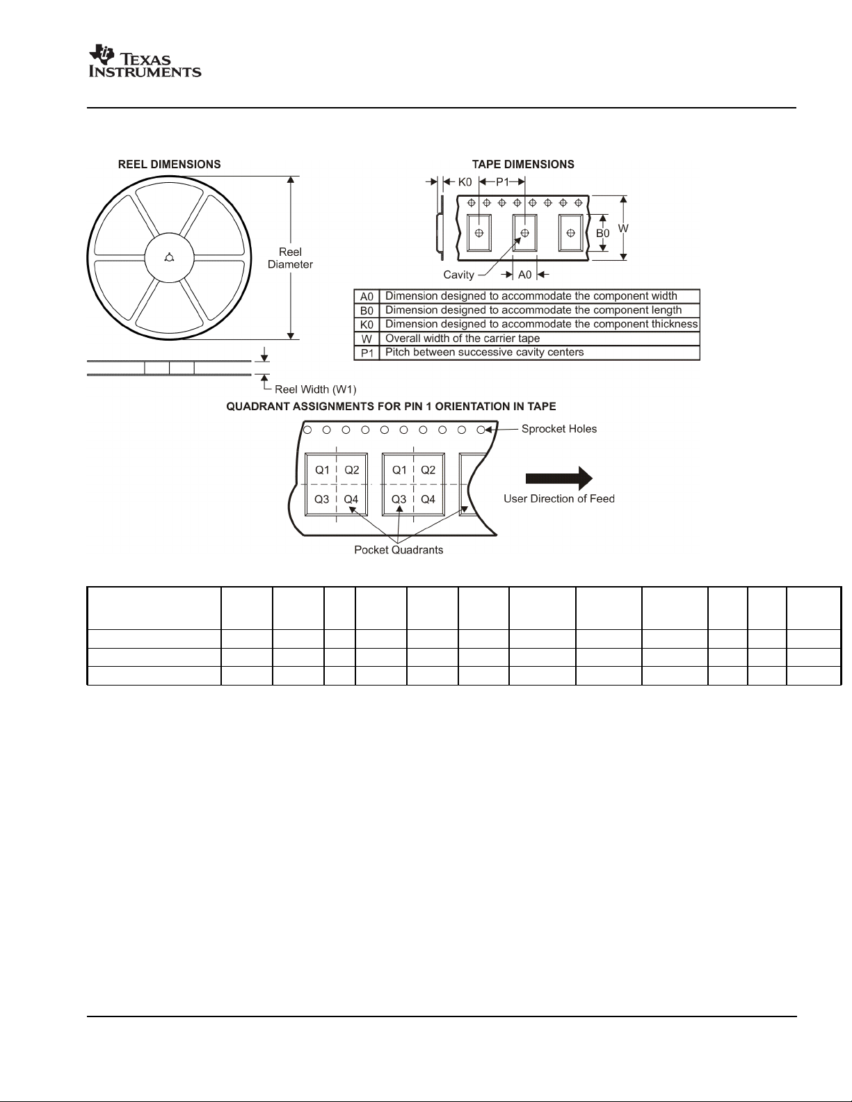
PACKAGE MATERIALS INFORMATION
www.ti.com
TAPE AND REEL INFORMATION
11-Mar-2008
*All dimensions are nominal
Device Package
Type
TPS40195PWR TSSOP PW 16 2000 330.0 12.4 7.0 5.6 1.6 8.0 12.0 Q1
TPS40195RGYR QFN RGY 16 3000 330.0 12.4 3.8 4.3 1.5 8.0 12.0 Q1
TPS40195RGYT QFN RGY 16 250 180.0 12.4 3.8 4.3 1.5 8.0 12.0 Q1
Package
Drawing
Pins SPQ Reel
Diameter
(mm)
Reel
Width
W1 (mm)
A0 (mm) B0 (mm) K0 (mm) P1
(mm)W(mm)
Pin1
Quadrant
Pack Materials-Page 1
Page 37

PACKAGE MATERIALS INFORMATION
www.ti.com
11-Mar-2008
*All dimensions are nominal
Device Package Type Package Drawing Pins SPQ Length (mm) Width (mm) Height (mm)
TPS40195PWR TSSOP PW 16 2000 346.0 346.0 29.0
TPS40195RGYR QFN RGY 16 3000 346.0 346.0 29.0
TPS40195RGYT QFN RGY 16 250 190.5 212.7 31.8
Pack Materials-Page 2
Page 38
MECHANICAL DAT A
MTSS001C – JANUARY 1995 – REVISED FEBRUARY 1999
PW (R-PDSO-G**) PLASTIC SMALL-OUTLINE PACKAGE
14 PINS SHOWN
0,65
1,20 MAX
14
0,30
0,19
8
4,50
4,30
PINS **
7
Seating Plane
0,15
0,05
8
1
A
DIM
14
0,10
6,60
6,20
M
0,10
0,15 NOM
2016
0°–8°
Gage Plane
24
0,25
0,75
0,50
28
A MAX
A MIN
NOTES: A. All linear dimensions are in millimeters.
B. This drawing is subject to change without notice.
C. Body dimensions do not include mold flash or protrusion not to exceed 0,15.
D. Falls within JEDEC MO-153
3,10
2,90
5,10
4,90
5,10
4,90
6,60
6,40
7,90
7,70
9,80
9,60
4040064/F 01/97
POST OFFICE BOX 655303 • DALLAS, TEXAS 75265
Page 39

Page 40

Page 41

Page 42

IMPORTANT NOTICE
Texas Instruments Incorporated and its subsidiaries (TI) reserve the right to make corrections, modifications, enhancements, improvements,
and other changes to its products and services at any time and to discontinue any product or service without notice. Customers should
obtain the latest relevant information before placing orders and should verify that such information is current and complete. All products are
sold subject to TI’s terms and conditions of sale supplied at the time of order acknowledgment.
TI warrants performance of its hardware products to the specifications applicable at the time of sale in accordance with TI’s standard
warranty. Testing and other quality control techniques are used to the extent TI deems necessary to support this warranty. Except where
mandated by government requirements, testing of all parameters of each product is not necessarily performed.
TI assumes no liability for applications assistance or customer product design. Customers are responsible for their products and
applications using TI components. To minimize the risks associated with customer products and applications, customers should provide
adequate design and operating safeguards.
TI does not warrant or represent that any license, either express or implied, is granted under any TI patent right, copyright, mask work right,
or other TI intellectual property right relating to any combination, machine, or process in which TI products or services are used. Information
published by TI regarding third-party products or services does not constitute a license from TI to use such products or services or a
warranty or endorsement thereof. Use of such information may require a license from a third party under the patents or other intellectual
property of the third party, or a license from TI under the patents or other intellectual property of TI.
Reproduction of TI information in TI data books or data sheets is permissible only if reproduction is without alteration and is accompanied
by all associated warranties, conditions, limitations, and notices. Reproduction of this information with alteration is an unfair and deceptive
business practice. TI is not responsible or liable for such altered documentation. Information of third parties may be subject to additional
restrictions.
Resale of TI products or services with statements different from or beyond the parameters stated by TI for that product or service voids all
express and any implied warranties for the associated TI product or service and is an unfair and deceptive business practice. TI is not
responsible or liable for any such statements.
TI products are not authorized for use in safety-critical applications (such as life support) where a failure of the TI product would reasonably
be expected to cause severe personal injury or death, unless officers of the parties have executed an agreement specifically governing
such use. Buyers represent that they have all necessary expertise in the safety and regulatory ramifications of their applications, and
acknowledge and agree that they are solely responsible for all legal, regulatory and safety-related requirements concerning their products
and any use of TI products in such safety-critical applications, notwithstanding any applications-related information or support that may be
provided by TI. Further, Buyers must fully indemnify TI and its representatives against any damages arising out of the use of TI products in
such safety-critical applications.
TI products are neither designed nor intended for use in military/aerospace applications or environments unless the TI products are
specifically designated by TI as military-grade or "enhanced plastic." Only products designated by TI as military-grade meet military
specifications. Buyers acknowledge and agree that any such use of TI products which TI has not designated as military-grade is solely at
the Buyer's risk, and that they are solely responsible for compliance with all legal and regulatory requirements in connection with such use.
TI products are neither designed nor intended for use in automotive applications or environments unless the specific TI products are
designated by TI as compliant with ISO/TS 16949 requirements. Buyers acknowledge and agree that, if they use any non-designated
products in automotive applications, TI will not be responsible for any failure to meet such requirements.
Following are URLs where you can obtain information on other Texas Instruments products and application solutions:
Products Applications
Amplifiers amplifier.ti.com Audio www.ti.com/audio
Data Converters dataconverter.ti.com Automotive www.ti.com/automotive
DSP dsp.ti.com Broadband www.ti.com/broadband
Clocks and Timers www.ti.com/clocks Digital Control www.ti.com/digitalcontrol
Interface interface.ti.com Medical www.ti.com/medical
Logic logic.ti.com Military www.ti.com/military
Power Mgmt power.ti.com Optical Networking www.ti.com/opticalnetwork
Microcontrollers microcontroller.ti.com Security www.ti.com/security
RFID www.ti-rfid.com Telephony www.ti.com/telephony
RF/IF and ZigBee® Solutions www.ti.com/lprf Video & Imaging www.ti.com/video
Mailing Address: Texas Instruments, Post Office Box 655303, Dallas, Texas 75265
Copyright © 2008, Texas Instruments Incorporated
Wireless www.ti.com/wireless
 Loading...