

1
2
3
4
10
9
8
7
HDRV
SW
BOOT
LDRV
ENABLE
FB
COMP
VDD
TPS40192/3
5 6BP5PGD
11
GND
UDG−06063
V
OUT
ON/OFF
External Logic
Supply
5V or Less,
or BP5
V
IN
V
OUT
TPS40192 , TPS40193
www.ti.com
SLUS719B – MARCH 2007 – REVISED SEPTEMBER 2007
4.5-V TO 18-V INPUT 10-PIN SYNCHRONOUS BUCK CONTROLLER WITH POWER GOOD
1
FEATURES CONTENTS
• Input Operating Voltage Range: 4.5 V to 18 V
• Up to 20-A Output Currents
• Supports Pre-Biased Outputs
• 0.5% 0.591-V Reference
• 600 kHz (TPS40192) and 300 kHz (TPS40193)
Switching Frequencies
• Three Selectable Thermally Compensated
Short Circuit Protection Levels
• Hiccup Restart from Faults
• Internal 5-V Regulator
• High and Low side FET RDS
Current
ON
Sensing
• 10-Pin 3 mm × 3 mm SON Package
• Internal 4-ms Soft-Start Time
• Thermal Shutdown Protection at 145 ° C
APPLICATIONS
• Cable Modem CPE
• Digital Set Top Box
• Graphics/Audio Cards
• Entry Level and Mid-Range Servers
Device Ratings 3
Electrical Characteristics 4
Typical Characteristics 6
Terminal Information 9
Application Information 11
Design Example 17
Additional References 27
DESCRIPTION
TPS40192 and TPS40193 are cost-optimized
synchronous buck controllers that operate from 4.5 V
to 18 V input. These controllers implement a
voltage-mode control architecture with the switching
frequency fixed at either 600 kHz (TPS40192) or 300
kHz (TPS40193). The higher switching frequency
facilitates the use of smaller inductor and output
capacitors, thereby providing a compact
power-supply solution. An adaptive anti-cross
conduction scheme is used to prevent shoot through
current in the power FETs.
1
Please be aware that an important notice concerning availability, standard warranty, and use in critical applications of
Texas Instruments semiconductor products and disclaimers thereto appears at the end of this data sheet.
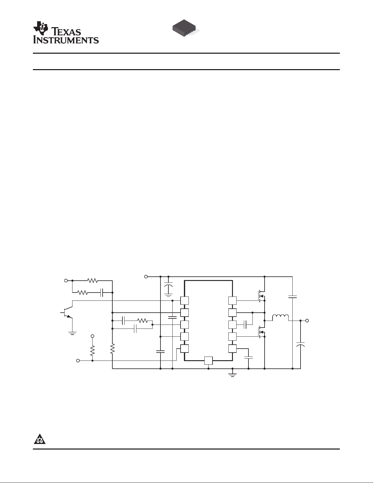
SIMPLIFIED APPLICATION DIAGRAM
PRODUCTION DATA information is current as of publication date.
Products conform to specifications per the terms of the Texas
Instruments standard warranty. Production processing does not
necessarily include testing of all parameters.
Copyright © 2007, Texas Instruments Incorporated
www.ti.com
TPS40192 , TPS40193
SLUS719B – MARCH 2007 – REVISED SEPTEMBER 2007
DESCRIPTION (continued)
Short circuit detection is done by sensing the voltage drop across the low-side MOSFET when it is on and
comparing it with a user selected threshold of 100 mV, 200 mV or 280 mV. The threshold is set with a single
external resistor connected from COMP to GND. This resistor is sensed at startup and the selected threshold is
latched. Pulse by pulse limiting (to prevent current runaway) is provided by sensing the voltage across the
high-side MOSFET when it is on and terminating the cycle when the voltage drop rises above a fixed threshold of
550 mV. When the controller senses an output short circuit, both MOSFETs are turned off and a timeout period
is observed before attempting to restart. This provides limited power dissipation in the event of a sustained fault.
ORDERING INFORMATION
T
J
-40 ° C to 85 ° C Plastic 10-Pin SON (DRC)
PACKAGE FREQUENCY (kHz) PART NUMBER
300
600
TAPE AND REEL
QUANTITY
250 TPS40193DRCT
3000 TPS40193DRCR
250 TPS40192DRCT
3000 TPS40192DRCR
2 Submit Documentation Feedback Copyright © 2007, Texas Instruments Incorporated
Product Folder Link(s): TPS40192 TPS40193
www.ti.com
TPS40192 , TPS40193
SLUS719B – MARCH 2007 – REVISED SEPTEMBER 2007
DEVICE RATINGS
ABSOLUTE MAXIMUM RATINGS
over operating free-air temperature range unless otherwise noted
VDD, ENABLE – 0.3 to 20
SW – 5 to 25
Input voltage range BOOT, HDRV – 0.3 to 30 V
BOOT-SW, HDRV-SW (differential from BOOT or HDRV to SW) -0.3 to 6
COMP, FB, BP5, LDRV, PGD – 0.3 to 6
T
Operating junction temperature range – 40 to 150
J
T
Storage temperature – 55 to 150
stg
(1) Stresses beyond those listed under "absolute maximum ratings" may cause permanent damage to the device. These are stress ratings
only, and functional operation of the device at these or any other conditions beyond those indicated under "recommended operating
conditions" is not implied. Exposure to absolute-maximum-rated conditions for extended periods may affect device reliability.
(1)
TPS40192/TPS40193 UNIT
RECOMMENDED OPERATING CONDITIONS
MIN NOM MAX UNIT
V
Input voltage 4.5 18 V
VDD
T
Operating Junction temperature -40 125 ° C
J
PACKAGE DISSIPATION RATINGS
R
High-K Board
PACKAGE AIRFLOW (LFM)
0 (Natural Convection) 47.9 2.08 0.835
DRC 200 40.5 2.46 0.987
400 38.2 2.61 1.04
(1) Ratings based on JEDEC High Thermal Conductivity (High K) Board. For more information on the test method, see TI Technical Brief
SZZA017.
θ JA
( ° C/W) TA= 25 ° C TA= 85 ° C
(1)
Power Rating (W) Power Rating (W)
° C
ELECTROSTATIC DISCHARGE (ESD) PROTECTION
MIN TYP MAX UNIT
Human Body Model (HBM) 2500
Charged Device Model (CDM) 1500
Copyright © 2007, Texas Instruments Incorporated Submit Documentation Feedback 3
Product Folder Link(s): TPS40192 TPS40193
V
www.ti.com
TPS40192 , TPS40193
SLUS719B – MARCH 2007 – REVISED SEPTEMBER 2007
ELECTRICAL CHARACTERISTICS
TJ= – 40 ° C to 85 ° C, V
REFERENCE
V
FB
INPUT SUPPLY
V
VDD
I
VDD
ON BOARD REGULATOR
V
5VBP
V
DO
I
SC
I
BP5
OSCILLATOR
f
SW
V
RMP
PWM
D
MAX
t
ON(min)
t
DEAD
SOFT-START
t
SS
t
SSDLY
t
REG
ERROR AMPLIFIER
GBWP Gain bandwidth product
A
OL
I
IB
I
EAOP
I
EAOM
SHORT CIRCUIT PROTECTION
t
PSS(min)
t
BLNK
t
OFF
V
ILIM
V
ILIMH
(1) Ensured by design. Not production tested.
Feedback voltage range mV
Input voltage range 4.5 18.0 V
Operating current
Output voltage V
Regulator dropout voltage V
Regulator current limit threshold 50
Average current 50
Switching frequency kHz
Ramp amplitude
Maximum duty cycle
Minimum controlled pulse
Output driver dead time
Soft-start time 3 4 6
Soft-start delay time 2 ms
Time to regulation 6
DC gain
Input bias current (current out of FB
pin)
Output source current V
Output sink current V
Minimum pulse during short circuit
Blanking time
Off-time between restart attempts 30 50 ms
Short circuit comparator threshold
voltage
Short circuit threshold voltage on
high-side MOSFET
= 12 Vdc, all parameters at zero power dissipation (unless otherwise noted)
VDD
PARAMETER TEST CONDITIONS MIN TYP MAX UNIT
(1)
(1)
(1)
(1)
(1)
0 ° C ≤ TJ≤ 85 ° C 588 591 594
-40 ° C ≤ TJ≤ 85 ° C 585 591 594
V
V
= 3 V 2.5 4.0 mA
ENABLE
= 0.6 V 45 70 μ A
ENABLE
> 6 V, I
VDD
- V
VDD
BP5
≤ 10 mA 5.1 5.3 5.5 V
5VBP
, V
= 5 V, I
VDD
≤ 25 mA 350 550 mV
BP5
TPS40193 240 300 360
TPS40192 500 600 700
85%
(1)
HDRV off to LDRV on 50 ns
LDRV off to HDRV on 25
7 10 MHz
60 dB
= 0 V 1
FB
= 2 V 1
FB
(1)
60 90 120
R
COMP(GND)
R
COMP(GND)
R
COMP(GND)
= OPEN, TJ= 25 ° C 160 200 240
= 4 k Ω , TJ= 25 ° C 80 100 120
= 12 k Ω , TJ= 25 ° C 228 280 342
TJ= 25 ° C 400 550 650
1 V
250
mA
110
100 nA
mA
ns
mV
4 Submit Documentation Feedback Copyright © 2007, Texas Instruments Incorporated
Product Folder Link(s): TPS40192 TPS40193
www.ti.com
ELECTRICAL CHARACTERISTICS (continued)
TJ= – 40 ° C to 85 ° C, V
OUTPUT DRIVERS
R
HDHI
R
HDLO
R
LDHI
R
LDLO
t
HRISE
t
HFALL
t
LRISE
t
LFALL
UVLO
V
UVLO
UVLO
SHUTDOWN
V
IH
V
IL
POWER GOOD
V
OV
V
UV
V
PG_HYST
R
PGD
I
PDGLK
BOOT DIODE
V
DFWD
THERMAL SHUTDOWN
T
JSD
T
JSDH
(2) Ensured by design. Not production tested.
High-side driver pull-up resistance V
High-side driver pull-down resistance V
Low-side driver pull-up resistance I
Low-side driver pull-down resistance I
High-side driver rise time
High-side driver fall time
Low-side driver rise time
Low-side driver fall time
Turn-on voltage 3.9 4.2 4.4 V
Hysteresis 700 800 900 mV
HYST
High-level input voltage, ENABLE 1.9 3.0
Low-level input votlage, ENABLE 0.6
Feedback voltage limit for powergood 650
Feedback voltage limit for powergood 525 mV
Powergood hysteresis voltage at FB pin 30
Pulldown resistance of PGD pin V
Leakage current V
Bootstrap diode forward voltage I
Junction shutdown temperature
Hysteresis
= 12 Vdc, all parameters at zero power dissipation (unless otherwise noted)
VDD
PARAMETER TEST CONDITIONS MIN TYP MAX UNIT
(2)
TPS40192 , TPS40193
SLUS719B – MARCH 2007 – REVISED SEPTEMBER 2007
- V
BOOT
BOOT
LDRV
(2)
(2)
(2)
(2)
(2)
LDRV
C
LOAD
= 0 V 7 50 Ω
FB
= 0 V 7 12 μ A
FB
BOOT
= 4.5 V, I
SW
- V
= 4.5 V, I
SW
= -100 mA 2.5 5.0
= 100 mA 0.8 1.5
= 1 nF ns
= 5 mA 0.5 0.8 1.2 V
= -100 mA 3 6
HDRV
= 100 mA 1.5 3.0
HDRV
15 35
10 25
15 35
10 25
145
20
Ω
V
° C
Copyright © 2007, Texas Instruments Incorporated Submit Documentation Feedback 5
Product Folder Link(s): TPS40192 TPS40193
www.ti.com
TJ − Junction Temperature − °C
V
FB
− Relative Reverefnce Voltage Change − %
−40 −25 −10 5 20 35 95 12550 65 80 110
−0.50
−0.45
−0.40
−0.20
−0.15
−0.05
−0.35
−0.30
−0.25
0.00
0.50
−0.10
−40 −25 −10 5 20 35 95 125
−4.5
−4.0
−3.5
−1.5
−1.0
−0.5
0.5
−3.0
−2.5
−2.0
0.0
50 65 80 110
f
SW
− Relative Oscillator Frequency Change − %
TJ − Junction Temperature − °C
I
VDD
− Shutdown Current − µA
TJ − Junction Temperature − °C
0
10
20
30
40
50
60
−40 −25 −10 5 20 35 9550 65 80 110 125
V
ENABLE
< 0.6 V
V
ENABLE
− Enable Threshold Voltage − V
TJ − Junction Temperature − °C
0
0.5
1.0
1.5
2.0
2.5
−40 −25 −10 5 20 35 95 12550 65 80 110
Turn On
Turn Off
TPS40192 , TPS40193
SLUS719B – MARCH 2007 – REVISED SEPTEMBER 2007
TYPICAL CHARACTERISTICS
RELATIVE REFERENCE FEEDBACK VOLTAGE RELATIVE OSCILLATOR FREQUENCY CHANGE
vs vs
JUNCTION TEMPERATURE JUNCTION TEMPERATURE
Figure 1. Figure 2.
SHUTDOWN INPUT CURRENT ENABLE THRESHOLD VOLTAGE
vs vs
JUNCTION TEMPERATURE JUNCTION TEMPERATURE
Figure 3. Figure 4.
6 Submit Documentation Feedback Copyright © 2007, Texas Instruments Incorporated
Product Folder Link(s): TPS40192 TPS40193
www.ti.com
t
SS
− Soft start Time − ms
TJ − Junction Temperature − °C
3.75
3.80
3.85
3.90
3.95
4.00
4.05
−40 −25 −10 5 20 35 95 12550 65 80 110
−40 −25 −10 5 20 35 95 12550 65 80 110
0
50
150
200
250
350
400
100
300
V
ILIM
− Current Limit Threshold − mV
TJ − Junction Temperature − °C
R
COMP
= 4 kΩ
R
COMP
= OPEN
R
COMP
= 12 kΩ
0
100
300
400
600
700
800
500
200
−40 −25 −10 5 20 35 95 12550 65 80 110
V
ILIMH
− Current Limit Threshold − mV
TJ − Junction Temperature − °C
t
REG
− Regulation Time − ms
TJ − Junction Temperature − °C
4.4
5.3
5.7
6.1
6.3
5.5
4.7
−40 −25 −10 5 20 35 95 12550 65 80 110
4.9
5.1
5.5
5.9
TYPICAL CHARACTERISTICS (continued)
TPS40192 , TPS40193
SLUS719B – MARCH 2007 – REVISED SEPTEMBER 2007
SOFT START TIME LOW-SIDE MOSFET CURRENT LIMIT THRESHOLD
vs vs
JUNCTION TEMPERATURE JUNCTION TEMPERATURE
Figure 5. Figure 6.
HIGH-SIDE MOSFET CURRENT LIMIT THRESHOLD TOTAL TIME TO REGULATION
vs vs
JUNCTION TEMPERATURE JUNCTION TEMPERATURE
Copyright © 2007, Texas Instruments Incorporated Submit Documentation Feedback 7
Figure 7. Figure 8.
Product Folder Link(s): TPS40192 TPS40193
www.ti.com
4 6 8 10 12 14 16 18
0
10
40
70
80
100
60
30
20
90
50
I
VDD
− Supply Current − µA
V
VDD
− Input Voltage − V
V
ENABLE
< 0.6 V
V
OV
, V
UV
− Powergood Threshold Voltage − mV
TJ − Junction Temperature − °C
560
580
540
520
500
660
680
640
620
600
−40 −25 −10 5 20 35 95 12550 65 80 110
Overvoltage
Undervoltage
0.4 0.6 0.8 1.0 1.2 1.4 1.6
0
0.5
3.0
3.5
4.5
1.5
1.0
5.0
2.0
2.5
4.0
1-D - Freewheel Time - ms
I
OC
- Relative Overcurrent Trip Point - A
TPS40192 , TPS40193
SLUS719B – MARCH 2007 – REVISED SEPTEMBER 2007
TYPICAL CHARACTERISTICS (continued)
POWERGOOD THRESHOLD VOLTAGE SHUTDOWN CURRENT
vs vs
JUNCTION TEMPERATURE INPUT VOLTAGE
Figure 9. Figure 10.
RELATIVE OVERCURRENT TRIP POINT
vs
FREEWHEEL TIME
8 Submit Documentation Feedback Copyright © 2007, Texas Instruments Incorporated
Figure 11.
Product Folder Link(s): TPS40192 TPS40193
www.ti.com
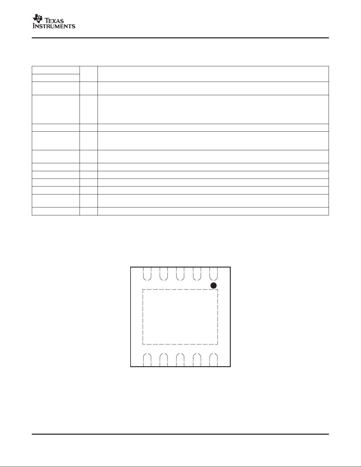
DRC PACKAGE
(TOP VIEW)
PGD5VDD4COMP3FB2ENABLE
1
6 7 8 9 10
BP5 LDRV BOOT SW HDRV
TPS40192
TPS40193
TPS40192 , TPS40193
SLUS719B – MARCH 2007 – REVISED SEPTEMBER 2007
DEVICE INFORMATION
Table 1. TERMINAL FUNCTIONS
TERMINAL
NAME NO.
BOOT 8 I
BP5 6 O 25nC or greater. Low power, low noise loads may be connected here if desired. The sum of the external
COMP 3 O Output of the error amplifier.
ENABLE 1 I controller on. A weak internal pull-up holds this pin high so that the pin may be left floating if this function is
FB 2 I
GND (11) - Thermal pad ground connection. Common reference for the device. Connect to the system GND.
HDRV 10 O Bootstrapped output for driving the gate of the high side N channel FET.
LDRV 7 O Output to the rectifier MOSFET gate
PGD 5 O Open drain power good output
SW 9 I
VDD 4 I Power input to the controller
I/O DESCRIPTION
Gate drive voltage for the high-side N-channel MOSFET. A capacitor 100 nF typical must be connected
between this pin and SW.
Output bypass for the internal regulator. Connect at least 1 μ F capacitor from this pin to GND. Larger
capacitors, up to 4.7 μ F will improve noise performance when using a low side FET with a gate charge of
load and the gate drive requirements must not exceed 50 mA. This regulator is turned off when ENABLE is
pulled low.
Logic level input which starts or stops the controller from an external user command. A high-level turns the
not used.
Inverting input to the error amplifier. In normal operation the voltage on this pin is equal to the internal
reference voltage (591 mV typical)
Sense line for the adaptive anti-cross conduction circuitry. Serves as common connection for the flying high
side MOSFET driver
Copyright © 2007, Texas Instruments Incorporated Submit Documentation Feedback 9
Product Folder Link(s): TPS40192 TPS40193
www.ti.com
ENABLE 1
VDD
4
BP5
6
COMP 3
FB
2
GND
PP
5 V
Regulator
4.2 V
+
5 V
UVLO
+
Error
Amplifier
591 mV
SS
+
Fault
Controller
Soft Start
Ramp
Generator
PWM Logic
and
Anti-Cross
Conduction
+
VDD - 0.5 V
Oscillator
Short Circuit
Threshold
Selector
SD
UVLO
UVLO
SS
SD
FAULT
UVLO
+
CLK
10CLK
8
7
9
5
ENABLE
HDRV
SW
LDRV
PGD
5 V
Powergood
Control
FB
SD
FAULT
5 V
SC Threshold Latch
SC: -110 mV, -200 mV, or -280 mV
750 kW
VDD
SC
SD
+
FAULT
OCL
OCH
UDG-06064
TPS40192 , TPS40193
SLUS719B – MARCH 2007 – REVISED SEPTEMBER 2007
10 Submit Documentation Feedback Copyright © 2007, Texas Instruments Incorporated
Product Folder Link(s): TPS40192 TPS40193

www.ti.com
TPS40192 , TPS40193
SLUS719B – MARCH 2007 – REVISED SEPTEMBER 2007
APPLICATION INFORMATION
Introduction
The TPS40192 and TPS40193 are cost optimized controllers providing all the necessary features to construct a
high performance DC/DC converter while keeping costs to a minimum. Support for pre-biased outputs eliminates
concerns about damaging sensitive loads during startup. Strong gate drivers for the high side and rectifier
N-channel MOSFETs decrease switching losses for increased efficiency. Adaptive gate drive timing prevents
shoot through and minimizes body diode conduction in the rectifier MOSFET, also increasing efficiency.
Selectable short circuit protection thresholds and hiccup recovery from a short circuit increase design flexibility
and minimize power dissipation in the event of a prolonged output fault. A dedicated enable pin (ENABLE) allows
the converter to be placed in a very low quiescent current shutdown mode. Internally fixed switching frequency
and soft-start time reduce external component count, simplifying design and layout, as well as reducing footprint
and cost. The 3 mm × 3 mm package size also contributes to a reduced overall converter footprint.
Voltage Reference
The band gap cell is designed with a trimmed 591 mV output. The 0.5% tolerance on the reference voltage
allows the user to design a very accurate power-supply.
Oscillator
The TPS40192 has a fixed internal switching frequency of 600 kHz while the TPS40193 operates at 300 kHz.
UVLO
When the input voltage is below the UVLO threshold, the device holds all gate drive outputs in the low (OFF)
state. When the input rises above the UVLO threshold, and the ENABLE pin is above the turn ON threshold, the
oscillator begins to operate and the start-up sequence is allowed to begin. The UVLO level is internally fixed at
4.2 V.
Copyright © 2007, Texas Instruments Incorporated Submit Documentation Feedback 11
Product Folder Link(s): TPS40192 TPS40193
www.ti.com
4
1
5
To
Enable
Chip
VDD
ENABLE
GND
1.5 MΩ
200 kΩ
1 kΩ
1 kΩ
300 kΩ
200 Ω
UDG−05061
TPS40192 , TPS40193
SLUS719B – MARCH 2007 – REVISED SEPTEMBER 2007
Enable Functionality
The TPS40192 and TPS40193 have a dedicated ENABLE pin. This simplifies user level interface design since
no multiplexed functions exist. Another benefit is a true low power shutdown mode of operation. When the
ENABLE pin is pulled to GND, all unnecessary functions, including the BP5 regulator, are turned off, reducing the
device IDD current to 45-uA. A functionally equivalent circuit of the enable circuitry shown in Figure 12 .
Figure 12. TPS40192 ENABLE Pin Internal Circuitry
If the ENABLE pin is left floating, the chip starts automatically. The pin must be pulled to less than 600 mV to
guarantee that the TPS40192/3 is in shutdown mode. Note that the ENABLE pin is relatively high impedance. In
some situations, there could be enough noise nearby to cause the ENABLE pin to swing below the 600 mV
threshold and give erroneous shutdown commands to the rest of the device. There are two solutions to this
problem should it arise.
1. Place a capacitor from ENABLE to GND. A side effect of this is to delay the start of the converter while the
capacitor charges past the enable threshold
2. Place a resistor from VDD to ENABLE. This causes more current to flow in the shutdown mode, but does not
delay converter startup. If a resistor is used, the total current into the ENABLE pin should be limited to no
more than 500 μ A.
12 Submit Documentation Feedback Copyright © 2007, Texas Instruments Incorporated
Product Folder Link(s): TPS40192 TPS40193

www.ti.com
ENABLE
COMP
VOUT
SC Threshold
Configured
(1 ms)
Soft Start Time (4 ms)
Compensation
Network Zeroed
(1 ms)
UDG−06062
TPS40192 , TPS40193
SLUS719B – MARCH 2007 – REVISED SEPTEMBER 2007
Startup Sequence and Timing
The TPS40192/3 startup sequence is as follows. After input power is applied, the 5-V onboard regulator comes
up. Once this regulator comes up, the device goes through a period where it samples the impedance at the
COMP pin and determines the short circuit protection threshold voltage, by placing 400 mV on the COMP pin for
approximately 1 ms. During this time, the current is measured and compared against internal thresholds to select
the short circuit protection threshold. After this, the COMP pin is brought low for 1 ms. This ensures that the
feedback loop is preconditioned at startup and no sudden output rise occurs at the output of the converter when
the converter is allowed to start switching. After these initial two milliseconds, the internal soft-start circuitry is
engaged and the converter is allowed to start. See Figure 13 .
Figure 13. Startup Sequence
Copyright © 2007, Texas Instruments Incorporated Submit Documentation Feedback 13
Product Folder Link(s): TPS40192 TPS40193

www.ti.com
0.4 V
R1
e
ǒ
*t
R1 C1
Ǔ
t 10 mA
2
C1
R1
C2
3
COMP
TPS40192/3
FB
UDG−06061
V
OUT
R
COMP
TPS40192 , TPS40193
SLUS719B – MARCH 2007 – REVISED SEPTEMBER 2007
Selecting the Short Circuit Current
A short circuit in the TPS40192/3 is detected by sensing the voltage drop across the low-side FET when it is on,
and across the high-side FET when it is on. If the voltage drop across either FET exceeds the short circuit
threshold in any given switching cycle, a counter increments one count. If the voltage across the high-side FET
was higher that the short circuit threshold, that FET is turned off early. If the voltage drop across either FET does
not exceed the short circuit threshold during a cycle, the counter is decremented for that cycle. If the counter fills
up (a count of 7) a fault condition is declared and the drivers turn off both MOSFETs. After a timeout of
approximately 50 ms, the controller attempts to restart. If a short circuit is still present at the output, the current
quickly ramps up to the short circuit threshold and another fault condition is declared and the process of waiting
for the 50 ms an attempting to restart repeats. The low side threshold will increase as the low side on time
decreases due to blanking time and comparator response time. See Figure 11 for changes in the threshold as
the low side FET conduction time decreases.
The TPS40192/3 provides three selectable short circuit protection thresholds for the low side FET: 100 mV,
200 mV and 280 mV. The particular threshold is selected by connecting a resistor from COMP to GND. Table 2
shows the short circuit thresholds for corresponding resistors from COMP to GND. When designing the
compensation for the feedback loop, remember that a low impedance compensation network combined with a
long network time constant can cause the short circuit threshold setting to not be as expected. The time constant
and impedance of the network connected from COMP to FB should be as in Equation 1 to guarantee no
interaction with the short circuit threshold setting.
where
• t is 1 ms, the sampling time of the short circuit threshold setting circuit
• R1 and C1 are the values of the components in Figure 14
(1)
Figure 14. Short Circuit Threshold Feedback Network
14 Submit Documentation Feedback Copyright © 2007, Texas Instruments Incorporated
Product Folder Link(s): TPS40192 TPS40193

www.ti.com
I
SCP(max)
+
V
ILIM(max)
R
DS(on)min
I
SCP(min)
+
V
ILIM(min)
R
DS(on)max
I
OUT(max)
+
V
ILIM(min)
R
DS(on)max
TPS40192 , TPS40193
SLUS719B – MARCH 2007 – REVISED SEPTEMBER 2007
Table 2. Short Circuit Threshold Voltage Selection
COMPARATOR RESISTANCE CURRENT LIMIT THRESHOLD
The range of short circuit current thresholds that can be expected is shown in Equation 2 and Equation 3 .
where
• I
• V
• R
is the short circuit current
SCP
is the short circuit threshold for the low-side MOSFET
ILIM
is the channel resistance of the low-side MOSFET
DS(on)
Note that due to blanking time considerations, overcurrent threshold accuracy may fall off for duty cycle greater
than 75% with the TPS40192, or 88% with the TPS40193. The reason for this is that the over current comparator
will have only a very short time to sample the SW pin voltage under these conditions and may not have time to
respond to voltages very near the threshold.
The short circuit protection threshold for the high-side MOSFET is fixed at 550 mV typical, 400 mV minimum.
This threshold is in place to provide a maximum current output using pulse by pulse current limit in the case of a
fault. The pulse will be terminated when the voltage drop acros the high side FET exceeds the short circuit
threshold. The maximum amount of current that can be guaranteed to be sourced from a converter can be found
by Equation 4 .
R
(k Ω ) VOLTAGE (mV)
COMP
12 ± 10% 280
Open 200
4 ± 10% 100
V
(V)
ILIM
(2)
(3)
where
• I
OUT(max)
• V
• R
If the required current from the converter is greater than the calculated I
is the maximum current that the converter is guaranteed to source
ILIMH(min)
DS(on)max
is the short circuit threshold for the high-side MOSFET (400 mV)
is the maximum resistance of the high-side MOSFET
OUT(max)
, a lower resistance high-side
MOSFET must be chosen. Both the high side and low side thresholds use temperature compensation to
approximate the change in resistance for a typical power MOSFET. This will help couneract shifts in overcurrent
thresholds as temperature increases. For this to be effective, the MOSFETs and the IC must be well coupled
thermally.
(4)
Copyright © 2007, Texas Instruments Incorporated Submit Documentation Feedback 15
Product Folder Link(s): TPS40192 TPS40193

www.ti.com
IG+ f
SW
ǒ
Q
G (high)
) Q
G (low)
Ǔ
TPS40192 , TPS40193
SLUS719B – MARCH 2007 – REVISED SEPTEMBER 2007
5-V Regulator
These devices have an on board 5-V regulator that allows the parts to operate from a single voltage feed. No
separate 5-V feed to the part is required. This regulator needs to have a minimum of 1- μ F of capacitance on the
BP5 pin to guarantee stability. A ceramic capacitor is suggested for this purpose.
This regulator can also be used to supply power to nearby circuitry, eliminating the need for a separate LDO in
some cases. If this pin is used for external loads, be aware that this is the power supply for the internals of the
TPS40192/3. While efforts have been made to reduce sensitivity, any noise induced on this line has an adverse
effect on the overall performance of the internal circuitry and shows up as increased pulse jitter, or skewed
reference voltage. Also, when the device is disabled by pulling the EN pin low, this regulator is turned off and will
not be available to supply power.
The amount of power available from this pin varies with the size of the power MOSFETs that the drivers must
operate. Larger MOSFETs require more gate drive current and reduce the amount of power available on this pin
for other tasks. The total current that can be drwan from this pin by both the gate drive and external loads cannot
exceed 50mA. The IC itself will use up to 4mA from the regulator and the total gate drive current can be found
from Equation 5 .
For regulator stability, a 1- μ F capacitor is required to be connected from BP5 to GND. In some applications using
higher gate charge MOSFETs, a larger capacitor is required for noise suppression. For a total gate charge of
both the high and low side MOSFETs greater than 20 nC, a 2.2- μ F or larger capacitor is recommended.
where
• IGis the required gate drive current
• fSWis the switching frequency (600 kHz for TPS40192, and 300 kHz for TPS40193)
• Q
• Q
is the gate charge requirement for the high-side FET when V
G(high)
is the gate charge requirement for the low-side FET when V
G(low)
=5 V
GS
=5 V
GS
(5)
16 Submit Documentation Feedback Copyright © 2007, Texas Instruments Incorporated
Product Folder Link(s): TPS40192 TPS40193

www.ti.com
TPS40192 , TPS40193
SLUS719B – MARCH 2007 – REVISED SEPTEMBER 2007
Pre-Bias Startup
The TPS40192/3 contains a unique circuit to prevent current from being pulled from the output during startup in
the condition the output is pre-biased. When the soft-start commands a voltage higher than the pre-bias level
(internal soft-start becomes greater than feedback voltage [V
rectification by starting the first LDRV pulses with a narrow on-time. It then increments that on-time on a
cycle-by-cycle basis until it coincides with the time dictated by (1-D), where D is the duty cycle of the converter.
This scheme prevents the initial sinking of the pre-bias output, and ensures that the out voltage (V
ramps up smoothly into regulation and the control loop is given time to transition from pre-biased startup to
normal mode operation with minimal disturbance to the output voltage. The amount of time from the start of
switching until the low-side MOSFET is turned on for the full (1-D) interval is defined by 32 clock cycles.
Drivers
The drivers for the external HDRV and LDRV MOSFETs are capable of driving a gate-to-source voltage of 5 V.
The LDRV driver switches between VDD and GND, while HDRV driver is referenced to SW and switches
between BOOT and SW. The drivers have non-overlapping timing that is governed by an adaptive delay circuit to
minimize body diode conduction in the synchronous rectifier. The drivers are capable of driving MOSFETS that
are appropriate for a 15-A (TPS40192) or 20A (TPS40193) converter.
Power Good
The TPS40192/3 provides an indication that output power is good for the converter. This is an open drain signal
and pulls low when any condition exists that would indicate that the output of the supply might be out of
regulation. These conditions include:
• V
• soft-start is active
• an undervoltage condition exists for the device
• a short circuit condition has been detected
• die temperature is over (145 ° C)
is more than ± 10% from nominal
FB
]), the controller slowly activates synchronous
FB
) starts and
OUT
NOTE:
When there is no power to the device, PGOOD is not able to pull close to GND if an
auxiliary supply is used for the power good indication. In this case, a built in resistor
connected from drain to gate on the PGOOD pull down device makes the PGOOD pin
look approximately like a diode to GND.
Thermal Shutdown
If the junction temperature of the device reaches the thermal shutdown limit of 145 ° C, the PWM and the oscillator
are turned off and HDRV and LDRV are driven low, turning off both FETs. When the junction cools to the
required level (125 ° C nominal), the PWM inititates soft start as during a normal power up cycle.
Copyright © 2007, Texas Instruments Incorporated Submit Documentation Feedback 17
Product Folder Link(s): TPS40192 TPS40193

www.ti.com
TPS40192 , TPS40193
SLUS719B – MARCH 2007 – REVISED SEPTEMBER 2007
Layout Recommendations and Sample Layout
Layout Recommendations:
• PowerPad™ is the device ’ s(U1) only GND connection. PowerPad™ must be connected to ground.
• PowerPad™ should be directly connected to SYNC FET (Q3) source with short, wide trace.
• Locate 3-5 vias in PowerPad™ land to remove heat from the device.
• Connect input capacitors (C7 & C9) and output capacitors (C8 & C10) grounds directly to SYNC FET (Q3)
source with wide copper trace or solid power ground island.
• Locate input capacitors (C7 & C9), MOSFETs (Q2 & Q3), inductor (L1) and output capacitor (C8 & C10) over
power ground island.
• Use short, wide traces for LDRV and HDRV MOSFET connections.
• Route SW trace near HDRV trace.
• Route GND trace near LDRV trace.
• Use separate analog ground island under feedback components (C1, C2, C3, R5, R6, R7, R8 & R10).
• Connect ground islands at PowerPad™ with 10-mil wide trace opposite SYNC FET (Q2) source connection.
Sample Layout:
Figure 15. TPS40192/3 Sample Layout - Component Placement and Top Side Copper
Figure 16. TPS40192/3 Sample Layout - Bottom Side Copper (X-Ray view from Top)
18 Submit Documentation Feedback Copyright © 2007, Texas Instruments Incorporated
Product Folder Link(s): TPS40192 TPS40193

www.ti.com
TPS40192 , TPS40193
SLUS719B – MARCH 2007 – REVISED SEPTEMBER 2007
DESIGN EXAMPLE
Introduction
This example illustrates the design process and component selection for a 12 V to 1.8 V point-of-load
synchronous buck regulator using the TPS40192. A definition of symbols used can be found in Table 8 of this
datasheet.
Table 3. Design Example Electrical Characteristics
PARAMETER TEST CONDITION MIN NOM MAX UNIT
V
V
)
V
V
V
V
I
OUT
I
SCP
η Efficiency VIN=12 V, I
f
SW
Input voltage 8 14
IN
IN(ripple
Input ripple I
Output voltage 0 A ≤ I
OUT
= 10 A 0.6 V
OUT
≤ 10 A 1.764 1.800 1.836
OUT
Line regulation 8.0 V ≤ VIN≤ 14 V 0.5%
Load regulation 0 A ≤ I
Output ripple I
RIPPLE
Output overshoot 3 A ≤ I
OVER
Output undershoot 50
UNDER
OUT
≤ 10 A 0.5%
OUT
= 10 A 36
≤ 7 A 50 mV
OUT
Output current 0 10
Short circuit current trip point
= 5 A 90%
OUT
Switching frequency 600 kHz
Size
A
The list of materials for this application is shown Table 7 . The efficiency, line and load regulation from boards
built using this design are shown in Figure 17 and Table 3 . Gerber Files and additional application information
are available from the factory.
Figure 17. TPS40192 Sample Schematic
Copyright © 2007, Texas Instruments Incorporated Submit Documentation Feedback 19
Product Folder Link(s): TPS40192 TPS40193

www.ti.com
L [
V
IN(max)
* V
OUT
0.3 I
OUT
V
OUT
V
IN(max)
1
f
SW
I
L(rms)
+
ǒ
I
L(avg)
Ǔ
2
)
1
12
ǒ
I
RIPPLE
Ǔ
2
Ǹ
+
ǒ
I
OUT
Ǔ
2
)
1
12
ǒ
I
RIPPLE
Ǔ
2
Ǹ
TPS40192 , TPS40193
SLUS719B – MARCH 2007 – REVISED SEPTEMBER 2007
Design Procedure
Selecting the Switching Frequency
For this design the TPS40192, with fSW= 600 kHz, is selected to reduce inductor and capacitor sizes.
Inductor Selection
The inductor is typically sized for approximately 30% peak-to-peak ripple current (I
current, the required inductor size can be calculated by Equation 6 .
Solving this for
• V
• V
• I
• fSW= 600 kHz
an inductor value of 0.87 μ H is obtained.
A standard value of 1.0 μ H is selected. Solving for I
The RMS current through the inductor is approximated by Equation 7 .
= 14 V
IN(max)
= 1.8 V
OUT
= 10A
OUT
with 1.0 μ H results in 2.6-A peak-to-peak ripple.
RIPPLE
RIPPLE
). Given this target ripple
(6)
Using Equation 7 , the maximum RMS current in the inductor is approximately 10.03 A
(7)
20 Submit Documentation Feedback Copyright © 2007, Texas Instruments Incorporated
Product Folder Link(s): TPS40192 TPS40193

www.ti.com
V
OVER
t
I
TRAN
C
OUT
DT +
I
TRAN
C
OUT
I
TRAN
L
V
OUT
+
ǒ
I
TRAN
Ǔ
2
L
V
OUT
C
OUT
V
UNDER
t
I
TRAN
C
OUT
DT +
I
TRAN
C
OUT
I
TRAN
L
VIN* V
OUT
+
ǒ
I
TRAN
Ǔ
2
L
ǒ
VIN* V
OUT
Ǔ
C
OUT
C
OUT(min)
+
ǒ
I
TRAN(max)
Ǔ
2
L
V
OUT
V
OVER
ESR
MAX
t
V
RIPPLE(tot)
* V
RIPPLE(cap)
C
OUT
+
V
RIPPLE(tot)
*
ǒ
I
RIPPLE
C
OUT fSW
Ǔ
I
RIPPLE
I
CHARGE
+
V
OUT
C
OUT
T
SS
I
L(peak)
+ I
OUT(max)
)
1
2
I
RIPPLE
) I
CHARGE
TPS40192 , TPS40193
SLUS719B – MARCH 2007 – REVISED SEPTEMBER 2007
Output Capacitor Selection (C8)
The selection of the output capacitor is typically driven by the output transient response. The Equation 8 and
Equation 9 overestimate the voltage deviation to account for delays in the loop bandwidth and can be used to
determine the required output capacitance.
If
• V
• V
Based on a 4-A load transient with a maximum 50 mV overshoot at 8.0 V input, calculate a minimum 178- μ F
output capacitance.
With a minimum capacitance, the maximum allowable ESR is determined by the maximum ripple voltage and is
approximated by Equation 11 .
> 2 × V
IN(min)
< 2 × V
IN(min)
, use overshoot to calculate minimum output capacitance.
OUT
, use undershoot to calculate minimum output capacitance.
OUT
(8)
(9)
(10)
Based on 178 μ F of capacitance, 2.6-A ripple current, 600-kHz switching frequency and 36-mV ripple voltage,
calculate a capacitive ripple of 24.3 mV and a maximum ESR of 4.4 m Ω .
Two 1206 100- μ F, 6.3-V X5R ceramic capacitors are selected to provide more than 178- μ F of minimum
capacitance and less than 4.4 m Ω of ESR (2.5 m Ω each).
Peak Current Rating of the Inductor
With output capacitance, it is possible to calculate the charge current during start-up and determine the minimum
saturation current rating for the inductor. The start-up charging current is approximated by Equation 12 .
Using the TPS40192's minimum soft-start time of 3.0 ms, C
= 240 μ F and V
OUT
OUT
= 1.8 V, I
CHARGE
= 144 mA.
Table 4. Inductor Requirements
PARAMETER SYMBOL VALUE UNITS
Inductance L 1.0 μ H
RMS current (thermal rating) I
Peak current (saturation rating) I
L(rms)
L(peak)
10.03
11.3
A
A PG0083.102 1.0- μ H is selected for its small size, low DCR (6.6 m Ω ) and high current handling capability (12 A
thermal, 17 A saturation)
(11)
(12)
(13)
Copyright © 2007, Texas Instruments Incorporated Submit Documentation Feedback 21
Product Folder Link(s): TPS40192 TPS40193

www.ti.com
C
IN(min)
+
I
LOAD
V
OUT
V
RIPPLE(cap)
VIN f
SW
ESR
MAX
+
V
RIPPLE(esr)
I
LOAD
)
1
2
I
RIPPLE
I
RMS(Cin)
+ I
IN(rms)
* I
IN(avg)
+
ǒ
I
OUT
)
1
12
I
RIPPLE
Ǔ
V
OUT
V
IN
Ǹ
*
V
OUT
I
OUT
V
IN
TPS40192 , TPS40193
SLUS719B – MARCH 2007 – REVISED SEPTEMBER 2007
Input Capacitor Selection (C7)
The input voltage ripple is divided between capacitance and ESR. For this design V
V
RIPPLE(ESR)
For this design C
= 200 mV. The minimum capacitance and maximum ESR are estimated by Equation 14 .
> 9.375 μ F and ESR < 17.7 m Ω . The RMS current in the input capacitors is estimated by
IN
RIPPLE(cap)
Equation 16 .
For this design V
= 14 V, V
IN
OUT
= 1.8 V, I
=10 A and I
OUT
= 2.6 A calculate an RMS of 2.37 A, so the total
RIPPLE
of our input capacitors must support 2.37 A of RMS ripple current.
Two 1210 10- μ F 25V X5R ceramic capacitors with about 2 m Ω ESR and a 2-A
RMS
current rating are selected.
Higher voltage capacitors are selected to minimize capacitance loss at the DC bias voltage to ensure the
capacitors have sufficient capacitance at the working voltage.
= 400 mV and
(14)
(15)
(16)
22 Submit Documentation Feedback Copyright © 2007, Texas Instruments Incorporated
Product Folder Link(s): TPS40192 TPS40193

www.ti.com
P
G1_SW
+
1
2
VIN I
OUT
TSW f
SW
+
1
2
VIN I
OUT
Q
GD1
VDD*V
TH
R
DRV
f
SW
Q
GD1
t
P
G1SW
VIN I
OUT
VDD* V
T
RDRV
1
f
SW
P
G1COM
+
ǒ
I
OUT
1
12
I
RIPPLE
Ǔ
2
R
DS(on)
D + I
L(rms)
R
DS(on)Q1
V
OUT
V
IN
R
DS(on)Q1
+
P
Q1C(on)
ǒ
I
L(rms)
Ǔ
2
V
OUT
V
IN
R
DS(on)Q2
+
P
Q2C(on)
ǒ
I
L(rms)
Ǔ
2
ǒ
1 *
V
OUT
V
IN
Ǔ
TPS40192 , TPS40193
SLUS719B – MARCH 2007 – REVISED SEPTEMBER 2007
MOSFET Switch Selection (Q1, Q2)
The switching losses for the high-side FET are estimated by Equation 17 .
For this design switching losses will be highest at high-line Designing for 1 W of total losses in each MOSFETS
and 60% of the total high-side FET losses in switching losses, we can estimate our maximum gate-drain charge
for the design by using Equation 18 .
For a 2-V gate threshold MOSFET, the TPS40192's 5-V gate drive, and the TPS40192's 2.5- Ω drive resistance,
we estimate a maximum gate-to-drain charge of 8.5 nC. The switching losses of the synchronous rectifier are
lower than the switching losses of the main FET because the voltage across the FET at the point of switching is
reduced to the forward voltage drop across the body diode of the SR FET and are estimated by using
Equation 19 .
The conduction losses in the main FET are estimated by the RMS current through the FET times its R
DS(on)
(17)
(18)
.
Estimating about 40% of total MOSFET losses to be high-side conduction losses, the maximum R
DS(on)
high-side FET can be estimated by using Equation 20 .
For this design with I
= 11.22 A
L_RMS
and 8 V to 1.8 V design, calculate R
RMS
DS(on)Q1
< 17.3 m Ω for our main
switching FET.
Estimating 80% of total low-side MOSFET losses in conduction losses, repeat the calculation for the
synchronous rectifier, whose losses are dominated by the conduction losses. Calculate the maximum R
the synchronous rectifier by Equation 21 .
For this design I
L(RMS)
= 10.22 A at V
= 14 V to 1.8 V R
IN
Table 5. Inductor Requirements V
PARAMETER SYMBOL VALUE UNITS
High-side MOSFET on-resistance R
High-side MOSFET gate-to-drain Q
charge
Low-side MOSFET on-resistance R
DS(on)Q2(max)
DS(on)
GD1
DS(on)Q2
= 8.8 m Ω .
= 4.5 V
IN
17.3 m Ω
8.5 nC
8.8 m Ω
(19)
of the
(20)
of
DS(on)
(21)
The IRF7466 has an R
DS(on)MAX
gate drive, and is chosen as a high-side FET. The IRF7834 has an R
of 17 m Ω at 4.5-V gate drive and only 8.0-nC V
DS(on)MAX
"Miller" charge with a 4.5-V
GD
of 5.5 m Ω at 4.5-V gate drive and
44 nC of total gate charge. These two FETs have maximum total gate charges of 23 nC and 44 nC respectively,
which draws 40.2-mA from the 5-V regulator, less than its 50-mA minimum rating.
Copyright © 2007, Texas Instruments Incorporated Submit Documentation Feedback 23
Product Folder Link(s): TPS40192 TPS40193

www.ti.com
C
BOOST
+ 20 Q
G1
C
BP5
+ 100 MAXǒQG1,Q
G2
Ǔ
R
VDD
t
V
RVDD(max)
I
DD
+
50 mV
3 mA )ǒQG1,Q
G2
Ǔ
f
SW
VCS+ I
L(peak)
R
DS(on)
TPS40192 , TPS40193
SLUS719B – MARCH 2007 – REVISED SEPTEMBER 2007
Boot Strap Capacitor
To ensure proper charging of the high-side FET gate, limit the ripple voltage on the boost capacitor to less than
50 mV.
Based on the IRF7466 MOSFET with a gate charge of 23 nC, we calculate minimum of 460 nF of capacitance.
The next higher standard value of 470 nF is selected for the bootstrap capacitor.
Input Bypass Capacitor (C6)
As suggested the TPS40192/93 datasheet, select a 1.0- μ F ceramic bypass capacitor for VDD.
BP5 Bypass Capacitor (C5)
The TPS40192 recommends a minimum 1.0- μ F ceramic capacitance to stabilize the 5-V regulator. To limit
regulator noise to less than 10 mV, the bypass capacitor is sized by using Equation 23 .
Since Q2 is larger than Q1 and Q2's total gate charge is 44 nC, a BP5 capacitor of 4.4- μ F is calculated, and the
next larger standard value of 4.7 μ F is selected to limit noise on the BP5 regulator.
Input Voltage Filter Resistor (R11)
V
Ω series VDD resistor could be used to filter switching noise from the device. Limit the voltage drop across this
resistor to less than 50 mV.
> 6.0 V so a 0 Ω resistor is placed in the VDD resistor location. If V
IN(min)
was < 6.0 V, an optional 1 Ω to 2
IN(min)
(22)
(23)
Driving the two FETs with 23 nC and 44 nC respectively, we calculate a maximum I
current of 43 mA and
VDD
would select a 1- Ω resistor.
Short Circuit Protection (R9)
The TPS40192/93 use the negative drop across the low-side FET during the OFF time to measure the inductor
current. The voltage drop across the low-side FET is given by Equation 25 .
When 8 V ≤ V
≤ 14 V, I
IN
= 11.5 A Using the IRF7834 MOSFET, we calculate a peak voltage drop of
L(peak)
63.3 mV.
The TPS40192's internal temperature coefficient helps compensate for the MOSFET's R
temperature
DS(on)
coefficient. For this design select the short circuit protection voltage threshold of 110 mV by selecting R9 =
3.9 k Ω .
(24)
(25)
24 Submit Documentation Feedback Copyright © 2007, Texas Instruments Incorporated
Product Folder Link(s): TPS40192 TPS40193

www.ti.com
A
MOD
+
dV
OUT
dV
COMP
+
dD
V
COMP
V
IN
+
dt
dV
RAMP
1
T
SW
V
IN
A
MOD
+
V
IN
V
RAMP(p*p)
f
RES
+
1
2p L C
Ǹ
f
ESR
+
1
2p C
OUT
R
ESR
TPS40192 , TPS40193
SLUS719B – MARCH 2007 – REVISED SEPTEMBER 2007
Feedback Compensation
Modeling the Power Stage
The DC gain of the modulator is given by Equation 26 .
Since the peak-to-peak ramp voltage given in the Electrical Characteristics Table is projected from the ramp
slope over a full switching period, the modulator gain can be calculated as Equation 27 .
This design finds a maximum modulator gain of 14 (23.0 dB). The L-C filter applies a double pole at the
resonance frequency described in Equation 28 .
For this design with a 1.0- μ H inductor and 2 100- μ F capacitors, the resonance frequency is approximately
11.3 kHz. At any lower frequency, the power stage has a DC gain of 23 dB and at any higher frequency the
power stage gain drops off at -40 dB per decade. The ESR zero is approximated in Equation 29 .
(26)
(27)
(28)
(29)
Copyright © 2007, Texas Instruments Incorporated Submit Documentation Feedback 25
Product Folder Link(s): TPS40192 TPS40193

www.ti.com
Frequency (Log Scale)
f
RES
f
ESR
0 dB
−40 dB/decade
−20 dB/decade
A
MOD
+
2
+
3
11
Power Pad
To
PWM
R8
R10
C2
R6
C3
C1
R7
V
OUT
V
FB
UDG−06068
TPS40192 , TPS40193
SLUS719B – MARCH 2007 – REVISED SEPTEMBER 2007
For C
= 2, 100- μ F and R
OUT
= 2.5 m Ω each, f
ESR
= 636 kHz, greater than 1/5th the switching frequency and
ESR
outside the scope of the error amplifier design. The gain of the power stage would change to -20 dB per decade
above f
. The straight line approximation the power stage gain is described in Figure 18 .
ESR
Figure 18. Approximation of Power Stage Gain
The following compensation design procedure assumes f
capacitors on the output where f
< f
ESR
. Type-II compensation can be used but is not addressed in this
RES
> f
ESR
. For designs using large high-ESR bulk
RES
document.
26 Submit Documentation Feedback Copyright © 2007, Texas Instruments Incorporated
Figure 19. Type-III Compensator Used with TPS40040/41
Product Folder Link(s): TPS40192 TPS40193

www.ti.com
R7 +
VFB R8
V
OUT
* V
FB
A
PS(fco)
+ A
MOD(dc)
* 40 LOG
ǒ
f
CO
f
RES
Ǔ
C2 +
1
2p R8 f
Z2
TPS40192 , TPS40193
SLUS719B – MARCH 2007 – REVISED SEPTEMBER 2007
Feedback Divider (R7, R8)
Select R8 to be between 10 k Ω and 100 k Ω . For this design, select 20 k Ω . R7 is then selected to produce the
desired output voltage when V
V
= 0.591 V and R8 = 20 k Ω for V
FB
standard value. A slightly lower nominal value increases the nominal output voltage slightly to compensate for
some trace impedance at load.
Error Amplifier Compensation (R6, R10, C1, C2, C3)
Place two zeros at 50% and 100% of the resonance frequency to boost the phase margin before resonance
frequency generates -180 ° of phase shift. For f
crossover frequency (f
) of the control loop between 3 times the LC filter resonance and 1/5th the switching
CO
frequency. For most applications 1/10th the switching frequency provides a good balance between ease of
design and fast transient response.
• If f
• If f
ESR
ESR
< fCOF
> 2 × fCO; F
= f
ESR
= fCOand F
P1
and F
P1
For this design
• fSW= 600 kHz,
• f
• f
= 11.7 kHz
RES
= 636 kHz
ESR
• fCO= 60 kHz and since
• f
Since fCO< f
ESR
> 2 × fCO, F
ESR
= fCO= 60 kHz and F
P1
the power stage gain at the desired crossover can be approximated in Equation 31 .
= 0.591 V using Equation 30 .
FB
= 1.8 V, R7 = 9.78 k Ω , so the value of 9.76 k Ω is selected as the closest
OUT
= 11.7 kHz, F
RES
= 4 × fCO.
P2
= 8 × fCO.
P2
= 4 × fCO= 500 kHz.
P2
= 5.8 kHz and F
Z1
= 11 kHz. Selecting the
Z2
(30)
A
PS(FCC)
= -5.4 dB, and the error amplifier gain between the poles should be should be 10
Table 6. Error Amplifier Design Parameters
PARAMETER SYMBOL VALUE UNITS
First zero frequency F
Second zero frequency F
First pole frequency F
Second pole frequency F
Midband gain A
MID(band)
Approximate C2 with the formula described in Equation 32 .
(31)
5.4 dB/20
Z1
Z2
P1
P2
5.8
11.0
60
500
1.86 V/V
kHz
= 1.86.
(32)
Copyright © 2007, Texas Instruments Incorporated Submit Documentation Feedback 27
Product Folder Link(s): TPS40192 TPS40193

www.ti.com
R10 +
1
2p C2 f
P1
R6 +
A
MID(band)
(
R10 R8
)
R10) R8
C3 +
1
2p R6 f
Z1
C1 +
1
2p R6 f
P1
Frequency (Log Scale)
0 dB
f
P1
f
Z1
f
P2
f
Z2
A
MID(band)
TPS40192 , TPS40193
SLUS719B – MARCH 2007 – REVISED SEPTEMBER 2007
C2 = 1000 pf (A standard capacitor value to calculated 723 pF) and approximate R6 with the formula described
in Equation 33 .
R10 = 2.61 k Ω (Closest standard resistor value to calculated 2.65 k Ω ) Calculate R3 with Equation 34 .
With A
MID(band)
calculated 4.29 k Ω ).
Calculate C1 and C3 using Equation 35 and Equation 36 .
For R6 = 4.22k Ω , C1 = 100 pF (a standard value close to 75 pF) C3 = 1000 pF (the closest standard value to
7.5 nF) error amplifier straight line approximation transfer function is described in Figure 20 .
= 1.86, R10 = 2.61 k Ω and R8 = 20 k Ω , R6 = 4.22 k Ω (Closest standard resistor value to
(33)
(34)
(35)
(36)
Figure 20. Error Amplifier Transfer Function Approximation
28 Submit Documentation Feedback Copyright © 2007, Texas Instruments Incorporated
Product Folder Link(s): TPS40192 TPS40193

www.ti.com
TPS40192 , TPS40193
SLUS719B – MARCH 2007 – REVISED SEPTEMBER 2007
List of Materials
Table 7. List of Materials
RefDe
QTY Value Description Size Part Number MFR
1 C1 100 pF Capacitor, Ceramic, 10V, C0G, 10% 0603 STD STD
1 C2 1000 pF Capacitor, Ceramic, 10V, C0G, 10% 0603 STD STD
1 C3 10 nF Capacitor, Ceramic, 10V, C0G, 10% 0603 STD STD
1 C4 1.0 μ F Capacitor, Ceramic, 25V, X5R, 20% 0805 STD STD
1 C5 4.7 μ F Capacitor, Ceramic, 10V, X5R, 20% 0805 STD STD
1 C6 470 nF Capacitor, Ceramic, 10V, X5R, 20% 0603 Std Std
2 C7 10 μ F Capacitor, Ceramic, 25V, X5R, 20% 1210 C3225X7R1E106M TDK
2 C8 100 μ F Capacitor, Ceramic, 6.3V, X5R, 20% 1210 C3225X5R0J107M TDK
1 C11 1.0 μ F Capacitor, Ceramic, 6.3V, X5R, 20% 0603 STD STD
1 L1 1.0 μ H Inductor, SMT, 1.0- μ F, 6.6 m Ω , 12 A / 17 A 0.268 x PG0083.102 Pulse
1 Q1 2N7002W Mosfet, N-Ch, V
1 Q2 IRF7466 Transistor, MOSFET, N-channel, 30 V, SO8 IRF7466 IR
1 Q3 IRF7834 Transistor, MOSFET, N-channel, 30 V, SO8 IRF7834 IR
1 R1 5.1 k Ω Resistor, Chip, 1/16W, 5% 0603 Std Std
1 R2 2 k Ω Resistor, Chip, 1/16W, 5% 0603 Std Std
1 R4 100 k Ω Resistor, Chip, 1/16W, 1% 0603 Std Std
1 R6 4.22 k Ω Resistor, Chip, 1/16W, 1% 0603 Std Std
1 R7 9.76 k Ω Resistor, Chip, 1/16W, 1% 0603 Std Std
1 R8 20 k Ω Resistor, Chip, 1/16W, 1% 0603 Std Std
1 R9 3.9 k Ω Resistor, Chip, 1/16W, 5% 0603 Std Std
1 R10 2.61 k Ω Resistor, Chip, 1/16W, 1% 0603 Std Std
2 R11, 0 Resistor, Chip, 1/16W, 5% 0603 Std Std
1 R12 100 k Ω Resistor, Chip, 1/16W, 5% 0603 Std Std
1 U1 TPS40192DRC Cost Optimized Midrange Input Votlage DRC10 TPS40192DRC TI
s
0.268 inch
60 V, R
DS
R
17 m Ω , 9 A
DS(on)
R
5.5 m Ω , 9 A
DS(on)
2 Ω , IDD115 mA SOT-323 2N7002W-7 Diodes Inc
DS(on)
(SC-70)
R13
High-Frequancy Synchronous Buck Controller
Copyright © 2007, Texas Instruments Incorporated Submit Documentation Feedback 29
Product Folder Link(s): TPS40192 TPS40193

www.ti.com
TPS40192 , TPS40193
SLUS719B – MARCH 2007 – REVISED SEPTEMBER 2007
SYMBOL DESCRIPTION
V
IN(max)
V
IN(min)
V
IN(ripple)
V
OUT
V
OUT(ripple)
I
OUT(max)
I
RIPPLE
I
L(peak)
I
L(rms)
I
RMS(Cin)
f
SW
f
CO
A
MOD
V
CONTROL
f
RES
f
ESR
F
P1
F
P2
F
Z1
F
Z2
Q
G1
Q
G2
R
DS(on)Q1
R
DS(on)Q2
P
Q1C(on)
P
Q1SW
P
Q2C(on)
Q
GD
Q
GS
Maximum Operating Input Voltage
Minimum Operating Input Voltage
Peak to Peak AC ripple voltage on V
Target Output Voltage
Peak to Peak AC ripple voltage on V
Maximum Operating Load Current
Peak-to-Peak ripple current through Inductor
Peak Current through Inductor
Root Mean Squared Current through Inductor
Root Mean Squared Current through Input Capacitor
Switching Frequency
Desired Control Loop Crossover frequency
Low Frequency Gain of the PWM Modulator ( V
PWM Control Voltage (Error Amplifier Output Voltage V
L-C Filter Resonant Frequency
Output Capacitors' ESR zero Frequency
First Pole Frequency in Error Amplifier Compensation
Second Pole Frequency in Error Amplifier Compensation
First Zero Frequency in Error Amplifier Compensation
Second Pole Frequency in Error Amplifier Compensation
Total Gate Charge of Main MOSFET
Total Gate Charge of SR MOSFET
"ON" Drain to Source Resistance of Main MOSFET
"ON" Drain to Source Resistance of SR MOSEFT
Conduction Losses in Main Switching MOSFET
Switching Losses in Main Switching MOSFET
Conduction Losses in Synchronous Rectifier MOSFET
Gate to Drain Charge of Synchronous Rectifier MOSFET
Gate to Source Charge of Synchronous Rectifier MOSFET
DEFINITION OF SYMBOLS
Table 8. Definition of Symbols
IN
OUT
OUT
/ V
)
CONTROL
)
COMP
30 Submit Documentation Feedback Copyright © 2007, Texas Instruments Incorporated
Product Folder Link(s): TPS40192 TPS40193

www.ti.com
TPS40192 , TPS40193
SLUS719B – MARCH 2007 – REVISED SEPTEMBER 2007
ADDITIONAL REFERENCES
Related Parts
The following parts have characteristics similar to the TPS40192/3 and may be of interest.
Related Parts
DEVICE DESCRIPTION
TPS40100 Midrange Input Synchronous Controller with Advanced Sequencing and Output Margining
TPS40075 Wide Input Synchronous Controller with Voltage Feed Forward
TPS40190 Low Pin Count Synchronous Buck Controller
References
These references may be found on the web at www.power.ti.com under Technical Documents. Many design
tools and links to additional references, including design software, may also be found at www.power.ti.com
1. Under The Hood Of Low Voltage DC/DC Converters, SEM1500 Topdevice 5, 2002 Seminar Series
2. Understanding Buck Power Stages in Switchmode Power Supplies, SLVA057, March 1999
3. Design and Application Guide for High Speed MOSFET Gate Drive Circuits, SEM 1400, 2001 Seminar
Series
4. Designing Stable Control Loops, SEM 1400, 2001 Seminar Series
5. Additional PowerPAD
6. QFN/SON PCB Attachment, Texas Instruments Literature Number SLUA271, June 2002
TM
information may be found in Applications Briefs SLMA002 and SLMA004
Copyright © 2007, Texas Instruments Incorporated Submit Documentation Feedback 31
Product Folder Link(s): TPS40192 TPS40193

PACKAGE OPTION ADDENDUM
www.ti.com
25-Sep-2007
PACKAGING INFORMATION
Orderable Device Status
(1)
Package
Type
Package
Drawing
Pins Package
Qty
Eco Plan
TPS40192DRCR ACTIVE SON DRC 10 3000 Green (RoHS &
no Sb/Br)
TPS40192DRCRG4 ACTIVE SON DRC 10 3000 Green (RoHS &
no Sb/Br)
TPS40192DRCT ACTIVE SON DRC 10 250 Green (RoHS &
no Sb/Br)
TPS40192DRCTG4 ACTIVE SON DRC 10 250 Green(RoHS&
no Sb/Br)
TPS40193DRCR ACTIVE SON DRC 10 3000 Green (RoHS &
no Sb/Br)
TPS40193DRCRG4 ACTIVE SON DRC 10 3000 Green (RoHS &
no Sb/Br)
TPS40193DRCT ACTIVE SON DRC 10 250 Green (RoHS &
no Sb/Br)
TPS40193DRCTG4 ACTIVE SON DRC 10 250 Green(RoHS&
no Sb/Br)
(1)
The marketing status values are defined as follows:
ACTIVE: Product device recommended for new designs.
LIFEBUY: TI has announced that the device will be discontinued, and a lifetime-buy period is in effect.
NRND: Not recommended for new designs. Device is in production to support existing customers, but TI does not recommend using this part in
a new design.
PREVIEW: Device has been announced but is not in production. Samples may or may not be available.
OBSOLETE: TI has discontinued the production of the device.
(2)
Lead/Ball Finish MSL Peak Temp
CU NIPDAU Level-2-260C-1 YEAR
CU NIPDAU Level-2-260C-1 YEAR
CU NIPDAU Level-2-260C-1 YEAR
CU NIPDAU Level-2-260C-1 YEAR
CU NIPDAU Level-2-260C-1 YEAR
CU NIPDAU Level-2-260C-1 YEAR
CU NIPDAU Level-2-260C-1 YEAR
CU NIPDAU Level-2-260C-1 YEAR
(3)
(2)
Eco Plan - The planned eco-friendly classification: Pb-Free (RoHS), Pb-Free (RoHS Exempt), or Green (RoHS & no Sb/Br) - please check
http://www.ti.com/productcontent for the latest availability information and additional product content details.
TBD: The Pb-Free/Green conversion plan has not been defined.
Pb-Free (RoHS): TI's terms "Lead-Free" or "Pb-Free" mean semiconductor products that are compatible with the current RoHS requirements
for all 6 substances, including the requirement that lead not exceed 0.1% by weight in homogeneous materials. Where designed to be soldered
at high temperatures, TI Pb-Free products are suitable for use in specified lead-free processes.
Pb-Free (RoHS Exempt): This component has a RoHS exemption for either 1) lead-based flip-chip solder bumps used between the die and
package, or 2) lead-based die adhesive used between the die and leadframe. The component is otherwise considered Pb-Free (RoHS
compatible) as defined above.
Green (RoHS & no Sb/Br): TI defines "Green" to mean Pb-Free (RoHS compatible), and free of Bromine (Br) and Antimony (Sb) based flame
retardants (Br or Sb do not exceed 0.1% by weight in homogeneous material)
(3)
MSL, Peak Temp. -- The Moisture Sensitivity Level rating according to the JEDEC industry standard classifications, and peak solder
temperature.
Important Information and Disclaimer:The information provided on this page represents TI's knowledge and belief as of the date that it is
provided. TI bases its knowledge and belief on information provided by third parties, and makes no representation or warranty as to the
accuracy of such information. Efforts are underway to better integrate information from third parties. TI has taken and continues to take
reasonable steps to provide representative and accurate information but may not have conducted destructive testing or chemical analysis on
incoming materials and chemicals. TI and TI suppliers consider certain information to be proprietary, and thus CAS numbers and other limited
information may not be available for release.
In no event shall TI's liability arising out of such information exceed the total purchase price of the TI part(s) at issue in this document sold by TI
to Customer on an annual basis.
Addendum-Page 1

PACKAGE MATERIALS INFORMATION
www.ti.com
TAPE AND REEL INFORMATION
11-Mar-2008
*All dimensions are nominal
Device Package
TPS40192DRCR SON DRC 10 3000 330.0 12.4 3.3 3.3 1.1 8.0 12.0 Q2
TPS40192DRCT SON DRC 10 250 180.0 12.4 3.3 3.3 1.1 8.0 12.0 Q2
TPS40193DRCR SON DRC 10 3000 330.0 12.4 3.3 3.3 1.1 8.0 12.0 Q2
TPS40193DRCT SON DRC 10 250 180.0 12.4 3.3 3.3 1.1 8.0 12.0 Q2
Type
Package
Drawing
Pins SPQ Reel
Diameter
(mm)
Reel
Width
W1 (mm)
A0 (mm) B0 (mm) K0 (mm) P1
(mm)W(mm)
Pin1
Quadrant
Pack Materials-Page 1

PACKAGE MATERIALS INFORMATION
www.ti.com
11-Mar-2008
*All dimensions are nominal
Device Package Type Package Drawing Pins SPQ Length (mm) Width (mm) Height (mm)
TPS40192DRCR SON DRC 10 3000 346.0 346.0 29.0
TPS40192DRCT SON DRC 10 250 190.5 212.7 31.8
TPS40193DRCR SON DRC 10 3000 346.0 346.0 29.0
TPS40193DRCT SON DRC 10 250 190.5 212.7 31.8
Pack Materials-Page 2


IMPORTANT NOTICE
Texas Instruments Incorporated and its subsidiaries (TI) reserve the right to make corrections, modifications, enhancements, improvements,
and other changes to its products and services at any time and to discontinue any product or service without notice. Customers should
obtain the latest relevant information before placing orders and should verify that such information is current and complete. All products are
sold subject to TI’s terms and conditions of sale supplied at the time of order acknowledgment.
TI warrants performance of its hardware products to the specifications applicable at the time of sale in accordance with TI’s standard
warranty. Testing and other quality control techniques are used to the extent TI deems necessary to support this warranty. Except where
mandated by government requirements, testing of all parameters of each product is not necessarily performed.
TI assumes no liability for applications assistance or customer product design. Customers are responsible for their products and
applications using TI components. To minimize the risks associated with customer products and applications, customers should provide
adequate design and operating safeguards.
TI does not warrant or represent that any license, either express or implied, is granted under any TI patent right, copyright, mask work right,
or other TI intellectual property right relating to any combination, machine, or process in which TI products or services are used. Information
published by TI regarding third-party products or services does not constitute a license from TI to use such products or services or a
warranty or endorsement thereof. Use of such information may require a license from a third party under the patents or other intellectual
property of the third party, or a license from TI under the patents or other intellectual property of TI.
Reproduction of TI information in TI data books or data sheets is permissible only if reproduction is without alteration and is accompanied
by all associated warranties, conditions, limitations, and notices. Reproduction of this information with alteration is an unfair and deceptive
business practice. TI is not responsible or liable for such altered documentation. Information of third parties may be subject to additional
restrictions.
Resale of TI products or services with statements different from or beyond the parameters stated by TI for that product or service voids all
express and any implied warranties for the associated TI product or service and is an unfair and deceptive business practice. TI is not
responsible or liable for any such statements.
TI products are not authorized for use in safety-critical applications (such as life support) where a failure of the TI product would reasonably
be expected to cause severe personal injury or death, unless officers of the parties have executed an agreement specifically governing
such use. Buyers represent that they have all necessary expertise in the safety and regulatory ramifications of their applications, and
acknowledge and agree that they are solely responsible for all legal, regulatory and safety-related requirements concerning their products
and any use of TI products in such safety-critical applications, notwithstanding any applications-related information or support that may be
provided by TI. Further, Buyers must fully indemnify TI and its representatives against any damages arising out of the use of TI products in
such safety-critical applications.
TI products are neither designed nor intended for use in military/aerospace applications or environments unless the TI products are
specifically designated by TI as military-grade or "enhanced plastic." Only products designated by TI as military-grade meet military
specifications. Buyers acknowledge and agree that any such use of TI products which TI has not designated as military-grade is solely at
the Buyer's risk, and that they are solely responsible for compliance with all legal and regulatory requirements in connection with such use.
TI products are neither designed nor intended for use in automotive applications or environments unless the specific TI products are
designated by TI as compliant with ISO/TS 16949 requirements. Buyers acknowledge and agree that, if they use any non-designated
products in automotive applications, TI will not be responsible for any failure to meet such requirements.
Following are URLs where you can obtain information on other Texas Instruments products and application solutions:
Products Applications
Amplifiers amplifier.ti.com Audio www.ti.com/audio
Data Converters dataconverter.ti.com Automotive www.ti.com/automotive
DSP dsp.ti.com Broadband www.ti.com/broadband
Clocks and Timers www.ti.com/clocks Digital Control www.ti.com/digitalcontrol
Interface interface.ti.com Medical www.ti.com/medical
Logic logic.ti.com Military www.ti.com/military
Power Mgmt power.ti.com Optical Networking www.ti.com/opticalnetwork
Microcontrollers microcontroller.ti.com Security www.ti.com/security
RFID www.ti-rfid.com Telephony www.ti.com/telephony
RF/IF and ZigBee® Solutions www.ti.com/lprf Video & Imaging www.ti.com/video
Mailing Address: Texas Instruments, Post Office Box 655303, Dallas, Texas 75265
Copyright © 2008, Texas Instruments Incorporated
Wireless www.ti.com/wireless
 Loading...