

Page 1

12-V Input, 1.5-V Output, 40-A Two Phase Synchronous
Buck Converter Using the TPS40130
The TPS40130EVM-001 evaluation module (EVM) is a high efficiency, two phase
synchronous buck converter providing a fixed 1.5-V output at up to 40 A from a 12-V
input bus. The EVM is designed to start up from a single supply, so no additional bias
voltage is required for start-up. The module uses the TPS40130 high frequency two
phase controller.
Contents
1 Description ........................................................................................... 2
2 TPS40130EVM-001 Electrical Performance Specifications ................................... 3
3 Schematics .......................................................................................... 4
4 Test Setup ........................................................................................... 7
5 TPS40130EVM-001 Typical Performance Data and Characteristic Curves............... 10
6 EVM Assembly Drawings and Layout .......................................................... 12
7 List of Materials .................................................................................... 16
User's Guide
SLUU208 – October 2004
List of Figures
1 TPS40130EVM-001 Power Stage/Control Schematic ......................................... 4
2 TPS40130EVM-001 Support Circuitry Schematic .............................................. 5
3 TPS40130EVM-001 Recommended Test Setup ............................................... 9
4 TPS40130EVM-001 Efficiency, V
V
= 1.5 V, I
1V5_OUT
= 4 A to 40 A ........................................................ 10
1V5_OUT
5 TPS40130EVM-001 Line Regulation, I
12V_IN
= 10 V to 14 V,
= 20 A ........................................ 10
1V5_OUT
6 TPS40130EVM-001 Load Regulation .......................................................... 11
7 TPS40130EVM-001 5 A to 55 A Transient Response, 5 A to 55 A at 3 A/µs,
I
1V5_OUT (10A/div)
, V
1V5_OUT(rip)
(20 mv/div), Time 10 µs/div ...................................... 11
8 TPS40130EVM-001 55 A to 5 A Transient Response, 55 A to 5 A at 3 A/µs,
I
1V5_OUT (10A/div)
, V
1V5_OUT(rip)
(20 mV/div), Time 10 µs/div ..................................... 12
9 TPS40130EVM-001 Component Placement (Top View) .................................... 13
10 TPS40130EVM-001 Silkscreen (Top View) ................................................... 13
11 TPS40130EVM-001 Top Copper (Top View) .................................................. 14
12 TPS40130EVM-001 Layer 2 (X-Ray Top View)............................................... 14
13 TPS40130EVM-001 Layer 3 (X-Ray Top View)............................................... 15
14 TPS40130EVM-001 Bottom Copper (X-Ray Bottom View) ................................. 15
List of Tables
1 TPS40130EVM-001 Electrical and Performance Specifications ............................. 3
2 Adjusting V
With R14 ...................................................................... 6
1V5_OUT
3 Adjusting Overcurrent Protection with R19 ...................................................... 6
4 TPS40130EVM-001 Bill of Materials ........................................................... 16
12-V Input, 1.5-V Output, 40-A Two Phase Synchronous Buck Converter Using the TPS40130SLUU208 – October 2004 1
Page 2

www.ti.com
Description
1 Description
The TPS40130EVM-001 is designed to use a regulated 12-V (10-V to 14-V) bus to produce a high current,
regulated 1.5-V output at up to 40 A of load current. The TPS40130EVM-001 uses a number of advanced
technologies to improve its performance. Lossless DCR current sensing eliminates the need for a current
sense resistor, reduces losses, and improves efficiency. A unity gain amplifier provides accurate,
integrated remote sense capabilities for highly accurate, point of load regulated output voltages.
Independent, programmable overvoltage protection (OVP) provides accurate overvoltage protection, even
as the user adjusts the output voltage, or accidentally shorts the feedback pin to ground.
1.1 Applications
• Nonisolated High Current Point of Load and Low Voltage Bus Converters
• Video Graphic Adaptors
• Internet Servers
• Networking Equipment
• Telecommunications Equipment
• DC Power Distributed Systems
1.2 Features
• 91% Peak and 89% Full Load Efficiency at 10-V Input
• 10-V to 14-V Input Range
• 1.5-V Fixed Output, Adjustable with Single Resistor
• 40-Adc Steady State Output Current
• 330-kHz per Phase Operation (660-kHz Output Ripple)
• Single Main Switch MOSFET and Dual Synchronous Rectifier MOSFET for Each Phase
• Single Component Side, Surface Mount Design (4.5" × 4.0”)
• Current Mode Control with Forced Current Sharing
• Four Layer PCB with all Components on Top Side
• Convenient Test Points for Probing Critical Waveforms and Noninvasive Loop Response Testing
• 5-V LDO for Single Supply Operation
• Space for the TPS40120 Digitally Controlled Resistor Network for 6-Bit VID Control (Not Populated)
12-V Input, 1.5-V Output, 40-A Two Phase Synchronous Buck Converter Using the TPS401302 SLUU208 – October 2004
Page 3
www.ti.com
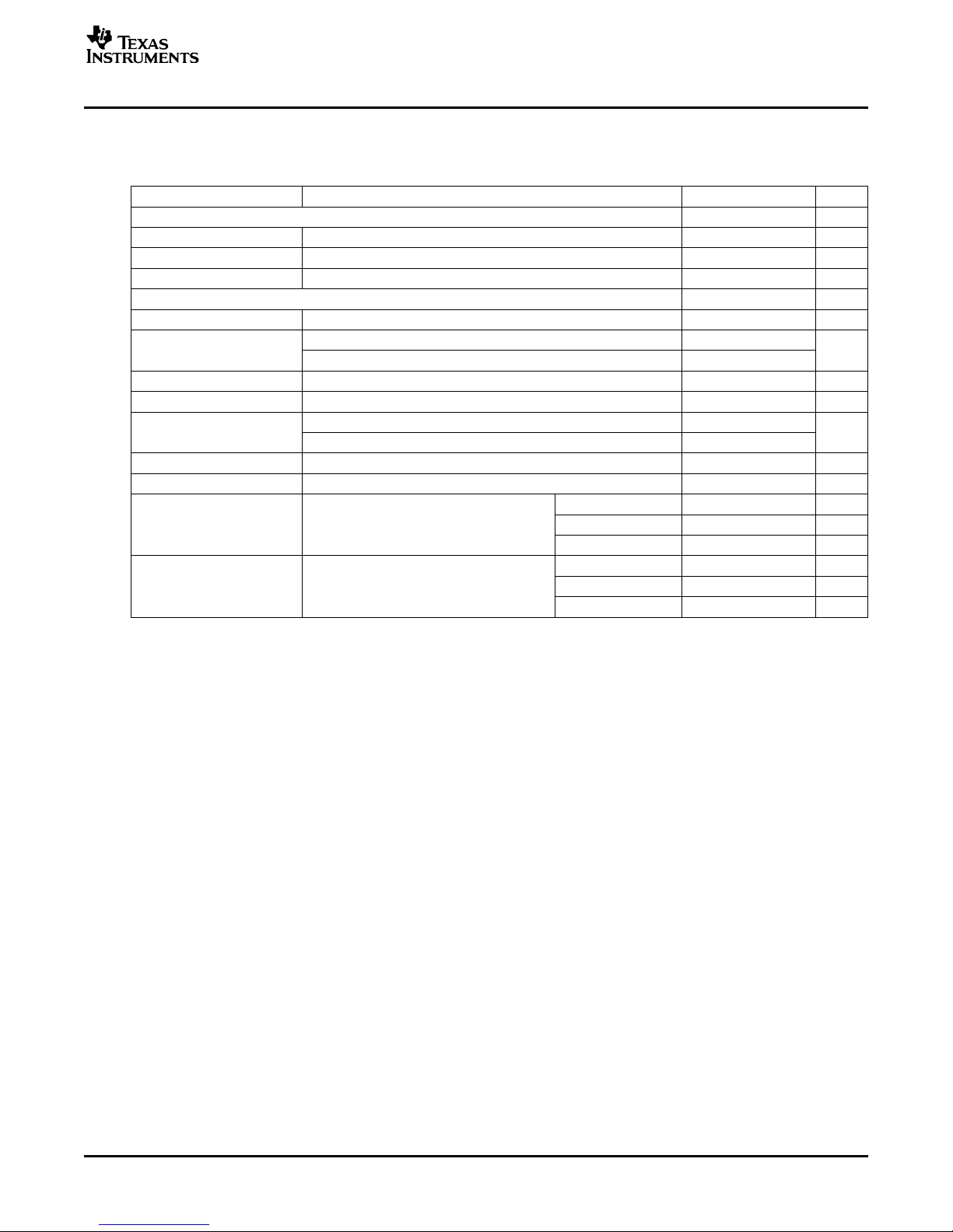
2 TPS40130EVM-001 Electrical Performance Specifications
Table 1. TPS40130EVM-001 Electrical and Performance Specifications
PARAMETER TEST CONDITIONS MIN TYP MAX UNIT
INPUT CHARACTERISTICS
Input voltage range 10 14 V
Max input current VIN= 10 V, I
No-load input current VIN= 14 V, I
OUTPUT CHARACTERISTICS
Output voltage R14 = 8.66 k Ω 1.45 1.50 1.55 V
Output voltage regulation Line regulation (10 V < VIN< 14 V, I
Load regulation (0 A < I
Output voltage ripple VIN= 14 V, I
Output load current 0 40 A
Output overcurrent Limit source current to 8.5 A none —
Limit load current to 40 A
Output current limit Limit source current to VIN= 12 V 80 A
Switching frequency 300 330 360 kHz
Peak efficiency V
Full load efficiency V
= 1.5 V, 20 A < I
OUT
= 1.5 V, I
OUT
TPS40130EVM-001 Electrical Performance Specifications
= 40 A 6.9 A
OUT
= 0 A 180 mA
OUT
= 20 A) 1%
OUT
< 40 A, VIN= 12 V) 1%
OUT
= 40 A 30 mV
OUT
< 30 A V
OUT
= 40 A V
OUT
= 10 V 91%
12V_IN
V
= 12 V 90%
12V_IN
V
= 14 V 89%
12V_IN
= 10 V 89%
12V_IN
V
= 12 V 88%
12V_IN
V
= 14 V 87%
12V_IN
pp
12-V Input, 1.5-V Output, 40-A Two Phase Synchronous Buck Converter Using the TPS40130SLUU208 – October 2004 3
Page 4
www.ti.com
+ + ++ + +
Schematics
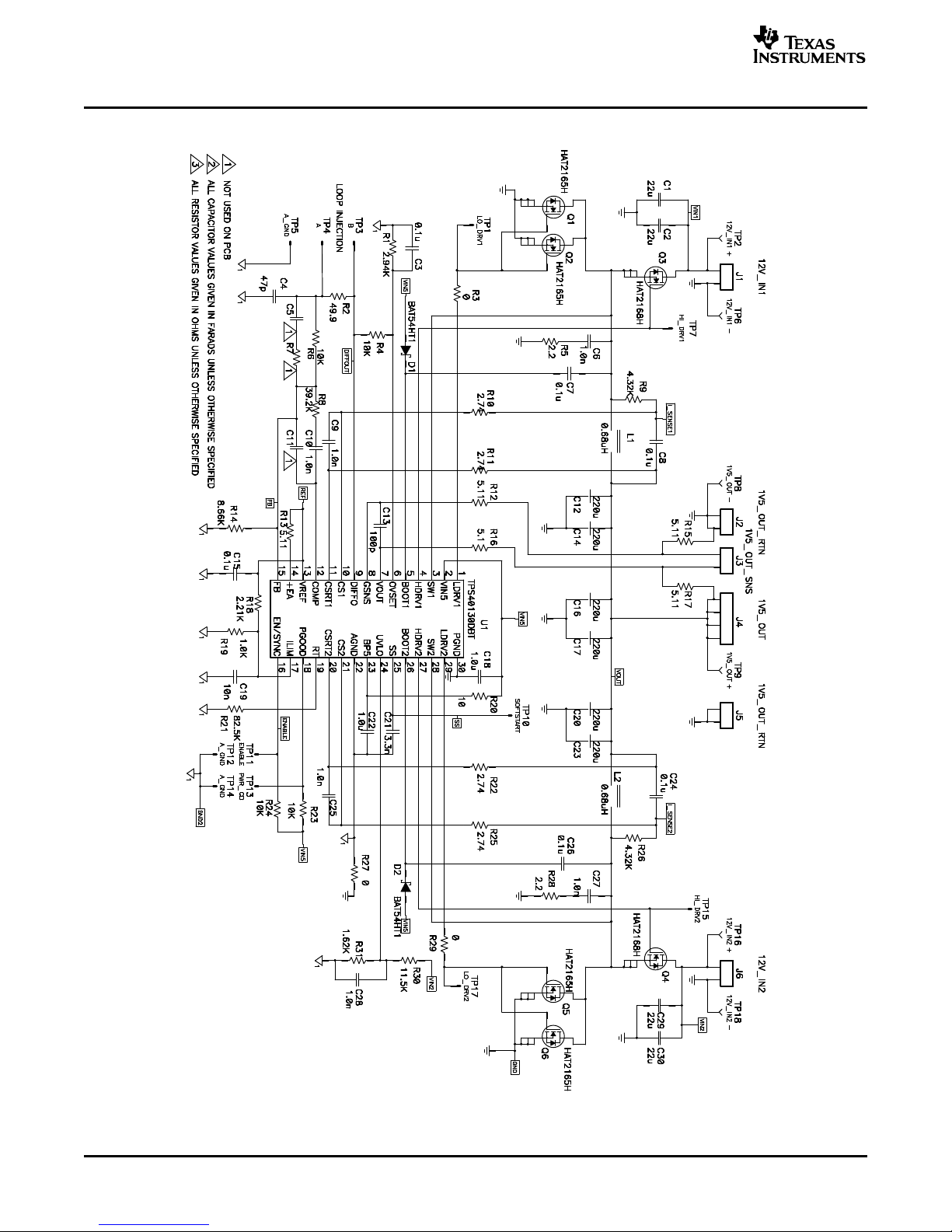
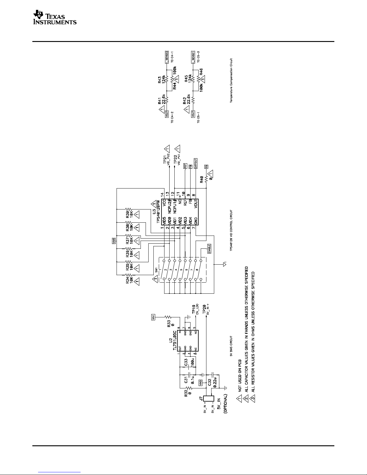
3 Schematics
Figure 1. TPS40130EVM-001 Power Stage/Control Schematic
12-V Input, 1.5-V Output, 40-A Two Phase Synchronous Buck Converter Using the TPS401304 SLUU208 – October 2004
Page 5
www.ti.com
+
Schematics
Figure 2. TPS40130EVM-001 Support Circuitry Schematic
12-V Input, 1.5-V Output, 40-A Two Phase Synchronous Buck Converter Using the TPS40130SLUU208 – October 2004 5
Page 6
www.ti.com
V
VOUT
V
VREF
R14 R6
R14
V
OVP
V
OVSET
R1 R4
R1
Schematics
3.1 Adjusting Output Voltage (R14)
The regulated output voltage can be adjusted within a limited range by changing the ground resistor in the
feedback resistor divider (R14). The output voltage is given by Equation 1 , where V
10.0 k Ω .
Table 2 contains common values for R14 to generate popular output voltages. The TPS40130EVM-001 is
stable through these output voltages but the efficiency may suffer as the power stage is optimized for the
1.5-V output.
= 0.7 V and R6 =
VREF
(1)
3.2 Adjusting Overvoltage Protection (R1)
The output voltage is protected through an overvoltage protection circuit separate from the feedback loop,
to prevent damaging the 4-V output capacitors. Initially set for 3.5 V to allow the user to adjust the output
voltage from 1.2 V to 3.3 V, the OVP set point can be adjusted to be closer to the output voltage by
changing R1. The output overvoltage set point is given by Equation 2 , where V
10.0 k Ω .
Setting R1 = R14 provides 14% to 18% margin between the voltage set value and the OVP set point.
Narrower overvoltage margins can be obtained, however the tolerance on the OVP reference voltage must
be closely observed.
Table 2. Adjusting V
V
OUT
3.3 V 2.67 k Ω
2.5 V 3.83 k Ω
2.2 V 4.64 k Ω
2.0 V 5.36 k Ω
1.8 V 6.34 k Ω
1.5 V 8.66 k Ω
1.2 V 14.0 k Ω
1V5_OUT
With R14
R14
= 0.816 V and R4 =
OVSET
(2)
3.3 Adjusting Overcurrent Protection (I
The TPS40130EVM-001 is preconfigured with the overcurrent protection (OVP) set very high to allow the
converter to deliver high-current, short duration loads, operate under higher loads with sufficient air flow,
but still provide output short-circuit protection. To set the current limit to a lower value, change R19
according to Table 3 .
Table 3. Adjusting Overcurrent Protection with R19
I
MAX CURRENT LIMIT R18 R19
OUT
30 A 40 A 2.21 k Ω 464 Ω
40 A 50 A 2.21 k Ω 590 Ω
50 A 60 A 2.21 k Ω 715 Ω
60 A 70 A 2.21 k Ω 845 Ω
70 A 80 A 2.21 k Ω 1 k Ω
12-V Input, 1.5-V Output, 40-A Two Phase Synchronous Buck Converter Using the TPS401306 SLUU208 – October 2004
)
lim
Page 7

www.ti.com
Test Setup
For more details on setting V
for specific overcurrent protection levels, see the overcurrent protection
Ilim
equations in the Functional Descriptions section of the TPS40130 data sheet.
3.4 Using an External 5-V Supply (R32 and R33)
The TPS40130EVM-001 is designed to be run from a single 12-V supply by incorporating a TL751 5-V
LDO, however an external supply can be used if a separate 5-V bus is available in the target system. To
use an external 5-V supply, connect it through 5V_IN (J7) and remove R32 and R33 to disconnect the
LDO from the circuit. The TPS40130EVM-001 requires approximately 50 mA of current from the 5-V
supply.
4 Test Setup
4.1 Equipment
4.1.1 Voltage Source
V
: The input voltage source (V
4.1.2 Meters
12V_IN
Connect V
to J1 and J6 as shown in Figure 1 .
12V_IN
A1: 0 Adc to 10 Adc ammeter
V1: V
V2: V
, 0 V to 15 V voltmeter
12V_IN
1V5_OUT
VOUT, 0 V to 5 V voltmeter
12V_IN
) should be a 0-V to 15-V variable dc source capable of 8.5 Adc.
4.1.3 Loads
LOAD1: The output load (LOAD1) should be an electronic constant current mode load capable of 0 Adc to
40 Adc at 1.5 V.
4.1.4 Recommended Wire Gauge
V
to J1 and J6: The connection between the source voltage, V
12V_IN
carry as much as 7 Adc. The minimum recommended wire size is AWG #16 with the total length of wire
less than 4 feet (2 feet input, 2 feet return).
J4 to LOAD1: The connection between J4 of HPA087 and LOAD1 can carry as much as 40 Adc. The
minimum recommended wire size is 4 x AWG #16, with the total length of wire less than 1 foot.
J2 and J5 to LOAD1: The connection between J2 and J5 of HPA087 and LOAD1 can carry as much as
40 Adc. The minimum recommended wire size is 2 x AWG #16 (two wires per connector), with the total
length of wire less than 1 foot.
and J1 and J6 of HPA087 can
12V_IN
12-V Input, 1.5-V Output, 40-A Two Phase Synchronous Buck Converter Using the TPS40130SLUU208 – October 2004 7
Page 8

www.ti.com
Test Setup
4.1.5 Other
FAN: The TPS40130EVM-001 includes components that can get hot to the touch. Because this EVM is
not enclosed to allow probing of circuit nodes, a small fan capable of 200 to 400 lfm is required to reduce
component surface temperatures to prevent user injury. The EVM should not be left unattended while
powered or probed while the fan is not running.
OSCILLOSCOPE: A 60-MHz or faster oscilloscope can be used to determine the ripple voltage on
1V5_OUT. The oscilloscope should be set for 1 M Ω impedance, ac coupling, 1 µs/division horizontal
resolution, 20 mV/division vertical resolution for taking output ripple measurements.
4.2 Equipment Setup
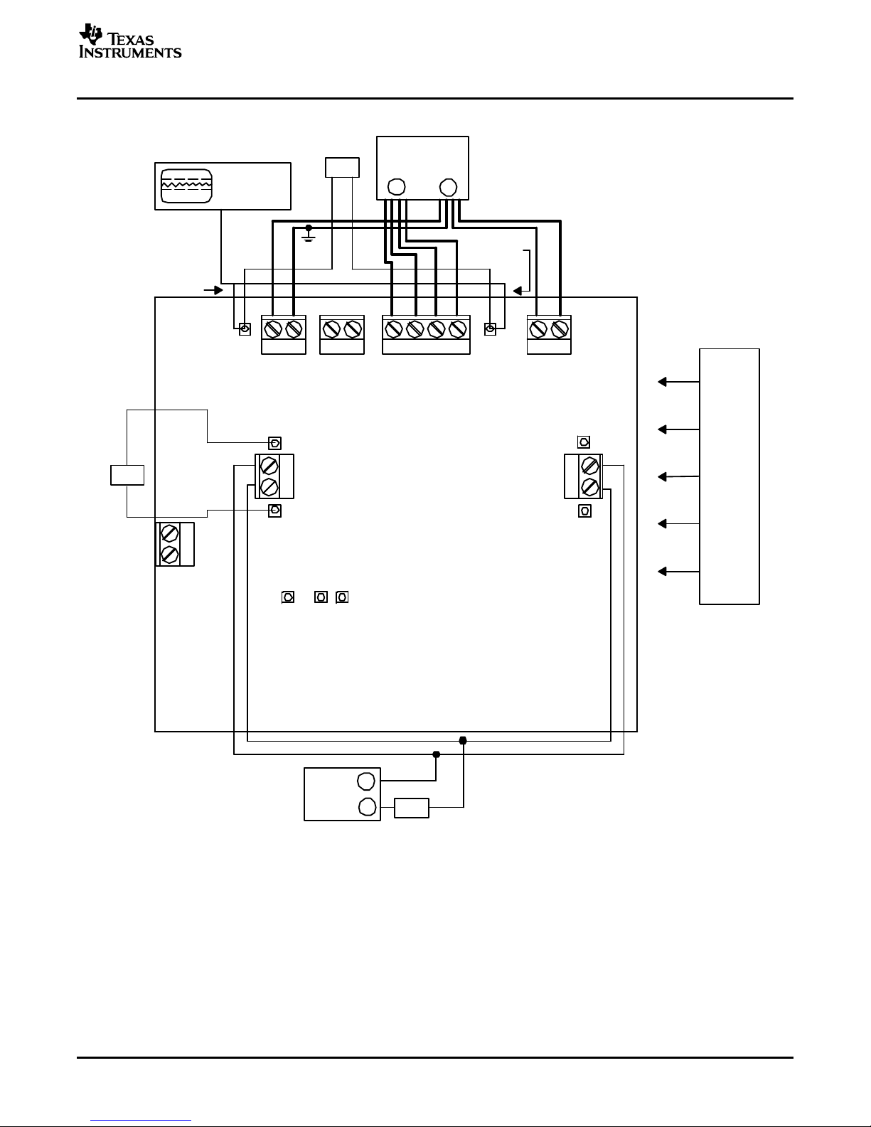
Shown in Figure 3 is the basic test setup recommended to evaluate the TPS40130EVM-001. Note that
although the return for J1, J2, J5, and J6 are all the same, the connections should remain separate as
shown in Figure 3 .
4.2.1 Procedure
1. Working at an ESD workstation, make sure that any wrist straps, bootstraps, or mats are connected
referencing the user to earth ground before power is applied to the EVM. Electrostatic smock and
safety glasses should also be worn.
2. Prior to connecting the dc input source, V
7.0 A maximum. Make sure V
3. Connect the ammeter A1 (0-A to 7-A range) between V
4. Connect voltmeter V1 to 12V_IN + and 12V_IN– as shown in Figure 3 .
5. Connect LOAD1 to J2 as shown in Figure 1 . Set LOAD1 to constant current mode to sink 0 Adc before
V
6. Connect voltmeter, V2 across 1V5_OUT + and 1V5_OUT - as shown in Figure 3 .
7. Place fan as shown in Figure 3 and turn on, making sure air is flowing across the EVM.
, it is advisable to limit the source current from V
12V_IN
is initially set to 0 V and connected as shown in Figure 3 .
12V_IN
and J1 and J2 as shown in Figure 3 .
12V_IN
is applied.
12V_IN
to
12V_IN
12-V Input, 1.5-V Output, 40-A Two Phase Synchronous Buck Converter Using the TPS401308 SLUU208 – October 2004
Page 9
www.ti.com
A1
−
−
+
+
−− −−−
+
++++
−
+
−
+
−
+
V2
1V5_OUT 1V5_OUT_RTN2
12V_IN1
12V_IN2
5V_IN
+
−
−
+
Ground Clip
Oscilloscope
J3 J4 J5
J6
J1
J7
1M, AC
10mV / div
20MHz
LOAD1
1.5V @ 40A
Scope
Probe
1V5_OUT_SNS
1V5_OUT_RTN1
J2
V1
TPS40130EVM−001
Two Phase 12V to 1.5V @ 40A
FAN
V
12V_IN
Test Setup
4.2.2 Diagram
Figure 3. TPS40130EVM-001 Recommended Test Setup
4.3 Startup/Shutdown Procedure
1. Increase V
2. Vary LOAD1 from 0 Adc to 40 Adc
3. Vary V
12V_IN
4. Decrease LOAD1 to 0 A
5. Decrease V
(V1) from 0 Vdc to 10 Vdc
12V_IN
(V1) from 10 Vdc to 14 Vdc
to 0 V
12V_IN
12-V Input, 1.5-V Output, 40-A Two Phase Synchronous Buck Converter Using the TPS40130SLUU208 – October 2004 9
Page 10

www.ti.com
HPA087A Efficiency
80
82
84
86
88
90
92
4 14 24 34
Output Current
Efficiency
Vin 10v
Vin 12v
Vin 14v
Line Regulation
@ 20A Load
1.505
1.507
1.509
1.511
1.513
1.515
10 11 12 13 14
Input Voltage
Output Voltage
Line reg
TPS40130EVM-001 Typical Performance Data and Characteristic Curves
4.4 Equipment Shutdown
1. Shut down oscilloscope
2. Shut down LOAD1
3. Shut down V
12V_IN
4. Shut down fan
5 TPS40130EVM-001 Typical Performance Data and Characteristic Curves
Figure 4 , Figure 5 , Figure 6 , and Figure 7 present typical performance curves for the TPS40130EVM-001.
Since actual performance data can be affected by measurement techniques and environment variables,
these curves are presented for reference and may differ from actual field measurements.
5.1 Efficiency
Figure 4. TPS40130EVM-001 Efficiency, V
5.2 Line Regulation
Figure 5. TPS40130EVM-001 Line Regulation, I
12-V Input, 1.5-V Output, 40-A Two Phase Synchronous Buck Converter Using the TPS4013010 SLUU208 – October 2004
V
1V5_OUT
= 1.5 V, I
= 10 V to 14 V,
12V_IN
1V5_OUT
= 4 A to 40 A
1V5_OUT
= 20 A
Page 11

www.ti.com
5.3 Load Regulation
Load Regulation
1.505
1.507
1.509
1.511
1.513
1.515
0 10 20 30 40
Output Current
OUtput Voltage
10v In
12v In
14v IN
5.4 Transient Response
TPS40130EVM-001 Typical Performance Data and Characteristic Curves
Figure 6. TPS40130EVM-001 Load Regulation
5.4.1 Positive Transient
Figure 7. TPS40130EVM-001 5 A to 55 A Transient Response, 5 A to 55 A at 3 A/µs,
I
1V5_OUT (10A/div)
, V
1V5_OUT(rip)
(20 mv/div), Time 10 µs/div
12-V Input, 1.5-V Output, 40-A Two Phase Synchronous Buck Converter Using the TPS40130SLUU208 – October 2004 11
Page 12

www.ti.com
EVM Assembly Drawings and Layout
5.4.2 Negative Transient
Figure 8. TPS40130EVM-001 55 A to 5 A Transient Response, 55 A to 5 A at 3 A/µs,
I
1V5_OUT (10A/div)
, V
1V5_OUT(rip)
(20 mV/div), Time 10 µs/div
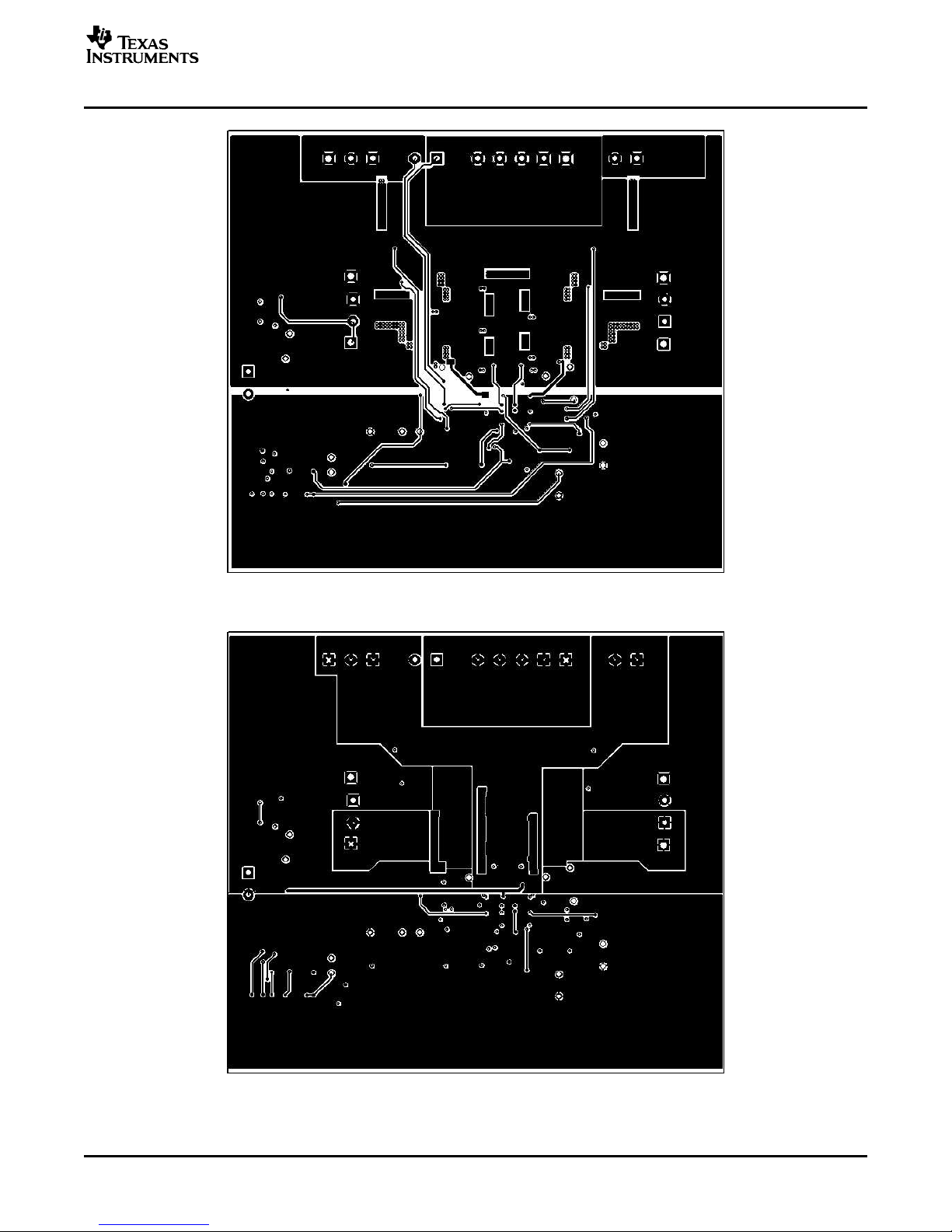
6 EVM Assembly Drawings and Layout
Figure 9 through Figure 14 show the design of the TPS40130EVM-001 printed circuit board. The EVM has
been designed using a 4-layer, 2-oz copper-clad circuit board 4.5" × 4.0” with all components on the top
side to allow the user to easily view, probe, and evaluate the TPS40130 control IC in a practical
application. Moving components to both sides of the PCB or using additional internal layers can offer
additional size reduction for space constrained systems.
12-V Input, 1.5-V Output, 40-A Two Phase Synchronous Buck Converter Using the TPS4013012 SLUU208 – October 2004
Page 13

www.ti.com
EVM Assembly Drawings and Layout
Figure 9. TPS40130EVM-001 Component Placement (Top View)
Figure 10. TPS40130EVM-001 Silkscreen (Top View)
12-V Input, 1.5-V Output, 40-A Two Phase Synchronous Buck Converter Using the TPS40130SLUU208 – October 2004 13
Page 14

www.ti.com
EVM Assembly Drawings and Layout
Figure 11. TPS40130EVM-001 Top Copper (Top View)
Figure 12. TPS40130EVM-001 Layer 2 (X-Ray Top View)
12-V Input, 1.5-V Output, 40-A Two Phase Synchronous Buck Converter Using the TPS4013014 SLUU208 – October 2004
Page 15
www.ti.com
EVM Assembly Drawings and Layout
Figure 13. TPS40130EVM-001 Layer 3 (X-Ray Top View)
Figure 14. TPS40130EVM-001 Bottom Copper (X-Ray Bottom View)
12-V Input, 1.5-V Output, 40-A Two Phase Synchronous Buck Converter Using the TPS40130SLUU208 – October 2004 15
Page 16
www.ti.com
List of Materials
7 List of Materials
Table 4 lists the EVM components as configured according to the schematic shown in Figure 1 and
Figure 2 .
Table 4. TPS40130EVM-001 Bill of Materials
Count RefDes Description Size MFR Part Number
4 C1, C2, C29, Capacitor, ceramic, 22-µF, 16-V, X7R, 15% 1210 TDK C3225X7R1C226M
C30
7 C3, C7, C8, Capacitor, ceramic, 0.1-µF, 25-V, X7R, 10% 805 Std Std
C15, C24,
C26, C31
1 C4 Capacitor, ceramic, 47-pF, 50-V, NPO, 10% 805 Std Std
0 C5, C11 Capacitor, ceramic, pF, 50-V, X7R, 10% 805 Std Std
7 C6, C9, C10, Capacitor, ceramic, 1000-pF, 50-V, X7R, 10% 805 Std Std
C19, C25,
C27, C28
6 C12, C14, Capacitor, aluminum, 220-µF, 5-m Ω , 4-V, 20% 7343 Panasonic EEF-UEOG221R
C16, C17, (UE Series)
C20, C23
1 C13 Capacitor, ceramic, 100-pF, 50-V, NPO, 10% 805 Std Std
2 C18, C22 Capacitor, ceramic, 1-µF, 16-V, X5R, 10% 805 Std Std
1 C21 Capacitor, ceramic, 3300-pF, 50-V, X7R, 10% 805 Std Std
1 C32 Capacitor, ceramic, 0.22-µF, 16-V, X7R, 10% 805 Panasonic ECJ-2VB1C224K
1 C33 Capacitor, POSCAP, 100-µF, 10-V, 40-m Ω , 20% 7343(D) Sanyo 10TPB100ML
2 D1, D2 Diode, Schottky, 200-mA, 30-V SOD323 On Semi BAT54HT1
6 J1, J2, J3, J5, Terminal block, 2-pin, 15-A, 5,1-mm 0.40 x 0.35 OST ED1609
J6, J7
1 J4 Terminal block, 4-pin, 15-A, 5,1-mm 0.80 x 0.35 OST ED2227
2 L1, L2 Inductor, SMT, 0.68-µH, 30-A, 0.9-m Ω 0.524 x 0.492 Wurth S0410124A
4 Q1, Q2, Q5, MOSFET, N-channel, 30-V, 55-A, 2.5-m Ω LFPAK Renesas HAT2165H
Q6
2 Q3, Q4 MOSFET, N-channel, 30-V, 20-A, 6-m Ω LFPAK Renesas HAT2168H
1 R1 Resistor, chip, 2.94-k Ω , 1/10-W, 1% 805 Std Std
4 R10, R11, Resistor, chip, 2.74- Ω , 1/10-W, 1% 805 Std Std
R22, R25
5 R12, R13, Resistor, chip, 5.11- Ω , 1/10-W, 1% 805 Std Std
R15, R16,
R17
1 R14 Resistor, chip, 8.66-k Ω , 1/10-W, 1% 805 Std Std
1 R18 Resistor, chip, 2.21-k Ω , 1/10-W, 1% 805 Std Std
1 R19 Resistor, chip, 1.0-k Ω , 1/10-W, 1% 805 Std Std
1 R2 Resistor, chip, 49.9- Ω , 1/10-W, 1% 805 Std Std
1 R20 Resistor, chip, 10- Ω , 1/10-W, 1% 805 Std Std
1 R21 Resistor, chip, 82.5-k Ω , 1/10-W, 1% 805 Std Std
5 R3, R27, R29, Resistor, chip, 0- Ω jumper, 1/10-W, 5% 805 Std Std
R32, R33
1 R30 Resistor, chip, 11.5-k Ω , 1/10-W, 1% 805 Std Std
1 R31 Resistor, chip, 1.62-k Ω , 1/10-W, 1% 805 Std Std
4 R4, R6, R23, Resistor, chip, 10-k Ω , 1/10-W, 1% 805 Std Std
R24
(1) (2) (3) (4)
(1)
These assemblies are ESD sensitive, ESD precautions shall be observed.
(2)
These assemblies must be clean and free from flux and all contaminants. Use of no clean flux is not acceptable.
(3)
These assemblies must comply with workmanship standards IPC-A-610 Class 2.
(4)
Ref designators marked with an asterik " * " cannot be substituted. All other components can be substituted with equivalent
manufacturers components.
12-V Input, 1.5-V Output, 40-A Two Phase Synchronous Buck Converter Using the TPS4013016 SLUU208 – October 2004
Page 17
www.ti.com
Table 4. TPS40130EVM-001 Bill of Materials (continued)
Count RefDes Description Size MFR Part Number
0 R34, R35, Resistor, chip, 10-k Ω , 1/10-W, 1% 805 Std Std
R36, R37,
R38, R39
0 R40 Resistor, chip, 0- Ω Jumper, 1/10-W, 5% 805 Std Std
0 R41, R42 Resistor, chip, 22.6-k Ω , 1/10-W, 1% 805 Std Std
2 R43, R45 Resistor, chip, 124-k Ω , 1/10-W, 1% 805 Std Std
0 R44, R46 Thermister, chip, NTC, 100-k Ω , -4250 ppm/ ° C 3% 805 Murata NCP21WF104J03RA
2 R5, R28 Resistor, chip, 2.2- Ω , 1/10-W, 1% 805 Std Std
0 R7 Resistor, chip, Ω , 1/10-W, 1% 805 Std Std
1 R8 Resistor, chip, 39.2-k Ω , 1/10-W, 1% 805 Std Std
2 R9, R26 Resistor, chip, 4.32-k Ω , 1/10-W, 1% 805 Std Std
0 SW1 Switch, 8-pos, SPST, low profile, SMT SD08H0SK
11 TP1, TP3, Test point, white, 0.40 hole, 0.050 loop 0.100 Keystone 5002
TP4, TP7,
TP10, TP11,
TP13, TP15,
TP17, TP19,
TP20
0 TP21, TP22 Test point, white, 0.40 hole, 0.050 loop 0.100 Keystone 5002
3 TP2, TP9, Test point, red, thru hole 0.125 Keystone 5010
TP16
3 TP5, TP12, Test point, black, 0.40 hole, 0.050 loop 0.100 Keystone 5001
TP14
3 TP6, TP8, Test point, black, thru hole 0.125 Keystone 5011
TP18
1 U1 IC, High-speed 2-phase synchronous BUCK con- TSSOP-30 TI TPS40130DBT
1 U2 IC, Low drop-out regulator, 5-V to 12-V options SOIC8 TI TL751L05C
0 U3 IC, 6-Bit VID controller SO14 TI TPS40120PW
1 — PCB, 4-Layer FR4, 4.0" x 4.5" x 0.062" 2.4" x 2.1" Any HPA087A
4 — Bumpon
troller
(5)
, transparent 0.44" x 0.2" 3M SJ5303
List of Materials
(5)
Install Bumpons on back side (unpopulated side) of PCB. Install one in each corner after cleaning.
12-V Input, 1.5-V Output, 40-A Two Phase Synchronous Buck Converter Using the TPS40130SLUU208 – October 2004 17
Page 18

IMPORTANT NOTICE
Texas Instruments Incorporated and its subsidiaries (TI) reserve the right to make corrections, modifications,
enhancements, improvements, and other changes to its products and services at any time and to discontinue
any product or service without notice. Customers should obtain the latest relevant information before placing
orders and should verify that such information is current and complete. All products are sold subject to TI’s terms
and conditions of sale supplied at the time of order acknowledgment.
TI warrants performance of its hardware products to the specifications applicable at the time of sale in
accordance with TI’s standard warranty. Testing and other quality control techniques are used to the extent TI
deems necessary to support this warranty . Except where mandated by government requirements, testing of all
parameters of each product is not necessarily performed.
TI assumes no liability for applications assistance or customer product design. Customers are responsible for
their products and applications using TI components. To minimize the risks associated with customer products
and applications, customers should provide adequate design and operating safeguards.
TI does not warrant or represent that any license, either express or implied, is granted under any TI patent right,
copyright, mask work right, or other TI intellectual property right relating to any combination, machine, or process
in which TI products or services are used. Information published by TI regarding third-party products or services
does not constitute a license from TI to use such products or services or a warranty or endorsement thereof.
Use of such information may require a license from a third party under the patents or other intellectual property
of the third party, or a license from TI under the patents or other intellectual property of TI.
Reproduction of information in TI data books or data sheets is permissible only if reproduction is without
alteration and is accompanied by all associated warranties, conditions, limitations, and notices. Reproduction
of this information with alteration is an unfair and deceptive business practice. TI is not responsible or liable for
such altered documentation.
Resale of TI products or services with statements different from or beyond the parameters stated by TI for that
product or service voids all express and any implied warranties for the associated TI product or service and
is an unfair and deceptive business practice. TI is not responsible or liable for any such statements.
Following are URLs where you can obtain information on other Texas Instruments products and application
solutions:
Products Applications
Amplifiers amplifier.ti.com Audio www.ti.com/audio
Data Converters dataconverter.ti.com Automotive www.ti.com/automotive
DSP dsp.ti.com Broadband www.ti.com/broadband
Interface interface.ti.com Digital Control www.ti.com/digitalcontrol
Logic logic.ti.com Military www.ti.com/military
Power Mgmt power.ti.com Optical Networking www.ti.com/opticalnetwork
Microcontrollers microcontroller.ti.com Security www.ti.com/security
Telephony www.ti.com/telephony
Video & Imaging www.ti.com/video
Wireless www.ti.com/wireless
Mailing Address: Texas Instruments
Post Office Box 655303 Dallas, Texas 75265
Copyright 2004, Texas Instruments Incorporated
 Loading...