

Page 1
TPS40100
www.ti.com
MIDRANGE INPUT SYNCHRONOUS BUCK CONTROLLER
WITH ADVANCED SEQUENCING AND OUTPUT MARGINING
FEATURES APPLICATIONS
• Operation over 4.5 V to 18 V Input Range
• Adjustable Frequency (Between 100 kHz and
600 kHz) Current Feedback Control
• Output Voltage Range From 0.7 V to 5.5 V
• Simultaneous, Ratiometric and Sequential
Startup Sequencing
• Adaptive Gate Drive
• Remote Sensing (Via Separate GND/PGND)
• Internal Gate Drivers for N-channel MOSFETs
• Internal 5-V Regulator
• 24-Pin QFN Package
• Thermal Shutdown
• Programmable Overcurrent Protection
• Power Good Indicator
• 1%, 690-mV Reference
• Output Margining, 3% and 5%
• Programmable UVLO (with Programmable
Hysteresis)
• Frequency Synchronization
• Servers
• Networking Equipment
• Cable Modems and Routers
• XDSL Modems and Routers
• Set-Top Boxes
• Telecommunications Equipment
• Power Supply Modules
DESCRIPTION
The TPS40100 is a mid voltage, wide-input (between
4.5 V and 18 V), synchronous, step-down controller.
The TPS40100 offers programmable closed loop
soft-start, programmable UVLO (with programmable
hysteresis), programmable inductor sensed current
limit and can be synchronized to other timebases.
The TPS40100 incorporates MOSFET gate drivers
for external N-channel high-side and synchronous
rectifier (SR) MOSFET. Gate drive logic incorporates
adaptive anti-cross conduction circuitry for improved
efficiency, reducing both cross conduction and diode
conduction in the rectifier MOSFET. The externally
programmable current limit provides a hiccup
overcurrent recovery characteristic.
SLUS601–MAY 2005
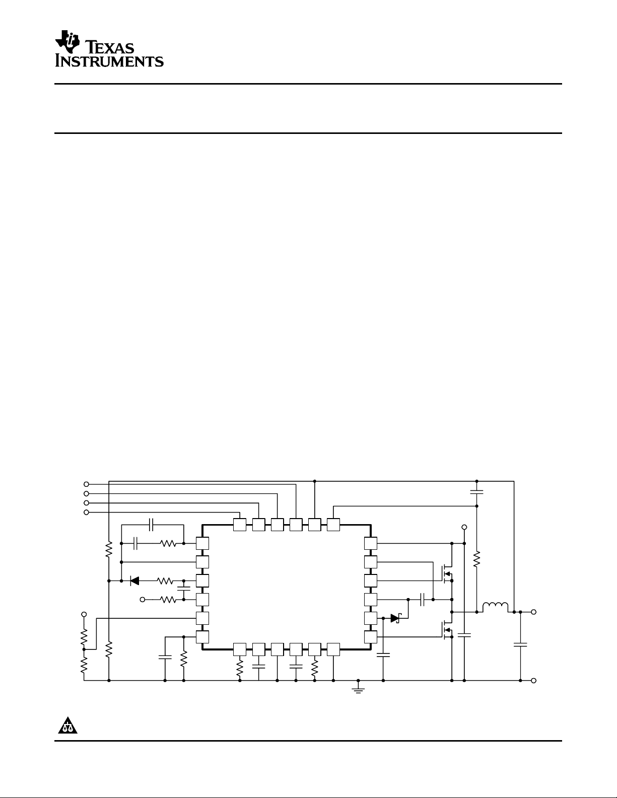
TYPICAL APPLICATION
V
24 2223 21 20 19
PG
SS
VO
GM
VDD
ISNS
HDRV
5VBP
LDRV
PGND
SW
BST
18
17
16
15
14
13
COMP
1
2
3
V
V
IN
TRKIN
Please be aware that an important notice concerning availability, standard warranty, and use in critical applications of Texas
Instruments semiconductor products and disclaimers thereto appears at the end of this data sheet.
4
5
6
MGU
MGD
FB
TRKOUT
TRKIN
UVLO
ILIM
7 98 10 11 12
RT
TPS40100
BIAS
SYNC
GND
IN
UDG−04137
PRODUCTION DATA information is current as of publication date.
Products conform to specifications per the terms of the Texas
Instruments standard warranty. Production processing does not
necessarily include testing of all parameters.
Copyright © 2005, Texas Instruments Incorporated
Page 2
www.ti.com
TPS40100
SLUS601–MAY 2005
ORDERING INFORMATION
T
A
-40°C to 85°C QFN
PACKAGE PART NUMBER
TPS40100RGER
TPS40100RGET
(1) The QFN package (RGE) is available taped and reeled only. Use
large reel device type R (TPS40100RGER) to order quantities of
3,000 per reel. Use small reel device type T (TPS40100RGET) to
order quantities of 250 per reel.
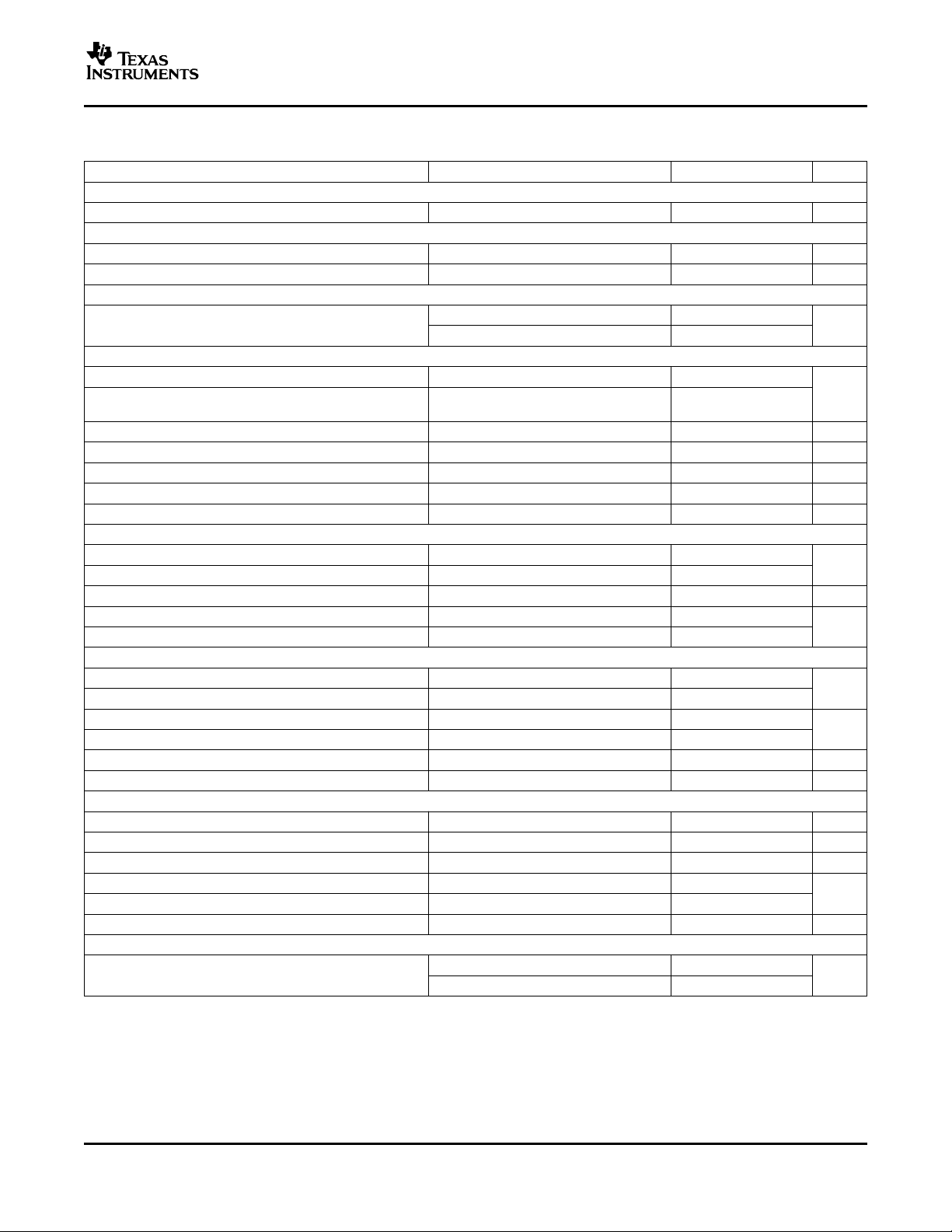
ABSOLUTE MAXIMUM RATINGS
over operating free-air temperature range unless otherwise noted
VDD -0.3to20
5VBP, BIAS, FB, ILIM, ISNS, LDRV, MGU, MGD, PG, SS,
SYNC, UVLO, VO
BST to SW, HDRV to SW
V
Input voltage range V
IN
SW -1.5 to V
SW (transient) < 100 ns -6 to 30
TRKIN -0.3to20
GNDtoPGND -0.3to0.3
TRKOUT -0.3 to 8.0
HDRV, LDRV (RMS) 0.5
HDRV, LDRV (peak) 2.0
FB, COMP, TRKOUT 10 to -10 mA
SS 20 to -20
I
Input current range PG 20
IN
GM 1mA
RT 10
V5BP 50
RT source 100 µA
T
T
Operating junction temperature range –40 to 125
J
Storage temperature –55 to 150
stg
(1) Stresses beyond those listed under "absolute maximum ratings" may cause permanent damage to the device. These are stress ratings
only, and functional operation of the device at these or any other conditions beyond those indicated under "recommended operating
conditions" is not implied. Exposure to absolute-maximum-rated conditions for extended periods may affect device reliability.
(2) BST to SW and HDRV to SW are relative measurements. BST and HDRV can be this amount of voltage above or below the voltage at
SW.
(3) V5BP current includes gate drive current requirements. Observe maximum TJrating for the device.
(2)
(1)
(1)
TPS40100 UNIT
-0.3 to 6
-0.3 to 6.0
VIN
A
(3)
°C
2
Page 3
TPS40100
www.ti.com
SLUS601–MAY 2005
ELECTRICAL CHARACTERISTICS
-40°C ≤ TA=TJ≤ 85°C, V
PARAMETER TEST CONDITIONS MIN TYP MAX UNIT
INPUT VOLTAGE
V
VDD
OPERATING CURRENT
I
DD
I
SD
5VPB
OSCILLATOR/RAMP GENERATOR
f
SW
V
RAMP
t
OFF
D
MIN
t
MIN
V
VLY
FREQUENCY SYNCHRONIZATION
V
IH
V
IL
I
SYNC
t
SYNC
t
SYNC_SH
SOFT-START AND FAULT IDLE
I
SS
I
SS_SINK
V
SSC
V
SSD
V
SSOS
ERROR AMPLIFIER
GBWP Gain bandwidth product
AVOL Open loop 60 80 dB
I
BIAS
I
OH
I
OL
FEEDBACK REFERENCE
V
FB
(1) Ensured by design. Not production tested.
(2) To meet set up time requirements for the synchronization circuit, a negative logic pulse must be greater than 100 ns wide.
Operating range 4.5 18.0 V
Quiescent current VFB> 0.8 V, 0% duty cycle 1.3 1.8 2.5 mA
Shutdown current V
Internal regulator V
Programmable oscillator frequency 100 600
Oscillator frequency accuracy 250 275 300
Ramp amplitude
Fixed off-time 100 150 ns
Minimum duty cycle 0%
Minimum controllable pulse width
Valley voltage
High-level input voltage 2
Low-level input voltage 0.8
Input current, SYNC V
Mimimum pulse width, SYNC 50
Minimum set-up/hold time, SYNC
Soft-start source (charge) current 13 20 25
Soft-start sink (discharge) current 3.4 5.0 6.6
Soft-start completed voltage 3.25 3.40 3.75
Soft-start discharged voltage 0.15 0.20 0.25
Retry interval time to SS time ratio
Offset from SS to error amplifier 300 500 800 mV
Input bias current, FB 50 200 nA
High-level output current 23
Low-level output current 23
Slew rate
Feedback voltage reference mV
=12V,RRT= 182 kΩ,RGM= 232 kΩ,R
VDD
(1)
(1)
(1)
(2)
(1)
(1)
(1)
= 121 kΩ (unless otherwise noted)
ILIM
< 1 V 500 µA
UVLO
7V≤ V
4.5 V ≤ V
4.5 V ≤ V
-40°C ≤ TA=TJ≤ 125°C
≤ 18 V, 0 mA ≤ I
VDD
< 7 V, 0 mA ≤ I
VDD
<18V,
VDD
≤ 30 mA 4.7 5.0 5.3
LOAD
≤ 30 mA 4.3 5.0 5.3
LOAD
0.5 V
C
= 4.7 nF, -40°C ≤ TA=TJ≤ 125°C 175 ns
LOAD
1.0 1.6 2.0 V
= 2.5 V 4.0 5.5 10.0 µA
SYNC
100
16
3.5 5.0 MHz
2.1 V/µs
TA=25°C 686 690 694
-40°C < TA=TJ≤ 125°C 683 697
kHz
P-P
V
ns
µA
V
mA
3
Page 4
www.ti.com
TPS40100
SLUS601–MAY 2005
ELECTRICAL CHARACTERISTICS (continued)
-40°C ≤ TA=TJ≤ 85°C, V
PARAMETER TEST CONDITIONS MIN TYP MAX UNIT
VOLTAGE MARGINING
V
FBMGU
I
MGUP
V
FBMGD
I
MGDN
t
MGDLY
t
MGTRAN
CURRENT SENSE AMPLIFIER
gm
CSA
TC
GM
V
GMLIN
I
ISNS
V
GMCM
CURRENT LIMIT
V
ILIM
t
ILIMDLY
DRIVER SPECIFICATIONS
t
RHDRV
t
FHDRV
I
HDRVSRPKS
I
HDRVSRMIL
I
HSDVSNPK
I
HDRVSNMIL
R
HDRVUP
R
HDRVDN
t
RLDRV
t
FLDRV
I
LDRVSRPK
I
LDRVSNMIL
I
LSDVSNPK
R
LDRVUP
R
LDRVDN
I
SWLEAK
POWERGOOD
V
LPGD
t
PGD
V
LPGDNP
V
OV
V
UV
(3) Margining delay time is the time delay from an assertion of a margining command until the output voltage begins to transition to the
margined voltage.
(4) Ensured by design. Not production tested.
Feedback voltage margin 5% up V
Feedback voltage margin 3% up 2 V ≤ V
Margin-up bias current 60 80 100 µA
Feedback voltage margin 5% down V
Feedback voltage margin 3% down 2 V ≤ V
Margin-down bias current 60 80 100 µA
Margining delay time
Margining transition time 1.5 7.0
Current sense amplifier gain TJ=25°C 300 333 365 µS
Amplifier gain temperature coefficient -2000 ppm/°C
Gm linear range voltage TJ=25°C -50 50 mV
Bias current at ISNS pin VVO=V
Input voltage common mode V
ILIM pin voltage to trip overcurrent 1.44 1.48 1.52 V
Current limit comparator propagation delay HDRV transition from on to off 70 140 ns
HIgh-side driver rise time
HIgh-side driver fall time
HIgh-side driver peak source current
HIgh-side driver source current at 2.5 V
HIgh-side driver peak sink current
High-side driver sink current at 2.5 V
HIgh-side driver pullup resistance I
HIgh-side driver pulldown resistance I
Low-side driver rise time
Low-side driver fall time
Low-side driver peak source current
Low-side driver source current at 2.5 V
Low-side driver peak sink current
Low-side driver sink current at 2.5 V
Low-side driver pullup resistance I
Low-side driver pulldown resistance I
Leakage current from SW pin -1 1 µA
Powergood low voltage I
Powergood delay time 15 25 35 µs
Powergood low voltage , no device power 1.00 1.25 V
Power good overvoltage threshold, V
Power good undervoltage threshold, V
=12V,RRT= 182 kΩ,RGM= 232 kΩ,R
VDD
MGU
MGD
(3)
4.5 V ≤ VIN≤ 5.5 V 0 3.6
(4)
(4)
(4)
(4)
(4)
(4)
(4)
(4)
(4)
(4)
(4)
FB
FB
C
LOAD
C
LOAD
(4)
V
HDRV-VSW
V
HDRV-VSW
HDRV
HDRV
C
LOAD
C
LOAD
V
LDRV
V
LDRV
LDRV
LDRV
PGD
V
VDD
5-V supply
= 121 kΩ (unless otherwise noted)
ILIM
≤ 500 mV 715 725 735
≤ 3 V 700 711 720
MGU
≤ 500 mV 645 655 665
≤ 3 V 660 669 680
MGD
12 30
= 3.3 V 250 nA
ISNS
06
= 4.7 nF 57
= 4.7 nF 47
800
= 2.5 V 700
1.3
= 2.5 V 1.2
= 300 mA 2.4 4.0
= 300 mA 1.0 1.8
= 4.7 nF 57
= 4.7 nF 47
800
= 2.5 V 700
1.3
= 2.5 V 1.2
= 300 mA 2.0 4.0
= 300 mA 0.8 1.5
= 2 mA 30 100 mV
= OPEN, 10-kΩ pullup to external
765
615
mV
mA
ms
ns
mA
A
Ω
ns
mA
A
Ω
mV
4
Page 5

TPS40100
www.ti.com
ELECTRICAL CHARACTERISTICS (continued)
-40°C ≤ TA=TJ≤ 85°C, V
PARAMETER TEST CONDITIONS MIN TYP MAX UNIT
TRACKING AMPLIFIER
V
TRKOS
V
TRKCM
V
TRK
V
HTKROUT
V
LTKROUT
I
SRCTRKOUT
I
SNKTRKOUT
V
TRKDIF
GBWP
AVOL
PROGRAMMABLE UVLO
V
UVLO
I
UVLO
INTERNALLY FIXED UVLO
V
UVLOFON
V
UVLOFOFF
V
UVLOHYST
THERMAL SHUTDOWN
T
SD
T
SDHYST
Tracking amplifier input offset voltage mV
Input common mode, active range 0 6
Tracking amplifier voltage range
High-level output voltage, TRKOUT
Low-level output voltage, TRKOUT 0 0.5
Source current, TRKOUT 0.65 2.00
Sink current, TRKOUT 12
Differential voltage from TRKIN to VO 18 V
Tracking amplifier gain bandwidth product
TRK
Tracking amplifier open loop DC gain
TRK
Undervoltage lockout threshold 1.285 1.332 1.378 V
Hysteresis current 9.0 10.0 10.8 µA
Fixed UVLO turn-on voltage at VDD pin -40°C ≤ TA< 125°C 3.850 4.150 4.425
Fixed UVLO turn-off voltage at VDD pin 3.75 4.06 4.35
UVLO hysteresis at VDD pin 85 mV
Thermal shutdown temerature
Hysteresis
=12V,RRT= 182 kΩ,RGM= 232 kΩ,R
VDD
(6)
(6)
(6)
(6)
V
TRKOS=VTRKIN-VO;VVO
V
TRKOS=VTRKIN-VO
4.5 V ≤ V
5V<V
V
VDD
V
VDD
SLUS601–MAY 2005
= 121 kΩ (unless otherwise noted)
ILIM
≤ 2V 7 25 40
;2V<VVO≤ 6 V -5 25 40
≤ 5.5 V 0 3.6
VDD
VDD
≤ 18 V
(5)
06
= 12 V 5.0 6.5 8.0
= 4.5 V 3.2 3.6
1MHz
60 dB
130 165
25
V
mA
V
°C
(5) Amplifier can track to the lesser of 6 V or (VDD× 0.95)
(6) Ensured by design. Not production tested.
DEVICE INFORMATION
MGU
MGD
SYNC
PG
VO
ISNS
24
23
22
21
20
19
RGE PACKAGE
(BOTTOM VIEW)
COMPFBTRKOUT
TRKIN
UVLO
123456
18 17 16 15 14 13
VDD
SW
BST
HDRV
5VBP
ILIM
7
8
9
10
11
12
LDRV
RT
BIAS
GND
SS
GM
PGND
5
Page 6
www.ti.com
TPS40100
SLUS601–MAY 2005
DEVICE INFORMATION (continued)
TERMINAL FUNCTIONS
TERMINAL
NAME NO.
5VBP 14 O pin to PGND. Power for external circuitry may be drawn from this pin. The total gate drive
BIAS 8 O
BST 15 I connected from 5VBP (A) to BST(K). A schottky diode is recommended for this purpose. A
COMP 1 O
FB 2 I
GM 11 I Connect a resistor from this pin to GND to set the gain of the current sense amplifier.
GND 9 -
HDRV 16 O Floating gate drive for the high side N-channel MOSFET.
ILIM 6 O connected from this pin to GND. When this voltage reaches 1.48 V, an overcurrent condition
ISNS 19 I
LDRV 13 O Gate drive for the N-channel synchronous rectifier.
MGD 23 I 10 kΩ, the output voltage is decreased by 5%. The 3% margin down at the output voltage is
MGU 24 I kΩ, the output voltage is increased by 5%. The 3% margin up at the output voltage is
PG 21 O FB pin is more than 10% higher or lower than 690 mV, a UVLO condition exists, soft-start is
PGND 12 - Power ground for internal drivers
RT 7 I A resistor connected from this pin to GND sets operating frequency.
SS 10 I
SW 17 I
SYNC 22 I synchronize the oscillator frequency to an external master clock. This pin may be left floating
TRKIN 4 I tracks TRKIN voltage with a small controlled offset (typically 25 mV) when the tracking
TRKOUT 3 O the equivalent impedance at the FB node. The diode should be a low leakage type to
UVLO 5 I
VDD 18 I Supply voltage for the device.
VO 20 I
I/O DESCRIPTION
Output of an internal 5-V regulator. A 1-µF bypass capacitor should be connected from this
current and external current draw should not cause the device to exceed thermal capabilities
The bypassed supply for internal device circuitry. Connect a 0.1-µF or greater ceramic
capacitor from this pin to GND.
Gate drive voltage for the high-side N-channel MOSFET. An external diode must be
capacitor must be connected from this pin to the SW pin.
Output of the error amplifier. A feedback network is connected from this pin to the FB pin for
control loop compensation.
Inverting input to the error amplifier. In normal operation the voltage on this pin is equal to
the internal reference voltage (approximately 690 mV).
Low power or signal ground for the device. All signal level circuits should be referenced to
this pin unless otherwise noted.
Current limit pin used to set the overcurrent threshold and transient ride out time. An internal
current source that is proportional to the inductor current sets a voltage on a resistor
is declared by the device. Adding a capacitor in parallel with the resistor to GND sets a time
delay that can be used to help avoid nuisance trips.
Input from the inductor DCR sensing network. This input signal is one of the inputs to the
current sense amplifier for current feedback control and overcurrent protection
Margin down pin used for load stress test. When this pin is pulled to GND through less than
accommodated when this pin is connected to GND through a 30-kΩ resistor.
Margin up pin used for load stress test. When this pin is pulled to GND through less than 10
accommodated when this pin is connected to GND through a 30-kΩ resistor.
Open drain power good output for the device. This pin is pulled low when the voltage at the
active, tracking is active, an overcurrent condition exists or the die is over temperature.
Soft-start programming pin. A capacitor connected from this pin to ground programs the
soft-start time. This pin is also used as a time out function during an overcurrent event.
Connected to the switched node of the converter. This pin is the return line for the flying high
side driver.
Rising edge triggered synchronization input for the device. This pin can be used to
or grounded if the function is not used.
Control input allowing simultaneous startup of multiple controllers. The converter output
amplifier is used. See application secttion for more information.
Output of the tracking amplifier. If the tracking feature is used, this pin should be connected
to FB pin through a resistor in series with a diode. The resistor value can be calculated from
minimize errors due to diode reverse current. For further information on compensation of the
tracking amplifier refer to the application information
Provides for programming the undervoltage lockout level and serves as a shutdown input for
the device.
Output voltage. This is the reference input to the current sense amplifier for current mode
control and overcurrent protection.
6
Page 7

TPS40100
www.ti.com
COMP
FB
MGU
MGD
ISNS
VO
GM
TPS40100
1
2
24
23
19
20
11
SS
Reference
Select
+
Current
Mirror
RT SYNC
7 22
Oscillator
+
0.725 V
0.711 V
0.690 V
0.669 V
0.655 V
+
+
FUNCTIONAL BLOCK DIAGRAM
UVLO
5
CLK
PWM
20 kΩ
+
1.48 V
THERMSD
1.5 V
CLK
OC
1.33 V
10 µA
+
OC/SS
Controller
+
OC
FAULT
CLK
OC
FAULT
UVLO
Adaptive
Drive
Prebias
Control
Reference
Gate
and
Voltages
SLUS601–MAY 2005
15 BST
16 HDRV
17 SW
14 5VBP
13 LDRV
12 PGND
21 PG
TRKOUT
3
4TRKIN
+
6
ILIM
10
SS
9
GND
Housekeeping
8
BIAS
18 VDD
UDG−04142
7
Page 8

www.ti.com
TPS40100
SLUS601–MAY 2005
APPLICATION INFORMATION
Introduction
The TPS40100 is a synchronous buck controller targeted at applications that require sequencing and output
voltage margining features. This controller uses a current feedback mechanism to make loop compensation
easier for loads that can have wide capacitance variations. Current sensing (for both current feedback and
overcurrent) is true differential and can be done using the inductor DC resistance (with a R-C filter) or with a
separate sense resistor in series with the inductor. The overcurrent level is programmable independently from
the amount of current feedback providing greater application flexibility. Likewise, the overcurrent function has
user programmable integration to eliminate nuisance tripping and allow the user to tailor the response to
application requirements. The controller provides an integrated method to margin the output voltage to ± 3% and
± 5% of its nominal value by simply grounding one of two pins directly or through a resistance. Powergood and
clock synchronization functions are provided on dedicated pins. Users can program operating frequency and the
closed loop soft-start time by means of a resistor and capacitor to ground respectively. Output sequencing/tracking can be accomplished in one of three ways: sequential (one output comes up, then a second
comes up), ratiometric (one or more outputs reach regulation at the same time – the voltages all follow a
constant ration while starting) and simultaneous (one or more outputs track together on startup and reach
regulation in order from lowest to highest).
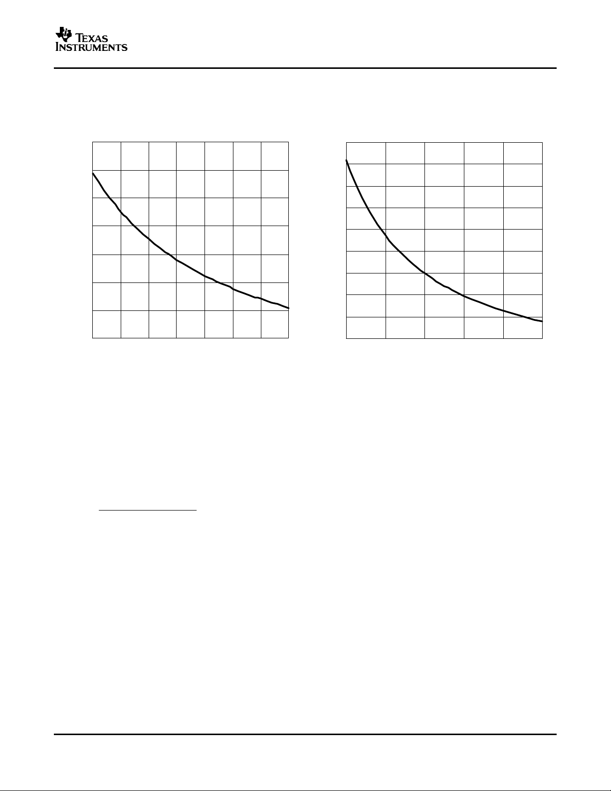
Programming Operating Frequency
Operating frequency is set by connecting a resistor to GND from the RT pin. The relationship is:
ȡ
RT+
where
Figure 1 and Figure 2 show the relationship between the switching frequency and the RTresistor as described in
Equation 1. The scaling is different between them to allow the user a more accurate views at both high and low
frequency.
* 3.98 10
ȧ
f
Ȣ
• fSWis the switching frequency in kHz
• R
SW
is in kΩ
T
ȣ
4
2
ȧ
Ȥ
)
5.14 10
ǒ
f
SW
4
Ǔ
* 8.6 (kW)
(1)
8
Page 9
TPS40100
www.ti.com
APPLICATION INFORMATION (continued)
− Timing Resistance − kΩ
R
T
225
200
175
150
125
100
75
50
250
TIMING RESISTOR TIMING RESISTOR
SWITCHING FREQUENCY SWITCHING FREQUENCY
(250 kHz to 600 kHz) (100 kHz to 350 kHz)
350300 400 500450 600550
f
− Switching Frequency − kHz
SW
vs vs
Figure 1. Figure 2.
SLUS601–MAY 2005
550
500
450
400
350
300
250
− Timing Resistance − kΩ
T
200
R
150
100
100
150 200 250 350300
f − Switching Frequency − kHz
Selecting an Inductor Value
The inductor value determines the ripple current in the output capacitors and has an effect on the achievable
transient response. A large inductance decreases ripple current and output voltage ripple, but is physically larger
than a smaller inductance at the same current rating and limits output current slew rate more that a smaller
inductance would. A lower inductance increases ripple current and output voltage ripple, but is physically smaller
than a larger inductance at the same current rating. For most applications, a good compromise is selecting an
inductance value that gives a ripple current between 20% and 30% of the full load current of the converter. The
required inductance for a given ripple current can be found from:
L +
ǒ
VIN* V
VIN fSW DI
OUT
Ǔ
V
OUT
(H)
(2)
where
• L is the inductance value (H)
• V
is the input voltage to the converter (V)
IN
• V
• f
•∆I is the peak-to-peak ripple current in the inductor (A)
is the output voltage of the converter (V)
OUT
is the switching frequency chosen for the converter (Hz)
SW
Selecting the Output Capacitance
The required value for the output capacitance depends on the output ripple voltage requirements and the ripple
current in the inductor, as well as any load transient specifications that may exist.
The output voltage ripple depends directly on the ripple current and is affected by two parameters from the
output capacitor: total capacitance and the capacitors equivalent series resistance (ESR). The output ripple
voltage (worst case) can be found from:
9
Page 10

www.ti.com
TPS40100
SLUS601–MAY 2005
APPLICATION INFORMATION (continued)
DV + DI
ESR ) ǒ
ƪ
8 C
1
OUT
f
SW
Ǔ
(V)
ƫ
(3)
where
•∆V is the peak to peak output ripple voltage (V)
•∆I is the peak-to-peak ripple current in the inductor (A)
• f
is the switching frequency chosen for the converter (Hz)
SW
• C
• ESR is the equivalent series resistance of the capacitor, C
is the capacitance value of the output capacitor (F)
OUT
OUT
(Ω)
For electrolytic capacitors, the output ripple voltage is almost entirely (90% or more) due to the ESR of the
capacitor. When using ceramic output capacitors, the output ripple contribution from ESR is much smaller and
the capacitance value itself becomes more significant. Paralleling output capacitors to achieve a desired output
capacitance generally lowers the effective ESR more effectively than using a single larger capacitor. This
increases performance at the expense of board area.
If there are load transient requirements that must be met, the overshoot and undershoot of the output voltage
must be considered. If the load suddenly increases, the output voltage momentarily dips until the c urrent in the
inductor can ramp up to match the new load requirement. If the feedback loop is designed aggressively, this
undershoot can be minimized. For a given undershoot specification, the required output capacitance can be
found by:
C
O(under)
+
2 V
UNDER
L I
D
STEP
ǒVIN* V
MAX
2
(F)
Ǔ
OUT
(4)
where
• C
• L is the inductor value (H)
• I
STEP
• V
• D
• V
• V
is the output capacitance required to meet the undershoot specification (F)
O(under)
is the change in load current (A)
is the maximum allowable output voltage undershoot
UNDER
is the maximum duty cycle for the converter
MAX
is the input voltage
IN
is the output voltage
OUT
Similarly, if the load current suddenly goes from a high value to a low value, the output voltage overshoots. The
ouput voltage rises until the current in the inductor drops to the new load current. The required capacitance for a
given amount of overshoot can be found by:
C
O(over)
+
2 V
L I
OVER
STEP
V
2
OUT
(F)
(5)
where
• C
• L in the inductor value (H)
• I
• V
• V
The required value of output capacitance is the maximum of C
is the output capacitance required to meet the undershoot specification (F)
O(over)
is the change in load current (A)
STEP
is the maximum allowable output voltage overshoot
OVER
is the output voltage
OUT
O(under)
and C
O(over)
.
Knowing the inductor ripple current, the switching frequency, the required load step and the allowable output
voltage excursion allows calculation of the required output capacitance from a transient response perspective.
The actual value and type of output capacitance is the one that satisfies both the ripple and transient
specifications.
10
Page 11
TPS40100
www.ti.com
SLUS601–MAY 2005
APPLICATION INFORMATION (continued)
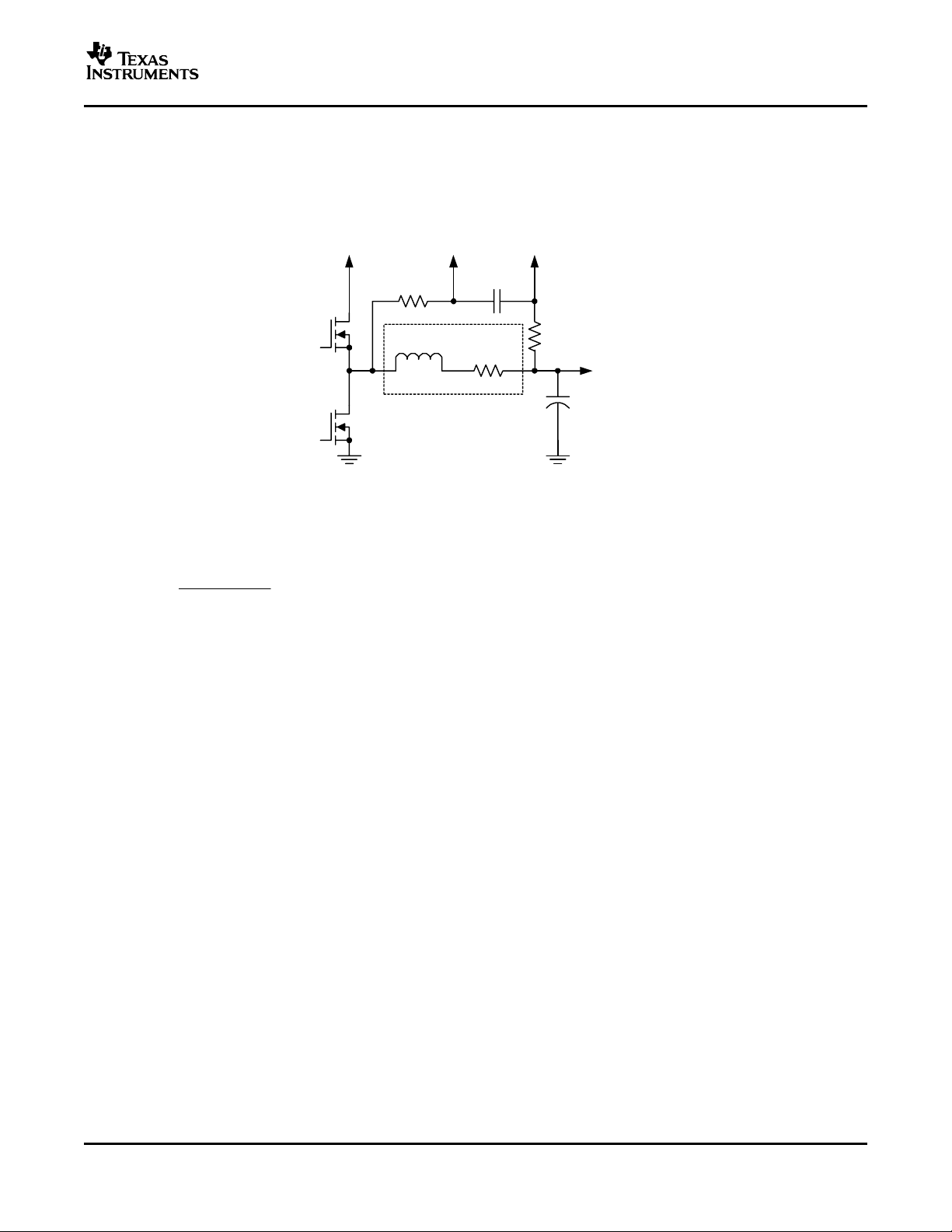
Calculating the Current Sense Filter Network
The TPS 40100 gets current feedback information by sensing the voltage across the inductor resistance, R
order to do this, a filter must be constructed that allows the sensed voltage to be representative of the actual
current in the inductor. This filter is a series R-C network connected across the inductor as shown in Figure 3.
V
IN
To ISNS pin
R
FLT
L
R
C
LDC
FLT
To VO pin
100 Ω
V
O
C
O
UDG−04150
Figure 3. Current Sensing Filter Circuit
If the R
FLT-CFLT
voltage across R
condition (100 nF is suggested). R
R
FLT
time constant is matched to the L/R
. It is recommended to keep R
+
LDC
L
R
C
LDC
* 100 (W)
FLT
can then be calculated.
FLT
time constant, the voltage across C
LDC
10 kΩ or less. C
FLT
can be arbitrarily chosen to meet this
FLT
is equal to the
FLT
where
• R
• C
• L is the output inductance (H)
• R
When laying out the board, better performance can be accomplished by locating C
is the current sense filter resistance (Ω)
FLT
is the current sense filter capacitance (F)
FLT
is the DC resistance of the output inductor (Ω)
LDC
as close as possible to the
FLT
VO and ISNS pins. The closer the two resistors can be brought to the device the better as this reduces the
length of high impedance runs that are susceptible to noise pickup. The 100-Ω resistor from V
to the VO pin
OUT
of the device is to limit current in the event that the output voltage dips below ground when a short is applied to
the output of the converter.
LDC
.In
(6)
Compensation for Inductor Resistance Change Over Temperature
The resistance in the inductor that is sensed is the resistance of the copper winding. This value changes over
temperature and has approximately a 4000 ppm/°C temperature coefficient. The gain of current sense amplifier
in the TPS40100 has a built in temperature coefficient of approximately -2000 ppm/°C. If the circuit is physically
arranged so that there is good thermal coupling between the inductor and the device, the thermal shifts tend to
offset. If the thermal coupling is perfect, the net temperature coefficient is 2000 ppm/°C. If the coupling is not
perfect, the net temperature coefficient lies between 2000 ppm/°C and 4000 ppm/°C. For most applications this is
sufficient. If desired, the temperature drifts can be compensated for. The following compensation scheme
assumes that the temperature rise at the device is directly proportional to the temperature rise at the inductor. If
this is not the case, compensation accuracy suffers. Also, there is generally a time lag in the temperature rise at
the device vs. at the inductor that could introduce transient errors beyond those predicted by the compensation.
Also, the 100-Ω resistor in Figure 3 is not shown. However, it is required if the output voltage can dip below
ground during fault conditions. The calculations are not afffected, other than increasing the effective value of R
by 100-Ω.
F1
11
Page 12

www.ti.com
TPS40100
SLUS601–MAY 2005
APPLICATION INFORMATION (continued)
The relative resistance change in the inductor is given by:
R
+ 1 ) TCL ǒTL* T
REL(L)
where
• R
• TCLis the temperature coefficient of copper, 4000 ppm/°C or 0.004
• T
• T
is the relative resistance of the inductor at TLcompared to the resistance at T
REL(L)
is the inductor copper temperature (°C)
L
is the reference temperature, typically lowest ambient (°C)
BASE
The relative gain of the current sense amplifier is given by a similar equation:
gm
+ 1 ) TCGM ǒTIC* T
(REL)
where
• gm
• TCGMis the temperature coefficient of the amplifier gain, -2000 ppm/°C or -0.002
• T
• T
is the relative gain of the amplifier at TICcompared to the gain at T
REL
is the device junction temperature (°C)
IC
is the reference temperature, typically lowest ambient (°C)
BASE
The temperature rise of the device can usually be related to the temperature rise of the inductor. The relationship
between the two temperature rises can be approximated as a linear relationship in most cases:
TIC* T
BASE
+ǒTL* T
BASE
where
• TICis the device junction temperature (°C)
• T
• T
• k
is the reference temperature, typically lowest ambient (°C)
BASE
is the inductor copper temperature (°C)
L
is the constant that relates device temperature rise to the inductor temperature rise and must be
THM
determined experimentally for any given design
BASE
Ǔ
k
Ǔ
(dimensionless)
Ǔ
BASE
THM
(dimensionless)
(7)
BASE
(8)
BASE
(9)
With these assumptions, the effective inductor resistance over temperature is:
R
REL(eff)
R
REL(eff)
+ R
REL(L)
gm
+ƪ1 ) TC
REL
ǒ
TL* T
L
is the relative effective resistance that must be compensated for when doing the compensation. The
BASE
Ǔƫ
ƪ1 ) k
TCGM ǒTL* T
THM
BASE
Ǔƫ
(dimensionless)
circuit of Figure 4 shows a method of compensating for thermal shifts in current limit. The NTC thermistor (R
must be well coupled to the inductor. C
should be located as close to the device as possible.
FLT
(10)
NTC
)
12
Page 13

TPS40100
www.ti.com
APPLICATION INFORMATION (continued)
ILIM
6
R
ILIM
+
−2000 ppm/°C
V
IN
VO
20
ISNS
19
R
SLUS601–MAY 2005
R
THE
R
F3
R
F2
R
NTC
C
F1
L
FLT
R
LDG
V
OUT
C
OUT
UDG−04148
Figure 4. Compensation for Temperature Coefficient of the Inductor Resistance
The first step is to determine an attenuation ratio α. This ratio should be near to 1 but not too close. I f it is too
close to 1, the circuit requires large impedances and thermistor values too high. If α is too low, the current signal
is attenuated unnecessarily. A suggested value is 0.8.
R
a ^ 0.8
R
is the equivalent resistance of the RF2-RF3-R
THE
R
+ RF2)
THE
The base temperature (T
THE
R
) R
THE
RF3 R
RF3) R
(dimensionless)
F1
network:
NTC
NTC
(W)
NTC
) should be selected to be the lowest temperature of interest for the thermal
BASE
(11)
(12)
matching – the lowest ambient expected. The resistance of the inductor at this base temperature should be used
to calculate effective resistance. The expected current sense amplifier gain at T
calculating over current components (R
ILIM
).
should be used for
BASE
The next step is to decide at what two temperatures the compensation is matched to the response of the
deviceand inductor copper, T1 and T2. Once these are chosen, an NTC thermistor can be chosen and its value
found from its data sheet at these two temperatures: R
NTC(T1)
and R
. The component values in the network
NTC(T2)
can be calculated using the following equations:
13
Page 14

www.ti.com
TPS40100
SLUS601–MAY 2005
APPLICATION INFORMATION (continued)
LDC(Tbase)
LDC(Tbase)
a R
R
LDC(T1)
a R
R
LDC(T2)
NTC(T1)
THE(T1)
) R
R
L
FLT
LDC(Tbase)
* a R
LDC(Tbase)
* a R
* R
* R
NTC(T2)
NTC(T2)
a
R
R
NTC(T2)
THE(T2)
(W)
(W2)
(W)
REL(effT1)
REL(effT2)
R
LDC(Tbase)
R
LDC(Tbase)
(W)
(W)
F1
F1
(dimensionless)
(W)
(W)
Ǹ
2a
ǒRF3) R
is the value of the current sense filter capacitor (F)
is the DC resistance of the inductor at temperature T
(W)
Ǔ
NTC(T1)
RF3) R
are the equivalent resistances of the R
are the inductor resistances at temperatures T1 and T2
, are the relative resistances of the inductor at T1 and T2 vs. Tbase
are the effective resistance of the NTC thermistor at temperatures T1 and T2
* RF3 R
NTC(T1)
RF1+
R
R
R
R
LDC(T1)
LDC(T2)
THE(T1)
THE(T2)
R
LDC(Tbase) C
+ R
+ R
+
+
R
a + 1 *
b + R
c + R
RF3+
RF2+
R
NTC(T1)
NTC(T1)
* b " b2* 4ac
R
THE(T1)
where
• L is the value of the output inductance (H)
• C
FLT
•αis the attenuation ratio chosen from Equation 11
• R
THE(T1),RTHE(T2)
• R
LDC(Tbase)
• R
LDC(T1),RLDC(T2)
• R
REL(effT1),RREL(effT2)
• R
NCT(T1),RNTC(T2)
NTC(T1)
(W)
network at temperatures T1 and T2
THE
in Ω
BASE
(13)
(14)
(15)
(16)
(17)
(18)
(19)
(20)
(21)
(22)
Establishing Current Feedback
The amount of current feedback in a given application is programmable by the user. The amount of current
feedback used is intended to be just enough to reduce the Q of the output filter double pole. This allows design
of a converter control loop that is stable for a very wide range of output capacitance. Setting the current feedback
higher offers little real benefit and can actually degrade load transient response, as well as introduce pulse
skipping in the converter. The current feedback is adjusted by setting the gain of the current sense amplifier. The
amplifier is a transconductance type and its gain is a set by connecting a resistor from the GM pin to GND:
RGM+
43.443 gm
2
) 0.01543 gm
CSA
where
• RGMis the resistor that sets the gain of the amplifier (Ω)
• gm
is the gain of the current sense amplifier (S)
CSA
The value of the sense amplifier gain should be less than 1000 µS, and more than 250 µS, with the resulting
gain setting resistor greater than 50 kΩ. As a suggested starting point, set the gain of the current sense amplifier
to a nominal 280 µS with RGM of 279 kΩ. This value should accommodate most applications adequately.
Figure 5 shows the current sense amplifier gain setting resistance vs. the sense amplifier gain.
14
3
) 3.225 10
CSA
*6
(W)
(23)
Page 15

TPS40100
www.ti.com
APPLICATION INFORMATION (continued)
CURRENT SENSE AMPLIFIER GAIN SETTING RESISTANCE
CURRENT SENSE AMPLIFIER GAIN
75
25
250 400 700550 1000850
gm − Sense Amplifier Transconductance − µS
− Gain Setting Resistance − kΩ
R
325
275
225
175
125
GM
SLUS601–MAY 2005
vs
Figure 5.
Control to Output Gain of the Converter
A model that gives a good first order approximation to the control to output gain of a converter based on the
TPS40100 controller is shown in Figure 6. This model can be used in conjunction with a simulator to generate ac
and transient response plots. The block labeled “X2” is a simple gain of 2. The amplifier gm can be a simple
voltage controlled current source with a gain equal to the selected gm for the current sense amplifier (CSA).
Analytically, the control to output gain of this model ( Figure 6) can be expressed as follows:
KCO(s) +
K
(s) is the output filter transfer function:
FILT
K
(s) =
FILT
R
LOAD
R
) R
LDC
VIN K
1 ) Y(s) KCS K
LOAD
L C
R
(dimensionless)
Usually, R
K
FILT
LDC
(s) +
<< R
L C
and the following approximation holds:
LOAD
OUT
Y(s) is the current signal transfer function and assumes that the inductor intrinsic time constant is matched to the
current sense filter network time constant.
K
PWM
PWM
OUT)RLOAD
LDC)RLOAD
s2)
ƪ
(s)
FILT
V
s2)
R
ESR
L)R
LOAD COUT
(dimensionless)
IN
L)C
C
OUT
R
R
ESR
ǒR
OUT
s ) 1
ǒR
LOAD
C
LOAD RESR)RLDC RLOAD)RLDC RESR
ESR)RLDC
OUT
s ) 1
R
LOAD
Ǔ
ƫ
s ) 1
(24)
Ǔ
s ) 1
(25)
(26)
15
Page 16

www.ti.com
TPS40100
SLUS601–MAY 2005
APPLICATION INFORMATION (continued)
Y(s) +
1 * K
L
R
LDC
KCSis the gain of the current sense amplifier in the current feedback loop:
KCS+ gm
CSA
where (for Equation 24 through Equation 28)
• VINis the input voltage (V)
• K
PWM
• R
LOAD
• R
LDC
• L is the output filter inductance (H)
• C
OUT
• R
ESR
• gm
CSA
• 20 kΩ is the impedance the current sense amplifier works against (from block diagram)
A computer aided math tool is highly recommended for use in evaluating these equations.
(s)
FILT
(dimensionless)
s ) 1
20 kW (dimensionless)
is the gain of the pulse width modulator and is equal to 2
is the equivalent load resistance (Ω)
is the DC inductor resistance (Ω)
is the output filter capacitance (F)
is the equivalent series resistance of the output filter capacitor (Ω)
is the gain of the current sense amplifier (S)
(27)
(28)
L
R
LDC
V
IN
+
X2
R
EA
20 kΩ
gm
CSA
+
R
COMP
2
R
ISNS
FLT
C
FLT
VO
C
1
C
2
FB
+
+
690 mV
R
C
OUT
R
ESR
R
BIAS
1
V
X
V
OUT
R
LOAD
1 V AC
UDG−04149
Figure 6. Averaged Model for a Converter Based on the TPS40100
Compensating the Loop (Type II)
The first step is to select a target loop crossover frequency. Choosing the crossover frequency too high
contributes to making the converter pulse skip. A balance of crossover frequency and amount of current
feedback must be maintained to avoid pulse skipping. A suggested maximum loop crossover frequency is one
fifth-of the switching frequency.
f
SW
fCv
where
• fCis the loop crossover frequency
• f
(Hz)
5
is the switching frequency
SW
(29)
16
Page 17

TPS40100
www.ti.com
SLUS601–MAY 2005
APPLICATION INFORMATION (continued)
Using either the analytical model or the simulated model, determine the control to output gain at the chosen loop
crossover frequency. The gain of the compensator is the reciprocal of this gain:
K
COMP(co)
where
• K
COMP(CO)
• K
CO(fC
If simulating the response using the model, the control to output gain is VX/V
over the range of interest and plot VX/V
Depending on the chosen loop crossover frequency and the characteristics of the output capacitor, either a Type
II or a Type III compensator could be required. If the output capacitance has sufficient ESR, phase shift from the
ESR zero may by used to eliminate the need for a Type III compensator. The model in Figure 6 uses a Type II
compensator. In this case the compensator response looks like Figure 7.
1
+
Ť
KCO(fc)
(Hz)
Ť
is the required compensator gain at the crossover frequency
) is the value of the control to output transfer function at the crossover frequency
. Sweep the AC voltage source
OUT
OUT
.
COMPENSATOR GAIN
vs
FREQUENCY
(30)
K
COMP(co)
Gain − dB
f
Z
f − Frequency − kHz
f
C
Figure 7.
f
P
First select R1. The choice is somewhat arbitrary but affects the rest of the components once chosen. The
suggested value is 10 kΩ.
R
is found from the gain required from the compensator at the crossover frequency.
2
R2+ KLF R1(W)
(31)
It is generally recommended to place the pole frequency one decade above the crossover frequency and the
zero frequency one decade below the crossover frequency.
17
Page 18

www.ti.com
TPS40100
SLUS601–MAY 2005
APPLICATION INFORMATION (continued)
fP+ fC 10 +
f
C
fZ+
10
+
2 p R2 C
2 p R
Compensating the Loop (Type III)
If the output capacitor does not have sufficient ESR to use the phase shift from the ESR zero, a Type III
compensator is required. This is the case for most designs with ceramic output capacitors only. A series R-C
circuit is added in parallel to R1as shown in Figure 8.
This is the same compensator as in Figure 6 except for the addition of C3and R3. A typical response of this
circuit is shown in Figure 9.
1
1
C
2
2
1
(Hz)
(Hz)
(32)
(33)
Gain − dB
COMPENSATOR GAIN
K
COMP(co)
K
LF
f
Z
f − Frequency − kHz
vs
FREQUENCY
R
BIAS
C
3
R
1
C
1
C
2
K
HF
f
Z3
Figure 9. Figure 8. Type III Compensator Schematic
f
f
C
f
P3
P
COMP
Error Amplifier
R
2
FB
+
R
3
VX
UDG−04143
The reason for using the Type III compensator is to take advantage of the phase lead associated with the
upward slope of the gain between f
and fP3. The crossover frequency should be located between these two
Z3
frequencies. The amount of phase lead generated is dependent on the separation of the fZ3and fP3. In general, if
f
is one half of fCand fP3is twice fC, the amount of phase lead at fCgenerated is sufficient for most applications.
Z3
Certainly more or less may be used depending on the situation.
As an example of selecting the extra required extra phase lead, suppose that the control to output gain phase
evaluates to -145° at fC. The Type II compensator has approximately 11.5° of phase lag at fCdue to the origin
pole, the zero at f
/10 and the pole at 10xfC. This would give only 23.5° of phase margin, which while stable is
C
not ideal. Placing fZ3and fP3at one half and twice the crossover frequency respectively adds approximately 36°
of phase lead at f
for a new phase margin of 59.5°.
C
To calculate the values for this type of compensator, first select R1. Again the choice is somewhat arbitrary. 10
kΩ is a suggested value.
18
Page 19

TPS40100
www.ti.com
SLUS601–MAY 2005
APPLICATION INFORMATION (continued)
Select the required extra phase lead beyond the Type II compensation to obtain the required phase margin and
calculate the required multiple for the additional pole and zero:
K3+ tanǒQ
LEAD
Ǔ
) tanǒQ
where
•Θ
• K
is the required extra phase lead to be generated by the addition of the extra pole and zero
LEAD
is the multiplier applied to fCto get the new pole and zero locations
3
The locations of fZ3and fP3are:
f
fZ3+
C
(Hz)
K
3
fP3+ fC K3(Hz)
where
• K3is the multiplier applied to fCto get the new pole and zero locations
• f
is the zero created by the addition of R3and C
Z3
• fP3is the pole created by the addition of R3and C
The required gain, K
COMP(co)
, from the compensator at fC, is the same as for the Type II compensation, found in
Equation 30. The gain KLF(see Figure 9) is found by:
K
KLF+
COMP(co)
K
3
(dimensionless)
R2can then be found:
R2+ KLF R1(W)
The high-frequency gain is:
KHF+ K
COMP(co)
K3(dimensionless)
Ǔ
) 1Ǹ(dimensionless)
LEAD
(34)
(35)
(36)
3
3
(37)
(38)
(39)
Now:
R3+
KHF R1* R
C3+
2 p R3 f
R1 R
2
1
P3
(W)
2
(40)
(F)
(41)
The remaining pole and zero are located a decade above and below fCas before. Equation 31 and Equation 32
canbeusedtosolveforC1and C2as before.
19
Page 20

www.ti.com
TPS40100
SLUS601–MAY 2005
APPLICATION INFORMATION (continued)
Establishing Tracking and Designing a Tracking Control Loop
The tracking startup feature of the TPS40100 is a separate control loop that controls the output voltage to a
reference applied to the TRKIN pin. This reference voltage is typically a ramp generated by an external R-C
circuit. Connecting the junction of R5, C5 and R6 (see Figure 10) of multiple converters together allows the
converters output voltages to track together during start up. A controlled power down is accomplished by pulling
down the common junction in a controlled manner and then removing power to the converters or turning them off
by grounding the UVLO pin.The relevant circuit fragment is shown in Figure 10.
V
OUT
A
R
3
R
1
V
IN
R
6
R
C
5
VO
20
TRKIN
5
4
TRKOUT
+
C
4
3
C
3
R
D
4
1
R
A
BIAS
C
2
FB
2
690 mV
C
1
R
2
COMP
+
1
To PWM
UDG−04145
Figure 10. Tracking Loop Control Schematic
First, select a value for R4. In order for this circuit to work properly, the output of the tracking amplifier must be
able to cause the FB pin to reach at least 690 mV with the output voltage at zero volts. This is so that the output
voltage can be forced to zero by the tracking amplifier. This places a maximum value on R4:
R4t
ƪ
V
HTRKOUT(min)
* V
V
FB
DIODE
* V
FB
ƫ
R1 R
R1) R
BIAS
BIAS
W
(42)
where
• V
HTRKOUT(min)
• V
DIODE
• VFBis the value of the reference voltage (690 mV)
is the minimum output voltage of the tracking amplifier (see Electrical Characteristics table)
is the forward voltage of the device selected for D
1
R4should not be chosen much lower than this value since that unnecessarily increases tracking loop gain,
making compensation more difficult and opening the door to potential non-linear control issues. D1 could be a
schottky if the impedance of the R
1-RBIAS
string is low enough that the leakage current is not a consequence. Be
aware that schottky diode leakage currents rise significantly at elevated temperature. If elevated temperature
operation and increased accuracy are important, use a standard or low leakage junction diode or the
base-emitter junction of a transistor for D1.
Once R4is selected, the gain of the closed loop power supply looking into “A” is known. That gain is the ratio of
R1and R4:
dV
dV
OUT
TRKOUT
+*
R
1
(dimensionless)
R
4
(43)
The tracking loop itself should have a crossover frequency much less that the crossover frequency of the voltage
control loop. Typically, the tracking loop crossover frequency is 1/10th or less of the voltage loop crossover
frequency to avoid loop interactions. Note that the presence of the diode in the circuit gives a non-linear control
mechanism for the tracking loop. The presence of this non-linearity makes designing a control loop more
challenging. The simplest approach is to simply limit the bandwidth of this loop to no more than necessary.
20
Page 21

TPS40100
www.ti.com
SLUS601–MAY 2005
APPLICATION INFORMATION (continued)
Knowing the gain of the voltage loop looking into R4and the desired tracking loop crossover frequency, R5and
C4can be found:
R
R5 C4+
2 p R1 f
where
• f
is the desired tracking loop crossover frequency
CTRK
The actual values of R5and C4are a balance between impedance level and component size. Any of a range of
values is applicable. In general, R5should be no more than 20% of R6, and less than 10 kΩ. If this is done, then
R6can safely be ignored for purposes of tracking loop gain calculations. For general usage, R6should probably
be between 100 kΩ and 500 kΩ.
If an overshoot bump is present on the output at the beginning a tracking controlled startup, the tracking loop
bandwidth is likely too high. Reducing the bandwidth helps reduce the initial overshoot. See Figure 11 and
Figure 12.
4
cTRK
(s)
(44)
(200 mV/div)
t − Time − 1 ms/div
Figure 11. Excessive Tracking Loop Bandwidth Figure 12. Limited Tracking Loop Bandwidth
The tracking ramp time is the time required for C5to charge to the same voltage as the output voltage of the
converter.
V
OUT
t
+*R6 C5 lnǒ1 *
TRK
Ǔ
V
(s)
IN
(45)
where
• V
• V
• t
is the output voltage of the converter
OUT
is the voltage applied to the top of R
IN
is the desired tracking ramp time
TRK
6
With these equations, it is possible to design the tracking loop so that the impedance level of the loop and the
component size are balanced for the particular application. Note that higher impedances make the loop more
susceptible to noise issues while lower impedances require increased capacitor size.
Figure 13 shows the spice model for the voltage loop expanded for use with the tracking loop.
21
Page 22

www.ti.com
TPS40100
SLUS601–MAY 2005
APPLICATION INFORMATION (continued)
V
+
IN
X2
gm
CSA
ISNS
+
R
C
SFLT
1
L
R
C
LDC
SFLT
R
C
OUT
CESR
R
V
OUT
LOAD
R
EA
20 kΩ
R
R
3
BIAS
R
C
2
2
+
+
R
4
C4
C
3
R
1
V
X
+
R
5
+
UDG−04147
Figure 13. AC Behavioral Model for Tracking Control Loop
To use the model, the AC voltage source is swept over the frequency range of interest. The open loop ac
response is VX/V
OUT
.
Programming Soft-Start Time
The soft-start time of the TPS40100 is fully user programmable by selecting a single capacitor. The SS pin
sources 20 µA to charge this capacitor. The actual output ramp-up time is the amount of time that it takes for the
20 µA to charge the capacitor through a 690 mV range. There is some initial lag due to an offset from the actual
SS pin voltage to the voltage applied to the error amplifier. See Figure 15. The soft-start is done in a closed loop
fashion, meaning that the error amplifier controls the output voltage at all times during the soft start period and
the feedback loop is never open as occurs in duty cycle limit soft-start schemes. The error amplifier has two
non-inverting inputs, one connected to the 690 mV reference voltage, and one connected to the offset SS pin
voltage. The lower of these two voltages is what the error amplifier controls the FB pin to. As the voltage on the
SS pin ramps up past approximately 1.04 V (resulting in 690 mV at the SS “+” input – See Figure 15), the 690
mV reference voltage becomes the dominant input and the converter has reached its final regulation voltage.
The capacitor required for a given soft-start ramp time for the output voltage is given by:
CSS+ TSS
where
• TSSis the desired soft-start ramp time (s)
• C
• V
20 mA
is the required capacitance on the SS pin (F)
SS
is the reference voltage feedback loop (690 mV)
FB
F
V
FB
(46)
22
Page 23

TPS40100
www.ti.com
APPLICATION INFORMATION (continued)
COMP
1
FB
2
SS
10
C
SS
Figure 14. Error Amplifier and Soft-Start Functional Diagram
20 µA
350 mV
+
5 µA
690 mV
+
+
Error Amplifier
SLUS601–MAY 2005
COMP
CHARGE
From UVLO circuits,
Fault controller
UDG−04138
UVLO
(Internal Logic State)
4.8 V
3.5 V
1.04 V
0.35 V
SS
Tss
Tss Delay
VOUT
PDG
Figure 15. Relationship Between UVLO (Internal Logic State), SS, VOUT and PGD at Startup
Interaction Between Soft-Start and Tracking Startup
Since the TPS40100 provides two means of controlling the startup (closed loop soft-start and tracking) care must
be taken to ensure that the two methods do not interfere with each other. The two methods should not be
allowed to try and control the output at the same time. If tracking is to be used, the reference input to the tracking
amplifier (TRKIN) should be held low until soft-start completes, or the voltage at the SS pin is at least above 1.04
V. This ensures that the soft-start circuit is not trying to control the startup at the same time as tracking circuit. If
it is desired to have soft-start control the startup, then there are two options:
23
Page 24

www.ti.com
TPS40100
SLUS601–MAY 2005
APPLICATION INFORMATION (continued)
• Disconnect the tracking amplifier output from the FB node (this is the recommended solution. The tracking
amplifier can then be used for other system purposes if desired)
• Maintain the tracking amplifier output connection to the FB circuit - the reference to the tracking amplifier
should be tied to VDD pin in this case. This places the tracking amplifier output (TRKOUT) in a low state
continuously and therefore removes any influence the tracking circuit has on the converter startup.
Additionally, when tracking is allowed to control the startup, soft-start should not be set to an arbitrarily short
time. This causes the output voltage to bump up when power is applied to the converter as soft-start ramps up
quickly and the tracking loop (which is necessarily low bandwidth) cannot respond fast enough to control the
output to zero voltage. In other words, the soft start ramp rate must be within the capability of the tracking loop to
override.
Overcurrent Protection
Overcurrent characteristics are determined by connecting a parallel R-C network from the ILIM pin to GND. The
ILIM pin sources a current that is proportional to the current sense amplifier transconductance and the voltage
between ISNS and VO. This current produces a voltage on the R-C network at ILIM. If the voltage at the ILIM pin
reaches 1.48 V, an overcurrent condition is declared and the outputs stop switching for a period of time. This
time period is determined by the time is takes to discharge the soft-start capacitor with a controlled current sink.
To set the overcurrent level:
V
R
+
ILIM
gm
CSA
where
• V
ILIM
• I
is the overcurrent level to be set
OC
• gm
CSA
• R
LDC
• R
ILIM
The response time of the overcurrent circuit is determined by the R-C time constant at the ILIM pin and the level
of the overcurrent. The response time is given by:
tOC+*R
ILIM
where
• tOCis the response time before declaring an overcurrent
• R
ILIM
• n is the multiplier of the overcurrent. If the overcurrent is 2 times the programmed level, then n is 2.
ILIM
R
is the overcurrent comparator threshold (1.48 V typically)
is the transconductance of the current sensing amplifier
is the equivalent series resistance of the inductor (or the sense resistor value)
is the value of the resistor from ILIM to GND
C
(Ω) and C
I
LDC
lnǒ1 *
ILIM
(F) are the components connected to the ILIM pin
ILIM
OC
W
1
Ǔ
(s)
n
(47)
(48)
By suitable manipulation of the time constant at ILIM, the overcurrent response can be tailored to ride out short
term transients and still provide protection for overloads and short circuits. The gm of the current sense amplifier
has a temperature coefficient of approximately -2000 ppm/°C. This is to help offset the temperature coefficient of
resistance of the copper in the inductor, about +4000 ppm/°C. The net is a +2000 ppm/°C temperature
coefficient. So, for a 100°C increase in temperature, the overcurrent threshold decreases by 20%, assuming
good thermal coupling between the controller and the inductor. Temperature compensation can be done as
described earlier if desired.
When an overcurrent condition is declared, the controller stops switching and turns off both the high-side
MOSFET and the low-side MOSFET. The soft-start capacitor is then discharged at 25% of the charge rate during
an overcurrent condition and the converter remains idle until the soft start pin reaches 200 mV, at which point the
soft-start circuit starts charging again and the converter attempts to restart. In normal operation, the soft-start
capacitor is charged to approximately 3.5 V when an initial fault is applied to the output. This means that the
minimum time before the first restart attempt is:
24
Page 25

TPS40100
www.ti.com
SLUS601–MAY 2005
APPLICATION INFORMATION (continued)
t
RESTART
+
where
3.3 C
• t
RESTART
• C
• I
is soft start capacitance (F)
SS
is the soft start discharge current – 5 µA
SSDIS
If the output fault is persistent, and an overcurrent is declared on the restart, both of the MOSFETs are turned off
and the soft-start capacitor continues to charge to 3.5 V and then discharge to 200 mV before another restart is
attempted.
SS
I
SSDIS
(s)
is the initial restart time (s)
(49)
UVLO Programming
The TPS40100 provides the user with programmable UVLO level and programmable hysteresis. The UVLO
detection circuit schematic is described in Figure 16 from a functional perspective.
R
1
UVLO 1.33 V
5
R
2
10 µA
+
UVLO
TPS40100
UDG−04139
Figure 16. UVLO Circuit Functional Diagram
To program this circuit, first select the amount of hysteresis (the difference between the startup voltage and the
shutdown voltage) desired:
V
R1+
HYST
I
UVLO
W
(50)
Then select the turn-on voltage and solve for R2.
R2+
V
VON* V
UVLO
UVLO
R
1
* R1 I
UVLO
W
(51)
where
• V
• I
• V
is the desired level of hysteresis in the programmable UVLO circuit
HYST
is the undervoltage lockout circuit hysteresis current (10 µA typ)
UVLO
is the UVLO comparator threshold voltage (1.33 V typ)
UVLO
25
Page 26

www.ti.com
TPS40100
SLUS601–MAY 2005
APPLICATION INFORMATION (continued)
Voltage Margining
The TPS40100 allows the user to make the output voltage temporarily be 3% above or below the nominal output,
or 5% above or below the nominal output. This is accomplished by connecting the MGU or MGD pins to GND
directly or through a resistance. See Table 1.
Table 1. Output Voltage Margining States
RESISTANCE TO GND (kΩ)
R
MGU
OPEN OPEN Nominal
<10 OPEN +5%
OPEN < 10 -5%
25 to 37 OPEN +3%
OPEN 25 to 37 -3%
R
MGD
There are some important considerations when adjusting the output voltage.
• Only one of these pins should be anything other than an open circuit at any given time. States not listed in
the table are invalid states and the behavior of the circuit may be erratic if this is tried.
• When changing the output voltage using the margin pins, it is very important to let the margin transition
complete before altering the state of the margin pins again.
• Do not use mechanical means (switches, non-wetted relay contacts, etc) to alter the margining state. The
contact bounce causes erratic behavior.
OUTPUT VOLTAGE
Synchronization
The TPS40100 may be synchronized to an external clock source that is faster than the free running frequency of
the circuit. The SYNC pin is a rising edge sensitive trigger to the oscillator that causes the current cycle to
terminate and starts the next switching cycle. It is recommended that the synchronization frequency be no more
than 120% of the free running frequency. Following this guideline leads to fewer noise and jitter problems with
the pulse width modulator in the device. The circuit can be synchronized to higher multiples of the free running
frequency, but be aware that this results in a proportional decrease in the amplitude of the ramp from the
oscillator applied to the PWM, leading to increased noise sensitivity and increased PWM gain, possibly affecting
control loop stability.
The pulse applied to the SYNC pin can be any duty ratio as long as the pulse either high or low is at least 100 ns
wide. Levels are logic compatible with any voltage under 1 V considered a low and any voltage over 2 V
considered a high.
Power Good Indication
The PGD pin is an open drain output that actively pulls to GND if any of the following conditions are met
(assuming that the input voltage is above 4.5V)
• Soft-start is active (VSS<3.5V)
• Tracking is active (V
TRKOUT
• VFB<0.61V
• VFB>0.77V
• V
UVLO
<1.33V
• Overcurrent condition exists
• Die temperature is greater than 165°C
A short filter (20 µs) must be overcome before PGD pulls to GND from a high state to allow for short transient
conditions and noise and not indicate a power NOT good condition.
The PGD pin attempts to pull low in the absence of input power. If the VDD pin is open circuited, the voltage on
PGD typically behaves as shown in Figure 17.
>0.7V)
26
Page 27

TPS40100
www.ti.com
POWERGOOD VOLTAGE
vs
2.5
2.0
1.5
1.0
− Powergood Voltage − V
PGD
0.5
V
0
012345
POWERGOOD CURRENT
V
= 0 V
VDD
I
− Powergood Current − mA
PGD
Figure 17.
SLUS601–MAY 2005
Pre-Bias Operation
Some applications require that the converter not sink current during startup if a pre-existing voltage exists at the
output. Since synchronous buck converters inherently sink current some method of overcoming this characteristic
must be employed. Applications that require this operation are typically power rails for a multiple supply
processor or ASIC. The method used in this controller, is to not allow the low side or rectifier FET to turn on until
there the output voltage commanded by the start up ramp is higher than the pre-existing output voltage. This is
detected by monitoring the internal pulse width modulator (PWM) for its first output pulse. Since this controller
uses a closed loop startup, the first output pulse from the PWM does not occur until the output voltage is
commanded to be higher than the pre-existing voltage. This effectively limits the controller to sourcing current
only during the startup sequence. If the pre-existing voltage is higher that the intended regulation point for the
output of the converter, the converter starts and sinks current when the soft-start time has completed.
Remote Sense
The TPS 40100 is capable of remotely sensing the load voltage to improve load regulation. This is accomplished
by connecting the GND pin of the device and the feedback voltage divider as near to the load as possible.
CAUTION:
Long distance runs for the GND pin will cause erratic controller behavior.
This begins to appear as increased pulse width jitter. As a starting point, the GND pin connection should be no
further than six inches from the PGND connection. The actual distance that starts causing erratic behavior is
application and layout dependent and must be evaluated on an individual basis. If the controller exhibits output
pulse jitter in excess of 25 ns and the GND pin is tied to the load ground, connecting the GND pin closer to the
PGND pin (and thereby sacrificing some load regulation) may improve performance. In either case, connecting
the feedback voltage divider at the point of load should not cause any problems. For layout, the voltage divider
components should be close to the device and a trace can be run from there to the load point.
27
Page 28

www.ti.com
TPS40100
SLUS601–MAY 2005
Application Schematics
2
Margin up 3%
2N7002
12 V
100 kΩ
1 µF
Margin down 3% Power Good Indication
27 kΩ
2N7002
V
OUT
Connect at load
10 kΩ
200 kΩ
40.2 kΩ
13.7 kΩ
27 kΩ
47 pF
300 pF
30 kΩ
MMBD1501A
4.99 kΩ
100 pF
14.3 kΩ
158 kΩ
24 2223 21 20 19
MGU
MGD
1
COMP
2
FB
3
TRKOUT
47 nF
4
TRKIN
5
UVLO
6
ILIM
RT
BIAS
7 98 10 11 12
TPS40100
SYNC
GND
PG
SS
3.3 V to 5 V logic supply or 5VBP pin
VO
ISNS
18
VDD
SW
HDRV
BST
5VBP
LDRV
GM
17
16
15
14
13
PGND
270 kΩ
Si73444DP
100 nF
BAT54
Si7868DP
1 µF
5.9 kΩ
100 nF
1.0 µH
COEV
DXM1306−1R0
1.7 mΩ (typ)
470 µF
Panasonic
EEF−SEOD471R
1 1
V
OUT
1.2 V
15 A
12 V
1 µF
162 kΩ
22 µF TDK C4532X7R1C226M
1
Open switch after input power is stable and SS capacitor had finished charging.
2
150 nF
10 nF
(if required)
10 Ω
BAT54S
(if required)
Figure 18. 300-kHz, 12-V to 1.2-V Converter With Tracking Startup Capability and Remote Sensing
Remote
GND Sense
Connect at
Load
UDG−04140
28
Page 29

TPS40100
www.ti.com
3
Margin down 5%
Margin up 5%
2N7002
3.32 kΩ
12 V
330 pF
100 kΩ
1 µF 2.67 kΩ
V
OUT
Connect at load
200 kΩ
40.2 kΩ
2N7002
10 kΩ
47 pF
3.9 nF
15 kΩ
MMBD1501A
4.99 kΩ
100 pF
Power Good Indication
6.2 kΩ
1
2
3
47 nF
4
5
6
158 kΩ
24 2223 21 20 19
PG
SS
VO
VDD
SW
HDRV
BST
5VBP
LDRV
GM
MGU
MGD
SYNC
COMP
FB
TRKOUT
TPS40100
TRKIN
UVLO
ILIM
RT
BIAS
GND
7 98 10 11 12
3.3 V to 5 V logic supply or 5VBP pin
ISNS
18
17
16
15
14
13
PGND
Si7344DP
100 nF
BAT54
Si7868DP
1 µF
5.9 kΩ
100 nF
1.0 µH
COEV
DXM1306−1R0
1.7 mΩ (typ)
1
SLUS601–MAY 2005
12 V
2
2 2
1
V
OUT
3.3 V
15 A
1
22 µF TDK C4532X7R1C226M
100 µF TDK C3225X5ROJ107M
2
Open switch after input power is stable and SS capacitor had finished charging.
3
120 kΩ 1 µF 270 kΩ
150 nF
Figure 19. 400-kHz, 12-V to 3.3-V Converter With Tracking Capability and 5% Margining
UDG−04141
29
Page 30

www.ti.com
TPS40100
SLUS601–MAY 2005
12 V
200 kΩ
40.2 kΩ
10 kΩ
13.7 kΩ
300 pF
100 pF
47 pF
14.3 kΩ
NC
NC
158 kΩ
NC NC NC NC
24 2223 21 20 19
MGU
MGD
1
COMP
2
FB
3
TRKOUT
TPS40100
4
TRKIN
5
UVLO
6
ILIM
RT
BIAS
7 98 10 11 12
SYNC
GND
PG
SS
VO
VDD
SW
HDRV
BST
5VBP
LDRV
GM
ISNS
18
17
16
15
14
13
PGND
270 kΩ
Si73444DP
100 nF
BAT54
Si7868DP
1 µF
5.9 kΩ
DXM1306−1R0
100 nF
1 µH
COEV
1.7 mΩ (typ)
Panasonic
EEF−SEOD471R
11
470 µF
12 V
V
OUT
1.2 V
15 A
187 kΩ 1 µF
150 nF
1
Figure 20. Minimal Application for 12-V to 1-V Converter
22 µF TDK C4532X7R1C226M
UDG−05063
30
Page 31

TPS40100
www.ti.com
12 V
10 kΩ
300 pF
200 kΩ
40.2 kΩ 13.7 kΩ
47 pF
100 pF
14.3 kΩ
NC
NC
NC NC
24 2223 21 20 19
MGU
MGD
1
COMP
2
FB
3
TRKOUT
TPS40100
4
TRKIN
5
UVLO
6
ILIM
RT
BIAS
7 98 10 11 12
158 kΩ
187 kΩ
1 µF
SYNC
GND
150 nF
PG
SS
VO
VDD
SW
HDRV
BST
5VBP
LDRV
GM
ISNS
18
17
16
15
14
13
PGND
270 kΩ
Si73444DP
100 nF
BAT54
Si7868DP
1 µF
100 nF
5.9 kΩ
1 µH
COEV
DXM1306−1R0
1.7 mΩ (typ)
1
1
12 V
470 µF
Panasonic
EEF−SEOD471R
External 5 V
SLUS601–MAY 2005
V
OUT
1.2 V
15 A
10 kΩ
External
Clock
50%
Duty
NC NC
24 2223 21 20 19
MGU
MGD
COMP
1
FB
2
TRKOUT
3
TRKIN
4
UVLO
5
ILIM
6
RT
BIAS
7 98 10 11 12
120 kΩ
1 µF
SYNC
TPS40100
GND
150 nF
PG
SS
VO
VDD
SW
HDRV
BST
5VBP
LDRV
GM
270 kΩ
ISNS
18
17
16
15
14
13
PGND
Si7344DP
100 nF
BAT54
Si7868DP
1 µF
22 µF TDK C4532X7R1C226M
1
100 µF TDK C3225X5ROJ107M
2
5.9 kΩ
DZM1306−1R
1
3.32 kΩ
330 pF
12 V
200 kΩ
40.2 kΩ
10 kΩ
2.67 kΩ
3.9 nF
100 pF
470 pF
6.2 kΩ
NC
NC
158 kΩ
Figure 21. Sequenced Supplies, With Oscillators 180 Degrees Out of Phase
100 nF
1 µH
COEV
3 mΩ (typ)
1
2
12 V
2
Power
Good
V
3.3 V
15 A
2
UDG−05064
OUT
31
Page 32

www.ti.com
TPS40100
SLUS601–MAY 2005
External Clock,
50% duty
12 V
47 kΩ
12 V
200 kΩ
40.2 kΩ
10 kΩ
300 pF
MMBD1501A
13.7 kΩ
3.32 kΩ
330 pF
12 V
200 kΩ
47 pF
14.3 kΩ
30 kΩ
4.99 kΩ
100 pF
47 nF
158 kΩ
10 kΩ
470 pF
3.9 nF
MMBD1501A
4.99 kΩ
NC NC
24 2223 21 20 19
MGU
MGD
1
COMP
2
FB
3
TRKOUT
4
TRKIN
UVLO
5
ILIM
6
RT
7 98 10 11 12
187 kΩ
6.2 kΩ
15 kΩ
SYNC
TPS40100
BIAS
GND
150 nF
1 µF
NC NC
24 2223 21 20 19
MGU
1
COMP
2
FB
3
TRKOUT
47 nF
4
TRKIN
PG
SS
MGD
VO
ISNS
VDD
SW
HDRV
BST
5VBP
LDRV
GM
PGND
SYNC
TPS40100
18
17
16
15
14
13
270 kΩ
PG
Si73444DP
100 nF
BAT54
Si7868DP
VO
VDD
SW
HDRV
BST
ISNS
18
17
16
15
1 µF
5.9 kΩ
EEF−SEOD471R
1 1
Si7344DP
100 nF
100 nF
470 µF
Panasonic
10 kΩ
470 µF
Panasonic
EEF−SEOD471R
5.9 kΩ
100 nF
1 µH
COEV
DZM1306−1R
3 mΩ (typ)
12 V
External
5V
V
OUT
1.2 V
15 A
Power
Good
12 V
5
3
2.2 µF
40.2 kΩ 2.67 kΩ
1
22 µF TDK C4532X7R1C226M
100 µF TDK C3225X5ROJ107M
2
Open switch after input power is stable and SS capacitor has finished charging.
3
100 pF
6
158 kΩ
Figure 22. Tracking Supplies
32
UVLO
ILIM
RT
BIAS
7 98 10 11 12
1 µF
120 kΩ
GND
150 nF
SS
5VBP
LDRV
GM
14
13
PGND
270 kΩ
BAT54
Si7868DP
1 µF
1 1
2 2 2
V
OUT
3.3 V
15 A
UDG−05066
Page 33

PACKAGE OPTION ADDENDUM
www.ti.com
27-Feb-2008
PACKAGING INFORMATION
Orderable Device Status
(1)
Package
Type
Package
Drawing
Pins Package
Qty
Eco Plan
TPS40100RGER ACTIVE VQFN RGE 24 3000 Green (RoHS &
no Sb/Br)
TPS40100RGERG4 ACTIVE VQFN RGE 24 3000 Green (RoHS &
no Sb/Br)
TPS40100RGET ACTIVE VQFN RGE 24 250 Green (RoHS &
no Sb/Br)
TPS40100RGETG4 ACTIVE VQFN RGE 24 250 Green(RoHS &
no Sb/Br)
(1)
The marketing status values are defined as follows:
ACTIVE: Product device recommended for new designs.
LIFEBUY: TI has announced that the device will be discontinued, and a lifetime-buy period is in effect.
NRND: Not recommended for new designs. Device is in production to support existing customers, but TI does not recommend using this part in
a new design.
PREVIEW: Device has been announced but is not in production. Samples may or may not be available.
OBSOLETE: TI has discontinued the production of the device.
(2)
Eco Plan - The planned eco-friendly classification: Pb-Free (RoHS), Pb-Free (RoHS Exempt), or Green (RoHS & no Sb/Br) - please check
http://www.ti.com/productcontent for the latest availability information and additional product content details.
TBD: The Pb-Free/Green conversion plan has not been defined.
Pb-Free (RoHS): TI's terms "Lead-Free" or "Pb-Free" mean semiconductor products that are compatible with the current RoHS requirements
for all 6 substances, including the requirement that lead not exceed 0.1% by weight in homogeneous materials. Where designed to be soldered
at high temperatures, TI Pb-Free products are suitable for use in specified lead-free processes.
Pb-Free (RoHS Exempt): This component has a RoHS exemption for either 1) lead-based flip-chip solder bumps used between the die and
package, or 2) lead-based die adhesive used between the die and leadframe. The component is otherwise considered Pb-Free (RoHS
compatible) as defined above.
Green (RoHS & no Sb/Br): TI defines "Green" to mean Pb-Free (RoHS compatible), and free of Bromine (Br) and Antimony (Sb) based flame
retardants (Br or Sb do not exceed 0.1% by weight in homogeneous material)
(2)
Lead/Ball Finish MSL Peak Temp
CU NIPDAU Level-2-260C-1 YEAR
CU NIPDAU Level-2-260C-1 YEAR
CU NIPDAU Level-2-260C-1 YEAR
CU NIPDAU Level-2-260C-1 YEAR
(3)
(3)
MSL, Peak Temp. -- The Moisture Sensitivity Level rating according to the JEDEC industry standard classifications, and peak solder
temperature.
Important Information and Disclaimer:The information provided on this page represents TI's knowledge and belief as of the date that it is
provided. TI bases its knowledge and belief on information provided by third parties, and makes no representation or warranty as to the
accuracy of such information. Efforts are underway to better integrate information from third parties. TI has taken and continues to take
reasonable steps to provide representative and accurate information but may not have conducted destructive testing or chemical analysis on
incoming materials and chemicals. TI and TI suppliers consider certain information to be proprietary, and thus CAS numbers and other limited
information may not be available for release.
In no event shall TI's liability arising out of such information exceed the total purchase price of the TI part(s) at issue in this document sold by TI
to Customer on an annual basis.
Addendum-Page 1
Page 34

PACKAGE MATERIALS INFORMATION
www.ti.com
TAPE AND REEL INFORMATION
28-Mar-2008
*All dimensions are nominal
Device Package
Type
TPS40100RGER VQFN RGE 24 3000 330.0 12.4 4.3 4.3 1.5 8.0 12.0 Q2
TPS40100RGER VQFN RGE 24 3000 330.0 12.4 4.3 4.3 1.1 8.0 12.0 Q2
TPS40100RGET VQFN RGE 24 250 180.0 12.4 4.3 4.3 1.5 8.0 12.0 Q2
Package
Drawing
Pins SPQ Reel
Diameter
(mm)
Reel
Width
W1 (mm)
A0 (mm) B0 (mm) K0 (mm) P1
(mm)W(mm)
Pin1
Quadrant
Pack Materials-Page 1
Page 35

PACKAGE MATERIALS INFORMATION
www.ti.com
28-Mar-2008
*All dimensions are nominal
Device Package Type Package Drawing Pins SPQ Length (mm) Width (mm) Height (mm)
TPS40100RGER VQFN RGE 24 3000 346.0 346.0 29.0
TPS40100RGER VQFN RGE 24 3000 370.0 355.0 55.0
TPS40100RGET VQFN RGE 24 250 190.5 212.7 31.8
Pack Materials-Page 2
Page 36

Page 37

Page 38

Page 39

IMPORTANT NOTICE
Texas Instruments Incorporated and its subsidiaries (TI) reserve the right to make corrections, modifications, enhancements, improvements,
and other changes to its products and services at any time and to discontinue any product or service without notice. Customers should
obtain the latest relevant information before placing orders and should verify that such information is current and complete. All products are
sold subject to TI’s terms and conditions of sale supplied at the time of order acknowledgment.
TI warrants performance of its hardware products to the specifications applicable at the time of sale in accordance with TI’s standard
warranty. Testing and other quality control techniques are used to the extent TI deems necessary to support this warranty. Except where
mandated by government requirements, testing of all parameters of each product is not necessarily performed.
TI assumes no liability for applications assistance or customer product design. Customers are responsible for their products and
applications using TI components. To minimize the risks associated with customer products and applications, customers should provide
adequate design and operating safeguards.
TI does not warrant or represent that any license, either express or implied, is granted under any TI patent right, copyright, mask work right,
or other TI intellectual property right relating to any combination, machine, or process in which TI products or services are used. Information
published by TI regarding third-party products or services does not constitute a license from TI to use such products or services or a
warranty or endorsement thereof. Use of such information may require a license from a third party under the patents or other intellectual
property of the third party, or a license from TI under the patents or other intellectual property of TI.
Reproduction of TI information in TI data books or data sheets is permissible only if reproduction is without alteration and is accompanied
by all associated warranties, conditions, limitations, and notices. Reproduction of this information with alteration is an unfair and deceptive
business practice. TI is not responsible or liable for such altered documentation. Information of third parties may be subject to additional
restrictions.
Resale of TI products or services with statements different from or beyond the parameters stated by TI for that product or service voids all
express and any implied warranties for the associated TI product or service and is an unfair and deceptive business practice. TI is not
responsible or liable for any such statements.
TI products are not authorized for use in safety-critical applications (such as life support) where a failure of the TI product would reasonably
be expected to cause severe personal injury or death, unless officers of the parties have executed an agreement specifically governing
such use. Buyers represent that they have all necessary expertise in the safety and regulatory ramifications of their applications, and
acknowledge and agree that they are solely responsible for all legal, regulatory and safety-related requirements concerning their products
and any use of TI products in such safety-critical applications, notwithstanding any applications-related information or support that may be
provided by TI. Further, Buyers must fully indemnify TI and its representatives against any damages arising out of the use of TI products in
such safety-critical applications.
TI products are neither designed nor intended for use in military/aerospace applications or environments unless the TI products are
specifically designated by TI as military-grade or "enhanced plastic." Only products designated by TI as military-grade meet military
specifications. Buyers acknowledge and agree that any such use of TI products which TI has not designated as military-grade is solely at
the Buyer's risk, and that they are solely responsible for compliance with all legal and regulatory requirements in connection with such use.
TI products are neither designed nor intended for use in automotive applications or environments unless the specific TI products are
designated by TI as compliant with ISO/TS 16949 requirements. Buyers acknowledge and agree that, if they use any non-designated
products in automotive applications, TI will not be responsible for any failure to meet such requirements.
Following are URLs where you can obtain information on other Texas Instruments products and application solutions:
Products Applications
Amplifiers amplifier.ti.com Audio www.ti.com/audio
Data Converters dataconverter.ti.com Automotive www.ti.com/automotive
DSP dsp.ti.com Broadband www.ti.com/broadband
Clocks and Timers www.ti.com/clocks Digital Control www.ti.com/digitalcontrol
Interface interface.ti.com Medical www.ti.com/medical
Logic logic.ti.com Military www.ti.com/military
Power Mgmt power.ti.com Optical Networking www.ti.com/opticalnetwork
Microcontrollers microcontroller.ti.com Security www.ti.com/security
RFID www.ti-rfid.com Telephony www.ti.com/telephony
RF/IF and ZigBee® Solutions www.ti.com/lprf Video & Imaging www.ti.com/video
Mailing Address: Texas Instruments, Post Office Box 655303, Dallas, Texas 75265
Copyright © 2008, Texas Instruments Incorporated
Wireless www.ti.com/wireless
 Loading...