

Temperature (qC)
Accuracy (%)
-50 -25 0 25 50 75 100 125
-0.75
-0.5
-0.25
0
0.25
0.5
0.75
D001
Unit 1
Unit 2
Unit 3
Unit 4
Unit 5
Avg
TPS389012-Q1
RESET
VDD
GND
SENSE
1.8 V
Microcontroller
MR
1.2 V
V
CORE
V
I/O
RESET
C
T
GND
Copyright © 2016, Texas Instruments Incorporated
Product
Folder
Order
Now
Technical
Documents
Tools &
Software
Support &
Community
TPS3890-Q1
SBVS303B –MARCH 2017–REVISED FEBRUARY 2018
TPS3890-Q1
Low Quiescent Current, 1% Accurate Supervisor with Programmable Delay
1 Features
1
• Qualified for Automotive Applications
• AEC-Q100 Qualified With the Following Results:
– Device Temperature Grade 1: -40°C to 125°C
Ambient Operating Temperature Range
– Device HBM ESD Classification Level 2
– Device CDM ESD Classification Level C4B
• Power-On-Reset (POR) Generator with Adjustable
Delay Time: 25 μs to 30 s
• Very Low Supply Current: 2.1 μA (Typical)
• High Threshold Accuracy: 1% (max)
• Precision Hysteresis
• Fixed and Adjustable Threshold Voltages:
– Fixed Thresholds for Standard Rails:
1.2 V to 5 V
– Adjustable Down to 1.15 V
• Manual Reset (MR) Input
• Open-Drain RESET Output
• Temperature Range: –40°C to +125°C
• Package: 1.5-mm × 1.5-mm WSON
2 Applications
• Infotainment Head Unit
• Hybrid/Digital Cluster
• External Amplifier
• ADAS Camera
• Automotive Gateway
Typical Application Circuit
3 Description
The TPS3890-Q1 is a precision voltage supervisor
with low-quiescent current that monitors system
voltages as low as 1.15 V, asserting an open-drain
RESET signal when the SENSE voltage drops below
a preset threshold or when the manual reset (MR) pin
drops to a logic low. The RESET output remains low
for the user-adjustable delay time after the SENSE
voltage and manual reset (MR) return above the
respective thresholds. The TPS3890-Q1 family uses
a precision reference to achieve 1% threshold
accuracy. The reset delay time can be user-adjusted
between 25 μs and 30 s by connecting the CT pin to
an external capacitor. The TPS3890-Q1 has a very
low quiescent current of 2.1 μA and is available in a
small 1.5-mm × 1.5-mm package, making the device
well-suited for battery-powered and spaceconstrained applications. The device is fully specified
over a temperature range of –40°C to +125°C (TJ).
Device Information
PART NUMBER PACKAGE BODY SIZE (NOM)
TPS3890-Q1 WSON (6) 1.50 mm × 1.50 mm
(1) For all available packages, see the orderable addendum at
the end of the data sheet.
SPACE
SPACE
SPACE
SPACE
SPACE
SPACE
SPACE
V
Accuracy vs Temperature
ITN
(1)
1
An IMPORTANT NOTICE at the end of this data sheet addresses availability, warranty, changes, use in safety-critical applications,
intellectual property matters and other important disclaimers. PRODUCTION DATA.

TPS3890-Q1
SBVS303B –MARCH 2017–REVISED FEBRUARY 2018
www.ti.com
Table of Contents
1 Features.................................................................. 1
2 Applications ........................................................... 1
3 Description ............................................................. 1
4 Revision History..................................................... 2
5 Device Comparison Table..................................... 3
6 Pin Configuration and Functions......................... 3
7 Specifications......................................................... 4
7.1 Absolute Maximum Ratings...................................... 4
7.2 ESD Ratings ............................................................ 4
7.3 Recommended Operating Conditions....................... 4
7.4 Thermal Information.................................................. 4
7.5 Electrical Characteristics........................................... 5
7.6 Timing Requirements................................................ 5
7.7 Typical Characteristics.............................................. 7
8 Detailed Description............................................ 11
8.1 Overview................................................................. 11
8.2 Functional Block Diagram....................................... 11
8.3 Feature Description................................................. 11
8.4 Device Functional Modes........................................ 14
9 Application and Implementation ........................ 15
9.1 Application Information............................................ 15
9.2 Typical Application ................................................. 15
10 Power Supply Recommendations ..................... 16
11 Layout................................................................... 17
11.1 Layout Guidelines ................................................. 17
11.2 Layout Example .................................................... 17
12 Device and Documentation Support................. 18
12.1 Device Support .................................................... 18
12.2 Documentation Support ....................................... 18
12.3 Receiving Notification of Documentation Updates 18
12.4 Community Resources.......................................... 18
12.5 Trademarks........................................................... 19
12.6 Electrostatic Discharge Caution............................ 19
12.7 Glossary................................................................ 19
13 Mechanical, Packaging, and Orderable
Information........................................................... 19
4 Revision History
Changes from Revision A (October 2017) to Revision B Page
• Added Automotive features ................................................................................................................................................... 1
• Added new voltage options to Device Comparison Table...................................................................................................... 3
Changes from Original (March 2017) to Revision A Page
• Added TPS389050L-Q1 to Device Comparison Table .......................................................................................................... 3
2
Submit Documentation Feedback Copyright © 2017–2018, Texas Instruments Incorporated
Product Folder Links: TPS3890-Q1
1SENSE
2GND
3MR 4 VDD
5 CT
6 RESET
Not to scale
www.ti.com
5 Device Comparison Table
TPS3890-Q1
SBVS303B –MARCH 2017–REVISED FEBRUARY 2018
PART NUMBER NOMINAL SUPPLY VOLTAGE NEGATIVE THRESHOLD (V
TPS389001-Q1 Adjustable 1.15 V 1.157 V
TPS389012-Q1 1.2 V 1.15 V 1.157 V
TPS389015-Q1 1.5 V 1.44 V 1.449 V
TPS389018-Q1 1.8 V 1.73 V 1.740 V
TPS389025-Q1 2.5 V 2.40 V 2.414 V
TPS389030-Q1 3.0 V 2.89 V 2.907 V
TPS389033-Q1 3.3 V 3.17 V 3.189 V
TPS389033G-Q1 3.3 V 3.06 V 3.084 V
TPS389033K-Q1 3.3 V 2.93 V 2.947 V
TPS389050-Q1 5.0 V 4.80 V 4.828 V
TPS389050G-Q1 5.0 V 4.65 V 4.677 V
TPS389050L-Q1 5.0 V 4.40 V 4.425 V
6 Pin Configuration and Functions
DSE Package
6-Pin WSON
Top View
) POSITIVE THRESHOLD (V
ITN
ITP
)
Pin Functions
PIN
NO. NAME
1 SENSE I
2 GND — Ground
3 MR I Driving the manual reset pin (MR) low causes RESET to go low (assert).
4 VDD I Supply voltage pin. Good analog design practice is to place a 0.1-µF ceramic capacitor close to this pin.
5 CT —
6 RESET O
I/O DESCRIPTION
This pin is connected to the voltage to be monitored. When the voltage on SENSE falls below the
negative threshold voltage V
positive threshold voltage V
, RESET goes low (asserts). When the voltage on SENSE rises above the
ITN
, RESET goes high (deasserts).
ITP
The CT pin offers a user-adjustable delay time. Connecting this pin to a ground-referenced capacitor sets
the RESET delay time to deassert. t
(sec) = CCT(µF) × 1.07 + 25 µs (nom).
PD(r)
RESET is an open-drain output that is driven to a low-impedance state when either the MR pin is driven to
a logic low or the monitored voltage on the SENSE pin is lower than the negative threshold voltage (V
RESET remains low (asserted) for the delay time period after both MR is set to a logic high and the
SENSE input is above V
. A pullup resistor from 10 kΩ to 1 MΩ should be used on this pin.
ITP
Submit Documentation FeedbackCopyright © 2017–2018, Texas Instruments Incorporated
Product Folder Links: TPS3890-Q1
ITN
).
3
TPS3890-Q1
SBVS303B –MARCH 2017–REVISED FEBRUARY 2018
www.ti.com
7 Specifications
7.1 Absolute Maximum Ratings
over operating junction temperature range (unless otherwise noted)
VDD –0.3 7
SENSE –0.3 7
Voltage
RESET –0.3 7
MR –0.3 7
V
CT
Current RESET –20 20 mA
Operating junction, T
Temperature
Storage, T
stg
(1) Stresses beyond those listed under Absolute Maximum Ratings may cause permanent damage to the device. These are stress ratings
only, which do not imply functional operation of the device at these or any other conditions beyond those indicated under Recommended
Operating Conditions. Exposure to absolute-maximum-rated conditions for extended periods may affect device reliability.
7.2 ESD Ratings
V
(ESD)
Electrostatic discharge
(1) AEC Q100-002 indicates that HBM stressing shall be in accordance with the ANSI/ESDA/JEDEC JS-001 specification.
Human-body model (HBM), per AEC Q100-002
Charged-device model (CDM), per AEC Q100-011 ±750
(1)
MIN MAX UNIT
V
–0.3 7
J
A
–40 125
–40 125
°COperating ambient, T
–65 150
VALUE UNIT
(1)
±2000
V
7.3 Recommended Operating Conditions
over operating free-air temperature range (unless otherwise noted)
MIN NOM MAX UNIT
V
DD
V
SENSE
V
RESET
I
RESET
C
IN
C
CT
R
PU
T
J
Power-supply voltage 1.5 5.5 V
SENSE voltage 0 5.5 V
RESET pin voltage 0 5.5 V
RESET pin current –5 5 mA
Input capacitor, VDD pin 0 0.1 µF
Reset timeout capacitor, CT pin 0 26 µF
Pullup resistor, RESET pin 1 1000 kΩ
Junction temperature (free-air temperature) –40 25 125 ℃
7.4 Thermal Information
TPS3890-Q1
THERMAL METRIC
R
θJA
R
θJC(top)
R
θJB
ψ
JT
ψ
JB
R
θJC(bot)
Junction-to-ambient thermal resistance 321.3 °C/W
Junction-to-case (top) thermal resistance 207.9 °C/W
Junction-to-board thermal resistance 281.5 °C/W
Junction-to-top characterization parameter 42.4 °C/W
Junction-to-board characterization parameter 284.8 °C/W
Junction-to-case (bottom) thermal resistance 142.3 °C/W
(1) For more information about traditional and new thermal metrics, see the Semiconductor and IC Package Thermal Metrics application
report.
(1)
UNITDSE (WSON)
6 PINS
4
Submit Documentation Feedback Copyright © 2017–2018, Texas Instruments Incorporated
Product Folder Links: TPS3890-Q1
TPS3890-Q1
www.ti.com
SBVS303B –MARCH 2017–REVISED FEBRUARY 2018
7.5 Electrical Characteristics
over the operating junction temperature range of –40°C to +125°C (TA= TJ), 1.5 V ≤ VDD≤ 5.5 V, and MR = VDD(unless
otherwise noted); typical values are at VDD= 5.5 V and TJ= 25°C
PARAMETER TEST CONDITIONS MIN TYP MAX UNIT
V
DD
V
POR
I
DD
V
ITN
V
HYST
I
SENSE
I
CT
V
CT
R
CT
V
IL
V
IH
V
OL
I
LKG(OD)
(1) V
, V
Input supply voltage 1.5 5.5 V
Power-on-reset voltage V
Supply current (into VDD pin)
SENSE input threshold voltage
ITP
accuracy
Hysteresis
(1)
Input current
VDD= 3.3 V, I
–40°C < TJ< 85°C
VDD= 3.3 V, I
–40°C < TJ< 105°C
VDD= 3.3 V, I
VDD= 5.5 V, I
–40°C < TJ< 85°C
VDD= 5.5 V, I
–40°C < TJ< 105°C
VDD= 5.5 V, I
V
V
TPS389012-Q1
OL(max)
= 0.2 V, I
RESET
RESET
RESET
RESET
RESET
RESET
= 15 µA 0.8 V
RESET
= 0 mA,
2.09 3.72
= 0 mA,
= 0 mA 5.8
= 0 mA,
2.29 4
= 0 mA,
= 0 mA 6.5
–1% ±0.5% 1%
0.325% 0.575% 0.825%
= 5 V 8 µA
SENSE
= 5 V, TPS389001-Q1,
SENSE
10 100 nA
CT pin charge current 0.90 1.15 1.35 µA
CT pin comparator threshold voltage 1.17 1.23 1.29 V
CT pin pulldown resistance When RESET is deasserted 200 Ω
Low-level input voltage (MR pin) 0.25 × V
High-level output voltage 0.7 x V
Low-level output voltage
Open-drain output leakage
= [(V
HYST
ITP
– V
ITN
) / V
] × 100%.
ITN
VDD≥ 1.5 V, I
VDD≥ 4.5 V, I
High impedance,
V
= V
SENSE
RESET
= 0.4 mA 0.25
RESET
= 2 mA 0.25
RESET
= 3 mA 0.3
RESET
= 5.5 V
DD
4.5
5.2
DD
250 nA
µA
V
V
VVDD≥ 2.7 V, I
7.6 Timing Requirements
over the operating junction temperature range of –40°C to +125°C (TA= TJ), 1.5 V ≤ VDD≤ 5.5 V, MR = VDD, and 5% input
overdrive
t
PD(f)
t
PD(r)
t
GI(SENSE)
t
GI(MR)
t
MRW
t
d(MR)
t
STRT
(1) Overdrive = | (VIN/ V
(1)
(unless otherwise noted); typical values are at VDD= 5.5 V and TJ= 25°C
MIN NOM MAX UNIT
SENSE (falling) to RESET propagation delay
CT= open, VDD= 3.3 V 18
CT= open, VDD= 5.5 V 8
SENSE (rising) to RESET propagation delay CT= open, VDD= 3.3 V 25 µs
SENSE pin glitch immunity VDD= 5.5 V 9 µs
MR pin glitch immunity VDD= 5.5 V 100 ns
MR pin pulse duration to assert RESET 1 µs
MR pin low to out delay 250 ns
Startup delay 325 µs
– 1) × 100% |.
THRESH
Submit Documentation FeedbackCopyright © 2017–2018, Texas Instruments Incorporated
Product Folder Links: TPS3890-Q1
µs
5
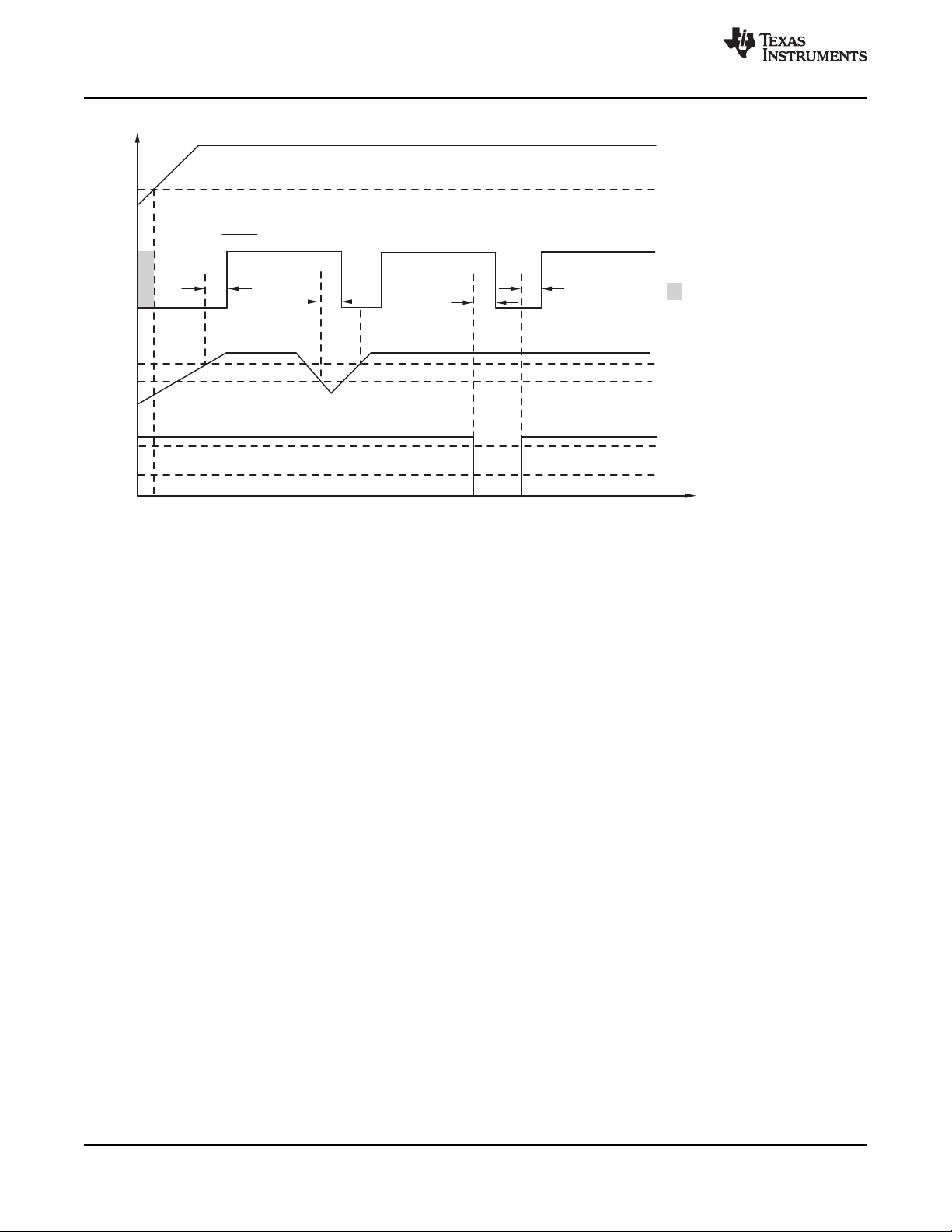
Time
0.8 V
V
ITP
V
ITN
0.7 V
DD
0.3 V
DD
MR
SENSE
RESET
V
DD
t
PD(r)
t
PD(f)
t
PD(r)
t
PD(r)
=SENSE Rising Propagation Delay
= Undefined State
t
d(MR)
=SENSE Falling Propagation Delay
t
PD(f)
TPS3890-Q1
SBVS303B –MARCH 2017–REVISED FEBRUARY 2018
www.ti.com
Figure 1. Timing Diagram
6
Submit Documentation Feedback Copyright © 2017–2018, Texas Instruments Incorporated
Product Folder Links: TPS3890-Q1
Temperature (qC)
CT Current (PA)
-50 -25 0 25 50 75 100 125
1
1.05
1.1
1.15
1.2
D005
1.5 V
5.5 V
Hysteresis (%)
Frequency (%)
0
3
6
9
12
15
0.47 0.51 0.55 0.59 0.63 0.67
V
ITN
Accuracy (%)
Frequency (%)
0
2
4
6
8
10
12
-0.25 -0.15 -0.05 0.05 0.15 0.25
V
ITP
Accuracy (%)
Frequency (%)
0
2
4
6
8
10
12
-0.25 -0.15 -0.05 0.05 0.15 0.25
Temperature (qC)
Accuracy (%)
-50 -25 0 25 50 75 100 125
-0.75
-0.5
-0.25
0
0.25
0.5
0.75
D001
Unit 1
Unit 2
Unit 3
Unit 4
Unit 5
Avg
Temperature (qC)
Accuracy (%)
-50 -25 0 25 50 75 100 125
-0.75
-0.5
-0.25
0
0.25
0.5
0.75
D002
Unit 1
Unit 2
Unit 3
Unit 4
Unit 5
Avg
TPS3890-Q1
www.ti.com
SBVS303B –MARCH 2017–REVISED FEBRUARY 2018
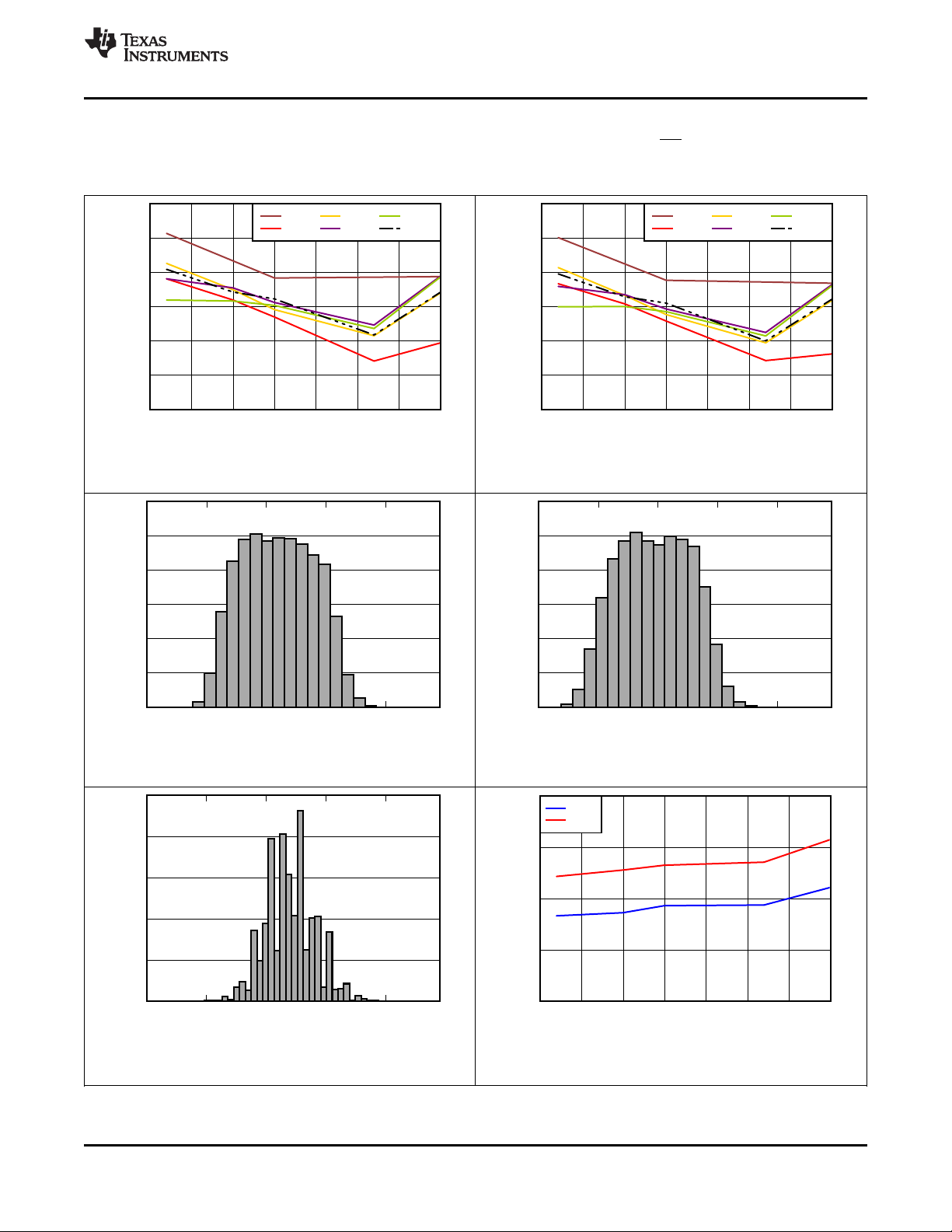
7.7 Typical Characteristics
over the operating junction temperature range of –40°C to +125°C, 1.5 V ≤ VDD≤ 5.5 V, and MR = VDD(unless otherwise
noted)
Figure 2. V
Accuracy vs Temperature Figure 3. V
ITN
Tested at VDD= 1.5 V and VDD= 5.5 V, total tests = 136,348
Figure 4. V
Accuracy Histogram
ITN
Accuracy vs Temperature
ITP
Tested at VDD= 1.5 V and VDD= 5.5 V, total tests = 136,348
Figure 5. V
Accuracy Histogram
ITP
Tested at VDD= 1.5 V and VDD= 5.5 V, total tests = 136,348
Figure 6. Hysteresis Histogram
Product Folder Links: TPS3890-Q1
Figure 7. CT Current vs Temperature
Submit Documentation FeedbackCopyright © 2017–2018, Texas Instruments Incorporated
7
Temperature (qC)
Startup Delay (Ps)
-50 -25 0 25 50 75 100 125
0
100
200
300
400
500
600
D008
VCC = 1.5 V
VCC = 3.3 V
VCC = 5.5 V
Overdrive (%)
Propagation Delay (Ps)
1 10 100
29
30
31
32
33
34
D009
-40qC
0qC
25qC
85qC
125qC
Temperature (qC)
MR Threshold (V)
-50 -25 0 25 50 75 100 125
0
0.25
0.5
0.75
1
D006
V
IL
V
IH
Temperature (qC)
MR Threshold (V)
-50 -25 0 25 50 75 100 125
1
1.25
1.5
1.75
2
2.25
2.5
2.75
3
V
IL
V
IH
VDD (V)
Supply Current (PA)
0 0.5 1 1.5 2 2.5 3 3.5 4 4.5 5 5.5
0
1
2
3
4
5
6
D004
-40qC
0qC
25qC
85qC
105qC
125qC
VDD (V)
Supply Current (PA)
0 0.5 1 1.5 2 2.5 3 3.5 4 4.5 5 5.5
0
1
2
3
4
5
6
-40qC
0qC
25qC
85qC
105qC
125q
TPS3890-Q1
SBVS303B –MARCH 2017–REVISED FEBRUARY 2018
www.ti.com
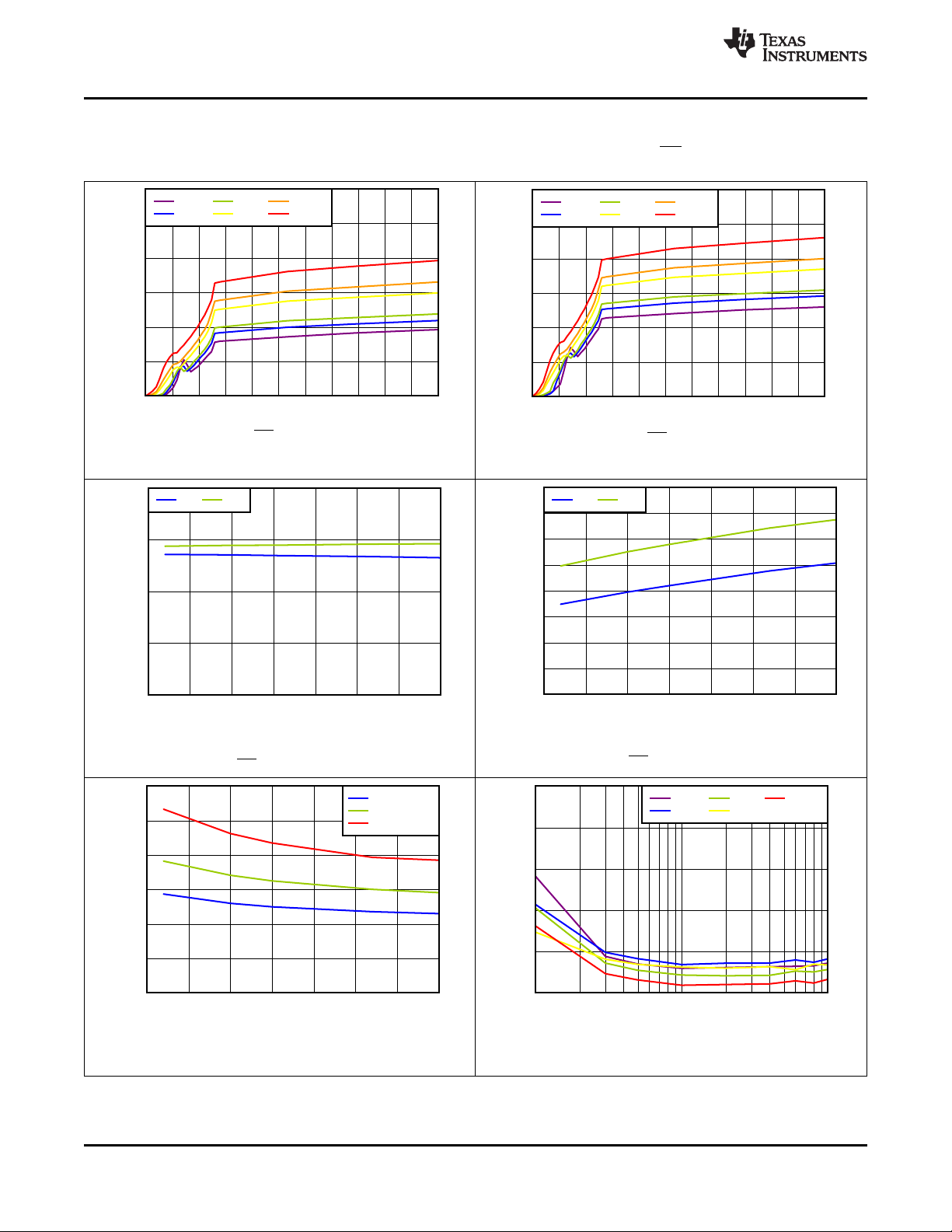
Typical Characteristics (continued)
over the operating junction temperature range of –40°C to +125°C, 1.5 V ≤ VDD≤ 5.5 V, and MR = VDD(unless otherwise
noted)
MR = V
DD
Figure 8. Supply Current vs Power-Supply Voltage
Figure 9. Supply Current vs Power-Supply Voltage
MR = 0 V
VDD= 1.5 V
Figure 10. MR Threshold vs Temperature
Figure 12. Startup Delay vs Temperature
8
Submit Documentation Feedback Copyright © 2017–2018, Texas Instruments Incorporated
Product Folder Links: TPS3890-Q1
VDD= 5.5 V
Figure 11. MR Threshold vs Temperature
VDD= 5.5 V
Figure 13. Propagation Delay (t
PD(r)
) vs Overdrive
Temperature (qC)
SENSE Glitch Immunity (Ps)
-50 -25 0 25 50 75 100 125
0
2
4
6
8
10
12
14
16
18
20
D017
Overdrive=3%
Overdrive=5%
Overdrive=10%
Temperature (qC)
SENSE Glitch Immunity (Ps)
-50 -25 0 25 50 75 100 125
29
29.5
30
30.5
31
31.5
32
Overdrive=3%
Overdrive=5%
Overdrive=10%
Overdrive (%)
Propagation Delay (Ps)
1 10 100
2
6
10
14
18
22
26
30
34
D012
-40qC
0qC
25qC
85qC
125qC
Temperature (qC)
SENSE Glitch Immunity (Ps)
-50 -25 0 25 50 75 100 125
29
29.5
30
30.5
31
31.5
32
Overdrive=3%
Overdrive=5%
Overdrive=10%
Overdrive (%)
Propagation Delay (Ps)
1 10 100
29
30
31
32
33
34
D010
-40qC
0qC
25qC
85qC
125qC
Overdrive (%)
Propagation Delay (Ps)
1 10 100
2
6
10
14
18
22
26
30
34
D011
-40qC
0qC
25qC
85qC
125qC
TPS3890-Q1
www.ti.com
SBVS303B –MARCH 2017–REVISED FEBRUARY 2018
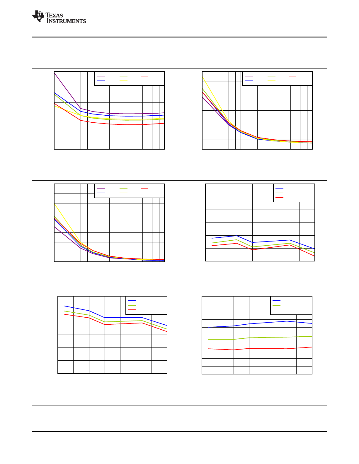
Typical Characteristics (continued)
over the operating junction temperature range of –40°C to +125°C, 1.5 V ≤ VDD≤ 5.5 V, and MR = VDD(unless otherwise
noted)
VDD= 1.5 V
Figure 14. Propagation Delay (t
VDD= 1.5 V
Figure 16. Propagation Delay (t
) vs Overdrive
PD(r)
) vs Overdrive
PD(f)
VDD= 5.5 V
Figure 15. Propagation Delay (t
) vs Overdrive
PD(f)
VDD= 5.5 V
Figure 17. Low-to-High Glitch Immunity vs Temperature
Figure 18. Low-to-High Glitch Immunity vs Temperature
VDD= 1.5 V
Figure 19. High-to-Low Glitch Immunity vs Temperature
Product Folder Links: TPS3890-Q1
VDD= 5.5 V
Submit Documentation FeedbackCopyright © 2017–2018, Texas Instruments Incorporated
9

I
RESET
(mA)
V
OL
(V)
0 1 2 3 4 5
0
0.2
0.4
0.6
0.8
1
1.2
1.4
1.6
-40qC
0qC
25qC
85qC
105qC
125qC
Temperature (qC)
SENSE Glitch Immunity (Ps)
-50 -25 0 25 50 75 100 125
0
2
4
6
8
10
12
14
16
18
20
D018
Overdrive=3%
Overdrive=5%
Overdrive=10%
I
RESET
(mA)
V
OL
(V)
0 1 2 3 4 5
0
0.2
0.4
0.6
0.8
1
1.2
1.4
1.6
D015
-40qC
0qC
25qC
85qC
105qC
125qC
TPS3890-Q1
SBVS303B –MARCH 2017–REVISED FEBRUARY 2018
www.ti.com
Typical Characteristics (continued)
over the operating junction temperature range of –40°C to +125°C, 1.5 V ≤ VDD≤ 5.5 V, and MR = VDD(unless otherwise
noted)
VDD= 1.5 V
Figure 20. High-to-Low Glitch Immunity vs Temperature
VDD= 1.5 V
Figure 22. Low-Level Output Voltage vs RESET Current
VDD= 5.5 V
Figure 21. Low-Level Output Voltage vs RESET Current
10
Submit Documentation Feedback Copyright © 2017–2018, Texas Instruments Incorporated
Product Folder Links: TPS3890-Q1

TPS389001-Q1
Adjustable Version
V
DD
MR
SENSE
RESET
CT
GND
1.15 V
V
REF
Reset
Logic
Timer
Fixed Voltage VersionAdjustable Voltage Version
V
DD
MR
SENSE
RESET
CT
GND
1.15 V
V
REF
Reset
Logic
Timer
R
2
R
1
Copyright © 2016,Texas Instruments Incorporated
TPS3890-Q1
www.ti.com
SBVS303B –MARCH 2017–REVISED FEBRUARY 2018
8 Detailed Description
8.1 Overview
The TPS3890-Q1 supervisory product family is designed to assert a RESET signal when either the SENSE pin
voltage drops below V
adjustable time after both the manual reset (MR) and SENSE voltages return above their respective thresholds.
8.2 Functional Block Diagram
or the manual reset (MR) is driven low. The RESET output remains asserted for a user-
ITN
8.3 Feature Description
The combination of user-adjustable reset delay time with a broad range of threshold voltages allow these devices
to be used in a wide array of applications. Fixed negative threshold voltages (V
to 3.17 V (see the Device Comparison Table for available options), and the adjustable device can be used to
customize the threshold voltage for other application needs by using an external resistor divider. The CT pin
allows the reset delay to be set between 25 μs and 30 s with the use of an external capacitor.
8.3.1 User-Configurable RESET Delay Time
The rising RESET delay time (t
) can be configured by installing a capacitor connected to the CT pin. The
PD(r)
TPS3890-Q1 uses a CT pin charging current (ICT) of 1.15 µA to help counter the effect of capacitor and boardlevel leakage currents that can be substantial in certain applications. The rising RESET delay time can be set to
any value between 25 µs (no CCTinstalled) and 30 s (CCT= 26 µF).
The capacitor value needed for a given delay time can be calculated using Equation 1:
t
(sec) = CCT× VCT÷ ICT+ t
PD(r)
The slope of Equation 1 is determined by the time that the CT charging current (ICT) takes to charge the external
capacitor up to the CT comparator threshold voltage (VCT). When RESET is asserted, the capacitor is discharged
PD(r)(nom)
through the internal CT pulldown resistor (RCT). When the RESET conditions are cleared, the internal precision
current source is enabled and begins to charge the external capacitor and when the voltage on this capacitor
reaches 1.22 V, RESET is deasserted. Note that in order to minimize the difference between the calculated
RESET delay time and the actual RESET delay time, use a low-leakage type capacitor (such as a ceramic
capacitor) and minimize parasitic board capacitance around this pin.
Product Folder Links: TPS3890-Q1
) can be factory set from 1.15 V
ITN
Submit Documentation FeedbackCopyright © 2017–2018, Texas Instruments Incorporated
(1)
11

1.2 V 3.3 V
TPS389033-Q1
SEN SE VDDVDD S ENS E
V
I/OVCORE
GP IO
GNDGNDGND
CTCT
TPS389012-Q1 DSP
3.3 V
Copyright © 2016, Texas Instruments Incorporated
RESET
MR
MR
RESET
TPS3890-Q1
SBVS303B –MARCH 2017–REVISED FEBRUARY 2018
www.ti.com
Feature Description (continued)
8.3.2 Manual Reset (MR) Input
The manual reset (MR) input allows a processor or other logic circuits to initiate a reset. A logic low on MR
causes RESET to assert. After MR returns to a logic high and SENSE is above V
the user-defined reset delay. If MR is not controlled externally, then MR must be connected to VDD. Note that if
the logic signal driving MR is not greater than or equal to VDD, then some additional current flows into VDD and
out of MR and the difference is apparent when comparing Figure 8 and Figure 9.
Figure 23 shows how MR can be used to monitor multiple system voltages when only a single CT capacitor is
needed to set the RESET delay time.
, RESET is deasserted after
ITP
8.3.3 RESET Output
RESET remains high (deasserted) as long as SENSE is above the positive threshold (V
signal (MR) is logic high. If SENSE falls below the negative threshold (V
asserted, driving the RESET pin to a low impedance.
When MR is again logic high and SENSE is above V
specified reset delay period (t
state and uses a pullup resistor to hold RESET high. Connect the pullup resistor to the proper voltage rail to
enable the outputs to be connected to other devices at the correct interface voltage level. RESET can be pulled
up to any voltage up to 5.5 V, independent of the device supply voltage. To ensure proper voltage levels, give
some consideration when choosing the pullup resistor values. The pullup resistor value is determined by VOL, the
output capacitive loading, and the output leakage current (I
8.3.4 SENSE Input
The SENSE input can vary from ground to 5.5 V (7.0 V, absolute maximum), regardless of the device supply
voltage used. The SENSE pin is used to monitor the critical voltage rail. If the voltage on this pin drops below
V
, then RESET is asserted. When the voltage on the SENSE pin exceeds the positive threshold voltage,
ITN
RESET deasserts after the user-defined RESET delay time.
The internal comparator has built-in hysteresis to ensure well-defined RESET assertions and deassertions even
when there are small changes on the voltage rail being monitored.
The TPS3890-Q1 device is relatively immune to short transients on the SENSE pin. Glitch immunity is dependent
on threshold overdrive, as illustrated in Figure 19 for V
cases, for noisy applications good analog design practice is to place a 1-nF to 10-nF bypass capacitor at the
SENSE input to reduce sensitivity to transient voltages on the monitored signal.
Figure 23. Using MR to Monitor Multiple System Voltages
) or if MR is driven low, then RESET is
ITN
, a delay circuit is enabled that holds RESET low for a
). When the reset delay has elapsed, the RESET pin goes to a high-impedance
PD(r)
ITP
).
LKG(OD)
and Figure 18 for V
ITN
. Although not required in most
ITP
) and the manual reset
ITP
12
Submit Documentation Feedback Copyright © 2017–2018, Texas Instruments Incorporated
Product Folder Links: TPS3890-Q1

V
MON
TPS389001-Q1
MR
SENSE
GND
RESET
R
1
R
2
V
IN
Copyright © 2016, Texas Instruments Incorporated
VDD
R
PU
TPS3890-Q1
www.ti.com
SBVS303B –MARCH 2017–REVISED FEBRUARY 2018
Feature Description (continued)
The adjustable version (TPS389001-Q1) can be used to monitor any voltage rail down to 1.15 V using the circuit
shown in Figure 24.
Figure 24. Using the TPS389001-Q1 to Monitor a User-Defined Threshold Voltage
The target threshold voltage for the monitored supply (V
ITx(MON)
) and the resistor divider values can be calculated
by using Equation 2 and Equation 3, respectively:
V
Equation 3 can be used to calculate either the negative threshold or the positive threshold by replacing V
either V
R
ITx(MON)
ITN
TOTAL
= V
ITx
or V
ITP
= R1+ R
× (1 + R1÷ R2) (2)
with
ITx
, respectively.
2
(3)
Resistors with high values minimize current consumption; however, the input bias current of the device degrades
accuracy if the current through the resistors is too low. Therefore, choosing an R
value so that the current
TOTAL
through the resistor divider is at least 100 times larger than the SENSE input current is simplest. See the
Optimizing Resistor Dividers at a Comparator Input application report for more details on sizing input resistors.
8.3.4.1 Immunity to SENSE Pin Voltage Transients
The TPS3890-Q1 is immune to short voltage transient spikes on the input pins. Sensitivity to transients depends
on both transient duration and overdrive (amplitude) of the transient. Overdrive is defined by how much VSENSE
exceeds the specified threshold, and is important to know because the smaller the overdrive, the slower the
response of the outputs (that is, undervoltage and overvoltage). Threshold overdrive is calculated as a percent of
the threshold in question, as shown in Equation 4.
Overdrive = | (V
SENSE
/ V
– 1) × 100% | (4)
ITx
Figure 17 to Figure 20 illustrate the glitch immunity that the TPS3890-Q1 has versus temperature with three
different overdrive voltages. The propagation delay versus overdrive curves (Figure 13 to Figure 16) can be used
to determine how sensitive the TPS3890-Q1 family of devices are across an even wider range of overdrive
voltages.
Product Folder Links: TPS3890-Q1
Submit Documentation FeedbackCopyright © 2017–2018, Texas Instruments Incorporated
13

TPS3890-Q1
SBVS303B –MARCH 2017–REVISED FEBRUARY 2018
8.4 Device Functional Modes
Table 1 summarizes the various functional modes of the device.
Table 1. Truth Table
V
DD
VDD< V
POR
V
< VDD< V
POR
VDD≥ V
VDD≥ V
VDD≥ V
(1) When VDDfalls below V
DD(MIN)
DD(MIN)
DD(MIN)
DD(MIN)
(1)
, undervoltage-lockout (UVLO) takes effect and RESET is held low until VDDfalls below V
DD(MIN)
MR SENSE RESET
— — Undefined
— — L
L — L
H V
H V
SENSE
SENSE
< V
> V
ITN
ITP
L
H
POR
www.ti.com
.
8.4.1 Normal Operation (VDD> V
When VDDis greater than V
DD(min)
, the RESET signal is determined by the voltage on the SENSE pin and the
DD(min)
)
logic state of MR.
• MR high: when the voltage on VDD is greater than 1.5 V, the RESET signal corresponds to the voltage on
the SENSE pin relative to the threshold voltage.
• MR low: in this mode, RESET is held low regardless of the voltage on the SENSE pin.
8.4.2 Above Power-On-Reset But Less Than V
When the voltage on VDD is less than the V
DD(min)
DD(min)(VPOR
voltage, and greater than the power-on-reset voltage (V
< VDD< V
DD(min)
)
POR
the RESET signal is asserted regardless of the voltage on the SENSE pin.
8.4.3 Below Power-On-Reset (VDD< V
When the voltage on VDD is lower thanV
)
POR
, the device does not have enough voltage to internally pull the
POR
asserted output low and RESET is undefined and must not be relied upon for proper device function.
),
14
Submit Documentation Feedback Copyright © 2017–2018, Texas Instruments Incorporated
Product Folder Links: TPS3890-Q1

1.8 V
TPS389018-Q1
VDD VDDSENSE
GNDGND
MR
CT
RESET
XRS
1 MW
Delfino MCU
TM
1.5 nF
Copyright © 2016, Texas Instruments Incorporated
3.3 V
External
Reset
TPS3890-Q1
www.ti.com
SBVS303B –MARCH 2017–REVISED FEBRUARY 2018
9 Application and Implementation
NOTE
Information in the following applications sections is not part of the TI component
specification, and TI does not warrant its accuracy or completeness. TI’s customers are
responsible for determining suitability of components for their purposes. Customers should
validate and test their design implementation to confirm system functionality.
9.1 Application Information
The following sections describe in detail how to properly use this device, depending on the requirements of the
final application.
9.2 Typical Application
A typical application for the TPS389018-Q1 is shown in Figure 25. The TPS389018-Q1 can be used to monitor
the 1.8-V VDD rail required by the TI Delfino™ microprocessor family. The open-drain RESET output of the
TPS389018-Q1 is connected to the XRS input of the microprocessor. A reset event is initiated when the VDD
voltage is less than V
or when MR is driven low by an external source.
ITN
Figure 25. TPS3890-Q1 Monitoring the Supply Voltage for a Delfino Microprocessor
9.2.1 Design Requirements
The TPS3890-Q1 RESET output can be used to drive the reset (XRS) input of a microprocessor. The RESET pin
of the TPS3890-Q1 is pulled high with a 1-MΩ resistor; the reset delay time is controlled by the CT capacitor and
is set depending on the reset requirement times of the microprocessor. During power-up, XRS must remain low
for at least 1 ms after VDD reaches 1.5 V for the C2000™ Delfino family of microprocessors. For 100-MHz
operation, the Delfino TMS320F2833x microcontroller uses a supply voltage of 1.8 V that must be monitored by
the TPS3890-Q1.
9.2.2 Detailed Design Procedure
The primary constraint for this application is choosing the correct device to monitor the supply voltage of the
microprocessor. The TPS389018-Q1 has a negative threshold of 1.73 V and a positive threshold of 1.74 V,
making the device suitable for monitoring a 1.8-V rail. The secondary constraint for this application is the reset
delay time that must be at least 1 ms to allow the Delfino microprocessor enough time to startup up correctly.
Because a minimum time is required, the worst-case scenario is a supervisor with a high CT charging current
(ICT) and a low CT comparator threshold (VCT). For applications with ambient temperatures ranging from –40°C
to +125°C, CCTcan be calculated using I
CT(Max)
, V
, and solving for CCTin Equation 1 such that the
CT(MIN)
minimum capacitance required at the CT pin is 1.149 nF. If standard capacitors with ±20% tolerances are used,
then the CT capacitor must be 1.5 nF or larger to ensure that the 1-ms delay time is met.
A 0.1-µF decoupling capacitor is connected to the VDD pin as a good analog design practice and a 1-MΩ
resistor is used as the RESET pullup resistor to minimize the current consumption when RESET is asserted. The
MR pin can be connected to an external signal if desired or connected to VDD if not used.
Product Folder Links: TPS3890-Q1
Submit Documentation FeedbackCopyright © 2017–2018, Texas Instruments Incorporated
15

Temperature (qC)
Startup Delay (Ps)
-50 -25 0 25 50 75 100 125
0
100
200
300
400
500
600
D008
VCC = 1.5 V
VCC = 3.3 V
VCC = 5.5 V
TPS3890-Q1
SBVS303B –MARCH 2017–REVISED FEBRUARY 2018
Typical Application (continued)
9.2.3 Application Curve
Figure 26. Startup Delay vs Temperature
10 Power Supply Recommendations
www.ti.com
These devices are designed to operate from an input supply with a voltage range between 1.5 V and 5.5 V. An
input supply capacitor is not required for this device; however, if the input supply is noisy, then good analog
practice is to place a 0.1-µF capacitor between the VDD pin and the GND pin. This device has a 7-V absolute
maximum rating on the VDD pin. If the voltage supply providing power to VDD is susceptible to any large voltage
transient that can exceed 7 V, additional precautions must be taken.
16
Submit Documentation Feedback Copyright © 2017–2018, Texas Instruments Incorporated
Product Folder Links: TPS3890-Q1

GND
C
IN
MR
GND
RESET
VDD
SENSE
CT
Vias used to connect pins for application-specific connections
C
CT
R
PU
TPS3890-Q1
www.ti.com
SBVS303B –MARCH 2017–REVISED FEBRUARY 2018
11 Layout
11.1 Layout Guidelines
Make sure that the connection to the VDD pin is low impedance. Good analog design practice is to place a
0.1-µF ceramic capacitor near the VDD pin. If a capacitor is not connected to the CT pin, then minimize parasitic
capacitance on this pin so the RESET delay time is not adversely affected.
11.2 Layout Example
The layout example in shows how the TPS3890-Q1 is laid out on a printed circuit board (PCB) with a userdefined delay.
Figure 27. Recommended Layout
Product Folder Links: TPS3890-Q1
Submit Documentation FeedbackCopyright © 2017–2018, Texas Instruments Incorporated
17

TPS3890-Q1
SBVS303B –MARCH 2017–REVISED FEBRUARY 2018
www.ti.com
12 Device and Documentation Support
12.1 Device Support
12.1.1 Device Nomenclature
Table 2 shows how to decode the function of the device based on the part number, with TPS389033G-Q1 used
as an example.
Table 2. Device Naming Convention
DESCRIPTION NOMENCLATURE VALUE
(high-accuracy supervisor family)
TPS3890
33
(nominal rail voltage to be monitored)
G
(percent below nominal rail voltage for V
Q1
(automotive version)
ITN
)
— —
10 1.0 V
12 1.2 V
18 1.8 V
33 3.3 V
50 5.0 V
— 4%
G 7%
K 11%
L 12%
— —
12.2 Documentation Support
12.2.1 Related Documentation
For related documentation see the following:
• Optimizing Resistor Dividers at a Comparator Input
• Sensitivity Analysis for Power Supply Design
• Getting Started With TMS320C28x Digital Signal Controllers
• TPS3890EVM-775 Evaluation Module User Guide
• C2000 Delfino Family of Microprocessors
• TMS320F2833x Digital Signal Controllers (DSCs)
12.3 Receiving Notification of Documentation Updates
To receive notification of documentation updates, navigate to the device product folder on ti.com. In the upper
right corner, click on Alert me to register and receive a weekly digest of any product information that has
changed. For change details, review the revision history included in any revised document.
12.4 Community Resources
The following links connect to TI community resources. Linked contents are provided "AS IS" by the respective
contributors. They do not constitute TI specifications and do not necessarily reflect TI's views; see TI's Terms of
Use.
TI E2E™ Online Community TI's Engineer-to-Engineer (E2E) Community. Created to foster collaboration
among engineers. At e2e.ti.com, you can ask questions, share knowledge, explore ideas and help
solve problems with fellow engineers.
Design Support TI's Design Support Quickly find helpful E2E forums along with design support tools and
contact information for technical support.
18
Submit Documentation Feedback Copyright © 2017–2018, Texas Instruments Incorporated
Product Folder Links: TPS3890-Q1

TPS3890-Q1
www.ti.com
SBVS303B –MARCH 2017–REVISED FEBRUARY 2018
12.5 Trademarks
Delfino, C2000, E2E are trademarks of Texas Instruments.
All other trademarks are the property of their respective owners.
12.6 Electrostatic Discharge Caution
This integrated circuit can be damaged by ESD. Texas Instruments recommends that all integrated circuits be handled with
appropriate precautions. Failure to observe proper handling and installation procedures can cause damage.
ESD damage can range from subtle performance degradation to complete device failure. Precision integrated circuits may be more
susceptible to damage because very small parametric changes could cause the device not to meet its published specifications.
12.7 Glossary
SLYZ022 — TI Glossary.
This glossary lists and explains terms, acronyms, and definitions.
13 Mechanical, Packaging, and Orderable Information
The following pages include mechanical, packaging, and orderable information. This information is the most
current data available for the designated devices. This data is subject to change without notice and revision of
this document. For browser-based versions of this data sheet, refer to the left-hand navigation.
Product Folder Links: TPS3890-Q1
Submit Documentation FeedbackCopyright © 2017–2018, Texas Instruments Incorporated
19

PACKAGE OPTION ADDENDUM
www.ti.com
PACKAGING INFORMATION
Orderable Device Status
TPS389001QDSERQ1 ACTIVE WSON DSE 6 3000 RoHS & Green NIPDAUAG Level-1-260C-UNLIM -40 to 125 2N
TPS389012QDSERQ1 ACTIVE WSON DSE 6 3000 RoHS & Green NIPDAUAG Level-1-260C-UNLIM -40 to 125 2O
TPS389015QDSERQ1 ACTIVE WSON DSE 6 3000 RoHS & Green NIPDAUAG Level-1-260C-UNLIM -40 to 125 2P
TPS389018QDSERQ1 ACTIVE WSON DSE 6 3000 RoHS & Green NIPDAUAG Level-1-260C-UNLIM -40 to 125 2Q
TPS389025QDSERQ1 ACTIVE WSON DSE 6 3000 RoHS & Green NIPDAUAG Level-1-260C-UNLIM -40 to 125 2R
TPS389030QDSERQ1 ACTIVE WSON DSE 6 3000 RoHS & Green NIPDAUAG Level-1-260C-UNLIM -40 to 125 2S
TPS389033GQDSERQ1 ACTIVE WSON DSE 6 3000 RoHS & Green NIPDAUAG Level-1-260C-UNLIM -40 to 125 7V
TPS389033KQDSERQ1 ACTIVE WSON DSE 6 3000 RoHS & Green NIPDAUAG Level-1-260C-UNLIM -40 to 125 7W
TPS389033QDSERQ1 ACTIVE WSON DSE 6 3000 RoHS & Green NIPDAUAG Level-1-260C-UNLIM -40 to 125 2T
TPS389050GQDSERQ1 ACTIVE WSON DSE 6 3000 RoHS & Green NIPDAUAG Level-1-260C-UNLIM -40 to 125 7T
TPS389050LQDSERQ1 ACTIVE WSON DSE 6 3000 RoHS & Green NIPDAUAG Level-1-260C-UNLIM -40 to 125 7U
Package Type Package
(1)
Drawing
Pins Package
Qty
Eco Plan
(2)
Lead finish/
Ball material
(6)
MSL Peak Temp
(3)
Op Temp (°C) Device Marking
10-Dec-2020
Samples
(4/5)
TPS389050QDSERQ1 ACTIVE WSON DSE 6 3000 RoHS & Green NIPDAUAG Level-1-260C-UNLIM -40 to 125 7S
(1)
The marketing status values are defined as follows:
ACTIVE: Product device recommended for new designs.
LIFEBUY: TI has announced that the device will be discontinued, and a lifetime-buy period is in effect.
NRND: Not recommended for new designs. Device is in production to support existing customers, but TI does not recommend using this part in a new design.
PREVIEW: Device has been announced but is not in production. Samples may or may not be available.
OBSOLETE: TI has discontinued the production of the device.
(2)
RoHS: TI defines "RoHS" to mean semiconductor products that are compliant with the current EU RoHS requirements for all 10 RoHS substances, including the requirement that RoHS substance
do not exceed 0.1% by weight in homogeneous materials. Where designed to be soldered at high temperatures, "RoHS" products are suitable for use in specified lead-free processes. TI may
reference these types of products as "Pb-Free".
RoHS Exempt: TI defines "RoHS Exempt" to mean products that contain lead but are compliant with EU RoHS pursuant to a specific EU RoHS exemption.
Green: TI defines "Green" to mean the content of Chlorine (Cl) and Bromine (Br) based flame retardants meet JS709B low halogen requirements of <=1000ppm threshold. Antimony trioxide based
flame retardants must also meet the <=1000ppm threshold requirement.
Addendum-Page 1

PACKAGE OPTION ADDENDUM
www.ti.com
(3)
MSL, Peak Temp. - The Moisture Sensitivity Level rating according to the JEDEC industry standard classifications, and peak solder temperature.
10-Dec-2020
(4)
There may be additional marking, which relates to the logo, the lot trace code information, or the environmental category on the device.
(5)
Multiple Device Markings will be inside parentheses. Only one Device Marking contained in parentheses and separated by a "~" will appear on a device. If a line is indented then it is a continuation
of the previous line and the two combined represent the entire Device Marking for that device.
(6)
Lead finish/Ball material - Orderable Devices may have multiple material finish options. Finish options are separated by a vertical ruled line. Lead finish/Ball material values may wrap to two
lines if the finish value exceeds the maximum column width.
Important Information and Disclaimer:The information provided on this page represents TI's knowledge and belief as of the date that it is provided. TI bases its knowledge and belief on information
provided by third parties, and makes no representation or warranty as to the accuracy of such information. Efforts are underway to better integrate information from third parties. TI has taken and
continues to take reasonable steps to provide representative and accurate information but may not have conducted destructive testing or chemical analysis on incoming materials and chemicals.
TI and TI suppliers consider certain information to be proprietary, and thus CAS numbers and other limited information may not be available for release.
In no event shall TI's liability arising out of such information exceed the total purchase price of the TI part(s) at issue in this document sold by TI to Customer on an annual basis.
OTHER QUALIFIED VERSIONS OF TPS3890-Q1 :
Catalog: TPS3890
•
NOTE: Qualified Version Definitions:
Catalog - TI's standard catalog product
•
Addendum-Page 2

PACKAGE MATERIALS INFORMATION
www.ti.com 9-Mar-2018
TAPE AND REEL INFORMATION
*All dimensions are nominal
Device Package
Type
TPS389001QDSERQ1 WSON DSE 6 3000 180.0 8.4 1.83 1.83 0.89 4.0 8.0 Q2
TPS389012QDSERQ1 WSON DSE 6 3000 180.0 8.4 1.83 1.83 0.89 4.0 8.0 Q2
TPS389015QDSERQ1 WSON DSE 6 3000 180.0 8.4 1.83 1.83 0.89 4.0 8.0 Q2
TPS389018QDSERQ1 WSON DSE 6 3000 180.0 8.4 1.83 1.83 0.89 4.0 8.0 Q2
TPS389025QDSERQ1 WSON DSE 6 3000 180.0 8.4 1.83 1.83 0.89 4.0 8.0 Q2
TPS389030QDSERQ1 WSON DSE 6 3000 180.0 8.4 1.83 1.83 0.89 4.0 8.0 Q2
TPS389033GQDSERQ1 WSON DSE 6 3000 180.0 8.4 1.83 1.83 0.89 4.0 8.0 Q2
TPS389033KQDSERQ1 WSON DSE 6 3000 180.0 8.4 1.83 1.83 0.89 4.0 8.0 Q2
TPS389033QDSERQ1 WSON DSE 6 3000 180.0 8.4 1.83 1.83 0.89 4.0 8.0 Q2
TPS389050GQDSERQ1 WSON DSE 6 3000 180.0 8.4 1.83 1.83 0.89 4.0 8.0 Q2
TPS389050LQDSERQ1 WSON DSE 6 3000 180.0 8.4 1.83 1.83 0.89 4.0 8.0 Q2
TPS389050QDSERQ1 WSON DSE 6 3000 180.0 8.4 1.83 1.83 0.89 4.0 8.0 Q2
Package
Drawing
Pins SPQ Reel
Diameter
(mm)
Reel
Width
W1 (mm)
A0
(mm)B0(mm)K0(mm)P1(mm)W(mm)
Quadrant
Pin1
Pack Materials-Page 1

PACKAGE MATERIALS INFORMATION
www.ti.com 9-Mar-2018
*All dimensions are nominal
Device Package Type Package Drawing Pins SPQ Length (mm) Width (mm) Height (mm)
TPS389001QDSERQ1 WSON DSE 6 3000 183.0 183.0 20.0
TPS389012QDSERQ1 WSON DSE 6 3000 183.0 183.0 20.0
TPS389015QDSERQ1 WSON DSE 6 3000 183.0 183.0 20.0
TPS389018QDSERQ1 WSON DSE 6 3000 183.0 183.0 20.0
TPS389025QDSERQ1 WSON DSE 6 3000 183.0 183.0 20.0
TPS389030QDSERQ1 WSON DSE 6 3000 183.0 183.0 20.0
TPS389033GQDSERQ1 WSON DSE 6 3000 183.0 183.0 20.0
TPS389033KQDSERQ1 WSON DSE 6 3000 183.0 183.0 20.0
TPS389033QDSERQ1 WSON DSE 6 3000 183.0 183.0 20.0
TPS389050GQDSERQ1 WSON DSE 6 3000 183.0 183.0 20.0
TPS389050LQDSERQ1 WSON DSE 6 3000 183.0 183.0 20.0
TPS389050QDSERQ1 WSON DSE 6 3000 183.0 183.0 20.0
Pack Materials-Page 2


PACKAGE OUTLINE
PIN 1 INDEX AREA
0.8 MAX
SCALE 6.000
B
1.55
1.45
A
1.55
1.45
C
WSON - 0.8 mm max heightDSE0006A
PLASTIC SMALL OUTLINE - NO LEAD
SEATING PLANE
0.08 C
(0.2) TYP
0.05
0.00
4220552/A 04/2021
2X 1
5X
4X 0.5
0.6
0.4
3
1
0.7
0.5
PIN 1 ID
4
6
0.3
6X
0.2
0.1 C A B
0.05
C
NOTES:
1. All linear dimensions are in millimeters. Any dimensions in parenthesis are for reference only. Dimensioning and tolerancing
per ASME Y14.5M.
2. This drawing is subject to change without notice.
www.ti.com

EXAMPLE BOARD LAYOUT
WSON - 0.8 mm max heightDSE0006A
PLASTIC SMALL OUTLINE - NO LEAD
6X (0.25)
4X 0.5
(R0.05) TYP
(0.8)
1
3
PKG
(1.6)
5X (0.7)
6
SYMM
4
LAND PATTERN EXAMPLE
SCALE:40X
0.05 MAX
ALL AROUND
0.05 MIN
ALL AROUND
SOLDER MASK
OPENING
NON SOLDER MASK
METAL
PADS 4-6
DEFINED
METAL UNDER
SOLDER MASK
SOLDER MASK
SOLDER MASK DETAILS
NOTES: (continued)
3. For more information, see Texas Instruments literature number SLUA271 (www.ti.com/lit/slua271).
www.ti.com
SOLDER MASK
OPENING
PADS 1-3
DEFINED
4220552/A 04/2021

EXAMPLE STENCIL DESIGN
WSON - 0.8 mm max heightDSE0006A
PLASTIC SMALL OUTLINE - NO LEAD
6X (0.25)
4X (0.5)
(R0.05) TYP
PKG
(0.8)
1
3
(1.6)
5X (0.7)
6
SYMM
4
SOLDER PASTE EXAMPLE
BASED ON 0.125 mm THICK STENCIL
SCALE:40X
NOTES: (continued)
4. Laser cutting apertures with trapezoidal walls and rounded corners may offer better paste release. IPC-7525 may have alternate
design recommendations.
www.ti.com

IMPORTANT NOTICE AND DISCLAIMER
TI PROVIDES TECHNICAL AND RELIABILITY DATA (INCLUDING DATASHEETS), DESIGN RESOURCES (INCLUDING REFERENCE
DESIGNS), APPLICATION OR OTHER DESIGN ADVICE, WEB TOOLS, SAFETY INFORMATION, AND OTHER RESOURCES “AS IS”
AND WITH ALL FAULTS, AND DISCLAIMS ALL WARRANTIES, EXPRESS AND IMPLIED, INCLUDING WITHOUT LIMITATION ANY
IMPLIED WARRANTIES OF MERCHANTABILITY, FITNESS FOR A PARTICULAR PURPOSE OR NON-INFRINGEMENT OF THIRD
PARTY INTELLECTUAL PROPERTY RIGHTS.
These resources are intended for skilled developers designing with TI products. You are solely responsible for (1) selecting the appropriate
TI products for your application, (2) designing, validating and testing your application, and (3) ensuring your application meets applicable
standards, and any other safety, security, or other requirements. These resources are subject to change without notice. TI grants you
permission to use these resources only for development of an application that uses the TI products described in the resource. Other
reproduction and display of these resources is prohibited. No license is granted to any other TI intellectual property right or to any third party
intellectual property right. TI disclaims responsibility for, and you will fully indemnify TI and its representatives against, any claims, damages,
costs, losses, and liabilities arising out of your use of these resources.
TI’s products are provided subject to TI’s Terms of Sale (https:www.ti.com/legal/termsofsale.html) or other applicable terms available either
on ti.com or provided in conjunction with such TI products. TI’s provision of these resources does not expand or otherwise alter TI’s
applicable warranties or warranty disclaimers for TI products.IMPORTANT NOTICE
Mailing Address: Texas Instruments, Post Office Box 655303, Dallas, Texas 75265
Copyright © 2021, Texas Instruments Incorporated
 Loading...