

V
IT+(OV)
Accuracy (%)
Frequency (%)
-0.4 -0.3 -0.2 -0.1 0 0.1 0.2 0.3 0.4
0
5
10
15
20
25
30
35
D004
RESET
VDD
SENSE
MR
CT
GND
RESET
V
CORE
Processor
OV Threshold
Optional
Up to
5.5V
TPS3870Q1
1
Monitor Voltage
10k
2
3
4
5
6
Product
Folder
Order
Now
Technical
Documents
Tools &
Software
Support &
Community
TPS3870-Q1
SNVSBI5A –JULY 2019–REVISED SEPTEMBER 2019
TPS3870-Q1 Overvoltage Reset IC With Time Delay and Manual Reset
1 Features
1
• Qualified for automotive applications
• AEC-Q100 qualified with the following results:
– Device temperature grade 1: –40°C to +125°C
ambient operating temperature
– Device HBM ESD classification level 2
– Device CDM ESD classification level C7B
• Input voltage range: 1.7 V to 5.5 V
• Undervoltage lockout (UVLO): 1.7 V
• Low quiescent current: 7 µA (Max)
• High threshold accuracy:
– ± 0.25% (typical)
– ± 0.7% (–40°C to +125°C)
• Fixed threshold levels
– 50-mV steps from 500 mV to 1.3 V
– 1.5 V, 1.8 V, 2.5 V, 2.8 V, 2.9 V 3.3 V, 5 V
• User adjustable voltage threshold levels
• Internal glitch immunity and hysteresis
• Tolerance available from 3% to 7% in 1% steps
• Fixed time delay options: 50 µs, 1 ms, 5 ms, 10
ms, 20 ms, 100 ms, 200 ms
• Programmable time delay option with a single
external capacitor
• Open-drain active low OV monitor
• RESET voltage latching output mode
2 Applications
• Advanced driver assistance system (ADAS)
• Camera
• Sensor fusion
• HEV/EV
• FPGA, ASIC and DSP based systems
Integrated Overvoltage Detection
3 Description
The TPS3870-Q1 device is an integrated overvoltage
(OV) monitor or reset IC in industry’s smallest 6-pin
DSE package. This highly accurate voltage
supervisor is ideal for systems that operate on lowvoltage supply rails and have narrow margin supply
tolerances. Low threshold hysteresis prevent false
reset signals when the monitored voltage supply is in
its normal range of operation. Internal glitch immunity
and noise filters further eliminate false resets
resulting from erroneous signals.
The TPS3870-Q1 does not require any external
resistors for setting overvoltage reset thresholds,
which further optimizes overall accuracy, cost,
solution size, and improves reliability for safety
systems. The Capacitor Time (CT) pin is used to
select between the two available reset time delays
designed into each device and also to adjust the
reset time delay by connecting a capacitor. A
separate SENSE input pin and VDD pin allow for the
redundancy sought by high-reliability systems.
This device has a low typical quiescent current
specification of 4.5 µA (typical). The TPS3870-Q1 is
suitable for automotive applications and is qualified
for AEC-Q100 Grade 1.
Device Information
PART NUMBER PACKAGE BODY SIZE (NOM)
TPS3870-Q1 WSON (6) 1.50 mm × 1.50 mm
(1) For all available packages, see the orderable addendum at
the end of the data sheet.
Typical Overvoltage Accuracy Distribution
(1)
1
An IMPORTANT NOTICE at the end of this data sheet addresses availability, warranty, changes, use in safety-critical applications,
intellectual property matters and other important disclaimers. PRODUCTION DATA.

TPS3870-Q1
SNVSBI5A –JULY 2019–REVISED SEPTEMBER 2019
www.ti.com
Table of Contents
1 Features.................................................................. 1
2 Applications ........................................................... 1
3 Description............................................................. 1
4 Revision History..................................................... 2
5 Device Comparison Table..................................... 3
6 Pin Configuration and Functions......................... 4
7 Specifications......................................................... 5
7.1 Absolute Maximum Ratings ...................................... 5
7.2 ESD ratings............................................................... 5
7.3 Recommended Operating Conditions....................... 5
7.4 Thermal Information.................................................. 6
7.5 Electrical Characteristics........................................... 6
7.6 Timing Requirements................................................ 6
7.7 Typical Characteristics.............................................. 9
8 Detailed Description............................................ 12
8.1 Overview ................................................................. 12
8.2 Functional Block Diagram....................................... 12
8.3 Feature Description................................................. 12
8.4 Device Functional Modes........................................ 14
9 Application and Implementation ........................ 15
9.1 Application Information............................................ 15
9.2 Typical Application ................................................. 20
10 Power Supply Recommendations ..................... 22
10.1 Power Supply Guidelines...................................... 22
11 Layout................................................................... 22
11.1 Layout Guidelines ................................................. 22
11.2 Layout Example .................................................... 22
12 Device and Documentation Support................. 23
12.1 Device Nomenclature............................................ 23
12.2 Documentation Support ........................................ 24
12.3 Receiving Notification of Documentation Updates 24
12.4 Support Resources ............................................... 24
12.5 Trademarks........................................................... 24
12.6 Electrostatic Discharge Caution............................ 24
12.7 Glossary................................................................ 24
13 Mechanical, Packaging, and Orderable
Information........................................................... 24
4 Revision History
NOTE: Page numbers for previous revisions may differ from page numbers in the current version.
Changes from Original (July 2019) to Revision A Page
• Advance Information to Production Data release................................................................................................................... 1
2
Submit Documentation Feedback Copyright © 2019, Texas Instruments Incorporated
Product Folder Links: TPS3870-Q1
TPS3870-Q1
www.ti.com
SNVSBI5A –JULY 2019–REVISED SEPTEMBER 2019
5 Device Comparison Table
Table 1 shows the released versions of the TPS3870-Q1, including the nominal overvoltage thresholds. For all
possible voltages, threshold tolerance, time delays, and threshold options, see Table 6. Contact TI sales
representatives or on TI's E2E forum for details and availability of other options; minimum order quantities apply.
Table 1. Device Comparison Table
TIME DELAY (ms)
PART NUMBER V
TPS3870J4080DSERQ1 0.80 V Programmable 10 ms 200 ms 4%
TPS3870J4330DSERQ1 3.30 V Programmable 10 ms 200 ms 4%
MON
CT Pin =
Capacitor
CT Pin =
Open
CT Pin = VDD
THRESHOLD
TOLERANCE
Product Folder Links: TPS3870-Q1
Submit Documentation FeedbackCopyright © 2019, Texas Instruments Incorporated
3
SENSE
VDD
CT RESET
MR
GND
TPS3870-Q1
SNVSBI5A –JULY 2019–REVISED SEPTEMBER 2019
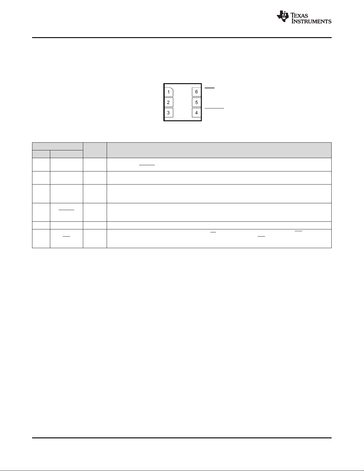
6 Pin Configuration and Functions
PIN
NO. NAME
1 SENSE I
2 VDD I
3 CT I
4 RESET O
5 GND — Ground
6 MR I
I/O DESCRIPTION
Input for the monitored supply voltage rail. When the SENSE voltage goes above the overvoltage
threshold, the RESET pin is driven low. Connect to VDD pin if monitoring VDD supply voltage.
Supply voltage input pin. Good analog design practice is to place a 0.1-μF ceramic capacitor close to
this pin.
Capacitor time delay pin. The CT pin offers two fixed time delays by connecting CT pin to VDD or
leaving it floating. Delay time can be programmed by connecting an external capacitor reference to
ground.
Active-low, open-drain output. This pin goes low when the SENSE voltage rises above the internally
overvoltage threshold (V
pull-up resistor terminated to the desired pull-up voltage.
Manual reset (MR), pull this pin to a logic low (V
deasserted the output goes high after the reset delay time(tD) expires. MR can be left floating when not
in use.
www.ti.com
DSE Package
6-Pin WSON
Top View
Pin Functions
). See the timing diagram in Figure 19 for more details. Connect this pin to a
IT+
) to assert a reset signal . After the MR pin is
MR_L
4
Submit Documentation Feedback Copyright © 2019, Texas Instruments Incorporated
Product Folder Links: TPS3870-Q1
TPS3870-Q1
www.ti.com
SNVSBI5A –JULY 2019–REVISED SEPTEMBER 2019
7 Specifications
7.1 Absolute Maximum Ratings
over operating free-air temperature range (unless otherwise noted)
Voltage V
Voltage V
Voltage V
Voltage V
Voltage V
Current I
Temperature
(2)
(1) Stresses beyond values listed under Absolute Maximum Ratings may cause permanent damage to the device. These are stress ratings
only, which do not imply functional operation of the device at these or any other conditions beyond those indicated under Recommended
Operating Conditions. Exposure to absolute-maximum-rated conditions for extended periods may affect device reliability.
(2) As a result of the low dissipated power in this device, it is assumed that TJ= TA.
DD
RESET
CT
SENSE
MR
RESET
Continuous total power dissipation See the Thermal Information
Operating junction temperature, T
Operating free-air temperature, T
Storage temperature, T
stg
7.2 ESD ratings
V
(ESD)
Electrostatic
discharge
(1) AEC Q100-002 indicates that HBM stressing shall be in accordance with the ANSI/ESDA/JEDEC JS-001 specification
Human-body model (HBM), per ANSI/ESDA/JEDEC JS-001
Charged-device model (CDM), per AEC
Q100-011
(1)
MIN MAX UNIT
–0.3 6 V
–0.3 6 V
–0.3 6 V
–0.3 6 V
–0.3 6 V
±40 mA
J
A
-40 150 °C
-40 150 °C
-65 150 °C
VALUE UNIT
(1)
All pins ±500
±2000
V
Corner pins ±750
7.3 Recommended Operating Conditions
V
DD
V
SENSE
V
CT
V
RESET
V
MR
I
RESET
T
J
(1) CT pin connected to VDD pin requires a pullup resistor; 10 kΩ is recommended.
(2) The maximum rating is VDDor 5.5 V, whichever is smaller.
(3) If the logic signal driving MR is less than VDD, then additional current flows into VDDand out of MR.
Supply pin voltage 1.7 5.5 V
Input pin voltage 0 5.5 V
CT pin voltage
(1) (2)
Output pin voltage 0 5.5 V
MR pin Voltage
(3)
Output pin current 0.3 10 mA
Junction temperature (free-air temperature) -40 125 ℃
MIN NOM MAX UNIT
V
DD
V
0 5.5 V
Product Folder Links: TPS3870-Q1
Submit Documentation FeedbackCopyright © 2019, Texas Instruments Incorporated
5
TPS3870-Q1
SNVSBI5A –JULY 2019–REVISED SEPTEMBER 2019
www.ti.com
7.4 Thermal Information
TPS3870-Q1
THERMAL METRIC
(1)
UNITDSE (WSON)
PINS
R
θJA
R
θJC(top)
R
θJB
Ψ
JT
Ψ
JB
R
θJC(bot)
Junction-to-ambient thermal resistance 184.2 °C/W
Junction-to-case (top) thermal resistance 30.6 °C/W
Junction-to-board thermal resistance 86.4 °C/W
Junction-to-top characterization parameter 13.4 °C/W
Junction-to-board characterization parameter 86.1 °C/W
Junction-to-case (bottom) thermal resistance N/A °C/W
(1) For more information about traditional and new thermal metrics, see the Semiconductor and IC Package Thermal Metrics application
report.
7.5 Electrical Characteristics
At 1.7 V ≤ VDD≤ 5.5 V, CT = MR = Open, RESET Voltage (V
operating free-air temperature range of – 40°C to 125°C, unless otherwise noted. Typical values are at TJ= 25°C, typical
conditions at VDD= 3.3 V.
PARAMETER TEST CONDITIONS MIN TYP MAX UNIT
V
DD
UVLO Under Voltage Lockout
V
POR
V
IT+(OV)
V
HYS
I
DD
I
SENSE
V
OL
I
LKG
V
MR_L
V
MR_H
V
CT_H
R
MR
I
CT
V
CT
(1) RESET pin is driven low when VDDfalls below UVLO.
(2) V
POR
(3) Hysteresis is with respect of the trip point (V
(4) VCTvoltage refers to the comparator threshold voltage that measures the voltage level of the external capacitor at CT pin.
Supply Voltage 1.7 5.5 V
Power on reset voltage
(1)
(2)
VDDfalling below 1.7 V 1.2 1.7 V
VOL(max) = 0.25 V, I
Positive- going threshold accuracy -0.7 ±0.25 0.7 %
Hysteresis Voltage
(3)
Supply current VDD≤ 5.5 V 4.5 7 µA
Input current, SENSE pin V
= 5 V 1 1.5 µA
SENSE
VDD= 1.7 V, I
Low level output voltage
VDD= 2 V, I
VDD= 5 V, I
Open drain output leakage current VDD= V
RESET
MR logic low input 0.3 V
MR logic high input 1.4 V
High level CT pin voltage 1.4 V
Manual reset Internal pullup resistance 100 KΩ
CT pin charge current 337 375 413 nA
CT pin comparator threshold voltage
(4)
is the minimum VDDvoltage level for a controlled output state.
)
IT+(OV)
) = 10 kΩ to VDD, RESET load = 10 pF, and over the
RESET
= 15 µA 1 V
OUT
0.3 0.55 0.8 %
= 0.4 mA 250 mV
OUT
= 3 mA 250 mV
OUT
= 5 mA 250 mV
OUT
= 5.5 V 300 nA
1.133 1.15 1.167 V
7.6 Timing Requirements
At 1.7 V ≤ VDD≤ 5.5 V, CT = MR = Open, RESET Voltage (V
operating free-air temperature range of – 40°C to 125°C, unless otherwise noted. Typical values are at TJ= 25°C, typical
conditions at VDD= 3.3 V.
t
D
t
D
t
D
t
D
t
D
t
D
6
Reset time delay, TPS3870J CT = Open 7 10 13 ms
Reset time delay, TPS3870J CT = 10 kΩ to V
Reset time delay, TPS3870K CT = Open 0.7 1 1.3 ms
Reset time delay, TPS3870K CT = 10 kΩ to V
Reset time delay, TPS3870L CT = Open 3.5 5 6.5 ms
Reset time delay, TPS3870L CT = 10 kΩ to V
Submit Documentation Feedback Copyright © 2019, Texas Instruments Incorporated
Product Folder Links: TPS3870-Q1
) = 10 kΩ to VDD, RESET load = 10 pF, and over the
RESET
MIN NOM MAX UNIT
DD
DD
DD
140 200 260 ms
14 20 26 ms
70 100 130 ms
All percentages are calculated with respect to typical V
IT
Tolerance[+3% to +7%]
[ -1.5% = -0.7%-0.8%) ]
0.5%
[ -1.0% = -0.7%-0.3%) ]
[ -1.25% = -0.7%-0.55%) ]
VIT
+(OV)
[0.55%]
[-0.25%]
[0.25%]
[-0.7%]
V
IT+(OV)
- V
HYS
[-0.8%]
[-0.3%]
[-0.55%]
Hys band for V
IT+(OV)
[0.7%]
[0.55%]
[0.55%]
[ -0.1% = 0.7%-0.8%) ]
0.5%
[ 0.4% = 0.7%-0.3%) ]
[ 0.15% = 0.7%-0.55%) ]
Overdrive[2.5%] above V
IT+(OV)
Accuracy at 25ºC
Accuracy across (-40ºC to 125ºC)
Nominal monitored voltage
www.ti.com
Timing Requirements (continued)
TPS3870-Q1
SNVSBI5A –JULY 2019–REVISED SEPTEMBER 2019
At 1.7 V ≤ VDD≤ 5.5 V, CT = MR = Open, RESET Voltage (V
) = 10 kΩ to VDD, RESET load = 10 pF, and over the
RESET
operating free-air temperature range of – 40°C to 125°C, unless otherwise noted. Typical values are at TJ= 25°C, typical
conditions at VDD= 3.3 V.
MIN NOM MAX UNIT
t
D
t
PD
t
R
t
F
t
SD
t
GI (VIT+)
t
GI (MR)
t
PD (MR)
t
MR_W
t
D (MR)
(1) 5% Overdrive from threshold. Overdrive % = [V
(2) tPDmeasured from threshold trip point V
(3) Output transitions from VOLto 90% for rise times and 90% to VOLfor fall times.
(4) During the power-on sequence, VDDmust be at or above V
Reset time delay, TPS3870M
Propagation detect delay
Output rise time
Output fall time
Startup delay
(1)(3)
(1)(3)
(4)
Glitch Immunity overvoltage V
(1)(2)
, 5% Overdrive
IT+(OV)
(1)
Glitch Immunity MR pin 25 ns
Propagation delay from MR low to assert RESET 500 ns
MR pin pulse width duration to assert RESET 1 µs
MR reset time delay t
SENSE
to RESET VOLvoltage
IT+(OV)
- V
IT+(OV)
DD (MIN)
] / V
CT = 10 kΩ to V
CT = Open
IT+(OV)
for at least tSD+ tDbefore the output is in the correct state.
DD
50 µs
15 30 µs
2.2 µs
0.2 µs
300 µs
3.5 µs
D
ms
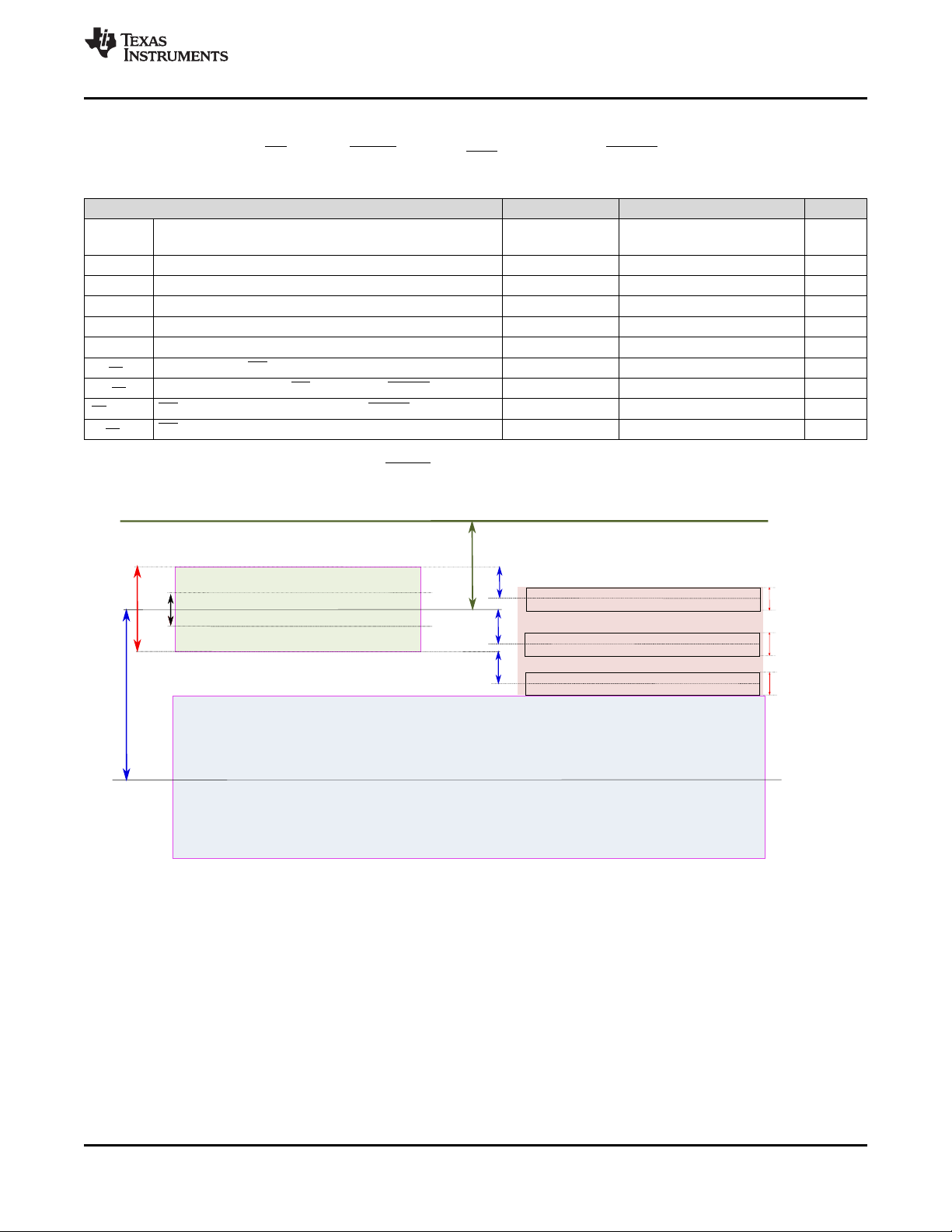
Figure 1. Voltage Threshold and Hysteresis Accuracy
Product Folder Links: TPS3870-Q1
Submit Documentation FeedbackCopyright © 2019, Texas Instruments Incorporated
7
t
D
Hysteresis
V
DD(MIN)
V
POR
UVLO
RESET
t
PD
Undefined
SENSE
V
DD
V
IT+(OV)
V
IT+(OV)
- V
HYS
t
D
t
SD
TPS3870-Q1
SNVSBI5A –JULY 2019–REVISED SEPTEMBER 2019
www.ti.com
(1) VDD= 2 V, RPU= 10 kΩ to V
DD
(2) Variant M (time delay bypass) has a ~40 µs pulse at RESET pin during power up window, this is present only when
the power cycle off time is longer than 10 seconds, this behavior will not occur if SENSE pin is within window of
operation during VDDpower up.
Figure 2. SENSE Timing Diagram
8
Submit Documentation Feedback Copyright © 2019, Texas Instruments Incorporated
Product Folder Links: TPS3870-Q1
Temperature (qC)
Supply Current (PA)
-50 -25 0 25 50 75 100 125
2
3
4
5
6
D008
VDD = 1.7 V
VDD = 3.3 V
VDD = 5.5 V
Overdrive (%)
SENSE Glitch Immunity (Ps)
0 5 10 15 20 25 30 35 40 45 50 55
9
10
11
12
13
14
15
16
D010
-40qC
25qC
125qC
Temperature (qC)
Accuracy (%)
-50 -25 0 25 50 75 100 125
0.5
0.52
0.54
0.56
0.58
0.6
D006
0.8 V
1.2 V
1.8 V
3.3 V
5.0 V
Temperature (qC)
Supply Current (PA)
-50 -25 0 25 50 75 100 125
2
3
4
5
6
7
D007
VDD = 1.7 V
VDD = 3.3 V
VDD = 5.5 V
Temperature (qC)
Accuracy (%)
-50 -25 0 25 50 75 100 125
-0.2
-0.15
-0.1
-0.05
0
0.05
0.1
0.15
0.2
D002
0.8 V
1.2 V
1.8 V
3.3 V
5.0 V
V
IT+(OV)
Accuracy (%)
Frequency (%)
-0.4 -0.3 -0.2 -0.1 0 0.1 0.2 0.3 0.4
0
5
10
15
20
25
30
35
D004
www.ti.com
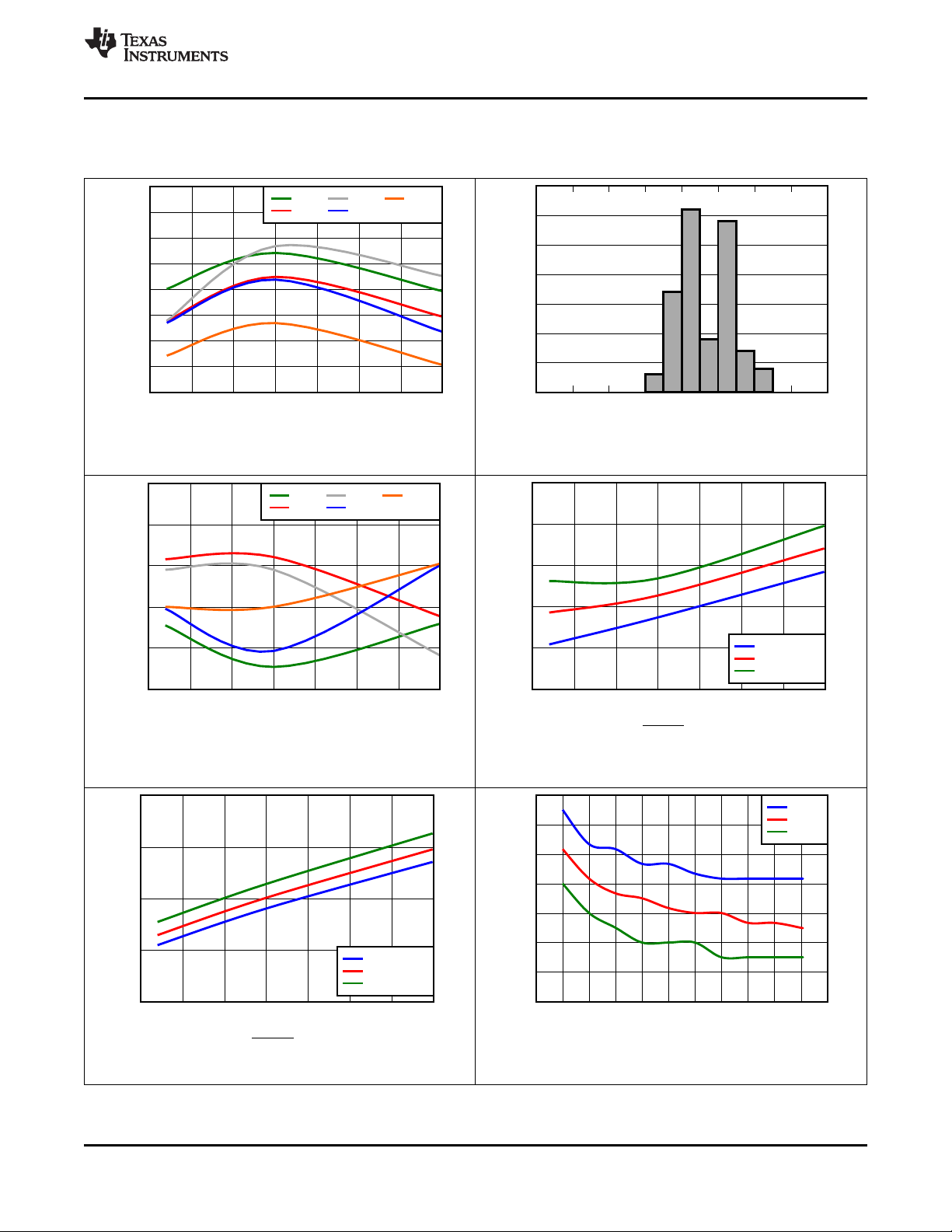
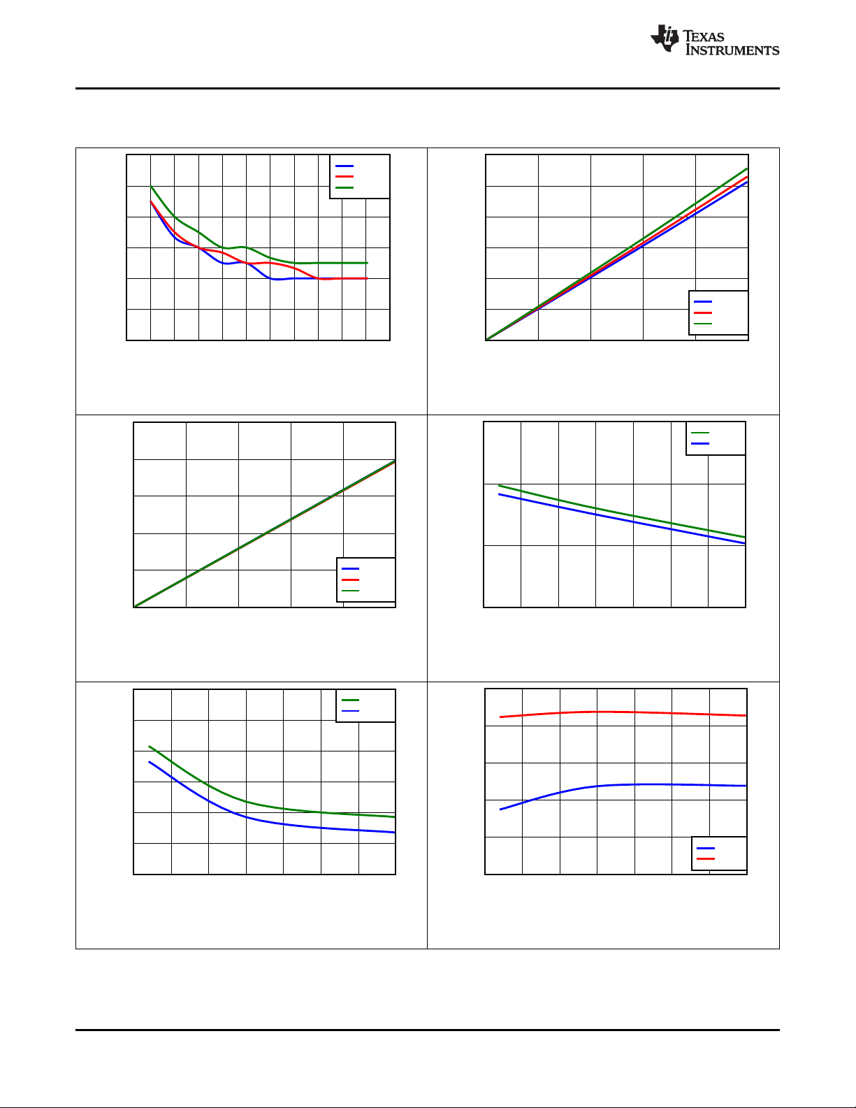
7.7 Typical Characteristics
At TJ= 25°C, VDD= 3.3 V, and RPU= 10 kΩ, unless otherwise noted.
Tested across multiple voltage options
Figure 3. Overvoltage Accuracy vs Temperature Figure 4. Overvoltage Accuracy Distribution
TPS3870-Q1
SNVSBI5A –JULY 2019–REVISED SEPTEMBER 2019
Tested across multiple voltage options
Figure 5. Overvoltage Hysteresis Voltage Accuracy vs
Temperature
Output (RESET Pin) = Low
Figure 7. Supply Current vs Temperature
Product Folder Links: TPS3870-Q1
Output (RESET Pin) = High
Figure 6. Supply Current vs Temperature
VDD = 1.7 V
Figure 8. SENSE Glitch Immunity (VIT+) vs Overdrive
Submit Documentation FeedbackCopyright © 2019, Texas Instruments Incorporated
9
Temperature (qC)
MR Threshold (V)
-50 -25 0 25 50 75 100 125
1.04
1.06
1.08
1.1
1.12
1.14
1.16
D016
V
MR_H
V
MR_L
Temperature (qC)
I
CT
(nA)
-50 -25 0 25 50 75 100 125
365
370
375
380
385
390
D017
1.7 V
5.5 V
I
RESET
(mA)
V
OL
(V)
0 1 2 3 4 5
0
0.05
0.1
0.15
0.2
0.25
D014
-40qC
25qC
125qC
Temperature (qC)
MR Threshold (V)
-50 -25 0 25 50 75 100 125
0.3
0.4
0.5
0.6
D015
V
MR_H
V
MR_L
Overdrive (%)
SENSE Glitch Immunity (Ps)
0 5 10 15 20 25 30 35 40 45 50 55
3
4
5
6
7
8
9
D012
-40qC
25qC
125qC
I
RESET
(mA)
V
OL
(V)
0 1 2 3 4 5
0
0.05
0.1
0.15
0.2
0.25
0.3
D013
-40qC
25qC
125qC
TPS3870-Q1
SNVSBI5A –JULY 2019–REVISED SEPTEMBER 2019
Typical Characteristics (continued)
At TJ= 25°C, VDD= 3.3 V, and RPU= 10 kΩ, unless otherwise noted.
www.ti.com
VDD = 5.5 V
Figure 9. SENSE Glitch Immunity (VIT+) vs Overdrive
VDD = 5.5 V
Figure 11. Low-Level Output Voltage vs RESET current
VDD = 1.7 V
Figure 10. Low-Level Output Voltage vs RESET current
VDD = 1.7 V
Figure 12. SET Threshold vs Temperature
10
Figure 13. SET Threshold vs Temperature Figure 14. CT Current vs CT value
Submit Documentation Feedback Copyright © 2019, Texas Instruments Incorporated
VDD = 5.5 V
Product Folder Links: TPS3870-Q1

Temperature (qC)
t
PD(SENSE)
(Ps)
-50 -25 0 25 50 75 100 125
0
2
4
6
8
10
12
D020
VDD = 1.7 V
VDD = 3.3 V
VDD = 5.5 V
CT (nF)
RESET Timeout (ms)
0.1 1 10 100 1000
0.1
1
10
100
500
D018
-40qC
25qC
125qC
CT (nF)
RESET Timeout (ms)
0.1 1 10
0.1
1
55
D019
-40qC
25qC
125qC
www.ti.com
Typical Characteristics (continued)
At TJ= 25°C, VDD= 3.3 V, and RPU= 10 kΩ, unless otherwise noted.
Figure 15. RESET Timeout vs CT Capacitor Figure 16. Timeout vs CT Capacitor (0.1 to 10 nF)
TPS3870-Q1
SNVSBI5A –JULY 2019–REVISED SEPTEMBER 2019
Figure 17. Detect Propagation Delay vs Temperature
Product Folder Links: TPS3870-Q1
Submit Documentation FeedbackCopyright © 2019, Texas Instruments Incorporated
11
GND
SENSE
RESET
MR
Time Delay
Logic
VDD
R
MR
Vref
VDD
CT
I
CT
Cap
Control
V
CT
50mV
OV Comparator
TPS3870-Q1
SNVSBI5A –JULY 2019–REVISED SEPTEMBER 2019
www.ti.com
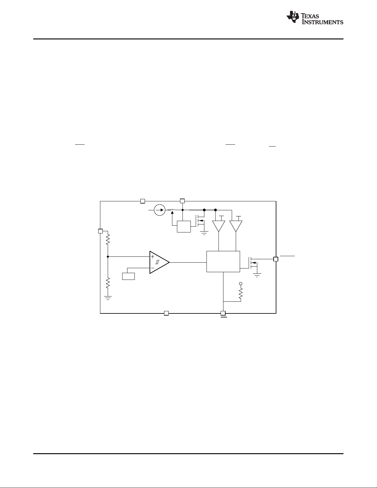
8 Detailed Description
8.1 Overview
The TPS3870-Q1 family of devices uses a voltage comparator and a precision voltage reference for overvoltage
detection. The TPS3870-Q1 features a highly accurate threshold voltage (±0.7% over temperature) and a variety
of voltage threshold variants.
The TPS3870-Q1 includes the resistors used to set the overvoltage threshold internal to the device. These
internal resistors allow for lower component counts and greatly simplifies the design because no additional
margins are needed to account for the accuracy of external resistors.
TPS3870-Q1 versions J, K and L have three time delay settings, two fixed by connecting CT pin to VDD through
a resistor and leaving CT floating and a programmable time delay setting that only requires a single capacitor
connected from CT pin to ground.
Manual Reset (MR) allows for sequencing or hard reset by driving the MR pin below V
The TPS3870-Q1 is designed to assert active low output signals when the monitored voltage is outside the safe
window. The relationship between the monitored voltage and the states of the outputs is shown in Table 2.
8.2 Functional Block Diagram
MR_L
.
*For all possible voltages, threshold tolerance, time delays, and threshold options, see Table 6.
8.3 Feature Description
8.3.1 VDD
The TPS3870-Q1 is designed to operate from an input voltage supply range between 1.7 V to 5.5 V. An input
supply capacitor is not required for this device; however, if the input supply is noisy good analog practice is to
place a 1-µF capacitor between the VDD pin and the GND pin.
VDDneeds to be at or above V
8.3.2 SENSE
The TPS3870-Q1 uses a comparator with a precision reference voltage and a trimmed resistor divider. This
configuration optimizes device accuracy because all resistor tolerances are accounted for in the accuracy and
performance specifications. The comparator also includes built-in hysteresis that provides noise immunity and
ensures stable operation.
12
Submit Documentation Feedback Copyright © 2019, Texas Instruments Incorporated
DD(MIN)
for at least the start-up delay (tSD+ tD) for the device to be fully functional.
Product Folder Links: TPS3870-Q1
V
SENSE
V
IT+(OV)
V
IT+(OV)
- V
HYS
RESET
OV Limit
t
D
t
PD
TPS3870-Q1
www.ti.com
SNVSBI5A –JULY 2019–REVISED SEPTEMBER 2019
Feature Description (continued)
Although not required in most cases, for noisy applications good analog design practice is to place a 1-nF to 10nF bypass capacitor at the SENSE input in order to reduce sensitivity to transient voltages on the monitored
signal.
When monitoring VDD supply voltage, the SENSE pin can be connected directly to VDD. The output (RESET) is
high impedance when voltage at the SENSE pin is lower than the upper boundary of the threshold.
8.3.3 RESET
In a typical TPS3870-Q1 application, the RESET output is connected to a reset or enable input of a processor
[such as a digital signal processor (DSP), application-specific integrated circuit (ASIC), or other processor type]
or the enable input of a voltage regulator [such as a DC-DC converter or low-dropout regulator (LDO)].
The TPS3870-Q1 has an open drain active low output that requires a pull-up resistor to hold these lines high to
the required voltage logic. Connect the pull-up resistor to the proper voltage rail to enable the output to be
connected to other devices at the correct interface voltage levels. To ensure proper voltage levels, give some
consideration when choosing the pull-up resistor values. The pull-up resistor value is determined by VOL, output
capacitive loading, and output leakage current. These values are specified in Specifications. The open drain
output can be connected as a wired-OR logic with other open drain signals such as another TPS3870-Q1
RESET pin.
Table 2 describes the scenarios when the output (RESET) is either asserted low or high impedance.
Figure 18. RESET output
8.3.4 Capacitor Time (CT)
The CT pin provides the user the functionality of both high-precision, factory-programmed, reset delay timing
options and user-programmable, reset delay timing. The CT pin can be pulled up to VDDthrough a resistor, have
an external capacitor to ground, or can be left unconnected. The configuration of the CT pin is re-evaluated by
the device every time the voltage on the SENSE line enters the valid window (V
SENSE
< V
IT+(OV)
). The pin
evaluation is controlled by an internal state machine that determines which option is connected to the CT pin.
The sequence of events takes 450 μs to determine if the CT pin is left unconnected, pulled up through a resistor,
or connected to a capacitor. If the CT pin is being pulled up to VDD, then a pull-up resistor is required, 10 kΩ is
recommended.
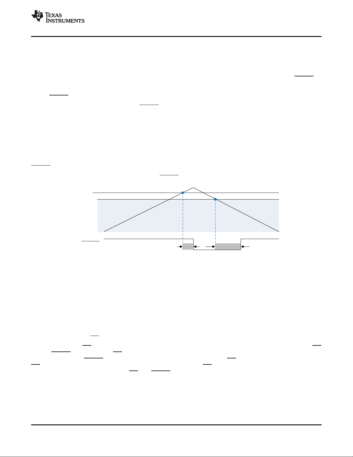
8.3.5 Manual Reset (MR)
The manual reset (MR) input allows a processor or other logic circuits to initiate a reset. A logic low on MR
causes RESET to assert. After MR returns to a logic high and the SENSE pin voltage is within a valid condition
(V
SENSE
< V
) , RESET is deasserted after the reset delay time (tD). If MR is not controlled externally, then
IT+(OV)
MR can either be connected to VDDor left floating because the MR pin is internally pulled up to VDD. Figure
Figure 19 shows the relation between MR and RESET.
Submit Documentation FeedbackCopyright © 2019, Texas Instruments Incorporated
Product Folder Links: TPS3870-Q1
13

V
IT+(OV)
V
IT+(OV)
- V
HYS
Hysteresis
t
D(MR)
V
MR_L
t
MR_W
Pulse < t
GI (MR)
t
PD (MR)
RESET
SENSE
Pulse < V
MR_L
MR
V
MR_H
TPS3870-Q1
SNVSBI5A –JULY 2019–REVISED SEPTEMBER 2019
Feature Description (continued)
www.ti.com
(1) RESET pulls up to VDD with 10 kΩ.
(2) To initiate and continue time reset counter both conditions must be met MR pin above V
below V
IT+(OV)
- V
HYS
or floating and V
MR_H
SENSE
(3) MR is ignored during output RESET low event
Figure 19. Manual Reset Timing Diagram
8.4 Device Functional Modes
Table 2. Functional Mode Truth Table
DESCRIPTION CONDITION MR PIN VDD PIN OUTPUT (RESET PIN)
Normal Operation SENSE < V
Over Voltage
detection
SENSE > V
Manual reset SENSE < V
UVLO engaged SENSE < V
8.4.1 Normal Operation (VDD> V
When the voltage on VDDis greater than V
correspond to the SENSE pin voltage with respect to the threshold limits, when SENSE voltage is outside of
threshold limits the RESET voltage will be low (VOL).
8.4.2 Undervoltage Lockout (V
IT+(OV)
IT+(OV)
IT+(OV)
IT+(OV)
DD(MIN)
< VDD< UVLO)
POR
When the voltage on VDDis less than the device UVLO voltage but greater than the power-on reset voltage
(V
), the RESET pin will be held low , regardless of the voltage on SENSE pin.
POR
Open or above V
Open or above V
Below V
Open or above V
)
DD(MIN)
MR_L
MR_H
MR_H
MR_H
VDD> V
DD(MIN)
VDD> V
DD(MIN)
VDD> V
DD(MIN)
V
< VDD< UVLO Low
POR
High
for approximately (tSD+ tD), the RESET output state will
Low
Low
8.4.3 Power-On Reset (VDD< V
When the voltage on VDDis lower than the required voltage (V
POR
)
) to internally pull the asserted output to GND,
POR
RESET signal is undefined and is not to be relied upon for proper device function.
14
Submit Documentation Feedback Copyright © 2019, Texas Instruments Incorporated
Product Folder Links: TPS3870-Q1

DC/DC nominal output
Regulator output voltage accuracy
Margin for ripple and transients
0.7% Allowed threshold tolerance
- 0.7% Minimum system voltage
0%
4%
5%
Potential Failure or Malfunction
+
Supply
Voltage
Margin
Voltage
Threshold
Accuracy
TPS3870-Q1
www.ti.com
SNVSBI5A –JULY 2019–REVISED SEPTEMBER 2019
9 Application and Implementation
NOTE
Information in the following applications sections is not part of the TI component
specification, and TI does not warrant its accuracy or completeness. TI’s customers are
responsible for determining suitability of components for their purposes. Customers should
validate and test their design implementation to confirm system functionality.
9.1 Application Information
9.1.1 Voltage Threshold Accuracy
Voltage monitoring requirements vary depending on the voltage supply tolerance of the device being powered.
Due to the high precision of the TPS3870-Q1 (±0.7% Max), the device allows for a wider supply voltage margins
and threshold headroom for tight tolerance applications.
For example, take a DC/DC regulator providing power to a core voltage rail of an MCU. The MCU has a
tolerance of ±5% of the nominal output voltage of the DC/DC. The user sets an ideal voltage threshold of 4%
which allows for ±1% of threshold accuracy. Since the TPS3870-Q1 threshold accuracy is higher than ±1%, the
user has more supply voltage margin which can allow for a relaxed power supply design. This gives flexibility to
the DC/DC to use a smaller output capacitor or inductor because of a larger voltage window for voltage ripple
and transients. There is also headroom between the minimum system voltage and voltage tolerance of the MCU
to ensure that the voltage supply will never be in the region of potential failure of malfunction without the
TPS3870-Q1 asserting a reset signal.
Figure 20 illustrates the supply overvoltage margin and accuracy of the TPS3870-Q1 for the example explained
above. Using a low accuracy supervisor will eat into the available budget for the power supply ripple and
transient response. This gives less flexibility to the user and a more stringent DC/DC converter design.
Figure 20. TPS3870-Q1 Voltage Threshold Accuracy
Product Folder Links: TPS3870-Q1
Submit Documentation FeedbackCopyright © 2019, Texas Instruments Incorporated
15

VDD
I
CT
CT
VDD
CT
10 k
CT
User Programmable
Capacitor to GND
10 NŸ5HVLVWRUWR9''
CT Unconnected
VDD
VDD
I
CT
VDD
I
CT
VDD
Cap
Control
Cap
Control
Cap
Control
TPS3870-Q1
SNVSBI5A –JULY 2019–REVISED SEPTEMBER 2019
www.ti.com
Application Information (continued)
9.1.2 CT Reset Time Delay
The TPS3870-Q1 features three options for setting the reset delay (tD): connecting a capacitor to the CT pin,
connecting a pull-up resistor to VDD, and leaving the CT pin unconnected. Figure 21 shows a schematic drawing
of all three options. To determine which option is connected to the CT pin, an internal state machine controls the
internal pulldown device and measures the pin voltage. This sequence of events takes 450 μs to determine
which timing option is used. Every time the voltage on the SENSE line enters the valid window (V
-V
, the state machine determines the CT option.
HYS
SENSE
< V
IT+(OV)
Figure 21. CT Charging Circuit
9.1.2.1 Factory-Programmed Reset Delay Timing
To use the factory-programmed timing options, the CT pin must either be left unconnected or pulled up to VDD
through a 10 kΩ pull-up resistor. Using these options enables a high-precision reset delay timing, as shown in
Table 3.
Table 3. Reset Delay Time for Factory-Programmed Reset Delay Timing
VARIANT
TPS3870J Programmable t
TPS3870K Programmable t
TPS3870L Programmable t
TPS3870M N/A 50 50 µs
CT = Capacitor to GND CT = Floating CT = 10 kΩ to VDD
D
D
D
RESET DELAY TIME (tD)
10 200 ms
1 20 ms
5 100 ms
VALUE
9.1.2.2 Programmable Reset Delay-Timing
The TPS3870 reset time delay is based on internal current source (ICT) to charge external capacitor (CCT) and
read capacitor voltage with the internal comparator. The minimum value capacitor is 250 pF. There is no
limitation on maximum capacitor the only constrain is imposed by the initial voltage of the capacitor, if CT cap is
zero or near to zero then ideally there is no other constraint on the max capacitor. The typical ideal capacitor
value needed for a given delay time can be calculated using Equation 1, where CCTis in nanofarads (nF) and t
is in ms:
tD= 3.066 × CCT+ 0.5 ms (1)
To calculate the minimum and maximum-reset delay time use Equation 2 and Equation 3, respectively.
t
= 2.7427 × CCT+ 0.3 ms (2)
D(min)
t
= 3.4636 × CCT+ 0.7 ms (3)
D(max)
D
16
Submit Documentation Feedback Copyright © 2019, Texas Instruments Incorporated
Product Folder Links: TPS3870-Q1

VDD
I
CT
CT
10 kResistor to
GND to Latch
VDD
Cap
Control
10 k
Voltage at CT
to Unlatch
10 k
V > V
CT
TPS3870-Q1
www.ti.com
SNVSBI5A –JULY 2019–REVISED SEPTEMBER 2019
The slope of the equation is determined by the time the CT charging current (ICT) takes to charge the external
capacitor up to the CT comparator threshold voltage (VCT). When RESET is asserted, the capacitor is discharged
through the internal CT pulldown resistor. When the RESET conditions are cleared, the internal precision current
source is enabled and begins to charge the external capacitor; when VCT= 1.15 V, RESET is unasserted. Note
that in order to minimize the difference between the calculated RESET delay time and the actual RESET delay
time, use a use a high-quality ceramic dielectric COG, X5R, or X7R capacitor and minimize parasitic board
capacitance around this pin. Table 4 lists the reset delay time ideal capacitor values for CCT.
Table 4. Reset Delay Time for Ideal Capacitor Values
C
CT
250 pF 1.27 ms
1 nF 3.57 ms
3.26 nF 10.5 ms
32.6 nF 100.45 ms
65.2 nF 200.40 ms
1uF 3066.50 ms
RESET DELAY TIME (tD), TYPICAL
9.1.3 RESET Latch Mode
The TPS3870-Q1 features a voltage latch mode on the RESET pin when connecting the CT pin to common
ground . A pull-down resistor is recommended to limit current consumption of the system. In latch mode, if the
RESET pin is low or triggers low, the pin will stay low regardless if V
boundaries (V
SENSE
< V
). To unlatch the device provide a voltage to the CT pin that is greater than the CT
IT+(OV)
is within the acceptable voltage
SENSE
pin comparator threshold voltage, VCT. The RESET pin will trigger high instantaneously without any reset delay.
A voltage greater than 1.2 V to recommended to ensure a proper unlatch. Use a series resistance to limit current
when an unlatch voltage is applied. For more information, Design 1: RESET Latch Mode gives an example of a
typical latch application.
NOTE
At power up, the TPS3870-Q1 will be latched when CT is connected to GND. To ensure
correct power up when using RESET latch mode, send a pulse to the CT pin greater than
1.2 V after tSDand SENSE is within the correct window of operation.
Figure 22. RESET Latch Circuit
Product Folder Links: TPS3870-Q1
Submit Documentation FeedbackCopyright © 2019, Texas Instruments Incorporated
17

MR
TPS3870-Q1
SENSE RESET
VDD
CT GND
VDD
VDD
R2
10 lQ
R1
V
MON
V
sense
TPS3870-Q1
SNVSBI5A –JULY 2019–REVISED SEPTEMBER 2019
www.ti.com
9.1.4 Adjustable Voltage Thresholds
The TPS3870-Q1 0.7% maximum accuracy allows for adjustable voltage thresholds using external resistors
without adding major inaccuracies to the device. In case that the desired monitored voltage is not available,
external resistor dividers can be used to set the desired voltage thresholds. Figure 23 illustrates an example of
how to adjust the voltage threshold with external resistor dividers. The resistors can be calculated depending on
the desired voltage threshold and device part number. TI recommends using the 0.8V voltage threshold device
such as the TPS3870J4080 because of the bypass mode of internal resistor ladder.
For example, consider a 2.0 V rail being monitored (V
R1 = 15 kΩ given that R2 = 10 kΩ, V
= 2 V , and V
MON
0.8 V rail with a +4% voltage threshold. This means that the device overvoltage threshold (V
Using Equation 4, the monitored overvoltage threshold (V
) using the TPS3870J4080 variant. Using Equation 4,
MON
= 0.8 V. This device is typically meant to monitor a
SENSE
) = 2.08 V when V
MON+
SENSE
= V
IT+(OV)
IT+(OV)
) is 0.832 V.
. If a wider
tolerance threshold is desired, use a device variant shown on Table 6 to determine what device part number
matches your application.
V
= V
SENSE
× (R2÷ (R1+ R2)) (4)
MON
There are inaccuracies that must be taken into consideration while adjusting voltage thresholds. Aside from the
tolerance of the resistor divider, there is an internal resistance of the SENSE pin that may affect the accuracy of
the resistor divider. Although expected to be very high impedance, users are recommended to calculate the
values for design specifications. The internal sense resistance (R
(V
) divided by the sense current (I
SENSE
) as shown in Equation 6. V
SENSE
Equation 4 depending on the resistor divider and monitored voltage. I
I
SENSE
R
SENSE
= (V
= V
MON
SENSE
– V
÷ I
SENSE
SENSE
) ÷ R1– (V
÷ R2) (5)
SENSE
) can be calculated by the sense voltage
SENSE
SENSE
SENSE
can be calculated using Equation 5.
can be calculated using
(6)
Figure 23. Adjustable Voltage Threshold with External Resistor Dividers
Although Equation 4 solves for V
, inaccuracies for leakage need to be taken into consideration when
SENSE
understanding the overall threshold accuracy of the device. To calculate the threshold with this inaccuracy taken
into account, use Equation 7
V
To calculate the worst case values through the resistor divider, I
IT_Actual
= V
SENSE
+ R1× ((V
SENSE
÷ R2) + I
) (7)
SENSE
should be taken from the Electrical
SENSE
Characteristics table. While these equations provide a summary of what you need to correctly account for factors
that go into determining your resistor divider with inaccuracy, you should use the Application Report Optimizing
Resistor Dividers at a Comparator Input to further understand this and to design your implementation. This report
explains how to optimize the resistor divider at the SENSE input for an adjustable voltage threshold version of
the device. You should follow this Application Report using 0.8 V as the V
18
Submit Documentation Feedback Copyright © 2019, Texas Instruments Incorporated
Product Folder Links: TPS3870-Q1
value for the TPS3870-Q1.
REF

V
RESET
V
SENSE
VIT+(OV) - VHYS VIT+(OV)
TPS3870-Q1
www.ti.com
SNVSBI5A –JULY 2019–REVISED SEPTEMBER 2019
9.1.5 Immunity to SENSE Pin Voltage Transients
The TPS3870-Q1 is immune to short voltage transient spikes on the input pins. Sensitivity to transients depends
on both transient duration and overdrive (amplitude) of the transient.
Overdrive is defined by how much the V
exceeds the specified threshold, and is important to know because
SENSE
the smaller the overdrive, the slower the response of the outputs (RESET). Threshold overdrive is calculated as
a percent of the threshold in question, as shown in Equation 8:
Overdrive % = | (V
SENSE
- (V
)) / VIT(Nominal) × 100% |
IT+(OV)
where:
• V
• VIT(Nominal) is the nominal threshold voltage
• V
is the voltage at the SENSE pin
SENSE
represents the actual overvoltage tripping voltage (8)
IT+(OV)
9.1.5.1 Hysteresis
The overvoltage comparator includes built-in hysteresis that provides noise immunity and ensures stable
operation. For example if the voltage on the SENSE pin goes above V
and RESET is asserted (driven low),
IT+(OV)
then when the voltage on the SENSE pin is below the positive threshold voltage, RESET deasserts after the
user-defined RESET delay time. Figure Figure 24 shows the relation between V
(V
).
HYS
and hysteresis voltage
IT+(OV)
Figure 24. SENSE Pin Hysteresis
Product Folder Links: TPS3870-Q1
Submit Documentation FeedbackCopyright © 2019, Texas Instruments Incorporated
19

MR
TPS3870-Q1
SENSE RESET
VDD
CT GND
VDD
VDD
V
GPIO
V
CORE
V
CORE
Microcontroller
10 lQ
Microcontroller
V
GPIO
10 lQ
10 lQ
TPS3870-Q1
SNVSBI5A –JULY 2019–REVISED SEPTEMBER 2019
www.ti.com
9.2 Typical Application
9.2.1 Design 1: RESET Latch Mode
Another typical application for the TPS3870-Q1 is shown in Figure 25. The TPS3870-Q1 is used in a RESET
latch output mode. In latch mode, once RESET driven logic low, it will stay low regardless of the sense voltage. If
the RESET pin is low on start up, it will also stay low regardless of sense voltage.
Figure 25. Window Voltage Monitoring with RESET Latch
9.2.1.1 Design Requirements
Table 5. Design Parameters
PARAMETER DESIGN REQUIREMENT DESIGN RESULT
Monitored Rail
Output logic voltage 5-V CMOS 5-V CMOS
Maximum device current
consumption
1.2-V
1.2 V (including device accuracy), Latch when
RESET is low, until voltage is applied on CT pin.
nominal, with alerts if outside of 5% of
CORE
15 µA 4.5 µA (Typ), 7 µA (Max)
Worst case V
= 1.256 V (4.7%),
IT+(OV)
9.2.1.2 Detailed Design Procedure
The RESET pin can be latched when the CT pin is connected to a common ground with a pull-down resistor. A
10 kΩ resistors is recommended to limit current consumption. To unlatch the device provide a voltage to the CT
pin that is greater than the CT pin comparator threshold voltage, VCT. A voltage greater than 1.15 V to
recommended to ensure a proper unlatch. Use a series resistance to limit current when an unlatch voltage is
applied. To go back into latch operation, disconnect the voltage on the CT pin. The RESET pin will trigger high
instantaneously without any reset delay.
20
Submit Documentation Feedback Copyright © 2019, Texas Instruments Incorporated
Product Folder Links: TPS3870-Q1

www.ti.com
9.2.1.3 Application Curves
V
ramp from 0 V to 1.4V, VDD= 3.3 V, VCT= 0 V
SENSE
Figure 26. TPS3870-Q1 SENSE Ramp Latch Function
V
RESET
= VDD = 3.3 V
TPS3870-Q1
SNVSBI5A –JULY 2019–REVISED SEPTEMBER 2019
VCTbiased at least to 1.15 V , V
V
= VDD = 3.3 V
RESET
Figure 27. TPS3870-Q1 CT Bias Unlatch Function
SENSE
= 1.2 V
VDDramp up from 0 V to 3.3 V , V
V
= VDD = 3.3 V
RESET
= 1.2 V, CT = 0 V
SENSE
Figure 28. TPS3870-Q1 VDD Ramp Latch Function
Product Folder Links: TPS3870-Q1
Submit Documentation FeedbackCopyright © 2019, Texas Instruments Incorporated
21

Sense
VDD
CT
MR
GND
RESET
1 …F
VDD
V_Sense
GND
Pull-Up Voltage
10 NŸ
TPS3870-Q1
SNVSBI5A –JULY 2019–REVISED SEPTEMBER 2019
www.ti.com
10 Power Supply Recommendations
10.1 Power Supply Guidelines
This device is designed to operate from an input supply with a voltage range between 1.7 V to 5.5 V. It has a 6-V
absolute maximum rating on the VDD pin. It is good analog practice to place a 0.1-µF to 1-µF capacitor between
the VDD pin and the GND pin depending on the input voltage supply noise. If the voltage supply providing power
to VDD is susceptible to any large voltage transient that exceed maximum specifications, additional precautions
must be taken. See SNVA849 for more information.
11 Layout
11.1 Layout Guidelines
• Place the external components as close to the device as possible. This configuration prevents parasitic errors
from occurring.
• Avoid using long traces for the VDD supply node. The VDD capacitor, along with parasitic inductance from
the supply to the capacitor, can form an LC circuit and create ringing with peak voltages above the maximum
VDD voltage.
• Avoid using long traces of voltage to the sense pin. Long traces increase parasitic inductance and cause
inaccurate monitoring and diagnostics.
• Do not run sensitive analog traces in parallel with digital traces. Avoid crossing digital and analog traces if
possible, and only make perpendicular crossings when absolutely necessary.
11.2 Layout Example
Figure 29. Recommended Layout
22
Submit Documentation Feedback Copyright © 2019, Texas Instruments Incorporated
Product Folder Links: TPS3870-Q1

www.ti.com
SNVSBI5A –JULY 2019–REVISED SEPTEMBER 2019
12 Device and Documentation Support
12.1 Device Nomenclature
Table 6 shows how to decode the function of the device based on its part number.
Table 6. Device Naming Convention
DESCRIPTION NOMENCLATURE VALUE
TPS3870 TPS3870
J
Time delay options: Every part
has two fixed time delay and
adjustable delay option via
external capacitor Part number
Tolerance options: Trigger or threshold
voltage as a percentage of the monitored
threshold voltage
Nominal monitor threshold voltage option 050 0.50 V
Package DSE WSON - 6 pin (1.5 mm × 1.5 mm)
Reel R Large reel
Automotive version Q1 Q100 AEC
OV Only
K
L
M
3 Overvoltage threshold from nominal value = OV : 3%
4 Overvoltage threshold from nominal value = OV : 4%
5 Overvoltage threshold from nominal value = OV : 5%
6 Overvoltage threshold from nominal value = OV : 6%
7 Overvoltage threshold from nominal value = OV : 7%
055 0.55 V
060 0.60 V
065 0.65 V
070 0.70 V
075 0.75 V
080 0.80 V
085 0.85 V
090 0.90 V
095 0.95 V
100 1.00 V
105 1.05 V
110 1.10 V
115 1.15 V
120 1.20 V
125 1.25 V
130 1.30 V
150 1.50 V
180 1.80 V
250 2.50 V
280 2.80 V
290 2.90 V
330 3.30 V
500 5.00 V
CT pin open = 10 ms, CT pin tied to VDD = 200 ms
CT programable with external capacitor
CT pin open = 1 ms, CT pin tied to VDD = 20 ms
CT programable with external capacitor
CT pin open = 5 ms, CT pin tied to VDD = 100 ms
CT programable with external capacitor
CT pin open = 50 µs, CT pin tied to VDD = 50 µs
CT not programable
TPS3870-Q1
Product Folder Links: TPS3870-Q1
Submit Documentation FeedbackCopyright © 2019, Texas Instruments Incorporated
23

TPS3870-Q1
SNVSBI5A –JULY 2019–REVISED SEPTEMBER 2019
www.ti.com
12.2 Documentation Support
12.2.1 Evaluation Module
An evaluation module (EVM) is available to assist in the initial circuit performance evaluation using the TPS3870Q1. The EVM for the TPS3703-Q1 can be used to evaluate the TPS3870-Q1 for just overvoltage only. The
TPS3703-Q1 evaluation module (and related user guide) can be requested at the Texas Instruments website
through the product folders or purchased directly from the TI eStore .
12.3 Receiving Notification of Documentation Updates
To receive notification of documentation updates, navigate to the device product folder on ti.com. In the upper
right corner, click on Alert me to register and receive a weekly digest of any product information that has
changed. For change details, review the revision history included in any revised document.
12.4 Support Resources
TI E2E™ support forums are an engineer's go-to source for fast, verified answers and design help — straight
from the experts. Search existing answers or ask your own question to get the quick design help you need.
Linked content is provided "AS IS" by the respective contributors. They do not constitute TI specifications and do
not necessarily reflect TI's views; see TI's Terms of Use.
12.5 Trademarks
E2E is a trademark of Texas Instruments.
All other trademarks are the property of their respective owners.
12.6 Electrostatic Discharge Caution
This integrated circuit can be damaged by ESD. Texas Instruments recommends that all integrated circuits be handled with
appropriate precautions. Failure to observe proper handling and installation procedures can cause damage.
ESD damage can range from subtle performance degradation to complete device failure. Precision integrated circuits may be more
susceptible to damage because very small parametric changes could cause the device not to meet its published specifications.
12.7 Glossary
SLYZ022 — TI Glossary.
This glossary lists and explains terms, acronyms, and definitions.
13 Mechanical, Packaging, and Orderable Information
The following pages include mechanical, packaging, and orderable information. This information is the most
current data available for the designated devices. This data is subject to change without notice and revision of
this document. For browser-based versions of this data sheet, refer to the left-hand navigation.
24
Submit Documentation Feedback Copyright © 2019, Texas Instruments Incorporated
Product Folder Links: TPS3870-Q1
PACKAGE OPTION ADDENDUM
www.ti.com
10-Dec-2020
PACKAGING INFORMATION
Orderable Device Status
TPS3870J4080DSERQ1 ACTIVE WSON DSE 6 3000 RoHS & Green NIPDAUAG Level-1-260C-UNLIM -40 to 125 H5
TPS3870J4330DSERQ1 ACTIVE WSON DSE 6 3000 RoHS & Green NIPDAUAG Level-1-260C-UNLIM -40 to 125 H4
(1)
The marketing status values are defined as follows:
ACTIVE: Product device recommended for new designs.
LIFEBUY: TI has announced that the device will be discontinued, and a lifetime-buy period is in effect.
NRND: Not recommended for new designs. Device is in production to support existing customers, but TI does not recommend using this part in a new design.
PREVIEW: Device has been announced but is not in production. Samples may or may not be available.
OBSOLETE: TI has discontinued the production of the device.
Package Type Package
(1)
Drawing
Pins Package
Qty
Eco Plan
(2)
Lead finish/
Ball material
(6)
MSL Peak Temp
(3)
Op Temp (°C) Device Marking
(4/5)
(2)
RoHS: TI defines "RoHS" to mean semiconductor products that are compliant with the current EU RoHS requirements for all 10 RoHS substances, including the requirement that RoHS substance
do not exceed 0.1% by weight in homogeneous materials. Where designed to be soldered at high temperatures, "RoHS" products are suitable for use in specified lead-free processes. TI may
reference these types of products as "Pb-Free".
RoHS Exempt: TI defines "RoHS Exempt" to mean products that contain lead but are compliant with EU RoHS pursuant to a specific EU RoHS exemption.
Green: TI defines "Green" to mean the content of Chlorine (Cl) and Bromine (Br) based flame retardants meet JS709B low halogen requirements of <=1000ppm threshold. Antimony trioxide based
flame retardants must also meet the <=1000ppm threshold requirement.
(3)
MSL, Peak Temp. - The Moisture Sensitivity Level rating according to the JEDEC industry standard classifications, and peak solder temperature.
(4)
There may be additional marking, which relates to the logo, the lot trace code information, or the environmental category on the device.
(5)
Multiple Device Markings will be inside parentheses. Only one Device Marking contained in parentheses and separated by a "~" will appear on a device. If a line is indented then it is a continuation
of the previous line and the two combined represent the entire Device Marking for that device.
(6)
Lead finish/Ball material - Orderable Devices may have multiple material finish options. Finish options are separated by a vertical ruled line. Lead finish/Ball material values may wrap to two
lines if the finish value exceeds the maximum column width.
Important Information and Disclaimer:The information provided on this page represents TI's knowledge and belief as of the date that it is provided. TI bases its knowledge and belief on information
provided by third parties, and makes no representation or warranty as to the accuracy of such information. Efforts are underway to better integrate information from third parties. TI has taken and
continues to take reasonable steps to provide representative and accurate information but may not have conducted destructive testing or chemical analysis on incoming materials and chemicals.
TI and TI suppliers consider certain information to be proprietary, and thus CAS numbers and other limited information may not be available for release.
In no event shall TI's liability arising out of such information exceed the total purchase price of the TI part(s) at issue in this document sold by TI to Customer on an annual basis.
Samples
Addendum-Page 1

PACKAGE OPTION ADDENDUM
www.ti.com
10-Dec-2020
Addendum-Page 2

PACKAGE MATERIALS INFORMATION
www.ti.com 22-Sep-2019
TAPE AND REEL INFORMATION
*All dimensions are nominal
Device Package
TPS3870J4080DSERQ1 WSON DSE 6 3000 178.0 8.4 1.7 1.7 0.95 4.0 8.0 Q2
TPS3870J4330DSERQ1 WSON DSE 6 3000 178.0 8.4 1.7 1.7 0.95 4.0 8.0 Q2
Type
Package
Drawing
Pins SPQ Reel
Diameter
(mm)
Reel
Width
W1 (mm)
A0
(mm)B0(mm)K0(mm)P1(mm)W(mm)
Quadrant
Pin1
Pack Materials-Page 1
PACKAGE MATERIALS INFORMATION
www.ti.com 22-Sep-2019
*All dimensions are nominal
Device Package Type Package Drawing Pins SPQ Length (mm) Width (mm) Height (mm)
TPS3870J4080DSERQ1 WSON DSE 6 3000 205.0 200.0 33.0
TPS3870J4330DSERQ1 WSON DSE 6 3000 205.0 200.0 33.0
Pack Materials-Page 2


IMPORTANT NOTICE AND DISCLAIMER
TI PROVIDES TECHNICAL AND RELIABILITY DATA (INCLUDING DATASHEETS), DESIGN RESOURCES (INCLUDING REFERENCE
DESIGNS), APPLICATION OR OTHER DESIGN ADVICE, WEB TOOLS, SAFETY INFORMATION, AND OTHER RESOURCES “AS IS”
AND WITH ALL FAULTS, AND DISCLAIMS ALL WARRANTIES, EXPRESS AND IMPLIED, INCLUDING WITHOUT LIMITATION ANY
IMPLIED WARRANTIES OF MERCHANTABILITY, FITNESS FOR A PARTICULAR PURPOSE OR NON-INFRINGEMENT OF THIRD
PARTY INTELLECTUAL PROPERTY RIGHTS.
These resources are intended for skilled developers designing with TI products. You are solely responsible for (1) selecting the appropriate
TI products for your application, (2) designing, validating and testing your application, and (3) ensuring your application meets applicable
standards, and any other safety, security, or other requirements. These resources are subject to change without notice. TI grants you
permission to use these resources only for development of an application that uses the TI products described in the resource. Other
reproduction and display of these resources is prohibited. No license is granted to any other TI intellectual property right or to any third
party intellectual property right. TI disclaims responsibility for, and you will fully indemnify TI and its representatives against, any claims,
damages, costs, losses, and liabilities arising out of your use of these resources.
TI’s products are provided subject to TI’s Terms of Sale (www.ti.com/legal/termsofsale.html) or other applicable terms available either on
ti.com or provided in conjunction with such TI products. TI’s provision of these resources does not expand or otherwise alter TI’s applicable
warranties or warranty disclaimers for TI products.
Mailing Address: Texas Instruments, Post Office Box 655303, Dallas, Texas 75265
Copyright © 2020, Texas Instruments Incorporated
 Loading...