

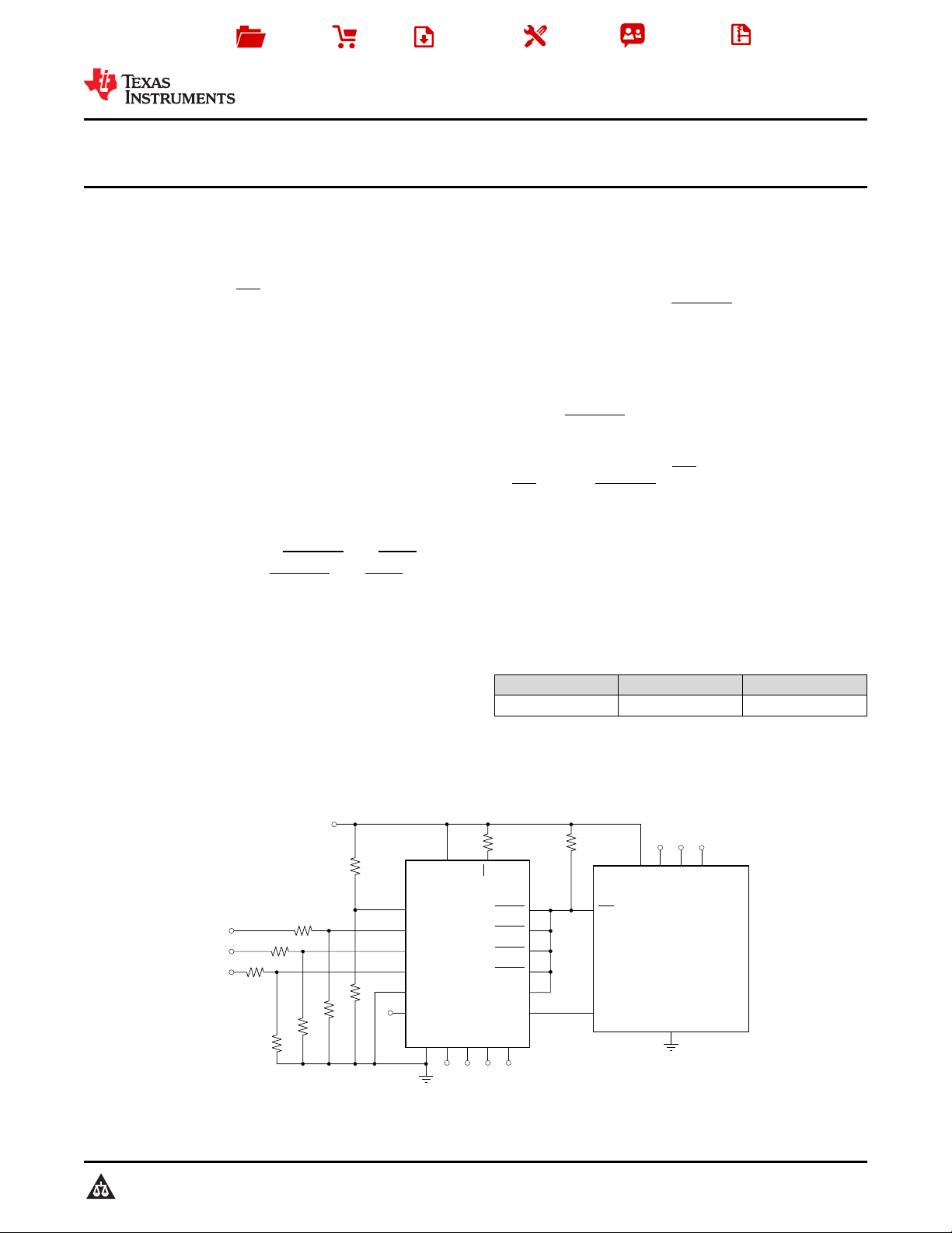
V
MON(1)
RST
TPS386000
SENSE1
SENSE2
SENSE3
SENSE4L
SENSE4H
VREF
GPIO
R
S1H
Microprocessor
DSP
FPGA
GND
CT1
CT2
CT3
CT4
RESET1
RESET2
RESET3
RESET4
WDO
WDI
V
MR
DD
V
V
V
V
DD1
DD2
DD3
DD4
V
V
V
MON(2)
MON(3)
MON(4)
R
S2H
R
S3H
V
V
V
MON(2)
MON(3)
MON(4)
R
S4H
R
S4L
R
S3L
R
S2L
R
S1L
Product
Folder
Order
Now
Technical
Documents
Tools &
Software
Support &
Community
Reference
Design
TPS386000,TPS386040
SBVS105F –SEPTEMBER 2009–REVISED OCTOBER 2018
TPS386000 and TPS386040 Quad Supply Voltage Supervisors
With Adjustable Delay and Watchdog Timer
1 Features
1
• Four Independent Voltage Supervisors
• Channel 1:
– Adjustable Threshold Down to 0.4 V
– Manual Reset (MR) Input
• Channels 2, 3:
– Adjustable Threshold Down to 0.4 V
• Channel 4:
– Adjustable Threshold at Any Positive or
Negative Voltage
– Window Comparator
• Adjustable Delay Time: 1.4 ms to 10 s
• Threshold Accuracy: 0.25% Typical
• Very Low Quiescent Current: 11 μA Typical
• Watchdog Timer With Dedicated Output
• Well-Controlled Output During Power Up
• TPS386000: Open-Drain RESETn and WDO
• TPS386040: Push-Pull RESETn and WDO
• Package: 4-mm × 4-mm, 20-Pin VQFN
2 Applications
• All DSP and Microcontroller Applications
• All FPGA and ASIC Applications
• Telecom and Wireless Infrastructure
• Industrial Equipment
• Analog Sequencing
3 Description
The TPS3860x0 family of supply voltage supervisors
(SVSs) can monitor four power rails that are greater
than 0.4 V and one power rail less than 0.4 V
(including negative voltage) with a 0.25% (typical)
threshold accuracy. Each of the four supervisory
circuits (SVS-n) assert a RESETn or RESETn output
signal when the SENSEm input voltage drops below
the programmed threshold. With external resistors,
the threshold of each SVS-n can be programmed
(where n = 1, 2, 3, 4 and m = 1, 2, 3, 4L, 4H).
Each SVS-n has a programmable delay before
releasing RESETn or RESETn. The delay time can
be set independently for each SVS from 1.4 ms to 10
s through the CTn pin connection. Only SVS-1 has an
active-low manual reset (MR) input; a logic-low input
to MR asserts RESET1 or RESET1.
SVS-4 monitors the threshold window using two
comparators. The extra comparator can be
configured as a fifth SVS to monitor negative voltage
with voltage reference output VREF.
The TPS3860x0 has a very low quiescent current of
11 μA (typical) and is available in a small, 4-mm x 4mm, VQFN-20 package.
Device Information
PART NUMBER PACKAGE BODY SIZE (NOM)
TPS3860x0 VQFN (20) 4.00 mm × 4.00 mm
(1) For all available packages, see the orderable addendum at
the end of the data sheet.
(1)
TPS386000 Typical Application Circuit:
Monitoring Supplies for an FPGA
1
An IMPORTANT NOTICE at the end of this data sheet addresses availability, warranty, changes, use in safety-critical applications,
intellectual property matters and other important disclaimers. PRODUCTION DATA.

TPS386000,TPS386040
SBVS105F –SEPTEMBER 2009–REVISED OCTOBER 2018
www.ti.com
Table of Contents
1 Features.................................................................. 1
2 Applications ........................................................... 1
3 Description ............................................................. 1
4 Revision History..................................................... 2
5 Pin Configuration and Functions......................... 4
6 Specifications......................................................... 6
6.1 Absolute Maximum Ratings ..................................... 6
6.2 ESD Ratings.............................................................. 6
6.3 Recommended Operating Conditions....................... 6
6.4 Thermal Information.................................................. 6
6.5 Electrical Characteristics........................................... 7
6.6 Timing Requirements................................................ 8
6.7 Switching Characteristics.......................................... 8
6.8 Typical Characteristics............................................ 14
7 Parameter Measurement Information ................ 18
8 Detailed Description............................................ 19
8.1 Overview ................................................................. 19
8.2 Functional Block Diagrams ..................................... 20
8.3 Feature Description................................................. 22
8.4 Device Functional Modes........................................ 23
9 Application and Implementation ........................ 25
9.1 Application Information............................................ 25
9.2 Typical Application.................................................. 28
10 Power Supply Recommendations ..................... 29
11 Layout................................................................... 30
11.1 Layout Guidelines ................................................. 30
11.2 Layout Example .................................................... 30
12 Device and Documentation Support................. 31
12.1 Device Support .................................................... 31
12.2 Documentation Support ....................................... 31
12.3 Related Links ........................................................ 31
12.4 Community Resources.......................................... 32
12.5 Trademarks........................................................... 32
12.6 Electrostatic Discharge Caution............................ 32
12.7 Glossary................................................................ 32
13 Mechanical, Packaging, and Orderable
Information........................................................... 32
4 Revision History
NOTE: Page numbers for previous revisions may differ from page numbers in the current version.
Changes from Revision E (October 2015) to Revision F Page
• Changed the text in the Power Supply Recommendations section from: This power supply should be less than 1.8 V
in normal operation to: This power supply should not be less than 1.8 V in normal operation............................................ 29
Changes from Revision D (September 2013) to Revision E Page
• Added ESD Ratings table, Feature Description section, Device Functional Modes, Application and Implementation
section, Power Supply Recommendations section, Layout section, Device and Documentation Support section, and
Mechanical, Packaging, and Orderable Information section ................................................................................................. 1
• Changed Features bullets about Channel 1, 2, 3, and 4 ...................................................................................................... 1
• Changed all references of VCC(and ICC) to VDD( and IDD) throughout the document............................................................ 4
• Changed the description of SENSE4L pin function ............................................................................................................... 4
• Changed the description of SENSE4H pin function .............................................................................................................. 4
• Changed the description of MR pin function ......................................................................................................................... 4
• Changed the description of WDI pin function ........................................................................................................................ 4
• Moved ESD ratings from the Absolute Maximum Ratings table to the ESD Ratings table.................................................... 6
• Deleted the Dissipation Ratings table and added the Thermal Information table ................................................................. 6
• Moved timing and switching parameters (tW, tD, t
) from the Electrical Characteristics table to the respective
WDT
Timing Requirements and Switching Characteristics tables .................................................................................................. 8
• Changed the x-axis title notation from CT to CTn in the TPS386040 RESETn Time-out Period vs CTn graph ................. 14
• Changed the Watchdog Timer (WDT) Truth Table; deleted RESET condition column heading ........................................ 24
• Changed title of SENSE INPUT section to Undervoltage Detection ................................................................................... 25
• Changed Equation 1, Equation 2, and Equation 3 VCC notations to V
.......................................................................... 25
MON
• Changed title of Window Comparator section to Undervoltage and Overvoltage Detection ............................................... 25
• Changed VCC4 reference in first paragraph of Undervoltage and Overvoltage Detection section to V
• Changed Equation 4 and Equation 5 VCC4 references to V
....................................................................................... 25
MON(4)
.................... 25
MON(4)
2
Submit Documentation Feedback Copyright © 2009–2018, Texas Instruments Incorporated
Product Folder Links: TPS386000 TPS386040

TPS386000,TPS386040
www.ti.com
• Changed the SVS-4: Window Comparator image ............................................................................................................... 25
• Added VCC to V
in the Window Comparator Operation image................................................................................... 26
MON(4)
• Changed title of Sensing Voltage Less Than 0.4 V to Sensing a Negative Voltage............................................................ 26
• Changed Equation 6 and Equation 7 references to VCC4 to V
MON(4)
• Changed the SVS4: Negative Voltage Sensing image ........................................................................................................ 26
Changes from Revision C (August 2011) to Revision D Page
• Deleted TPS386020 and TPS386060 devices from data sheet............................................................................................. 1
Changes from Revision B (March 2011) to Revision C Page
• Changed Figure 31............................................................................................................................................................... 21
Changes from Revision A (January 2010) to Revision B Page
• Changed data sheet title......................................................................................................................................................... 1
• Changed Features bullets ...................................................................................................................................................... 1
• Changed Applications bullets ................................................................................................................................................. 1
• Changed first sentence of second paragraph in Description text........................................................................................... 1
• Changed low quiescent current value in last paragraph of Description text from 12µA to 11µA........................................... 1
• Changed front-page typical application circuit figure.............................................................................................................. 1
• Added sentence to pin 6 description in Pin Assignments table.............................................................................................. 4
• Changed last sentence of pin 13 description in Pin Assignments table................................................................................. 4
• Added text to first sentence of first paragraph of General Description section.................................................................... 22
• Changed link in Window Comparator section to new Figure 32 .......................................................................................... 25
• Deleted typo in Equation 4 and moved Equation 4 to Window Comparator section............................................................ 25
• Deleted typo in Equation 5 and moved Equation 5 to Window Comparator section............................................................ 25
• Added Figure 32................................................................................................................................................................... 25
• Changed link in Sensing Voltage Less Than 0.4V section to new Figure 34....................................................................... 26
• Added Figure 34................................................................................................................................................................... 26
• Changed caption for Figure 35............................................................................................................................................. 28
SBVS105F –SEPTEMBER 2009–REVISED OCTOBER 2018
................................................................................... 26
Product Folder Links: TPS386000 TPS386040
Submit Documentation FeedbackCopyright © 2009–2018, Texas Instruments Incorporated
3
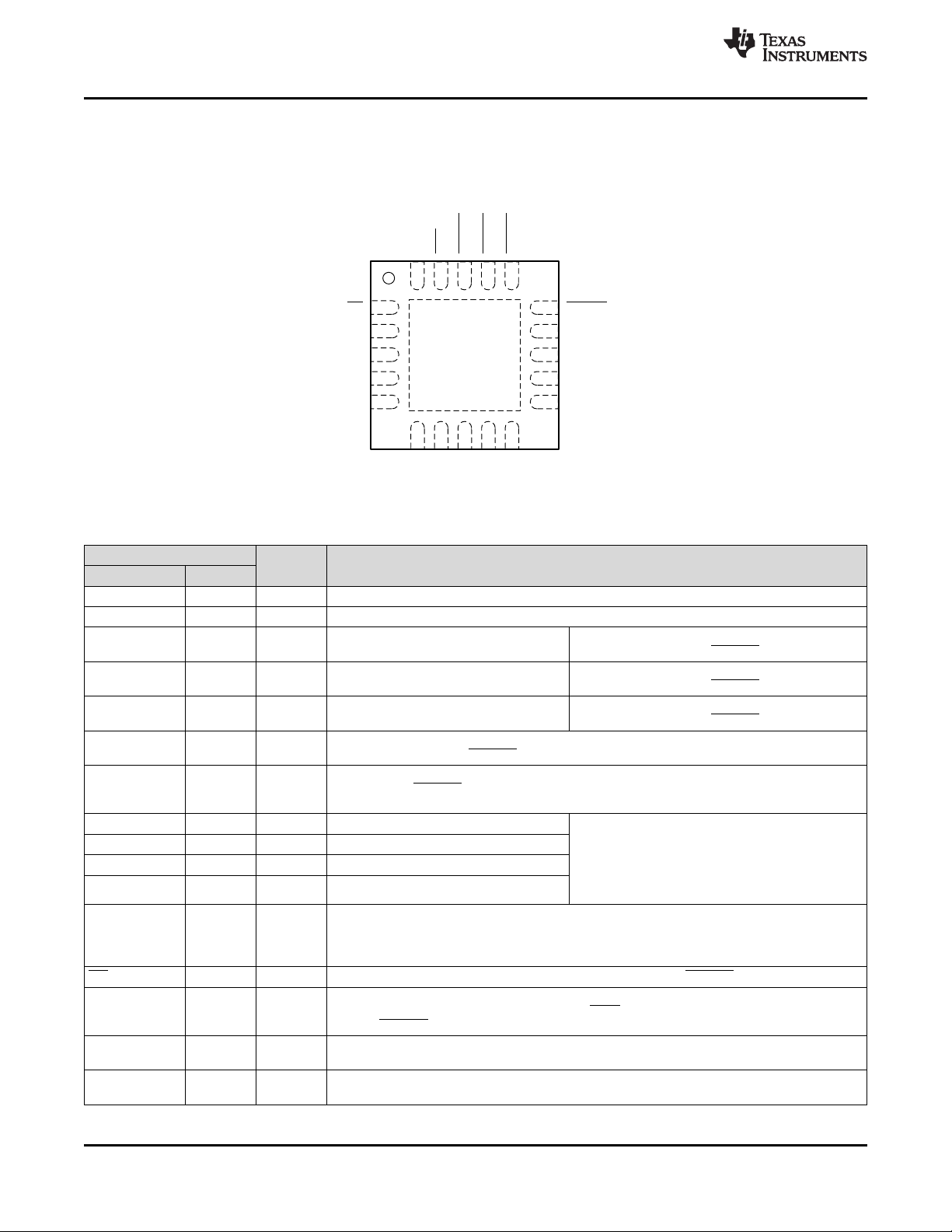
WDI20
RESET317
RESET2
16
RESET418WDO
19
RESET115
V
DD
14
NC
11
GND12
VREF13
MR
1
CT4
2
CT1
5
CT2 4
CT3 3
6
SENSE29SENSE1
10
SENSE3
8
SENSE4L
7
Thermal Pad
TPS386000,TPS386040
SBVS105F –SEPTEMBER 2009–REVISED OCTOBER 2018
5 Pin Configuration and Functions
www.ti.com
RGP Package
20-Pin VQFN
Top View
Pin Functions
PIN
NAME NO.
V
DD
14 I Supply voltage. TI recommends connecting a 0.1-μF ceramic capacitor close to this pin.
GND 12 — Ground
SENSE1 10 I Monitor voltage input to SVS-1
SENSE2 9 I Monitor voltage input to SVS-2
SENSE3 8 I Monitor voltage input to SVS-3
SENSE4L 7 I
SENSE4H 6 I
CT1 5 — Reset delay programming pin for SVS-1 Connecting this pin to VDDthrough a 40-kΩ to
CT2 4 — Reset delay programming pin for SVS-2
CT3 3 — Reset delay programming pin for SVS-3
CT4 2 — Reset delay programming pin for SVS-4
VREF 13 O
MR 1 I Manual reset input for SVS-1. Logic low level of this pin asserts RESET1.
WDI 20 I
NC 11 —
Thermal Pad PAD —
I/O DESCRIPTION
When the voltage at this terminal drops below the
threshold voltage (V
When the voltage at this terminal drops below the
threshold voltage (V
When the voltage at this terminal drops below the
threshold voltage (V
Falling monitor voltage input to SVS-4. When the voltage at this terminal drops below the
threshold voltage (V
), RESET4 is asserted.
ITN
Rising monitor voltage input to SVS-4. When the voltage at this terminal exceeds the threshold
voltage (V
rail in combination with VREF pin. Connect to GND if not being used.
), RESET4 is asserted. This pin can also be used to monitor the negative voltage
ITP
200-kΩ resistor, or leaving it open, selects a fixed
delay time (see the Electrical Characteristics).
Connecting a capacitor > 220 pF between this pin
and GND selects the programmable delay time (see
the Reset Delay Time section).
Reference voltage output. By connecting a resistor network between this pin and the negative
power rail, SENSE4H can monitor the negative power rail. This pin is intended to only source
current into resistor(s). Do not connect resistor(s) to a voltage higher than 1.2 V. Do not connect
only a capacitor.
Watchdog timer (WDT) trigger input. Inputting either a positive or negative logic edge every
610 ms (typical) prevents WDT time out at the WDO or WDO pin. Timer starts from releasing
event of RESET1.
Not internal connection. TI recommends connecting this pin to the GND pin (pin 12), which is
next to this pin.
This pad is the IC substrate. This pad must be connected only to GND or to the floating thermal
pattern on the printed-circuit board (PCB).
), RESET1 is asserted.
ITN
), RESET2 is asserted.
ITN
), RESET3 is asserted.
ITN
4
Submit Documentation Feedback Copyright © 2009–2018, Texas Instruments Incorporated
Product Folder Links: TPS386000 TPS386040
TPS386000,TPS386040
www.ti.com
SBVS105F –SEPTEMBER 2009–REVISED OCTOBER 2018
Pin Functions (continued)
PIN
NAME NO.
TPS386000
RESET1 15 O Active low reset output of SVS-1 RESETn is an open-drain output pin. When
RESET2 16 O Active low reset output of SVS-2
RESET3 17 O Active low reset output of SVS-3
RESET4 18 O Active low reset output of SVS-4
WDO 19 O
TPS386040
RESET1 15 O Active low reset output of SVS-1
RESET2 16 O Active low reset output of SVS-2
RESET3 17 O Active low reset output of SVS-3
RESET4 18 O Active low reset output of SVS-4
WDO 19 O
I/O DESCRIPTION
RESETn is asserted, this pin remains in a lowimpedance state. When RESETn is released, this
pin goes to a high-impedance state after the delay
time programmed by CTn. A pullup resistor to V
or another voltage source is required.
Watchdog timer output. This is an open-drain output pin. When WDT times out, this pin goes to
a low-impedance state to GND. If there is no WDT time-out, this pin stays in a high-impedance
state.
RESETn is a push-pull logic buffer output pin.
When RESETn is asserted, this pin remains logic
low. When RESETn is released, this pin goes to
logic high after the delay time programmed by CTn.
Watchdog timer output. This is a push-pull output pin. When WDT times out, this pin goes to
logic low. If there is no WDT time-out, this pin stays in logic high.
DD
Product Folder Links: TPS386000 TPS386040
Submit Documentation FeedbackCopyright © 2009–2018, Texas Instruments Incorporated
5
TPS386000,TPS386040
SBVS105F –SEPTEMBER 2009–REVISED OCTOBER 2018
www.ti.com
6 Specifications
6.1 Absolute Maximum Ratings
SENSE1
(1)
, V
SENSE2
MIN MAX UNIT
–0.3 7
–0.3 VDD+ 0.3
,
–0.3 7
V
–40 150
–40 125
°COperating ambient, T
–65 150
VALUE UNIT
(1)
±2000
±500
V
Over operating junction temperature range, unless otherwise noted.
Input, V
DD
Voltage
CT pin, V
V
RESET1
V
SENSE3
CT1
, V
, V
, V
CT2
RESET2
SENSE4L
, V
, V
, V
, V
CT3
RESET3
SENSE4H
CT4
, V
RESET4
, V
WDI
, VMR, V
, V
WDO
Current RESETn , RESETn, WDO, WDO, VREF pin 5 mA
Power dissipation Continuous total See Thermal Information table
(2)
J
A
Temperature
Operating virtual junction, T
Storage, T
stg
(1) Stresses beyond those listed under Absolute Maximum Ratings may cause permanent damage to the device. These are stress ratings
only, which do not imply functional operation of the device at these or any other conditions beyond those indicated under Recommended
Operating Conditions. Exposure to absolute-maximum-rated conditions for extended periods may affect device reliability.
(2) As a result of the low dissipated power in this device, it is assumed that TJ= TA.
6.2 ESD Ratings
Human-body model (HBM), per ANSI/ESDA/JEDEC JS-001
V
(ESD)
(1) JEDEC document JEP155 states that 500-V HBM allows safe manufacturing with a standard ESD control process.
(2) JEDEC document JEP157 states that 250-V CDM allows safe manufacturing with a standard ESD control process.
Electrostatic discharge
Charged-device model (CDM), per JEDEC specification JESD22-
(2)
C101
6.3 Recommended Operating Conditions
Over operating junction temperature range (unless otherwise noted).
MIN NOM MAX UNIT
V
DD
(1)
V
SENSE
WDI
(HI)
WDI
(LO)
V
MR
CTn 0.22 1000 nF
R
PULL-UP
T
J
(1) All sense inputs.
1.8 6.5 V
0 V
0.7V
DD
0 0.3V
0 V
DD
V
DD
DD
DD
6.5 100 10000 kΩ
–40 25 125 °C
V
V
V
V
6.4 Thermal Information
TPS3860x0
THERMAL METRIC
R
θJA
R
θJC(top)
R
θJB
ψ
JT
ψ
JB
R
θJC(bot)
Junction-to-ambient thermal resistance 46 °C/W
Junction-to-case (top) thermal resistance 52.8 °C/W
Junction-to-board thermal resistance 22.4 °C/W
Junction-to-top characterization parameter 1.3 °C/W
Junction-to-board characterization parameter 22.4 °C/W
Junction-to-case (bottom) thermal resistance 4.3 °C/W
(1) For more information about traditional and new thermal metrics, see the Semiconductor and IC Package Thermal Metrics application
report (SPRA953).
6
Submit Documentation Feedback Copyright © 2009–2018, Texas Instruments Incorporated
Product Folder Links: TPS386000 TPS386040
(1)
UNITRGP (VQFN)
20 PINS
TPS386000,TPS386040
www.ti.com
SBVS105F –SEPTEMBER 2009–REVISED OCTOBER 2018
6.5 Electrical Characteristics
Over the operating temperature range of TJ= –40°C to 125°C, 1.8 V < VDD< 6.5 V, R
(TPS386000 only), C
(n = 1, 2, 3, 4L, 4H) = 50 pF to GND, R
RESETn
= 100 kΩ to VDD, C
WDO
to VDD, WDI = GND, and CTn (n = 1, 2, 3, 4) = open, unless otherwise noted. Typical values are at TJ= 25°C.
PARAMETER TEST CONDITIONS MIN TYP MAX UNIT
V
DD
I
DD
V
ITN
V
ITP
V
HYSN
V
HYSP
I
SENSE
I
CT
V
TH(CTn)
V
IL
V
IH
V
OL
V
OH
I
LKG
V
REF
C
IN
(1) Toggling WDI for a period less than t
(2) These specifications are beyond the recommended VDDrange, and only define RESETn or RESETn output performance during V
(3) The lowest supply voltage (VDD) at which RESETn or RESETn becomes active; t
(4) CTn (where n = 1, 2, 3, or 4) are constant current charging sources working from a range of 0 V to V
Input supply range 1.8 6.5 V
Supply current (current into VDDpin)
VDD= 3.3 V, RESETn or RESETn not
asserted, WDI toggling
and VREF open
VDD= 6.5 V, RESETn or RESETn not
asserted, WDI toggling
(1)
, no output load,
(1)
, no output load,
and VREF open
Power-up reset voltage
(2)(3)
VOL(max) = 0.2 V, I
= 15 μA 0.9 V
RESETn
Negative-going input threshold voltage SENSE1, SENSE2, SENSE3, SENSE4L 396 400 404 mV
Positive-going input threshold voltage SENSE4H 396 400 404 mV
Hysteresis (positive-going) on V
ITN
Hysteresis (negative-going) on V
Input current at SENSEm pin V
CTn pin charging
current
CT1 C
CT2, CT3, CT4 C
CTn pin threshold C
SENSE1, SENSE2, SENSE3, SENSE4L 3.5 10 mV
SENSE4H 3.5 10 mV
ITP
= 0.42 V –25 ±1 +25 nA
SENSEm
> 220 pF, V
CT1
> 220 pF, V
CTn
> 220 pF 1.18 1.238 1.299 V
CTn
CT1
CTn
= 0.5 V
= 0.5 V
(4)
(4)
MR and WDI logic low input 0 0.3V
MR and WDI logic high input 0.7V
Low-level RESETn or RESETn output
voltage
IOL= 1 mA 0.4 V
SENSEn = 0 V, 1.3 V < VDD< 1.8 V,
IOL= 0.4 mA
(2)
Low-level WDO output voltage IOL= 1 mA 0.4
High-level RESETn
or RESETn output
voltage
High-level WDO
output voltage
RESETn, RESETn,
WDO, and WDO
leakage current
Reference voltage output
TPS386040
only
TPS386040
only
TPS386000
only
IOL= –1 mA VDD– 0.4 V
IOL= –1 mA VDD– 0.4
SENSEn = 0 V, 1.3 V < VDD< 1.8 V,
IOL= –0.4 mA
V
RESETn
and WDO are logic high
1 μA < I
sink)
(2)
= 6.5 V, RESETn, RESETn, WDO,
< 0.2 mA (source only, no
VREF
Input pin capacitance CTn: 0 V to VDD, other pins: 0 V to 6.5 V 5 pF
negatively affects IDD.
WDT
ramp up.
RISE(VDD)
V
= 0.5 V. For ICTperformance between 0 V and V
CTn
, see Figure 28.
TH(CTn)
(n = 1, 2, 3, 4) = 100 kΩ to V
RESETn
= 50 pF to GND, VMR= 100 kΩ
WDO
11 19
13 22
245 300 355
235 300 365
DD
VDD– 0.3
–300 300 nA
1.18 1.2 1.22 V
≥ 15 μs/V.
, and the device is tested at
TH(CTn)
DD
0.3
DD
μA
nA
V
V
V
V
DD
Product Folder Links: TPS386000 TPS386040
Submit Documentation FeedbackCopyright © 2009–2018, Texas Instruments Incorporated
7
V
DD
SENSE1
V
IT–
t
d
t
d
V
hys–
0.9 V
MR
RESET1
t
t
t
t
TPS386000,TPS386040
SBVS105F –SEPTEMBER 2009–REVISED OCTOBER 2018
6.6 Timing Requirements
Over the operating temperature range of TJ= –40°C to 125°C, 1.8 V < VDD< 6.5 V, R
(TPS386000 only), C
(n = 1, 2, 3, 4L, 4H) = 50 pF to GND, R
RESETn
= 100 kΩ to VDD, C
WDO
to VDD, WDI = GND, and CTn (n = 1, 2, 3, 4) = open, unless otherwise noted. Nominal values are at TJ= 25°C.
MIN TYP MAX UNIT
t
W
Input pulse width to
SENSEm and MR pins
SENSEm: 1.05 V
0.95 V
→ 1.05 V
ITP
MR: 0.7 VDD→ 0.3 V
→ 0.95 V
ITN
ITP
DD
ITN
or
(n = 1, 2, 3, 4) = 100 kΩ to V
RESETn
= 50 pF to GND, VMR= 100 kΩ
WDO
4 μs
1 ns
6.7 Switching Characteristics
Over the operating temperature range of TJ= –40°C to 125°C, 1.8 V < VDD< 6.5 V, R
(TPS386000 only), C
(n = 1, 2, 3, 4L, 4H) = 50 pF to GND, R
RESETn
= 100 kΩ to VDD, C
WDO
to VDD, WDI = GND, and CTn (n = 1, 2, 3, 4) = open, unless otherwise noted. Typical values are at TJ= 25°C.
PARAMETER TEST CONDITIONS MIN TYP MAX UNIT
t
D
t
WDT
RESETn or RESETn
delay time
Watchdog timer time-out period
(1) Start from RESET1 or RESET1 release or last WDI transition.
CTn = Open 14 20 24
CTn = V
(1)
DD
225 300 375
450 600 750 ms
(n = 1, 2, 3, 4) = 100 kΩ to V
RESETn
= 50 pF to GND, VMR= 100 kΩ
WDO
www.ti.com
DD
DD
ms
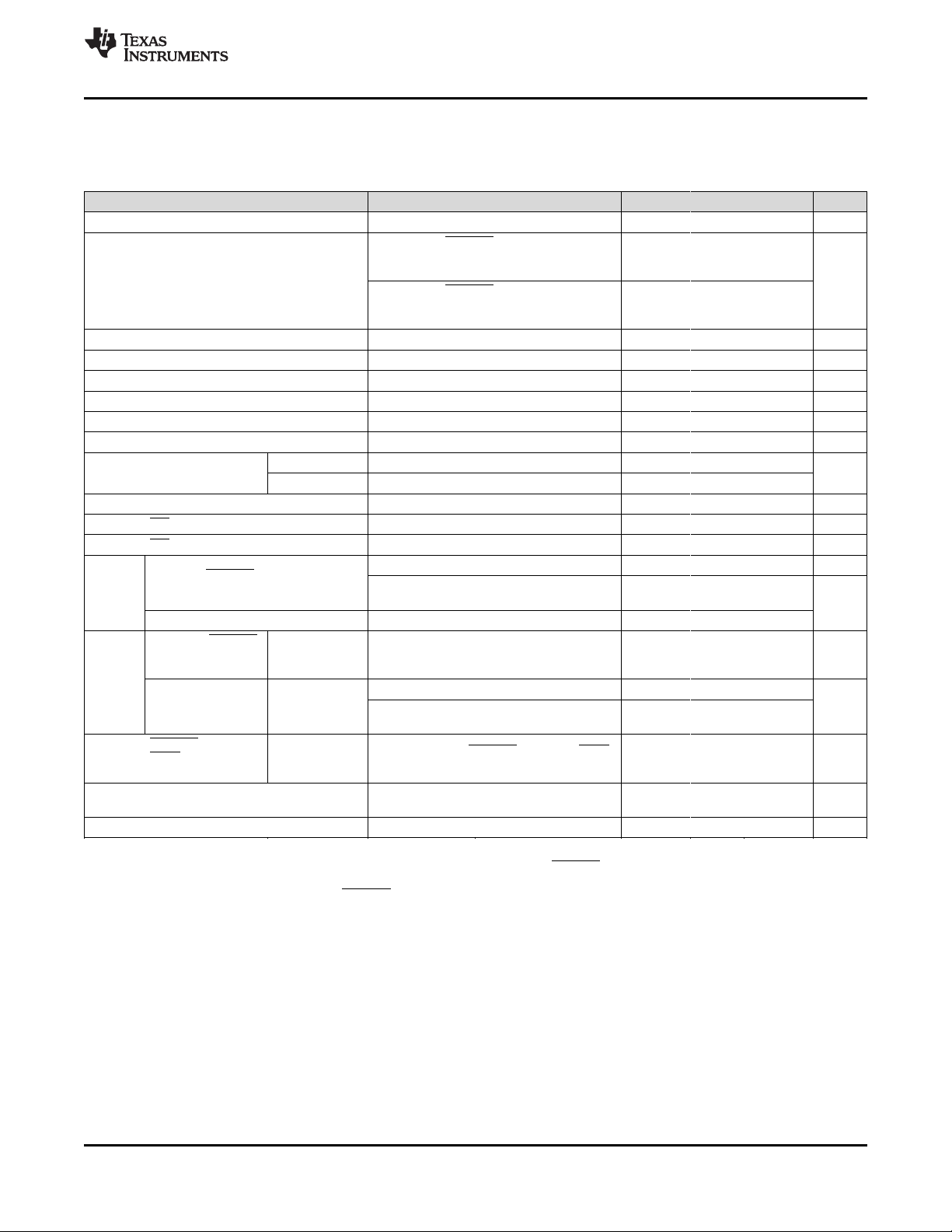
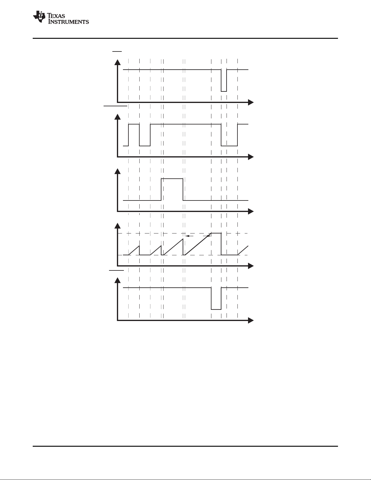
Figure 1. SVS-1 Timing Diagram
8
Submit Documentation Feedback Copyright © 2009–2018, Texas Instruments Incorporated
Product Folder Links: TPS386000 TPS386040
V
DD
SENSE3
V
IT–
V
hys–
0.9 V
RESET3
t
t
t
t
d
t
d
V
CC
SENSE2
V
IT–
V
hys–
0.9 V
RESET2
t
t
t
t
d
www.ti.com
TPS386000,TPS386040
SBVS105F –SEPTEMBER 2009–REVISED OCTOBER 2018
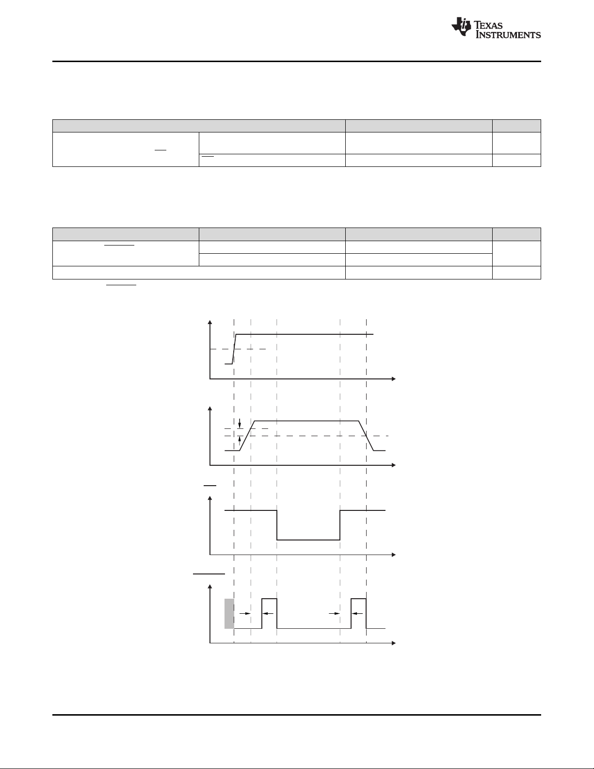
Figure 2. SVS-2 Timing Diagram
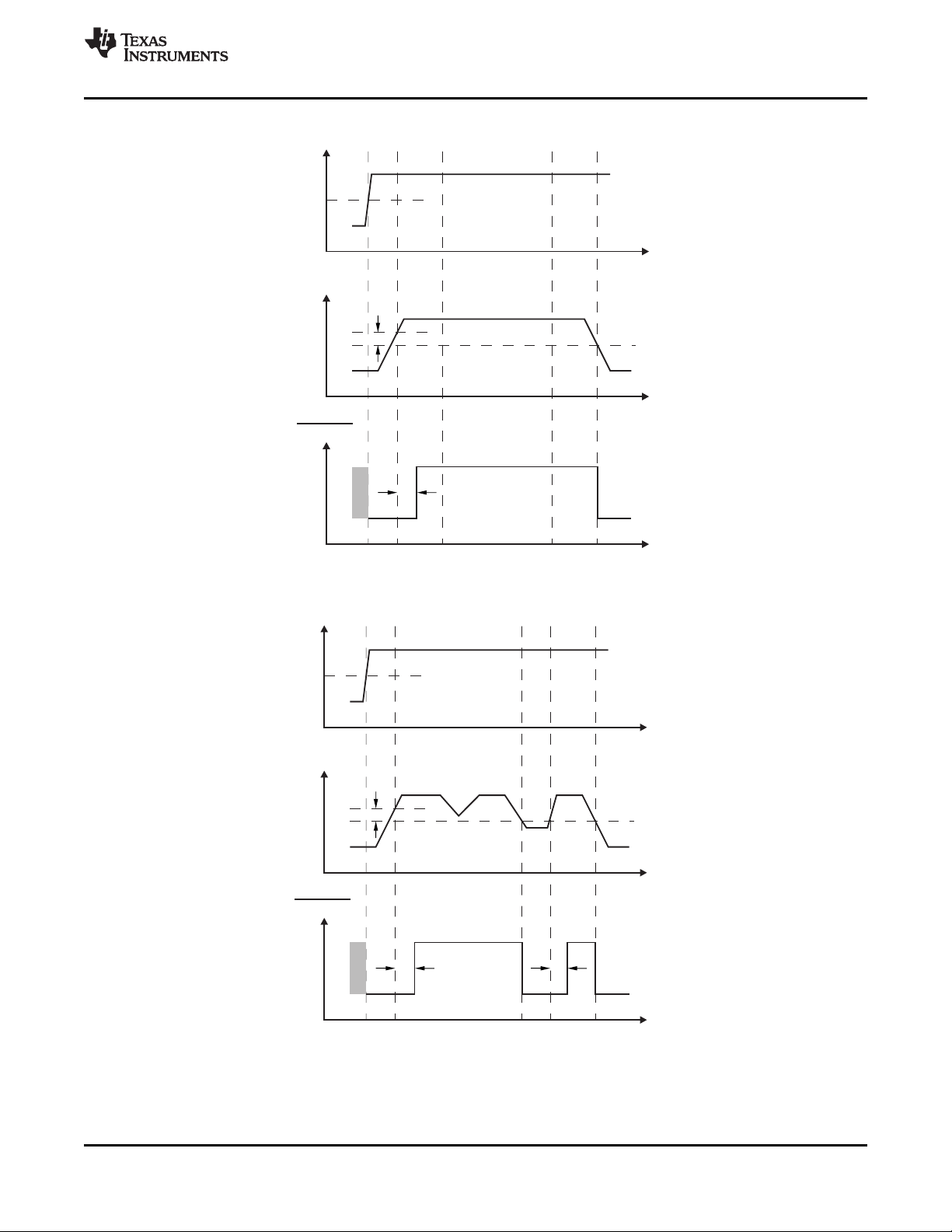
Figure 3. SVS-3 Timing Diagram
Submit Documentation FeedbackCopyright © 2009–2018, Texas Instruments Incorporated
Product Folder Links: TPS386000 TPS386040
9
V
DD
SENSE4L
SENSE4H
V
IT–
V
IT+
V
HYS+
V
HYS–
0.9 V
RESET4
t
t
t
t
t
D
TPS386000,TPS386040
SBVS105F –SEPTEMBER 2009–REVISED OCTOBER 2018
www.ti.com
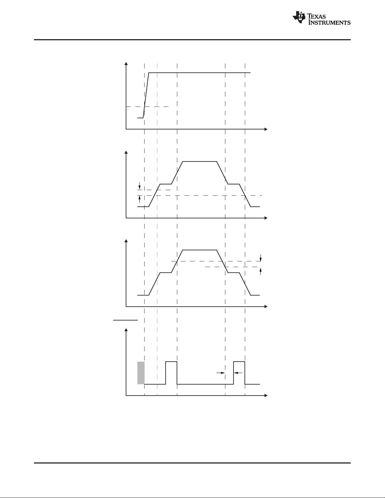
Figure 4. SVS-4 Timing Diagram
10
Submit Documentation Feedback Copyright © 2009–2018, Texas Instruments Incorporated
Product Folder Links: TPS386000 TPS386040
WDI
Zero
Timeout
WDO
RESET1
t
t
t
t
MR
t
t
WDT
(Internaltimer)
www.ti.com
TPS386000,TPS386040
SBVS105F –SEPTEMBER 2009–REVISED OCTOBER 2018
Figure 5. WDT Timing Diagram
Product Folder Links: TPS386000 TPS386040
Submit Documentation FeedbackCopyright © 2009–2018, Texas Instruments Incorporated
11
RESET1
t
t
t
(Internaltimer)
MR = WDO
t
WDT
Event1 Event2 Event3
WDI
t
TPS386000,TPS386040
SBVS105F –SEPTEMBER 2009–REVISED OCTOBER 2018
www.ti.com
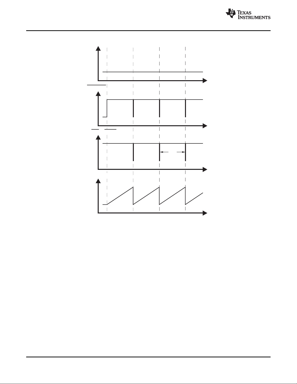
Figure 6. Legacy WDT Configuration Timing Diagram
12
Submit Documentation Feedback Copyright © 2009–2018, Texas Instruments Incorporated
Product Folder Links: TPS386000 TPS386040
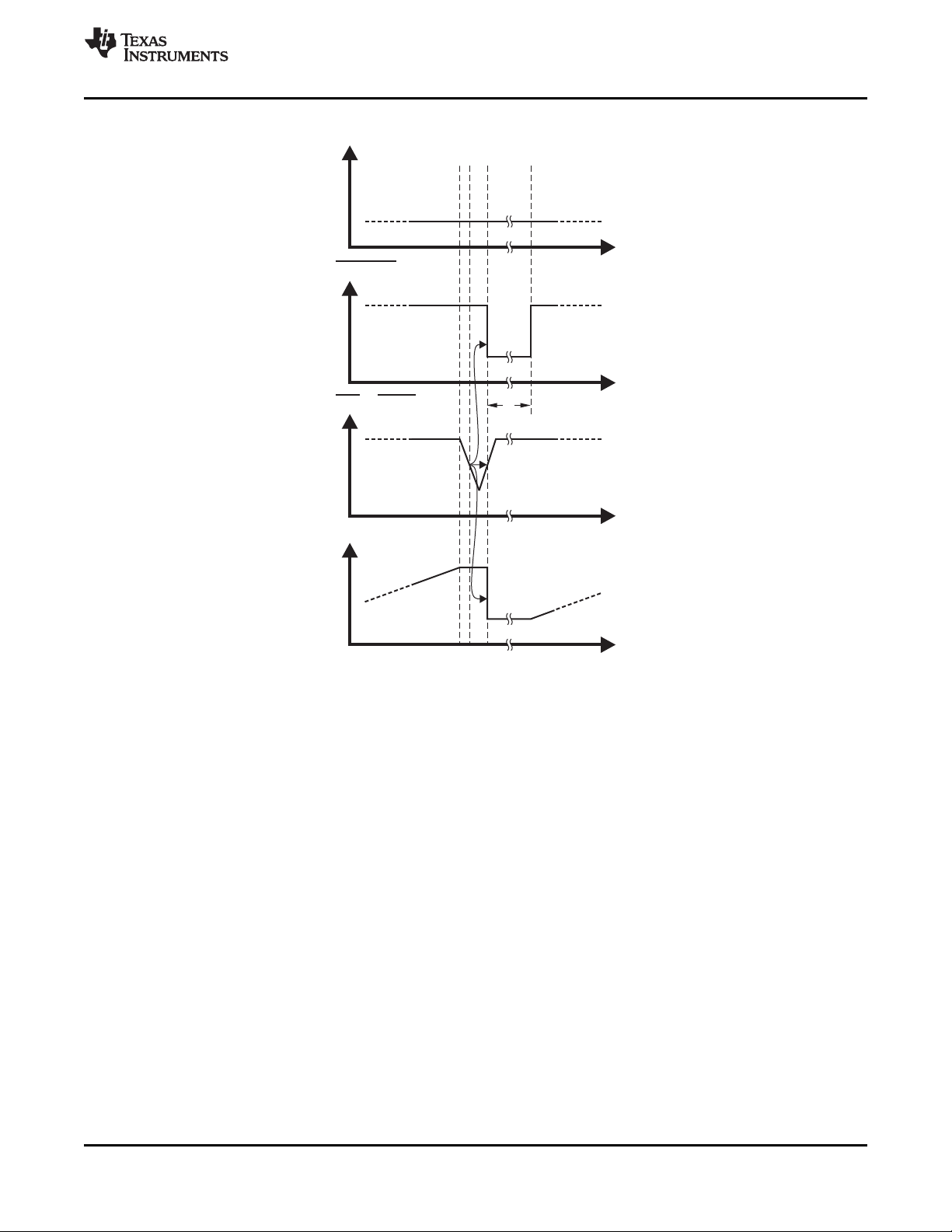
Event1
RESET1
(Internaltimer)
MR = WDO
t
D
WDI
www.ti.com
TPS386000,TPS386040
SBVS105F –SEPTEMBER 2009–REVISED OCTOBER 2018
Figure 7. Enlarged View of Event 1 from Figure 6
Product Folder Links: TPS386000 TPS386040
Submit Documentation FeedbackCopyright © 2009–2018, Texas Instruments Incorporated
13

-50 -30 -10 10 30 50 70 90 110 130
Temperature(°C)
550
500
450
400
350
300
250
RESETn Delay(ms)
CT1
CT2
CT3 CT4
NOTE:Thesecurvescontainvarianceofcapacitorvalues.
-50 -30 -10 10 30 50 70 90 110 130
Temperature (°C)
700
680
660
640
620
600
580
560
540
520
500
WDO Delay (ms)
V = 1.8 V
DD
V = 3.3 V
DD
V = 6.5 V
DD
-50 -30 -10 10 30 50 70 90 110 130
Temperature(°C)
25
20
15
10
5
0
RESETn
Delay(ms)
CT1
CT3
CT2 CT4
-50 -30 -10 10 30 50 70 90 110 130
Temperature(°C)
360
340
320
300
280
260
240
RESETn Delay(ms)
CT2 CT4
CT1
CT3
10 5 6 7432
V (V)
20
18
16
14
12
10
8
6
4
2
0
I ( A)m
DD
0 C°
- °40 C
+25 C°
+85 C°
NOTE: UVLO released at approximately 1.5V.
+105 C°
+125 C°
0.0001 0.001 0.01 0.1 1
CTn ( F)m
10000
1000
100
10
1
RESETn
Delay (ms)
- °40 C
+85 C°
+125 C°
0 C°
+25 C°
TPS386000,TPS386040
SBVS105F –SEPTEMBER 2009–REVISED OCTOBER 2018
www.ti.com
6.8 Typical Characteristics
At TA= 25°C, and VDD= 3.3 V, with both options (TPS386000 and TPS386040) having the same characteristics, unless
otherwise noted.
Figure 8. TPS386040 Supply Current vs Supply Voltage Figure 9. TPS386040 RESETn Time-out Period vs CTn
Figure 10. TPS386040 (CTn = Open) RESETn Time-out
Period vs Temperature
14
Figure 12. TPS386040 (CTn = 0.1 µF) RESETn Time-out
Submit Documentation Feedback Copyright © 2009–2018, Texas Instruments Incorporated
Period vs Temperature
Figure 11. TPS386040 (CTn = VDD) RESETn Time-out Period
vs Temperature
Figure 13. TPS386040 WDO Time-out Period vs Temperature
Product Folder Links: TPS386000 TPS386040

-50 -30 -10 10 30 50 70 90 110 130
Temperature (°C)
408
406
404
402
400
398
396
V , (V + V
ITN ITN HYSN
) (mV)
V + V , V =
ITN HYSN DD
6.5 V
V + V , V =
ITN HYSN DD
1.8 V
V , V =
ITN DD
3.3 V
V , V =
ITN DD
6.5 V
V , V =
ITN DD
1.8 V
V + V , V =
ITN HYSN DD
3.3 V
-50 -30 -10 10 30 50 70 90 110 130
Temperature (°C)
404
402
400
398
396
394
392
V , (V + V
ITP ITP HYSP
) (mV)
V + V , V =
ITP HYSP DD
6.5 V
V + V , V =
ITP HYSP DD
1.8 V
V , V =
ITP DD
6.5 V
V , V = 3
ITP DD
.3 V
V , V =
ITP DD
1.8 V
V + V , V =
ITP HYSP DD
3.3 V
-50 -30 -10 10 30 50 70 90 110 130
Temperature (°C)
408
406
404
402
400
398
396
V , (V + V
ITN ITN HYSN
) (mV)
V + V , V
ITN HYSN DD
= 6.5 V
V + V , V =
ITN HYSN DD
1.8 V
V + V , V =
ITN HYSN DD
3.3 V
V , V =
ITN DD
6.5 V
V , V =
ITN DD
1.8 V
V , V =
ITN DD
3.3 V
-50 -30 -10 10 30 50 70 90 110 130
Temperature (°C)
408
406
404
402
400
398
396
V , (V + V
ITN ITN HYSN
) (mV)
V + V , V =
ITN HYSN DD
6.5 V
V + V , V =
ITN HYSN DD
1.8 V
V + V , V =
ITN HYSN DD
3.3 V
V , V =
ITN DD
1.8 V
V , V =
ITN DD
6.5 V
V , V =
ITN DD
3.3 V
0.1 1 10 100
Overdrive (%)
100
10
1
0.1
SENSEn Pulse Width ( s)m
SENSE4H
SENSE3
SENSE4L
SENSE1
SENSE2
-50 -30 -10 10 30 50 70 90 110 130
Temperature (°C)
408
406
404
402
400
398
396
V , (V + V
ITN ITN HYSN
) (mV)
V + V , V
ITN HYSN DD
= 6.5 V
V + V , V =
ITN HYSN DD
1.8 V
V + V , V =
ITN HYSN DD
3.3 V
V , V = 6.5 V
ITN DD
V , V =
ITN DD
3.3 V
V , V =
ITN DD
1.8 V
TPS386000,TPS386040
www.ti.com
SBVS105F –SEPTEMBER 2009–REVISED OCTOBER 2018
Typical Characteristics (continued)
At TA= 25°C, and VDD= 3.3 V, with both options (TPS386000 and TPS386040) having the same characteristics, unless
otherwise noted.
See Figure 29 for measurement technique
Figure 14. TPS386040 SENSEn Minimum Pulse Width
vs SENSEn Threshold Overdrive Voltage
Figure 16. TPS386040 SENSE2 Threshold Voltage vs
Temperature
Figure 15. TPS386040 SENSE1 Threshold Voltage vs
Temperature
Figure 17. TPS386040 SENSE3 Threshold Voltage vs
Temperature
Figure 18. TPS386040 SENSE4L Threshold Voltage vs
Temperature
Product Folder Links: TPS386000 TPS386040
Figure 19. TPS386040 SENSE4H Threshold Voltage vs
Temperature
Submit Documentation FeedbackCopyright © 2009–2018, Texas Instruments Incorporated
15

0 50 100 150 200 250 300 350 400
Load ( A)μ
1.200
1.198
1.196
1.194
1.192
1.190
1.188
V (V)
REF
0 C°
- °40 C
25 C°
85 C°
125 C°
105 C°
0 50 100 150 200 250 300 350 400
Load ( A)μ
1.200
1.198
1.196
1.194
1.192
1.190
1.188
V (V)
REF
0 C°
40 C°
25 C°
85 C°
125 C°
105 C°
0 0.1 0.2 0.3 0.4 0.5 0.6 0.7 0.8 0.9 1.0
Output Source Current (mA)
0
-0.050
-0.100
-0.150
-0.200
-0.250
V - V (V)
DD OH
V = 1.8 V, 25°C
DD
V = 3.3 V, 25°C
DD
V = 6.5 V, 25°C
DD
-50 -30 -10 10 30 50 70 90 110 130
Temperature ( C)°
0
-0.05
-0.10
-0.15
-0.20
-0.25
V - V (V)
DD OH
V = 1.8 V
DD
V = 6.5 V
DD
V = 3.3 V
DD
0 0.1 0.2 0.3 0.4 0.5 0.6 0.7 0.8 0.9 1.0
Output Sink Current (mA)
0.200
0.180
0.160
0.140
0.120
0.100
0.080
0.060
0.040
0.020
0
Low-Level Output Voltage (V)
V = 6.5 V, 25°C
DD
V = 1.8 V, 25°C
DD
V = 3.3 V, 25°C
DD
-50 -30 -10 10 30 50 70 90 110 130
Temperature (°C)
0.200
0.180
0.160
0.140
0.120
0.100
0.080
0.060
0.040
0.020
0
Low-Level Output Voltage (V)
V = 1.8 V
DD
V = 6.5 V
DD
V = 3.3 V
DD
TPS386000,TPS386040
SBVS105F –SEPTEMBER 2009–REVISED OCTOBER 2018
www.ti.com
Typical Characteristics (continued)
At TA= 25°C, and VDD= 3.3 V, with both options (TPS386000 and TPS386040) having the same characteristics, unless
otherwise noted.
Figure 20. Output Voltage Low vs Output Current Figure 21. Output Voltage Low at 1 mA vs Temperature
Figure 22. Output Voltage High vs Output Current Figure 23. Output Voltage High at 1 mA vs Temperature
16
Figure 24. TPS386040 V
Submit Documentation Feedback Copyright © 2009–2018, Texas Instruments Incorporated
Output Load Regulation
REF
(VDD= 1.8 V)
Figure 25. TPS386040 V
Product Folder Links: TPS386000 TPS386040
Output Load Regulation
REF
(VDD= 3.3 V)

-50 -30 -10 10 30 50 70 90 110 130
Temperature ( C)°
0.33
0.32
0.31
0.30
0.29
0.28
0.27
Current ( A)μ
0 V
0.1 V
0.3 V
0.5 V
1.1 V
0.7 V
0.9 V
-50 -30 -10 10 30 50 70 90 110 130
Temperature (°C)
1.207
1.205
1.203
1.201
1.199
1.197
1.195
Reference Voltage (V)
V = 6.5 V
DD
V = 3.3 V
DD
V = 1.8 V
DD
0 50 100 150 200 250 300 350 400
Load ( A)μ
1.207
1.205
1.203
1.201
1.199
1.197
1.195
V (V)
REF
0 C°
- °40 C
25 C°
85 C°
125 C°
105 C°
TPS386000,TPS386040
www.ti.com
SBVS105F –SEPTEMBER 2009–REVISED OCTOBER 2018
Typical Characteristics (continued)
At TA= 25°C, and VDD= 3.3 V, with both options (TPS386000 and TPS386040) having the same characteristics, unless
otherwise noted.
Figure 26. TPS386040 V
(VDD= 6.5 V)
Figure 28. TPS386040 CT1 to CT4 Pin Charging Current vs Temperature Over CT Pin Voltage
Output Load Regulation
REF
Figure 27. TPS386040 V
at 0 µA vs Temperature
REF
Product Folder Links: TPS386000 TPS386040
Submit Documentation FeedbackCopyright © 2009–2018, Texas Instruments Incorporated
17

SENSEnVoltage(V)
Time
V =0.4V
ITN
Y
1
Y
2
Z
1
Z
2
X1=
Z
1
0.4
´ 100(%)
X2=
Z
2
0.4
´ 100(%)
X andX areoverdrive(%)valuescalculated
fromactualSENSEnvoltageamplitudes
measuredasZ andZ .
1 2
1 2
Y istheminimumpulsewidththatgives
RESETnor transition.
GreaterZ producesshorterY .
ForSENSE4H,thisgraphshouldbeinverted
180degreesonthevoltageaxis.
N
N N
RESETn
V =0.42V
ITN
TPS386000,TPS386040
SBVS105F –SEPTEMBER 2009–REVISED OCTOBER 2018
7 Parameter Measurement Information
Figure 29. Overdrive Measurement Method
www.ti.com
18
Submit Documentation Feedback Copyright © 2009–2018, Texas Instruments Incorporated
Product Folder Links: TPS386000 TPS386040

TPS386000,TPS386040
www.ti.com
SBVS105F –SEPTEMBER 2009–REVISED OCTOBER 2018
8 Detailed Description
8.1 Overview
The TPS3860x0 multi-channel supervisory family of devices combines four complete SVS function sets into one
IC, along with a watchdog timer, a window comparator, and negative voltage sensing. The design of each SVS
channel is based on the single-channel supervisory device series, TPS3808. The TPS3860x0 is designed to
assert RESETn or RESETn signals, as shown in Table 1, Table 2, Table 3, and Table 4. The RESETn or
RESETn outputs remain asserted during a user-configurable delay time after the event of reset release (see the
Reset Delay Time section).
The TPS3860x0 has a very low quiescent current of 11 μA (typical) and is available in a small, 4-mm × 4-mm,
20-Pin VQFN package.
Product Folder Links: TPS386000 TPS386040
Submit Documentation FeedbackCopyright © 2009–2018, Texas Instruments Incorporated
19

WDT
VREF
WDI
RESET4
RESET3
RESET2
RESET1
WDO
VREF
VDD
GND
MR
SENSE1
CT1
SENSE3
SENSE2
CT3
CT2
SENSE4L
SENSE4H
CT4
0.4V
0.4V
0.4V
0.4V
Delay
Delay
Delay
Delay
TPS386000,TPS386040
SBVS105F –SEPTEMBER 2009–REVISED OCTOBER 2018
8.2 Functional Block Diagrams
www.ti.com
Figure 30. TPS386000 Block Diagram
20
Submit Documentation Feedback Copyright © 2009–2018, Texas Instruments Incorporated
Product Folder Links: TPS386000 TPS386040

WDT
WDI
RESET4
RESET3
RESET2
RESET1
WDO
VREF
MR
SENSE1
CT1
SENSE3
SENSE2
CT3
CT2
SENSE4L
SENSE4H
CT4
V
DD
GND
VREF
Delay
Delay
Delay
Delay
0.4V
0.4V
0.4V
0.4V
www.ti.com
Functional Block Diagrams (continued)
TPS386000,TPS386040
SBVS105F –SEPTEMBER 2009–REVISED OCTOBER 2018
Figure 31. TPS386040 Block Diagram
Product Folder Links: TPS386000 TPS386040
Submit Documentation FeedbackCopyright © 2009–2018, Texas Instruments Incorporated
21

TPS386000,TPS386040
SBVS105F –SEPTEMBER 2009–REVISED OCTOBER 2018
www.ti.com
8.3 Feature Description
8.3.1 Voltage Monitoring
Each SENSEm (m = 1, 2, 3, 4L) pin can be set to monitor any voltage threshold above 0.4 V using an external
resistor divider. The SENSE4H pin can be used for any overvoltage detection greater than 0.4 V, or for negative
voltage detection using an external resistor divider (see the Sensing a Negative Voltage section). A broad range
of voltage threshold and reset delay time adjustments can be supported, allowing these devices to be used in a
wide array of applications.
The TPS3860x0 is relatively immune to short negative transients on the SENSEn pin. Sensitivity to transients
depends on threshold overdrive, as shown in (Figure 14).
8.3.2 Manual Reset
The manual reset (MR) input allows external logic signal from other processors, logic circuits, and/or discrete
sensors to initiate a device reset. Because MR is connected to SVS-1, the RESET1 or RESET1 pin is intended
to be connected to processor(s) as a primary reset source. A logic low at MR causes RESET1 or RESET1 to
assert. After MR returns to a logic high and SENSE1 is above its reset threshold, RESET1 or RESET1 is
released after the user-configured reset delay time. Unlike the TPS3808 series, the TPS3860x0 does not
integrate an internal pullup resistor between MR and VDD.
To control the MR function from more than one logic signal, the logic signals can be combined by wired-OR into
the MR pin using multiple NMOS transistors and one pullup resistor.
8.3.3 Watchdog Timer
The TPS3860x0 provides a watchdog timer with a dedicated watchdog error output, WDO or WDO. The WDO or
WDO output enables application board designers to easily detect and resolve the hang-up status of a processor.
As with MR, the watchdog timer function of the device is also tied to SVS-1. Figure 5 shows the timing diagram
of the WDT function. Once RESET1 or RESET1 is released, the internal watchdog timer starts its countdown.
Inputting a logic level transition at WDI resets the internal timer count and the timer restarts the countdown. If the
TPS3860x0 fails to receive any WDI rising or falling edge within the WDT period, the WDT times out and asserts
WDO or WDO. After WDO or WDO is asserted, the device holds the status with the internal latch circuit. To clear
this time-out status, a reset assertion of RESET1 or RESET is required. That is, a negative pulse to MR, a
SENSE1 voltage less than V
To reset the processor by WDT time-out, WDO can be combined with RESET1 by using the wired-OR with the
TPS386000 option.
For legacy applications where the watchdog timer time-out causes RESET1 to assert, connect WDO to MR; see
Figure 35 for the connections and see Figure 6 and Figure 7 for the timing diagrams.
, or a VDDpower down is required.
ITN
22
Submit Documentation Feedback Copyright © 2009–2018, Texas Instruments Incorporated
Product Folder Links: TPS386000 TPS386040

TPS386000,TPS386040
www.ti.com
SBVS105F –SEPTEMBER 2009–REVISED OCTOBER 2018
Feature Description (continued)
8.3.4 Reset Output
In a typical TPS3860x0 application, RESETn or RESETn outputs are connected to the reset input of a processor
(DSP, CPU, FPGA, ASIC, and so forth), or connected to the enable input of a voltage regulator (DC-DC, LDO,
and so forth).
The TPS386000 provides open-drain reset outputs. Pullup resistors must be used to hold these lines high when
RESETn is not asserted, or when RESETn is asserted. By connecting pullup resistors to the proper voltage rails
(up to 6.5 V), RESETn or RESETn output nodes can be connected to the other devices at the correct interface
voltage levels. The pullup resistor should be no smaller than 10 kΩ to ensure the safe operation of the output
transistors. By using wired-OR logic, any combination of RESETn can be merged into one logic signal.
The TPS386040 provides pushpull reset outputs. The logic high level of the outputs is determined by the V
voltage. With this configuration, pullup resistors are not required and some board area can be saved. However,
all the interface logic levels should be examined. All RESETn or RESETn connections must be compatible with
the VDDlogic level.
The RESETn or RESETn outputs are defined for VDDvoltage higher than 0.9 V. To ensure that the target
processor(s) are properly reset, the VDDsupply input should be fed by the available power rail as early as
possible in application circuits. Table 1, Table 2, Table 3, and Table 4 are truth tables that describe how the
outputs are asserted or released. Figure 1, Figure 2, Figure 3, and Figure 4 show the SVS-n timing diagrams.
When the conditions are met, the device changes the state of SVS-n from asserted to released after a userconfigurable delay time. However, the transitions from released-state to asserted-state are performed almost
immediately with minimal propagation delay. Figure 3 describes the relationship between threshold voltages (V
and V
) and SENSEm voltage; and all SVS-1, SVS-2, SVS-3, and SVS-4 have the same behavior of
HYSN
Figure 3.
DD
ITN
8.4 Device Functional Modes
The following tables show the state of the output and the status of the part under various conditions.
Table 1. SVS-1 Truth Table
CONDITION OUTPUT STATUS
MR = Low SENSE1 < V
MR = Low SENSE1 > V
MR = High SENSE1 < V
MR = High SENSE1 > V
ITN
ITN
ITN
ITN
Table 2. SVS-2 Truth Table
CONDITION OUTPUT STATUS
SENSE2 < V
SENSE2 > V
ITN
ITN
RESET2 = Low Reset asserted
RESET2 = High Reset released after delay
Table 3. SVS-3 Truth Table
CONDITION OUTPUT STATUS
SENSE3 < V
SENSE3 > V
ITN
ITN
RESET3 = Low Reset asserted
RESET3 = High Reset released after delay
RESET1 = Low Reset asserted
RESET1 = Low Reset asserted
RESET1 = Low Reset asserted
RESET1 = High
Reset released after
delay
Product Folder Links: TPS386000 TPS386040
Submit Documentation FeedbackCopyright © 2009–2018, Texas Instruments Incorporated
23

TPS386000,TPS386040
SBVS105F –SEPTEMBER 2009–REVISED OCTOBER 2018
Table 4. SVS-4 Truth Table
CONDITION OUTPUT STATUS
SENSE4L < V
SENSE4L < V
SENSE4L > V
SENSE4L > V
ITN
ITN
ITN
ITN
SENSE4H > V
SENSE4H < V
SENSE4H > V
SENSE4H < V
ITP
ITP
ITP
ITP
RESET4 = Low Reset asserted
RESET4 = Low Reset asserted
RESET4 = Low Reset asserted
RESET4 = High
Reset released after
delay
Table 5. Watchdog Timer (WDT) Truth Table
CONDITION
OUTPUT STATUSWDO WDO RESET1 WDI PULSE INPUT
Low High Asserted Toggling WDO = low Remains in WDT time-out
Low High Asserted 610 ms after last WDI↑ or WDI↓ WDO = low Remains in WDT time-out
Low High Released Toggling WDO = low Remains in WDT time-out
Low High Released 610 ms after last WDI↑ or WDI↓ WDO = low Remains in WDT time-out
High Low Asserted Toggling WDO = high Normal operation
High Low Asserted 610 ms after last WDI↑ or WDI↓ WDO = high Normal operation
High Low Released Toggling WDO = high Normal operation
High Low Released 610 ms after last WDI↑ or WDI↓ WDO = low Enters WDT timeout
www.ti.com
24
Submit Documentation Feedback Copyright © 2009–2018, Texas Instruments Incorporated
Product Folder Links: TPS386000 TPS386040

V
(3.0V to 3.6V)
MON(4)
V
(1.8V to 6.5V)
DD
V
DD
SENSE4L
SENSE4H
GND
RESET4
CT4
R
P4
R
316kΩ
S41H
R
8.06k
S41M
Ω
R
40.2k
S41L
Ω
TPS386000,TPS386040
www.ti.com
SBVS105F –SEPTEMBER 2009–REVISED OCTOBER 2018
9 Application and Implementation
NOTE
Information in the following applications sections is not part of the TI component
specification, and TI does not warrant its accuracy or completeness. TI’s customers are
responsible for determining suitability of components for their purposes. Customers should
validate and test their design implementation to confirm system functionality.
9.1 Application Information
9.1.1 Undervoltage Detection
The SENSEm inputs are pins that allow any system voltages to be monitored. If the voltage at the SENSE1,
SENSE2, SENSE3, or SENSE4L pins drops below V
voltage at the SENSE4H pin exceeds V
, then RESET4 or RESET4 is asserted. The comparators have a built-
ITP
in hysteresis to ensure smooth reset output assertions and deassertions. In noisy applications, it is good analog
design practice to place a 1-nF to 10-nF bypass capacitor at the SENSEm input to reduce sensitivity to
transients, layout parasitics, and interference between power rails monitored by this device. A typical connection
of resistor dividers are shown in Figure 35. All the SENSEm pins can be used to monitor voltage rails down to
0.4 V. Threshold voltages can be calculated using Equation 1 to Equation 3.
V
MON(1)
V
MON(2)
V
MON(3)
= (1 + R
= (1 + R
= (1 + R
S1H/RS1L
S2H/RS2L
S3H/RS3L
) × 0.4 (V) (1)
) × 0.4 (V) (2)
) × 0.4 (V) (3)
, then the corresponding reset outputs are asserted. If the
ITN
9.1.2 Undervoltage and Overvoltage Detection
The comparator at the SENSE4H pin has the opposite comparison polarity to the other SENSEm pins. In the
configuration shown in Figure 32, this comparator monitors overvoltage of the V
node; combined with the
MON(4)
comparator at SENSE4L, SVS-4 forms a window comparator.
V
MON(4, UV)
V
MON(4, OV)
= {1+ R
= {1+ (R
S4H
S4H
/(R
S4M
+ R
S4M
+ R
)} × 0.4 (V) (4)
S4L
)/R
} × 0.4 (V)
S4L
where
• V
• V
MON(4, UV)
MON(4, OV)
is the undervoltage threshold.
is the overvoltage threshold. (5)
Figure 32. SVS-4: Window Comparator
Submit Documentation FeedbackCopyright © 2009–2018, Texas Instruments Incorporated
Product Folder Links: TPS386000 TPS386040
25

V
DD
SENSE4L
SENSE4H
GND
RESET4
VREF
R
7.32M
S41H
Ω
R
200k
S41L
Ω
V
(+15V)
MON(4, POS)
V
(–15V)
MON(4, NEG)
R
P4
CT4
R
3.83MΩ
S42L
R
200k
S42H
Ω
V
(1.8V to 6.5V)
DD
Overvoltage
Limit
Undervoltage
Limit
VDD4
V
MON(4)
_target2
V
MON(4)
_target2
(HYSP)
V
MON(4)
_target1
V
MON(4)
_target1
(HYSN)
RESET4
TPS386000,TPS386040
SBVS105F –SEPTEMBER 2009–REVISED OCTOBER 2018
www.ti.com
Application Information (continued)
Figure 33. Window Comparator Operation
9.1.3 Sensing a Negative Voltage
By using voltage reference output VREF, the SVS-4 comparator can monitor negative voltage or positive voltage
lower than 0.4V. Figure 34 shows this usage in an application circuit. SVS-4 monitors the positive and negative
voltage power rail (for example, 15-V and –15-V supply to an op amp) and the RESET4 or RESET4 output status
continues to be as described in Table 4. R
voltage calculations are shown in Equation 6 and Equation 7.
V
MON(4, NEG)
V
MON(4, POS)
= (1+R
= (1+R
S41H/RS41L
S42L/RS42H
) × 0.4 (V) (6)
) × 0.4 – R
S42L/RS42H
is located at higher voltage position than R
S42H
× V
= 0.4 – [R
REF
S42L/RS42H
× 0.8 (V)] (7)
. The threshold
S42L
26
Figure 34. SVS4: Negative Voltage Sensing
Submit Documentation Feedback Copyright © 2009–2018, Texas Instruments Incorporated
Product Folder Links: TPS386000 TPS386040

TPS386000,TPS386040
www.ti.com
SBVS105F –SEPTEMBER 2009–REVISED OCTOBER 2018
Application Information (continued)
9.1.4 Reset Delay Time
Each of the SVS-n channels can be configured independently in one of three modes. Table 6 describes the delay
time settings.
Table 6. Delay Timing Selection
CTn CONNECTION DELAY TIME
Pullup to V
Capacitor to GND Programmable
DD
Open 20 ms (typical)
To select the 300-ms fixed delay time, the CTn pin should be pulled up to VDDusing a resistor from 40 kΩ to 200
kΩ. There is a pulldown transistor from CTn to GND that turns on every time the device powers on to determine
and confirm CTn pin status; therefore, a direct connection of CTn to VDDcauses a large current flow. To select
the 20-ms fixed delay time, the CTn pin should be left open. To program a user-defined adjustable delay time, an
external capacitor must be connected between CTn and GND. The adjustable delay time can be calculated by
the following equation:
CCT(nF) = [t
(ms) – 0.5 (ms)] × 0.242 (8)
DELAY
Using this equation, a delay time can be set to between 1.4 ms to 10 s. The external capacitor should be greater
than 220 pF (nominal) so that the TPS3860x0 can distinguish it from an open CT pin. The reset delay time is
determined by the time it takes an on-chip, precision 300-nA current source to charge the external capacitor to
1.24 V. When the RESETn or RESETn outputs are asserted, the corresponding capacitors are discharged.
When the condition to release RESETn or RESETn occurs, the internal current sources are enabled and begin to
charge the external capacitors. When the CTn voltage on a capacitor reaches 1.24 V, the corresponding
RESETn or RESETn pins are released. A low leakage type capacitor (such as ceramic) should be used, and that
stray capacitance around this pin may cause errors in the reset delay time.
300 ms (typical)
Product Folder Links: TPS386000 TPS386040
Submit Documentation FeedbackCopyright © 2009–2018, Texas Instruments Incorporated
27

TPS386000
DSP
CPU
FPGA
WDO
SENSE1
CT1
CT1
CT2
CT2
CT3 CT4
CT3 CT4
GND
WDI
V
DD
V
DD1VDD2VDD3VDD4
CLK
SENSE2
SENSE3
SENSE4L
SENSE4H
RP3
RP4 RP2 RP1
VREF
RESET1
RESET
MR
RESET2
RESET3
RESET4
DC-DC
LDO
DC-DC
LDO
DC-DC
LDO
DC-DC
LDO
V
MON(4)
VIN
V
MON(3)
V
MON(4)
V
MON(2)
V
MON(1)
Sequence: VIN
EN3
EN4
V
MON(2)
V
MON(3)
EN2
V
MON(1)
RS4L
RS4M
RS4H
RS3L RS2L RS1L
RS3H RS2H RS1H
RP5
TPS386000,TPS386040
SBVS105F –SEPTEMBER 2009–REVISED OCTOBER 2018
9.2 Typical Application
Figure 35 shows a typical application circuit.
www.ti.com
Figure 35. Typical Application Circuit
9.2.1 Design Requirements
This design is intended to monitor the voltage rails for an FPGA. Table 7 summarizes the design requirements.
Table 7. Design Requirements
PARAMETER DESIGN REQUIREMENT
Approximate start-up time 100 ms
V
V
MON(1)
V
MON(2)
V
MON(3)
V
MON(4)
DD
5 V
1.8 V –5%
1.5 V –5%
1.2 V –5%
1 V ±5%
28
Submit Documentation Feedback Copyright © 2009–2018, Texas Instruments Incorporated
Product Folder Links: TPS386000 TPS386040

0.1 1 10 100
Overdrive (%)
100
10
1
0.1
SENSEn Pulse Width ( s)m
SENSE4H
SENSE3
SENSE4L
SENSE1
SENSE2
-50 -30 -10 10 30 50 70 90 110 130
Temperature(°C)
25
20
15
10
5
0
RESETn
Delay(ms)
CT1
CT3
CT2 CT4
TPS386000,TPS386040
www.ti.com
SBVS105F –SEPTEMBER 2009–REVISED OCTOBER 2018
9.2.2 Detailed Design Procedure
Select the pullup resistors to be 100 kΩ to ensure that VOL≤ 0.4 V.
Use Equation 8 to set CT = 22 nF for all channels to obtain an approximate start-up delay of 100 ms.
Select RSnL = 10 kΩ for all channels to ensure DC accuracy.
Use Equation 1 through Equation 5 to determine the values of RSnH and RS4M. Using standard 1% resistors,
Table 8 shows the results.
Table 8. Design Results
RESISTOR VALUE (kΩ)
RS1H 32.4
RS2H 25.5
RS3H 18.7
RS4H 14.3
RS4M 1
The FPGA does not have a separate watchdog failure input, so a legacy connection is used by connecting WDO
to MR.
9.2.3 Application Curves
Figure 36. TPS386040 (CTn = Open) RESETn Time-Out
Period vs Temperature
10 Power Supply Recommendations
The TPS386000 can operate from a 1.8-V to a 6.5-V input supply. TI recommends placing a 0.1-µF capacitor
placed next to the VDDpin to the GND node. This power supply should not be less than 1.8 V in normal operation
to ensure that the internal UVLO circuit does not assert reset.
See Figure 29 for measurement technique
Figure 37. TPS386040 SENSEn Minimum Pulse Width
vs SENSEn Threshold Overdrive Voltage
Product Folder Links: TPS386000 TPS386040
Submit Documentation FeedbackCopyright © 2009–2018, Texas Instruments Incorporated
29

Thermal Pad
109876
1617181920
15
14
13
12
11
1
2
3
4
5
MR
CT4
CT3
CT2
CT1
RESET1
V
DD
VREF
GND
NC
SENSE4H
SENSE4L
SENSE3
SENSE2
SENSE1
WDI
WDO
RESET4
RESET3
RESET2
Denotes vias for application purposes
TPS386000,TPS386040
SBVS105F –SEPTEMBER 2009–REVISED OCTOBER 2018
www.ti.com
11 Layout
11.1 Layout Guidelines
Follow these guidelines to lay out the printed-circuit board (PCB) that is used for the TPS3860x family of devices.
• Keep the traces to the timer capacitors as short as possible to optimize accuracy.
• Avoid long traces from the SENSE pin to the resistor divider. Instead, run the long traces from the RSnH to
V
• Place the VDDdecoupling capacitor (C
• Avoid using long traces for the VDDsupply node. The VDDcapacitor (C
from the supply to the capacitor, can form an LC tank and create ringing with peak voltages above the
maximum VDDvoltage.
11.2 Layout Example
MON(n)
.
) close to the device.
VDD
), along with parasitic inductance
VDD
30
Submit Documentation Feedback Copyright © 2009–2018, Texas Instruments Incorporated
Figure 38. Example Layout (RGP Package)
Product Folder Links: TPS386000 TPS386040

TPS386000,TPS386040
www.ti.com
SBVS105F –SEPTEMBER 2009–REVISED OCTOBER 2018
12 Device and Documentation Support
12.1 Device Support
12.1.1 Development Support
12.1.1.1 Evaluation Modules
Two evaluation modules (EVMs) are available to assist in the initial circuit performance evaluation using the
TPS3860x0. The TPS386000EVM-736 evaluation module and TPS386040EVM evaluation module can each be
requested at the Texas Instruments website through the device product folders or purchased directly from the TI
eStore.
12.1.1.2 Spice Models
Computer simulation of circuit performance using SPICE is often useful when analyzing the performance of
analog circuits and systems. A SPICE model for the TPS3860x0 is available through the device product folders
under Simulation Models.
12.1.2 Device Nomenclature
Table 9. Device Nomenclature
PRODUCT DESCRIPTION
TPS3860x0yyyz x is device configuration option
xxx = 0: Open-drain, active low
xxx = 4: Push-pull, active low
yyy is package designator
z is package quantity
(1) For the most current package and ordering information see the
Package Option Addendum at the end of this document, or see the
TI website at www.ti.com.
(1)
12.2 Documentation Support
12.2.1 Related Documentation
For related documentation see the following:
• TPS3860xxEVM-736 User's Guide, SLVU450
• User's Guide for the TPS386000 and TPS386040 EVM, SLVU341
12.3 Related Links
Table 10 lists quick access links. Categories include technical documents, support and community resources,
tools and software, and quick access to sample or buy.
Table 10. Related Links
PARTS PRODUCT FOLDER SAMPLE & BUY
TPS386000 Click here Click here Click here Click here Click here
TPS386040 Click here Click here Click here Click here Click here
TECHNICAL
DOCUMENTS
TOOLS &
SOFTWARE
SUPPORT &
COMMUNITY
Product Folder Links: TPS386000 TPS386040
Submit Documentation FeedbackCopyright © 2009–2018, Texas Instruments Incorporated
31

TPS386000,TPS386040
SBVS105F –SEPTEMBER 2009–REVISED OCTOBER 2018
www.ti.com
12.4 Community Resources
The following links connect to TI community resources. Linked contents are provided "AS IS" by the respective
contributors. They do not constitute TI specifications and do not necessarily reflect TI's views; see TI's Terms of
Use.
TI E2E™ Online Community TI's Engineer-to-Engineer (E2E) Community. Created to foster collaboration
among engineers. At e2e.ti.com, you can ask questions, share knowledge, explore ideas and help
solve problems with fellow engineers.
Design Support TI's Design Support Quickly find helpful E2E forums along with design support tools and
contact information for technical support.
12.5 Trademarks
E2E is a trademark of Texas Instruments.
All other trademarks are the property of their respective owners.
12.6 Electrostatic Discharge Caution
These devices have limited built-in ESD protection. The leads should be shorted together or the device placed in conductive foam
during storage or handling to prevent electrostatic damage to the MOS gates.
12.7 Glossary
SLYZ022 — TI Glossary.
This glossary lists and explains terms, acronyms, and definitions.
13 Mechanical, Packaging, and Orderable Information
The following pages include mechanical, packaging, and orderable information. This information is the most
current data available for the designated devices. This data is subject to change without notice and revision of
this document. For browser-based versions of this data sheet, refer to the left-hand navigation.
32
Submit Documentation Feedback Copyright © 2009–2018, Texas Instruments Incorporated
Product Folder Links: TPS386000 TPS386040

PACKAGE OPTION ADDENDUM
www.ti.com
10-Dec-2020
PACKAGING INFORMATION
Orderable Device Status
TPS386000RGPR ACTIVE QFN RGP 20 3000 RoHS & Green NIPDAU Level-2-260C-1 YEAR -40 to 125 TPS
TPS386000RGPT ACTIVE QFN RGP 20 250 RoHS & Green NIPDAU Level-2-260C-1 YEAR -40 to 125 TPS
TPS386040RGPR ACTIVE QFN RGP 20 3000 RoHS & Green NIPDAU Level-2-260C-1 YEAR -40 to 125 TPS
TPS386040RGPT ACTIVE QFN RGP 20 250 RoHS & Green NIPDAU Level-2-260C-1 YEAR -40 to 125 TPS
(1)
The marketing status values are defined as follows:
ACTIVE: Product device recommended for new designs.
LIFEBUY: TI has announced that the device will be discontinued, and a lifetime-buy period is in effect.
NRND: Not recommended for new designs. Device is in production to support existing customers, but TI does not recommend using this part in a new design.
PREVIEW: Device has been announced but is not in production. Samples may or may not be available.
OBSOLETE: TI has discontinued the production of the device.
Package Type Package
(1)
Drawing
Pins Package
Qty
Eco Plan
(2)
Lead finish/
Ball material
(6)
MSL Peak Temp
(3)
Op Temp (°C) Device Marking
(4/5)
386000
386000
386040
386040
(2)
RoHS: TI defines "RoHS" to mean semiconductor products that are compliant with the current EU RoHS requirements for all 10 RoHS substances, including the requirement that RoHS substance
do not exceed 0.1% by weight in homogeneous materials. Where designed to be soldered at high temperatures, "RoHS" products are suitable for use in specified lead-free processes. TI may
reference these types of products as "Pb-Free".
RoHS Exempt: TI defines "RoHS Exempt" to mean products that contain lead but are compliant with EU RoHS pursuant to a specific EU RoHS exemption.
Green: TI defines "Green" to mean the content of Chlorine (Cl) and Bromine (Br) based flame retardants meet JS709B low halogen requirements of <=1000ppm threshold. Antimony trioxide based
flame retardants must also meet the <=1000ppm threshold requirement.
(3)
MSL, Peak Temp. - The Moisture Sensitivity Level rating according to the JEDEC industry standard classifications, and peak solder temperature.
(4)
There may be additional marking, which relates to the logo, the lot trace code information, or the environmental category on the device.
(5)
Multiple Device Markings will be inside parentheses. Only one Device Marking contained in parentheses and separated by a "~" will appear on a device. If a line is indented then it is a continuation
of the previous line and the two combined represent the entire Device Marking for that device.
(6)
Lead finish/Ball material - Orderable Devices may have multiple material finish options. Finish options are separated by a vertical ruled line. Lead finish/Ball material values may wrap to two
lines if the finish value exceeds the maximum column width.
Important Information and Disclaimer:The information provided on this page represents TI's knowledge and belief as of the date that it is provided. TI bases its knowledge and belief on information
provided by third parties, and makes no representation or warranty as to the accuracy of such information. Efforts are underway to better integrate information from third parties. TI has taken and
Samples
Addendum-Page 1

PACKAGE OPTION ADDENDUM
www.ti.com
continues to take reasonable steps to provide representative and accurate information but may not have conducted destructive testing or chemical analysis on incoming materials and chemicals.
TI and TI suppliers consider certain information to be proprietary, and thus CAS numbers and other limited information may not be available for release.
10-Dec-2020
In no event shall TI's liability arising out of such information exceed the total purchase price of the TI part(s) at issue in this document sold by TI to Customer on an annual basis.
OTHER QUALIFIED VERSIONS OF TPS386000 :
Automotive: TPS386000-Q1
•
NOTE: Qualified Version Definitions:
Automotive - Q100 devices qualified for high-reliability automotive applications targeting zero defects
•
Addendum-Page 2

PACKAGE MATERIALS INFORMATION
www.ti.com 16-Oct-2020
TAPE AND REEL INFORMATION
*All dimensions are nominal
Device Package
Type
TPS386000RGPR QFN RGP 20 3000 330.0 12.4 4.25 4.25 1.15 8.0 12.0 Q2
TPS386000RGPT QFN RGP 20 250 180.0 12.4 4.25 4.25 1.15 8.0 12.0 Q2
TPS386040RGPR QFN RGP 20 3000 330.0 12.4 4.25 4.25 1.15 8.0 12.0 Q2
TPS386040RGPT QFN RGP 20 250 180.0 12.4 4.25 4.25 1.15 8.0 12.0 Q2
Package
Drawing
Pins SPQ Reel
Diameter
(mm)
Reel
Width
W1 (mm)
A0
(mm)B0(mm)K0(mm)P1(mm)W(mm)
Pin1
Quadrant
Pack Materials-Page 1

PACKAGE MATERIALS INFORMATION
www.ti.com 16-Oct-2020
*All dimensions are nominal
Device Package Type Package Drawing Pins SPQ Length (mm) Width (mm) Height (mm)
TPS386000RGPR QFN RGP 20 3000 853.0 449.0 35.0
TPS386000RGPT QFN RGP 20 250 210.0 185.0 35.0
TPS386040RGPR QFN RGP 20 3000 853.0 449.0 35.0
TPS386040RGPT QFN RGP 20 250 210.0 185.0 35.0
Pack Materials-Page 2

GENERIC PACKAGE VIEW
VQFN - 1 mm max heightRGP 20
4 x 4, 0.5 mm pitch
VERY THIN QUAD FLATPACK
Images above are just a representation of the package family, actual package may vary.
Refer to the product data sheet for package details.
www.ti.com
4224735/A


IMPORTANT NOTICE AND DISCLAIMER
TI PROVIDES TECHNICAL AND RELIABILITY DATA (INCLUDING DATASHEETS), DESIGN RESOURCES (INCLUDING REFERENCE
DESIGNS), APPLICATION OR OTHER DESIGN ADVICE, WEB TOOLS, SAFETY INFORMATION, AND OTHER RESOURCES “AS IS”
AND WITH ALL FAULTS, AND DISCLAIMS ALL WARRANTIES, EXPRESS AND IMPLIED, INCLUDING WITHOUT LIMITATION ANY
IMPLIED WARRANTIES OF MERCHANTABILITY, FITNESS FOR A PARTICULAR PURPOSE OR NON-INFRINGEMENT OF THIRD
PARTY INTELLECTUAL PROPERTY RIGHTS.
These resources are intended for skilled developers designing with TI products. You are solely responsible for (1) selecting the appropriate
TI products for your application, (2) designing, validating and testing your application, and (3) ensuring your application meets applicable
standards, and any other safety, security, or other requirements. These resources are subject to change without notice. TI grants you
permission to use these resources only for development of an application that uses the TI products described in the resource. Other
reproduction and display of these resources is prohibited. No license is granted to any other TI intellectual property right or to any third party
intellectual property right. TI disclaims responsibility for, and you will fully indemnify TI and its representatives against, any claims, damages,
costs, losses, and liabilities arising out of your use of these resources.
TI’s products are provided subject to TI’s Terms of Sale (https:www.ti.com/legal/termsofsale.html) or other applicable terms available either
on ti.com or provided in conjunction with such TI products. TI’s provision of these resources does not expand or otherwise alter TI’s
applicable warranties or warranty disclaimers for TI products.IMPORTANT NOTICE
Mailing Address: Texas Instruments, Post Office Box 655303, Dallas, Texas 75265
Copyright © 2021, Texas Instruments Incorporated
 Loading...