

Temperature (qC)
Accuracy (%)
-50 -25 0 25 50 75 100 125
-0.5
-0.3
-0.1
0.1
0.3
0.5
Unit 1
Unit 2
Unit 3
Unit 4
Unit 5
Average
V
DD
GND
TPS3852-Q1
3.3 V
Microcontroller
SET1
V
DD
GND
CWD
WDI
GPIO
Copyright © 2016, Texas Instruments Incorporated
MR
RESET
WDO
RESET
NMI
Product
Folder
Order
Now
Technical
Documents
Tools &
Software
Support &
Community
TPS3852-Q1
SBVS285 –FEBRUARY 2017
TPS3852-Q1 High-Accuracy Voltage Supervisor with Integrated Watchdog Timer
1 Features
1
• AEC-Q100 Qualified with the Following Results:
– Device Temperature Grade 1: –40°C to 125°C
Ambient Operating Temperature Range
– Device HBM ESD Classification Level 2
– Device CDM ESD Classification Level C4B
• VDDInput Voltage Range: 1.6 V to 6.5 V
• 0.8% Voltage Threshold Accuracy
• Low Supply Current: IDD= 10 µA (typ)
• User-Programmable Watchdog Timeout
• Factory-Programmed Precision Watchdog and
Reset Timers:
– ±15% Accurate WDT and RST Delays
• Open-Drain Outputs
• Manual Reset Input (MR)
• Precision Voltage Monitoring:
– Supports Common Rails from 1.8 V to 5.0 V
– 4% and 7% Thresholds Available
– 0.5% Hysteresis
• Watchdog Disable Feature
• Available in a Small 3-mm × 3-mm, 8-Pin VSON
Package
2 Applications
• Safety-Critical Applications
• Automotive Vision Systems
• Automotive ADAS Systems
• Telematics Control Units
• FPGAs and ASICs
• Microcontrollers and DSPs
3 Description
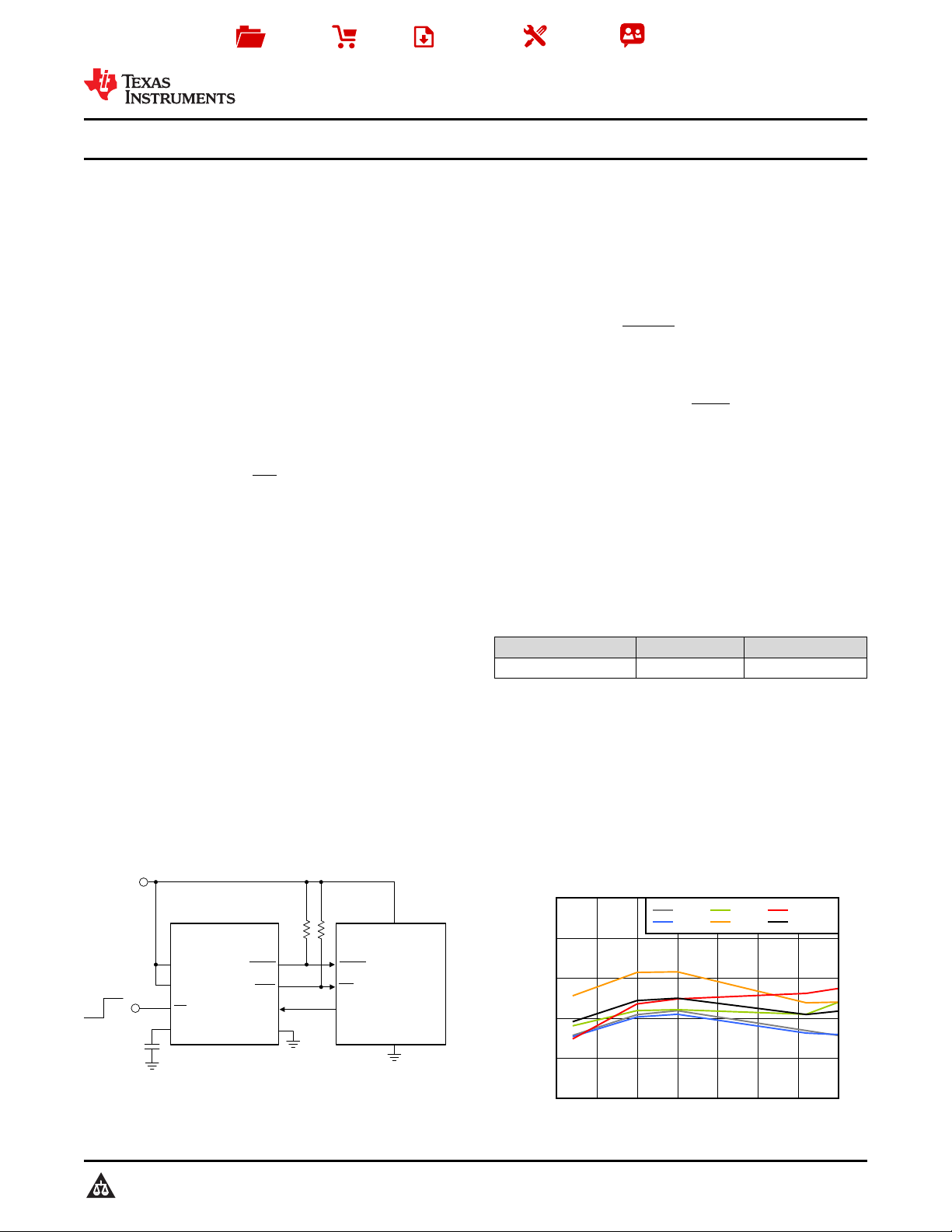
The TPS3852-Q1 is a precision voltage supervisor
with an integrated window watchdog timer. The
TPS3852-Q1 includes a precision undervoltage
supervisor with an undervoltage threshold (V
achieves 0.8% accuracy over the specified
temperature range of –40°C to +125°C. In addition,
the TPS3852-Q1 includes accurate hysteresis making
the device ideal for use with tight tolerance systems.
The supervisor RESET delay features a 15%
accuracy, high-precision delay timer.
The TPS3852-Q1 includes a programmable window
watchdog timer for a wide variety of applications. The
dedicated watchdog output (WDO) enables increased
resolution to help determine the nature of fault
conditions. The watchdog timeouts can be
programmed either by an external capacitor or by
factory-programmed default delay settings. The
watchdog can be disabled to avoid undesired
watchdog timeouts during the development process.
The TPS3852-Q1 is available in a small 3.00-mm ×
3.00-mm, 8-pin VSON package. The TPS3852-Q1
features wettable flanks that allow for easy optical
inspection.
Device Information
PART NUMBER PACKAGE BODY SIZE (NOM)
TPS3852-Q1 VSON (8) 3.00 mm × 3.00 mm
(1) For all available packages, see the orderable addendum at
the end of the data sheet.
(1)
ITN
) that
Typical Application Circuit Undervoltage Threshold (V
1
An IMPORTANT NOTICE at the end of this data sheet addresses availability, warranty, changes, use in safety-critical applications,
intellectual property matters and other important disclaimers. PRODUCTION DATA.
Temperature
) Accuracy vs
ITN
TPS3852-Q1
SBVS285 –FEBRUARY 2017
www.ti.com
Table of Contents
1 Features.................................................................. 1
2 Applications ........................................................... 1
3 Description ............................................................. 1
4 Revision History..................................................... 2
5 Pin Configuration and Functions......................... 3
6 Specifications......................................................... 4
6.1 Absolute Maximum Ratings ...................................... 4
6.2 ESD Ratings.............................................................. 4
6.3 Recommended Operating Conditions....................... 4
6.4 Thermal Information.................................................. 5
6.5 Electrical Characteristics........................................... 5
6.6 Timing Requirements................................................ 6
6.7 Typical Characteristics.............................................. 8
7 Detailed Description............................................ 11
7.1 Overview ................................................................. 11
7.2 Functional Block Diagram ....................................... 11
7.3 Feature Description................................................. 12
4 Revision History
DATE REVISION NOTES
February 2017 * Initial release.
7.4 Device Functional Modes........................................ 15
8 Application and Implementation ........................ 16
8.1 Application Information............................................ 16
8.2 Typical Application ................................................. 19
9 Power Supply Recommendations...................... 22
10 Layout................................................................... 22
10.1 Layout Guidelines ................................................. 22
10.2 Layout Example .................................................... 22
11 Device and Documentation Support ................. 23
11.1 Device Support .................................................... 23
11.2 Receiving Notification of Documentation Updates 23
11.3 Community Resources.......................................... 23
11.4 Trademarks ........................................................... 23
11.5 Electrostatic Discharge Caution............................ 23
11.6 Glossary ................................................................ 23
12 Mechanical, Packaging, and Orderable
Information........................................................... 24
2
Submit Documentation Feedback Copyright © 2017, Texas Instruments Incorporated
Product Folder Links: TPS3852-Q1
1VDD 8 RESET
2CWD 7 WDO
3MR 6 WDI
4GND 5 SET1
Not to scale
Pad
www.ti.com
SBVS285 –FEBRUARY 2017
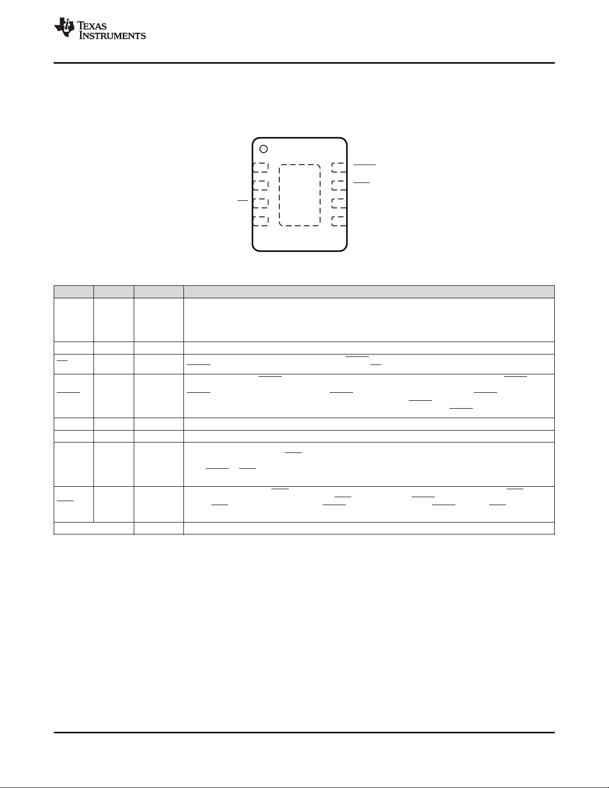
5 Pin Configuration and Functions
DRB Package
8-Pin VSON
Top View
Pin Functions
NAME NO. I/O DESCRIPTION
Programmable watchdog timeout input. Watchdog timeout is set by connecting a capacitor between this pin and
CWD 2 —
GND 4 — Ground pin
MR 3 I
RESET 8 O
SET1 5 I Logic input. Grounding the SET1 pin disables the watchdog timer.
VDD 1 I Supply voltage pin. For noisy systems, connecting a 0.1-μF bypass capacitor is recommended.
WDI 6 I
WDO 7 O
Thermal pad — Connect the thermal pad to a large-area ground plane. The thermal pad is internally connected to GND.
ground. Furthermore, this pin can also be connected by a 10-kΩ resistor to VDD, or leaving unconnected (NC) further
enables the selection of the preset watchdog timeouts; see the Timing Requirements table.
When using a capacitor, the TPS3852-Q1 determines the window watchdog upper boundary with Equation 1.
See Table 4 and the CWD Functionality section for additional information.
Manual reset pin. A logical low on this pin issues a RESET. This pin is internally pulled up to VDD.
RESET remains low for a fixed reset delay (t
) time after MR is deasserted (high).
RST
Reset output. Connect RESET using a 1-kΩ to 100-kΩ resistor to the desired pullup voltage rail (VPU). RESET goes
low when VDDgoes below the undervoltage threshold (V
RESET timeout counter starts. At completion, RESET goes high. During startup, the state of RESET is undefined
below the specified power-on-reset (POR) voltage (V
monitored voltage is within the correct operating range (above V
Watchdog input. A falling transition (edge) must occur at this pin between the lower (t
window boundaries in order for WDO to not assert.
). When VDDis within the normal operating range, the
ITN
). Above POR, RESET goes low and remains low until the
POR
ITN
+ V
) and the RESET timeout is complete.
HYST
) and upper (t
WDL(max)
When the watchdog is not in use, the SET1 pin can be used to disable the watchdog. The input at WDI is ignored
when RESET or WDO are low (asserted) and also when the watchdog is disabled. If the watchdog is disabled, then
WDI cannot be left unconnected and must be driven to either VDD or GND.
Watchdog output. Connect WDO with a 1-kΩ to 100-kΩ resistor to the desired pullup voltage rail (VPU). WDO goes
low (asserts) when a watchdog timeout occurs. WDO only asserts when RESET is high. When a watchdog timeout
occurs, WDO goes low (asserts) for the set RESET timeout delay (t
impedance state.
). When RESET goes low, WDO is in a high-
RST
TPS3852-Q1
)
WDU(min)
Product Folder Links: TPS3852-Q1
Submit Documentation FeedbackCopyright © 2017, Texas Instruments Incorporated
3
TPS3852-Q1
SBVS285 –FEBRUARY 2017
www.ti.com
6 Specifications
6.1 Absolute Maximum Ratings
over operating free-air temperature range (unless otherwise noted)
Supply voltage range VDD –0.3 7 V
Output voltage range RESET, WDO –0.3 7 V
Voltage ranges
Output pin current ±20 mA
Input current (all pins) ±20 mA
Continuous total power dissipation See Thermal Information
Temperature
(1) Stresses beyond those listed under Absolute Maximum Ratings may cause permanent damage to the device. These are stress ratings
only, which do not imply functional operation of the device at these or any other conditions beyond those indicated under Recommended
Operating Conditions. Exposure to absolute-maximum-rated conditions for extended periods may affect device reliability.
(2) The absolute maximum rating is VDD+ 0.3 V or 7.0 V, whichever is smaller.
(3) Assume that TJ= TAas a result of the low dissipated power in this device.
SET1, WDI, MR –0.3 7
CWD, CRST –0.3 VDD+ 0.3
Operating junction, T
Storage, T
stg
(3)
J
(3)
A
(1)
MIN MAX UNIT
(2)
V
–40 150
–40 150
°COperating free-air, T
–65 150
6.2 ESD Ratings
VALUE UNIT
V
(ESD)
Electrostatic discharge
Human-body model (HBM), per AEC Q100-002
Charged-device model (CDM), per AEC Q100-011 ±750
(1)
±2000
(1) AEC Q100-002 indicates that HBM stressing shall be in accordance with the ANSI/ESDA/JEDEC JS-001 specification.
6.3 Recommended Operating Conditions
over operating free-air temperature range (unless otherwise noted)
MIN NOM MAX UNIT
V
DD
V
SET1
V
MR
C
CWD
CWD Pullup resistor to VDD 9 10 11 kΩ
R
PU
I
RESET
I
WDO
T
J
(1) Using a C
Supply pin voltage 1.6 6.5 V
SET1 pin voltage 0 6.5 V
MR pin voltage 0 6.5 V
Watchdog timing capacitor 0.1
(1)
1000
(1)
Pullup resistor, RESET and WDO 1 10 100 kΩ
RESET pin current 10 mA
Watchdog output current 10 mA
Junction temperature –40 125 °C
capacitor of 0.1 nF or 1000 nF gives a t
CWD
of 62.74 ms or 77.45 seconds, respectively.
WDU(typ)
V
nF
4
Submit Documentation Feedback Copyright © 2017, Texas Instruments Incorporated
Product Folder Links: TPS3852-Q1
TPS3852-Q1
www.ti.com
SBVS285 –FEBRUARY 2017
6.4 Thermal Information
TPS3852-Q1
THERMAL METRIC
(1)
UNITDRB (VSON)
8 PINS
R
θJA
R
θJC(top)
R
θJB
ψ
JT
ψ
JB
R
θJC(bot)
Junction-to-ambient thermal resistance 47.7 °C/W
Junction-to-case (top) thermal resistance 51.5 °C/W
Junction-to-board thermal resistance 22.2 °C/W
Junction-to-top characterization parameter 1.3 °C/W
Junction-to-board characterization parameter 22.3 °C/W
Junction-to-case (bottom) thermal resistance 4.3 °C/W
(1) For more information about traditional and new thermal metrics, see the Semiconductor and IC Package Thermal Metrics application
report.
6.5 Electrical Characteristics
at V
+ V
ITN
open-drain pullup resistors are 10 kΩ for each output; typical values are at TJ= 25°C
GENERAL CHARACTERISTICS
(1)
V
DD
I
DD
RESET FUNCTION
(2)
V
POR
(3)
V
UVLO
V
ITN
V
HYST
I
MR
WINDOW WATCHDOG FUNCTION
I
CWD
V
CWD
V
OL
I
D
V
IL
V
IH
V
IL(WDI)
V
IH(WDI)
(1) During power on, VDDmust be a minimum of 1.6 V for at least 300 µs before RESET correlates with VDD.
(2) When VDDfalls below V
(3) When VDDfalls below UVLO, RESET is driven low.
≤ VDD≤ 6.5 V over the operating temperature range of –40°C ≤ TA, TJ≤ +125°C (unless otherwise noted); the
HYST
PARAMETER TEST CONDITIONS MIN TYP MAX UNIT
Supply voltage 1.6 6.5 V
Supply current 10 19 µA
Power-on-reset voltage I
RESET
= 15 µA, V
= 0.25 V 0.8 V
OL(MAX)
Undervoltage lockout voltage 1.35 V
Undervoltage threshold accuracy,
entering RESET
VDDfalling V
– 0.8% V
ITN
ITN
+ 0.8%
Hysteresis voltage VDDrising 0.2% 0.5% 0.8%
MR pin internal pullup current VMR= 0 V 500 620 700 nA
CWD pin charge current CWD = 0.5 V 337 375 413 nA
CWD pin threshold voltage 1.192 1.21 1.228 V
RESET, WDO output low
RESET, WDO output leakage current,
open-drain
VDD = 5 V,
I
= I
RESET
VDD = V
V
= V
RESET
WDO
ITN
+ V
WDO
= 3 mA
HYST
= 6.5 V
0.4 V
,
1 µA
Low-level input voltage (MR, SET1) 0.25 V
High-level input voltage (MR, SET1) 0.8 V
Low-level input voltage (WDI) 0.3 × V
High-level input voltage (WDI) 0.8 × V
, RESET and WDO are undefined.
POR
DD
DD
V
V
Product Folder Links: TPS3852-Q1
Submit Documentation FeedbackCopyright © 2017, Texas Instruments Incorporated
5
VDD
RESET
WDI
WDO
t
RST
t
RST
t
RST
V
POR
V
ITN
t < t
WDU
t
WDL
< t < t
WDU
(1)
t < t
WDL
X
V
ITN
+ V
HYST
V
ITN
X
t
RST-DEL
t < t
WDU
TPS3852-Q1
SBVS285 –FEBRUARY 2017
6.6 Timing Requirements
at V
+ V
ITN
open-drain pullup resistors are 10 kΩ for each output; typical values are at TJ= 25°C
GENERAL
t
INIT
RESET FUNCTION
t
RST
t
RST-DELVDD
t
MR-DEL
Watchdog Function
t
WDL
t
WDU
t
WD-
setup
t
WD-DEL
(1) SET1 = 0 means V
≤ VDD≤ 6.5 V over the operating temperature range of –40°C ≤ TA, TJ≤ +125°C (unless otherwise noted); the
HYST
CWD pin evaluation period 381 µs
Minimum MR, SET1 pin pulse duration 1 µs
Startup delay 300 µs
Reset timeout period 170 200 230 ms
to RESET delay
VDD= V
VDD= V
+ V
ITN
– 2.5% 17
ITN
+ 2.5% 35
HYST
MR to RESET delay 200 ns
(1)
(1)
(1)
(1)
1360 1600 1840 ms
Window watchdog lower boundary
Window watchdog upper boundary
CWD = NC, SET1 = 0
CWD = NC, SET1 = 1
CWD = 10 kΩ to VDD,
SET1 = 0
CWD = 10 kΩ to VDD,
SET1 = 1
(1)
(1)
CWD = NC, SET1 = 0
CWD = NC, SET1 = 1
CWD = 10 kΩ to VDD,
SET1 = 0
CWD = 10 kΩ to VDD,
SET1 = 1
(1)
(1)
Setup time required for device to respond to changes on WDI after
being enabled
Minimum WDI pulse duration 50 ns
WDI to WDO delay 50 ns
< VIL, SET1 = 1 means V
SET1
SET1
> VIH.
www.ti.com
MIN TYP MAX UNIT
µs
Watchdog disabled
680 800 920 ms
Watchdog disabled
1.48 1.85 2.22 ms
Watchdog disabled
Watchdog disabled
9.35 11.0 12.65 ms
150 µs
(1) See Figure 2 for WDI timing requirements.
6
Submit Documentation Feedback Copyright © 2017, Texas Instruments Incorporated
Figure 1. Timing Diagram
Product Folder Links: TPS3852-Q1
t
WDL(min)
Window
Timing
WDI
t
WDL(typ)
t
WDL(max)
t
WDU(min)
t
WDU(typ)
t
WDU(max)
WDO
= Tolerance Window
Early Fault
WDO
Late Fault
WDI
Valid
Window
Correct Operation
WDI
WDO
www.ti.com
TPS3852-Q1
SBVS285 –FEBRUARY 2017
Figure 2. TPS3852-Q1 Window Watchdog Timing
Submit Documentation FeedbackCopyright © 2017, Texas Instruments Incorporated
Product Folder Links: TPS3852-Q1
7
Temperature (qC)
Accuracy (%)
-50 -25 0 25 50 75 100 125
-0.5
-0.3
-0.1
0.1
0.3
0.5
Unit 1
Unit 2
Unit 3
Unit 4
Unit 5
Average
V
ITN
+ V
HYST
Accuracy (%)
Frequency (%)
0
5
10
15
20
25
30
35
40
45
-0.8 -0.6 -0.4 -0.2 0 0.2 0.4 0.6 0.8
Temperature (qC)
CWD Charging Current (nA)
-50 -25 0 25 50 75 100 125
364
368
372
376
380
1.6 V
6.5 V
Temperature (qC)
Accuracy (%)
-50 -25 0 25 50 75 100 125
-0.5
-0.3
-0.1
0.1
0.3
0.5
Unit 1
Unit 2
Unit 3
Unit 4
Unit 5
Average
VDD (V)
Supply Current (PA)
0 1 2 3 4 5 6 7
0
4
8
12
16
-40qC
0qC
25qC
105qC
125qC
Temperature (qC)
Manual Reset Threshold (V)
-50 -25 0 25 50 75 100 125
0.3
0.4
0.5
0.6
0.7
V
IL
V
IH
TPS3852-Q1
SBVS285 –FEBRUARY 2017
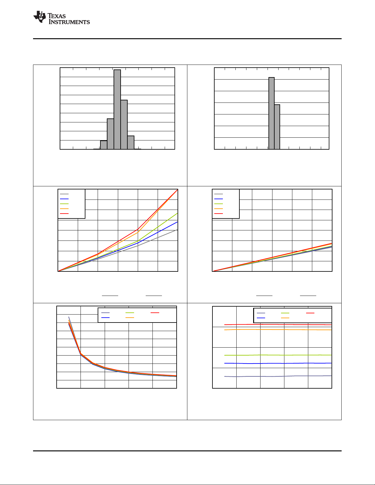
6.7 Typical Characteristics
all curves are taken at 25°C with 1.6 V ≤ VDD ≤ 6.5 V (unless otherwise noted)
www.ti.com
VDD = 1.6 V
Figure 3. Supply Current vs V
DD
Figure 5. CWD Charging Current vs Temperature
Figure 4. MR Threshold vs Temperature
TPS3852G33-Q1
Figure 6. V
ITN
+ V
Accuracy vs Temperature
HYST
8
Figure 7. V
TPS3852G33-Q1
Accuracy vs Temperature
ITN
Submit Documentation Feedback Copyright © 2017, Texas Instruments Incorporated
Includes G and H versions with 3.3-V nominal monitored voltage,
Product Folder Links: TPS3852-Q1
Figure 8. V
total units = 15,536
ITN
+ V
Accuracy Histogram
HYST
Overdrive (%)
Propagation Delay (Ps)
0 2 4 6 8 10
0
5
10
15
20
25
30
35
40
45
50
-40qC
0qC
25qC
105qC
125qC
Overdrive (%)
Propagation Delay (ms)
0 2 4 6 8 10
190
195
200
205
210
-40qC
0qC
25qC
105qC
125qC
I
RESET
(mA)
V
OL
(V)
0 1 2 3 4 5 6
0
0.2
0.4
0.6
0.8
1
1.2
1.4
1.6
-40qC
0qC
25qC
105qC
125qC
I
RESET
(mA)
V
OL
(V)
0 1 2 3 4 5 6
0
0.2
0.4
0.6
0.8
1
1.2
1.4
1.6
-40qC
0qC
25qC
105qC
125qC
V
ITN
Accuracy (%)
Frequency (%)
0
5
10
15
20
25
30
35
40
45
-0.8 -0.6 -0.4 -0.2 0 0.2 0.4 0.6 0.8
Hysteresis (%)
Frequency (%)
0
10
20
30
40
50
60
70
0.2 0.35 0.5 0.65 0.8
www.ti.com
Typical Characteristics (continued)
all curves are taken at 25°C with 1.6 V ≤ VDD ≤ 6.5 V (unless otherwise noted)
TPS3852-Q1
SBVS285 –FEBRUARY 2017
Includes G and H versions with 3.3-V nominal monitored voltage,
total units = 15,536
Figure 9. V
Accuracy Histogram
ITN
VDD = 1.6 V
Figure 11. Low-Level RESET Voltage vs RESET Current
Includes G and H versions with 3.3-V nominal monitored voltage,
total units = 15,536
Figure 10. Hysteresis Histogram
VDD = 6.5 V
Figure 12. Low-Level RESET Voltage vs RESET Current
TPS3852G33-Q1 entering undervoltage
Figure 13. Propagation Delay vs Overdrive
Figure 14. Propagation Delay (t
Product Folder Links: TPS3852-Q1
TPS3852G33-Q1 exiting undervoltage
) vs Overdrive
RST
Submit Documentation FeedbackCopyright © 2017, Texas Instruments Incorporated
9

Temperature (qC)
Glitch Immunity (Ps)
-50 -25 0 25 50 75 100 125
5
10
15
20
25
Overdrive = 3%
Overdrive = 5%
Overdrive = 7%
Overdrive = 9%
Overdrive = 10%
TPS3852-Q1
SBVS285 –FEBRUARY 2017
Typical Characteristics (continued)
all curves are taken at 25°C with 1.6 V ≤ VDD ≤ 6.5 V (unless otherwise noted)
V
= 3.168 V
ITN
Figure 15. High-to-Low Glitch Immunity vs Temperature
www.ti.com
10
Submit Documentation Feedback Copyright © 2017, Texas Instruments Incorporated
Product Folder Links: TPS3852-Q1

VDD
Precision
Clock
State
Machine
Cap
Control
CWD
GND
VDD
WDI
MR SET1
WDO
RESET
Reference
R
1
R
2
Copyright © 2016, Texas Instruments Incorporated
TPS3852-Q1
www.ti.com
SBVS285 –FEBRUARY 2017
7 Detailed Description
7.1 Overview
The TPS3852-Q1 is a high-accuracy voltage supervisor with an integrated window watchdog timer. This device
includes a precision undervoltage supervisor with a threshold that achieves 0.8% accuracy over the specified
temperature range of –40°C to +125°C. In addition, the TPS3852-Q1 includes accurate hysteresis on the
threshold, making the device ideal for use with tight tolerance systems where voltage supervisors must ensure a
RESET before the minimum supply tolerance of the microprocessor or system-on-a-chip (SoC) is reached.
7.2 Functional Block Diagram
NOTE: R1+ R2= 4.5 MΩ.
Product Folder Links: TPS3852-Q1
Submit Documentation FeedbackCopyright © 2017, Texas Instruments Incorporated
11

Undervoltage Limit
VDD
V
ITN
V
ITN
+ V
HYST
RESET
t
RST
+ t
RST-DEL
t
RST-DEL
TPS3852-Q1
SBVS285 –FEBRUARY 2017
www.ti.com
7.3 Feature Description
7.3.1 RESET
Connect RESET to VPUthrough a 1-kΩ to 100-kΩ pullup resistor. RESET remains high (deasserted) when VDDis
greater than the negative threshold voltage (V
asserted, driving the RESET pin to low impedance. When VDDrises above V
enabled that holds RESET low for a specified reset delay period (t
RESET pin goes to a high-impedance state and uses a pullup resistor to hold RESET high. The pullup resistor
must be connected to the desired voltage rail to allow other devices to be connected at the correct interface
voltage. To ensure proper voltage levels, give some consideration when choosing the pullup resistor values. The
pullup resistor value is determined by output logic low voltage (VOL), leakage current (ID), and the current through
the RESET pin I
RESET
.
7.3.2 Manual Reset (MR)
The manual reset (MR) input allows a processor or other logic circuits to initiate a reset. A logic low on MR
causes RESET to assert. After MR returns to a logic high and VDDis above V
after the reset delay time (t
). If MR is not controlled externally, then MR can either be connected to VDDor left
RST
floating because the MR pin is internally pulled up. When MR is asserted, the watchdog is disabled and all
signals input to WDI are ignored.
7.3.3 Undervoltage Fault Detection
The TPS3852-Q1 features undervoltage detection for common rails between 1.8 V and 5 V. The voltage is
monitored on the input rail of the device. If VDDdrops below V
VDDis above V
ITN
+ V
, RESET deasserts after t
HYST
built-in hysteresis that provides some noise immunity and ensures stable operation. Although not required in
most cases, for noisy applications, good analog design practice is to place a 1-nF to 100-nF bypass capacitor
close to the VDD pin to reduce sensitivity to transient voltages on the monitored signal.
). If VDDfalls below the negative threshold (V
ITN
). When the reset delay has elapsed, the
RST
ITN
, then RESET is asserted (driven low). When
ITN
, as shown in Figure 16. The internal comparator has
RST
ITN
+ V
+ V
HYST
), then RESET is
ITN
, a delay circuit is
HYST
, RESET is deasserted
Figure 16. Undervoltage Detection
12
Submit Documentation Feedback Copyright © 2017, Texas Instruments Incorporated
Product Folder Links: TPS3852-Q1

SET1
VDD
RESET
Watchdog
Enabled/Disabled
Disabled
Enabled
Enabled
150 µs
TPS3852-Q1
www.ti.com
SBVS285 –FEBRUARY 2017
Feature Description (continued)
7.3.4 Watchdog Mode
This section provides information for the watchdog mode of operation.
7.3.4.1 SET1
The SET1 pin can enable and disable the watchdog timer. If SET1 is set to GND, the watchdog timer is disabled
and WDI is ignored. When the watchdog is disabled, WDO is in a high-impedance state. If the watchdog timer is
disabled, drive the WDI pin to either GND or VDD to ensure that there is no increase in IDD. When SET1 is logic
high, the watchdog operates normally. The SET1 pin can be changed dynamically; however, if the watchdog is
going from disabled to enabled there is a setup time t
on WDI, as shown in Figure 17.
WD-setup
where the watchdog does not respond to changes
Figure 17. Enabling and Disabling the Watchdog
7.3.4.2 Window Watchdog Timer
This section provides information for the window watchdog mode of operation. A window watchdog is typically
employed in safety-critical applications where a traditional watchdog timer is inadequate. In a traditional
watchdog there is a maximum time in which a pulse must be issued to prevent the reset from occurring. In a
window watchdog, the pulse must be issued between a maximum lower window time (t
upper window time (t
WDU(min)
) set by the CWD pin.
WDL(max)
) and the minimum
7.3.4.3 Watchdog Input (WDI)
WDI is the watchdog timer input that controls the WDO output. The WDI input is triggered by the falling edge of
the input signal. For the first pulse, the watchdog acts as a traditional watchdog timer; thus, the first pulse must
be issued before t
WDU(min)
the WDI pulse within the window of t
. After the first pulse, to ensure proper functionality of the watchdog timer, always issue
WDL(max)
and t
WDU(min)
. If the pulse is issued in this region, then WDO remains
unasserted. Otherwise the device asserts WDO, putting the WDO pin into a low-impedance state.
The watchdog input (WDI) is a digital pin. In order to ensure there is no increase in IDD, drive the WDI pin to
either VDD or GND at all times. Putting the pin to an intermediate voltage can cause an increase in supply
current (IDD) because of the architecture of the digital logic gates. When RESET is asserted, the watchdog is
disabled and all signals input to WDI are ignored. When RESET is no longer asserted, the device resumes
normal operation and no longer ignores the signal on WDI. If the watchdog is disabled, drive the WDI pin to
either VDD or GND.
Product Folder Links: TPS3852-Q1
Submit Documentation FeedbackCopyright © 2017, Texas Instruments Incorporated
13

TPS3852-Q1
SBVS285 –FEBRUARY 2017
www.ti.com
Feature Description (continued)
7.3.4.4 CWD
The CWD pin provides the functionality of both high-precision, factory-programmed window watchdog timing
options and user-programmable window watchdog timing. The CWD pin can be either pulled up to VDDthrough a
resistor, have an external capacitor to ground, or be left floating. Every time that the device issues a reset event
and the supply voltage is above V
the pin. There is an internal state machine that the device goes through to determine which option is connected
to the CWD pin. The state machine can take up to 381 μs to determine if the CWD pin is left floating, pulled-up
through a resistor, or connected to a capacitor.
If the CWD pin is being pulled up to VDDusing a pullup resistor, then use a 10-kΩ resistor.
7.3.4.5 Watchdog Output (WDO)
The TPS3852-Q1 features a window watchdog with an independent watchdog output (WDO). The independent
watchdog output gives the flexibility to flag when there is a fault in the watchdog timing without performing an
entire system reset. For legacy applications, WDO can be tied to RESET. When the RESET output is not
asserted, the WDO signal maintains normal operation. However, when the RESET signal is asserted, the WDO
pin goes to a high-impedance state. This is due to using the standard RESET timing options when a fault occurs
on WDO. When RESET is unasserted, the window watchdog timer resumes normal operation.
, the device tries to determine which of these three options is connected to
ITN
14
Submit Documentation Feedback Copyright © 2017, Texas Instruments Incorporated
Product Folder Links: TPS3852-Q1

www.ti.com
7.4 Device Functional Modes
Table 1 summarises the functional modes of the TPS3852-Q1.
Table 1. Device Functional Modes
V
DD
VDD< V
POR
V
≤ VDD< V
V
DD(min)
POR
≤ VDD≤ V
VDD> V
ITN
ITN
DD(min)
+ V
(2)
HYST
(1)
(1) Only valid before VDDgoes above V
(2) Only valid after VDDgoes above V
(3) Where t
is the time between the falling edges on WDI.
PULSE
WDI WDO RESET
— — Undefined
Ignored High Low
Ignored High Low
t
WDL(max)
t
PULSE
t
PULSE
ITN
ITN
t
WDU(min)
+ V
+ V
> t
< t
HYST
HYST
< t
PULSE
(3)
WDU(min)
WDL(max)
.
.
<
(3)
(3)
TPS3852-Q1
SBVS285 –FEBRUARY 2017
High High
Low High
Low High
7.4.1 VDDis Below V
POR(VDD
When VDDis less than V
< V
, RESET is undefined and can be either high or low. The state of RESET largely
POR
POR
)
depends on the load that the RESET pin is experiencing.
7.4.2 Above Power-On-Reset, But Less Than V
When the voltage on VDDis less than V
DD(min)
and greater than or equal to V
DD(min)(VPOR
≤ VDD< V
DD(min)
POR
)
, the RESET signal is asserted
(logic low). When RESET is asserted, the watchdog output WDO is in a high-impedance state regardless of the
WDI signal that is input to the device.
7.4.3 Normal Operation (VDD≥ V
When VDDis greater than or equal to V
DD(min)
DD(min)
)
, the RESET signal is determined by VDD. When RESET is asserted,
WDO goes to a high-impedance state. WDO is then pulled high through the pullup resistor.
Product Folder Links: TPS3852-Q1
Submit Documentation FeedbackCopyright © 2017, Texas Instruments Incorporated
15

V
DD
C
CWD
Cap
Control
375 nA
CWD
V
DD
CWD
10 k
CWD
User Programmable
Capacitor to GND
10 NŸ5HVLVWRU
to VDD
CWD
Unconnected
TPS3852-Q1 TPS3852-Q1
TPS3852-Q1
V
DD
V
DD
Cap
Control
375 nA
V
DD
Cap
Control
375 nA
V
DD
Copyright © 2016, Texas Instruments Incorporated
TPS3852-Q1
SBVS285 –FEBRUARY 2017
www.ti.com
8 Application and Implementation
NOTE
Information in the following applications sections is not part of the TI component
specification, and TI does not warrant its accuracy or completeness. TI’s customers are
responsible for determining suitability of components for their purposes. Customers should
validate and test their design implementation to confirm system functionality.
8.1 Application Information
8.1.1 CWD Functionality
The TPS3852-Q1 features three options for setting the watchdog window: connecting a capacitor to the CWD
pin, connecting a pullup resistor to VDD, and leaving the CWD pin unconnected. Figure 18 shows a schematic
drawing of all three options. If this pin is connected to VDD through a 10-kΩ pullup resistor or left unconnected
(high impedance), then the factory-programmed watchdog timeouts are enabled; see the Timing Requirements
table. Otherwise, the watchdog timeout can be adjusted by placing a capacitor from the CWD pin to ground.
8.1.1.1 Factory-Programmed Timing Options
If using the factory-programmed timing options (listed in Table 2), the CWD pin must either be unconnected or
pulled up to VDD through a 10-kΩ pullup resistor. Using these options enables high-precision watchdog timing.
INPUT WATCHDOG LOWER BOUNDARY (t
CWD SET1 MIN TYP MAX MIN TYP MAX
NC
10 kΩ to VDD
16
Submit Documentation Feedback Copyright © 2017, Texas Instruments Incorporated
Figure 18. CWD Charging Circuit
Table 2. Factory-Programmed Watchdog Timing
) WATCHDOG UPPER BOUNDARY (t
WDL
0 Watchdog disabled Watchdog disabled
1 680 800 920 1360 1600 1840 ms
0 Watchdog disabled Watchdog disabled
1 1.48 1.85 2.22 9.35 11.0 12.65 ms
Product Folder Links: TPS3852-Q1
WDU
)
UNIT

TPS3852-Q1
www.ti.com
SBVS285 –FEBRUARY 2017
8.1.1.2 Adjustable Capacitor Timing
Adjustable capacitor timing is achievable by connecting a capacitor to the CWD pin. If a capacitor is connected to
CWD, then a 375-nA current source charges C
window watchdog upper boundary with the formula given in Equation 1, where C
t
is in seconds.
WDU
t
(s) = 77.4 × C
WDU(typ)
The TPS3852-Q1 is limited to using C
(µF) + 0.055 (s) (1)
CWD
capacitors between 100 pF and 1 µF. Note that Equation 1 is for ideal
CWD
CWD
until V
= 1.21 V. The TPS3852-Q1 determines the
CWD
is in microfarads (µF) and
CWD
capacitors; capacitor tolerances cause the actual device timing to vary. For the most accurate timing, use
ceramic capacitors with COG dielectric material. As shown in Table 3, when using the minimum capacitance of
100 pF, the watchdog upper boundary is 62.74 ms; whereas with a 1-µF capacitance, the watchdog upper
boundary is 77.455 seconds. If a C
upper boundary (t
). Table 4 shows how t
WDU
capacitor is used, Equation 1 can be used to set the window watchdog
CWD
can be used to calculate t
WDU
WDL
.
C
Table 3. t
CWD
Values for Common Ideal Capacitor Values
WDU
WATCHDOG UPPER BOUNDARY (t
(1)
MIN
TYP MAX
WDU
)
(1)
UNIT
100 pF 53.32 62.74 72.15 ms
1 nF 112.5 132.4 152.2 ms
10 nF 704 829 953 ms
100 nF 6625 7795 8964 ms
1 µF 65836 77455 89073 ms
(1) Minimum and maximum values are calculated using ideal capacitors.
Table 4. Programmable CWD Timing
INPUT WATCHDOG LOWER BOUNDARY (t
CWD SET1 MIN TYP MAX MIN TYP MAX
C
CWD
0 Watchdog disabled Watchdog disabled
1 t
WDU(min)
x 0.5 t
x 0.5 t
WDU
(1) Calculated from Equation 1 using ideal capacitors.
) WATCHDOG UPPER BOUNDARY (t
WDL
WDU(max)
x 0.5 0.85 x t
WDU(typ)
t
WDU(typ)
)
WDU
(1)
1.15 x t
WDU(typ)
UNIT
s
Product Folder Links: TPS3852-Q1
Submit Documentation FeedbackCopyright © 2017, Texas Instruments Incorporated
17

Time
Input Voltage
V
ITN
V
DD
t
1
t
2
ûV1
ûV2
V
ITN
+ V
HYST
Copyright © 2016, Texas Instruments Incorporated
TPS3852-Q1
SBVS285 –FEBRUARY 2017
www.ti.com
8.1.2 Overdrive Voltage
Forcing a RESET is dependent on two conditions: the amplitude VDDis beyond the trip point (ΔV1and ΔV2), and
the length of time that the voltage is beyond the trip point (t1and t2). If the voltage is just under the trip point for a
long period of time, RESET asserts and the output is pulled low. However, if VDDis just under the trip point for a
few nanoseconds, RESET does not assert and the output remains high. The length of time required for RESET
to assert can be changed by increasing the amount VDDgoes under the trip point. If VDDis under the trip point by
10%, the amount of time required for the comparator to respond is much faster and causes RESET to assert
much quicker than when barely under the trip point voltage. Equation 2 shows how to calculate the percentage
overdrive.
Overdrive = |( VDD/ V
In Equation 2, V
is used. V
ITN
corresponds to the threshold trip point. If VDDis exceeding the positive threshold, V
ITX
is used when VDDis falling below the negative threshold. In Figure 19, t1and t2correspond to the
amount of time that VDDis over the threshold; the propagation delay versus overdrive for V
– 1) × 100% | (2)
ITX
+ V
ITN
ITN
and V
ITN
+ V
HYST
HYST
is
illustrated in Figure 13 and Figure 14, respectively.
The TPS3852-Q1 is relatively immune to short positive and negative transients on VDD because of the overdrive
voltage.
Figure 19. Overdrive Voltage
18
Submit Documentation Feedback Copyright © 2017, Texas Instruments Incorporated
Product Folder Links: TPS3852-Q1

V
DD
GND
TPS3852-Q1
3.3 V
Microcontroller
SET1
V
CORE
GND
CWD
WDI GPIO
V
DD
GND
TPS3890-Q1
SENSE
CT
100 k
100 k
100 k
2.2 nF
6.8 µF
Copyright © 2016, Texas Instruments Incorporated
MR
RESET
MR
RESET
WDO
NMI
RESET
TPS3852-Q1
www.ti.com
SBVS285 –FEBRUARY 2017
8.2 Typical Application
A typical application for the TPS3852-Q1 is shown in Figure 20. The TPS3852G33-Q1 is used to monitor the
3.3-V, V
8.2.1 Design Requirements
rail powering the microcontroller.
CORE
Figure 20. Monitoring Supply Voltage and Watchdog Supervision of a Microcontroller
PARAMETER DESIGN REQUIREMENT DESIGN RESULT
Watchdog disable for
initialization period
Watchdog must remain disabled for 7 seconds until
logic enables the watchdog timer
7.21 seconds (typ)
Output logic voltage 3.3-V CMOS 3.3-V CMOS
Monitored rail 3.3 V with a 5% threshold
Watchdog window 250 ms, maximum t
Maximum device current
consumption
50 µA
Worst-case V
(–4.7% threshold)
WDL(max)
= 135 ms, t
52 µA (worst-case) when RESET or WDO is
asserted
= 3.142 V
ITN
WDU(min)
(1)
= 181 ms
(1) Only includes the TPS3852G33-Q1 current consumption.
8.2.2 Detailed Design Procedure
8.2.2.1 Monitoring the 3.3-V Rail
This application calls for very tight monitoring of the rail with only 5% of variation allowed on the rail. To ensure
this requirement is met, the TPS3852G33-Q1 was chosen for its –4% threshold. To calculate the worst-case for
V
, the accuracy must also be taken into account. The worst-case for V
ITN
V
ITN(Worst-Case)
= V
× 0.992 = 3.3 × 0.96 × 0.992 = 3.142 V (3)
ITN(typ)
can be calculated by Equation 3:
ITN
Product Folder Links: TPS3852-Q1
Submit Documentation FeedbackCopyright © 2017, Texas Instruments Incorporated
19

3
WDL(MAX) WDU(MAX)
t 0.5 t 0.5 1.15 77.4 2.2 10 0.055 129ms
ª º
u u u u u
¬ ¼
3
WDU(MIN) WDU(TYP)
t 0.85 t 0.85 77.4 2.2 10 0.055 191 ms
u u u u
WDU
CWD
t 0.055
0.25 0.055
C F 0.0025 F
77.4 77.4
P P
RESET
V
PU
RESET
CONTROL
Copyright © 2016, Texas Instruments Incorporated
TPS3852-Q1
SBVS285 –FEBRUARY 2017
www.ti.com
8.2.2.2 Calculating RESET and the WDO Pullup Resistor
The TPS3852-Q1 uses an open-drain configuration for the RESET circuit, as shown in Figure 21. When the FET
is off, the resistor pulls the drain of the transistor to VDD and when the FET is turned on, the FET attempts to
pull the drain to ground, thus creating an effective resistor divider. The resistors in this divider must be chosen to
ensure that VOLis below the maximum value. To choose the proper pullup resistor, there are three key
specifications to keep in mind: the pullup voltage (VPU), the recommended maximum RESET pin current (I
RESET
and VOL. The maximum VOLis 0.4 V, meaning that the effective resistor divider created must be able to bring the
voltage on the reset pin below 0.4 V with I
resistor must be chosen to keep I
below 50 μA because this value is the maximum consumption current
RESET
kept below 10 mA. For this example, with a VPUof 3.3 V, a
RESET
allowed. To ensure this specification is met, a pullup resistor value of 100 kΩ was selected, which sinks a
maximum of 33 μA when RESET or WDO is asserted. As illustrated in Figure 11, when the RESET current is at
33 μA the low-level output voltage is approximately zero.
Figure 21. RESET Open-Drain Configuration
),
8.2.2.3 Setting the Window Watchdog
As illustrated in Figure 18, there are three options for setting the window watchdog. The design specifications in
this application require the programmable timing option (external capacitor connected to CWD). When a
capacitor is connected to the CWD pin, the window is governed by Equation 4. Equation 4 is only valid for ideal
capacitors, any temperature or voltage derating must be accounted for separately.
(4)
The nearest standard capacitor value to 2.5 nF is 2.2 nF. Selecting 2.2 nF for the C
capacitor gives the
CWD
following minimum and maximum timing parameters:
(5)
(6)
Capacitor tolerance also influence t
WDU(MIN)
and t
WDL(MAX)
. Select a ceramic COG dielectric capacitor for high
accuracy. For 2.2 nF, COG capacitors are readily available with a 5% tolerance, which results in a 5% decrease
in t
WDU(MIN)
and a 5% increase in t
WDL(MAX)
, giving 181 ms and 135 ms, respectively. A falling edge must be
issued within this window.
8.2.2.4 Watchdog Disabled During Initialization Period
The watchdog is often needed to be disabled during startup to allow for an initialization period. When the
initialization period is over, the watchdog timer is turned back on to allow the microcontroller to be monitored by
the TPS3852-Q1. To achieve this setup, SET1 must start at GND. In this design, SET1 is controlled by a
TPS3890-Q1 supervisor. In this application, the TPS3890-Q1 was chosen to monitor VDDas well, meaning that
RESET on the TPS3890-Q1 stays low until VDDrises above V
. When VDDcomes up, the delay time can be
ITN
adjusted through the CT capacitor on the TPS3890-Q1. With this approach, the RESET delay can be adjusted
from a minimum of 25 µs to a maximum of 30 seconds. For this design, a minimum delay of 7 seconds is needed
until the watchdog timer is enabled. The CT capacitor calculation (see the TPS3890-Q1 data sheet) yields an
ideal capacitance of 6.59 µF, giving a closest standard ceramic capacitor value of 6.8 µF. When connecting a
6.8-µF capacitor from CT to GND, the typical delay time is 7.21 seconds. Figure 22 illustrates the typical startup
waveform for this circuit when the watchdog input is off. Figure 22 illustrates that when the watchdog is disabled,
the WDO output remains high. See the TPS3890-Q1 data sheet for detailed information on the TPS3890-Q1.
20
Submit Documentation Feedback Copyright © 2017, Texas Instruments Incorporated
Product Folder Links: TPS3852-Q1

VDD
1V/div
(yellow)
RESET
1V/div
(green)
2µs/div
5.2 µs
VDD
1V/div
RESET
2V/div
204 ms
50ms/div
WDI
2V/div
VDD
2V/div
WDO
2V/div
RESET
2V/div
128 ms
50ms/div
VDD
2V/div
SET1
2V/div
WDO
2V/div
RESET
2V/div
7.94 s
1s/div
TPS3852-Q1
www.ti.com
SBVS285 –FEBRUARY 2017
8.2.3 Glitch Immunity
Figure 25 shows the high-to-low glitch immunity for the TPS3852G33-Q1 with a 7% overdrive with VDDstarting at
3.3 V. This curve shows that VDDcan go below the threshold for 5.2 µs without RESET asserting.
8.2.4 Application Curves
Unless otherwise stated, application curves were taken at TA= 25°C.
Figure 22. Startup Without a WDI Signal
Figure 24. Typical RESET Delay
Figure 23. Typical WDI Signal
Figure 25. High-to-Low Glitch Immunity
Product Folder Links: TPS3852-Q1
Submit Documentation FeedbackCopyright © 2017, Texas Instruments Incorporated
21

1
2
3
4
7
6
5
VDD
CWD
MR
GND
WDO
WDI
SET1
GND Plane
8
RESET
Vin
R
PU2
C
VDD
C
CWD
Vin
R
PU1
Vin
Denotes a via
TPS3852-Q1
SBVS285 –FEBRUARY 2017
www.ti.com
9 Power Supply Recommendations
This device is designed to operate from an input supply with a voltage range between 1.6 V and 6.5 V. An input
supply capacitor is not required for this device; however, if the input supply is noisy, then good analog practice is
to place a 0.1-µF capacitor between the VDD pin and the GND pin.
10 Layout
10.1 Layout Guidelines
• Make sure that the connection to the VDD pin is low impedance. Good analog design practice is to place a
0.1-µF ceramic capacitor as near as possible to the VDD pin.
• If a C
If the CWD pin is left unconnected, make sure to minimize the amount of parasitic capacitance on the pin.
• Place the pullup resistors on RESET and WDO as close to the pin as possible.
10.2 Layout Example
capacitor or pull-up resistor is used, place these components as close as possible to the CWD pin.
CWD
Figure 26. Typical Layout for the TPS3852-Q1
22
Submit Documentation Feedback Copyright © 2017, Texas Instruments Incorporated
Product Folder Links: TPS3852-Q1

TPS3852-Q1
www.ti.com
SBVS285 –FEBRUARY 2017
11 Device and Documentation Support
11.1 Device Support
11.1.1 Development Support
11.1.1.1 Evaluation Module
The TPS3851EVM-780 Evaluation Module can be used to evaluate this part. If this evaluation module is being
used, then the device on the EVM must be changed to the TPS3852-Q1.
11.1.2 Device Nomenclature
Table 5. Device Nomenclature
DESCRIPTION NOMENCLATURE VALUE
(high-accuracy supervisor with window watchdog)
(nominal threshold as a percent of the nominal
(nominal monitored voltage option)
(1) For example, the TPS3852G33QDRBQ1 corresponds to a 3.3-V nominal monitored voltage with a –4% nominal threshold.
TPS3852
X
monitored voltage)
(1)
yy(y)
— —
G V
H V
18 1.8 V
33 3.3 V
ITN
ITN
= –4%
= –7%
11.2 Receiving Notification of Documentation Updates
To receive notification of documentation updates, navigate to the device product folder on ti.com. In the upper
right corner, click on Alert me to register and receive a weekly digest of any product information that has
changed. For change details, review the revision history included in any revised document.
11.3 Community Resources
The following links connect to TI community resources. Linked contents are provided "AS IS" by the respective
contributors. They do not constitute TI specifications and do not necessarily reflect TI's views; see TI's Terms of
Use.
TI E2E™ Online Community TI's Engineer-to-Engineer (E2E) Community. Created to foster collaboration
among engineers. At e2e.ti.com, you can ask questions, share knowledge, explore ideas and help
solve problems with fellow engineers.
Design Support TI's Design Support Quickly find helpful E2E forums along with design support tools and
contact information for technical support.
11.4 Trademarks
E2E is a trademark of Texas Instruments.
All other trademarks are the property of their respective owners.
11.5 Electrostatic Discharge Caution
This integrated circuit can be damaged by ESD. Texas Instruments recommends that all integrated circuits be handled with
appropriate precautions. Failure to observe proper handling and installation procedures can cause damage.
ESD damage can range from subtle performance degradation to complete device failure. Precision integrated circuits may be more
susceptible to damage because very small parametric changes could cause the device not to meet its published specifications.
11.6 Glossary
SLYZ022 — TI Glossary.
This glossary lists and explains terms, acronyms, and definitions.
Product Folder Links: TPS3852-Q1
Submit Documentation FeedbackCopyright © 2017, Texas Instruments Incorporated
23

TPS3852-Q1
SBVS285 –FEBRUARY 2017
www.ti.com
12 Mechanical, Packaging, and Orderable Information
The following pages include mechanical, packaging, and orderable information. This information is the most
current data available for the designated devices. This data is subject to change without notice and revision of
this document. For browser-based versions of this data sheet, refer to the left-hand navigation.
24
Submit Documentation Feedback Copyright © 2017, Texas Instruments Incorporated
Product Folder Links: TPS3852-Q1

PACKAGE OPTION ADDENDUM
www.ti.com
10-Dec-2020
PACKAGING INFORMATION
Orderable Device Status
TPS3852G18QDRBRQ1 ACTIVE SON DRB 8 3000 RoHS & Green SN Level-2-260C-1 YEAR -40 to 125 852DB
TPS3852G33QDRBRQ1 ACTIVE SON DRB 8 3000 RoHS & Green SN Level-2-260C-1 YEAR -40 to 125 852GB
TPS3852H18QDRBRQ1 ACTIVE SON DRB 8 3000 RoHS & Green SN Level-2-260C-1 YEAR -40 to 125 852LB
TPS3852H33QDRBRQ1 ACTIVE SON DRB 8 3000 RoHS & Green SN Level-2-260C-1 YEAR -40 to 125 852PB
(1)
The marketing status values are defined as follows:
ACTIVE: Product device recommended for new designs.
LIFEBUY: TI has announced that the device will be discontinued, and a lifetime-buy period is in effect.
NRND: Not recommended for new designs. Device is in production to support existing customers, but TI does not recommend using this part in a new design.
PREVIEW: Device has been announced but is not in production. Samples may or may not be available.
OBSOLETE: TI has discontinued the production of the device.
Package Type Package
(1)
Drawing
Pins Package
Qty
Eco Plan
(2)
Lead finish/
Ball material
(6)
MSL Peak Temp
(3)
Op Temp (°C) Device Marking
(4/5)
(2)
RoHS: TI defines "RoHS" to mean semiconductor products that are compliant with the current EU RoHS requirements for all 10 RoHS substances, including the requirement that RoHS substance
do not exceed 0.1% by weight in homogeneous materials. Where designed to be soldered at high temperatures, "RoHS" products are suitable for use in specified lead-free processes. TI may
reference these types of products as "Pb-Free".
RoHS Exempt: TI defines "RoHS Exempt" to mean products that contain lead but are compliant with EU RoHS pursuant to a specific EU RoHS exemption.
Green: TI defines "Green" to mean the content of Chlorine (Cl) and Bromine (Br) based flame retardants meet JS709B low halogen requirements of <=1000ppm threshold. Antimony trioxide based
flame retardants must also meet the <=1000ppm threshold requirement.
(3)
MSL, Peak Temp. - The Moisture Sensitivity Level rating according to the JEDEC industry standard classifications, and peak solder temperature.
(4)
There may be additional marking, which relates to the logo, the lot trace code information, or the environmental category on the device.
(5)
Multiple Device Markings will be inside parentheses. Only one Device Marking contained in parentheses and separated by a "~" will appear on a device. If a line is indented then it is a continuation
of the previous line and the two combined represent the entire Device Marking for that device.
(6)
Lead finish/Ball material - Orderable Devices may have multiple material finish options. Finish options are separated by a vertical ruled line. Lead finish/Ball material values may wrap to two
lines if the finish value exceeds the maximum column width.
Important Information and Disclaimer:The information provided on this page represents TI's knowledge and belief as of the date that it is provided. TI bases its knowledge and belief on information
provided by third parties, and makes no representation or warranty as to the accuracy of such information. Efforts are underway to better integrate information from third parties. TI has taken and
Samples
Addendum-Page 1

PACKAGE OPTION ADDENDUM
www.ti.com
continues to take reasonable steps to provide representative and accurate information but may not have conducted destructive testing or chemical analysis on incoming materials and chemicals.
TI and TI suppliers consider certain information to be proprietary, and thus CAS numbers and other limited information may not be available for release.
10-Dec-2020
In no event shall TI's liability arising out of such information exceed the total purchase price of the TI part(s) at issue in this document sold by TI to Customer on an annual basis.
OTHER QUALIFIED VERSIONS OF TPS3852-Q1 :
Catalog: TPS3852
•
NOTE: Qualified Version Definitions:
Catalog - TI's standard catalog product
•
Addendum-Page 2

PACKAGE MATERIALS INFORMATION
www.ti.com 5-Jan-2021
TAPE AND REEL INFORMATION
*All dimensions are nominal
Device Package
TPS3852G18QDRBRQ1 SON DRB 8 3000 330.0 12.4 3.3 3.3 1.0 8.0 12.0 Q2
TPS3852G33QDRBRQ1 SON DRB 8 3000 330.0 12.4 3.3 3.3 1.0 8.0 12.0 Q2
TPS3852H18QDRBRQ1 SON DRB 8 3000 330.0 12.4 3.3 3.3 1.0 8.0 12.0 Q2
TPS3852H33QDRBRQ1 SON DRB 8 3000 330.0 12.4 3.3 3.3 1.0 8.0 12.0 Q2
Type
Package
Drawing
Pins SPQ Reel
Diameter
(mm)
Reel
Width
W1 (mm)
A0
(mm)B0(mm)K0(mm)P1(mm)W(mm)
Quadrant
Pin1
Pack Materials-Page 1

PACKAGE MATERIALS INFORMATION
www.ti.com 5-Jan-2021
*All dimensions are nominal
Device Package Type Package Drawing Pins SPQ Length (mm) Width (mm) Height (mm)
TPS3852G18QDRBRQ1 SON DRB 8 3000 367.0 367.0 38.0
TPS3852G33QDRBRQ1 SON DRB 8 3000 367.0 367.0 38.0
TPS3852H18QDRBRQ1 SON DRB 8 3000 367.0 367.0 38.0
TPS3852H33QDRBRQ1 SON DRB 8 3000 367.0 367.0 38.0
Pack Materials-Page 2


PACKAGE OUTLINE
PIN 1 INDEX AREA
1 MAX
0.05
0.00
SCALE 4.000
VSON - 1 mm max heightDRB0008F
PLASTIC SMALL OUTLINE - NO LEAD
A
3.1
2.9
B
3.1
2.9
0.1 MIN
(0.05)
SECTION A-A
SCALE 30.000
SECTION A-A
TYPICAL
C
SEATING PLANE
0.08 C
EXPOSED
THERMAL PAD
4
1.6 0.05
(0.2) TYP
5
A
A
2X
1.95
6X 0.65
(OPTIONAL)
PIN 1 ID
1
0.5
8X
0.3
8
2.4 0.05
0.35
8X
0.25
0.1 C A B
0.05
C
4222121/C 10/2016
NOTES:
1. All linear dimensions are in millimeters. Any dimensions in parenthesis are for reference only. Dimensioning and tolerancing
per ASME Y14.5M.
2. This drawing is subject to change without notice.
3. The package thermal pad must be soldered to the printed circuit board for thermal and mechanical performance.
www.ti.com

8X (0.6)
8X (0.3)
EXAMPLE BOARD LAYOUT
VSON - 1 mm max heightDRB0008F
PLASTIC SMALL OUTLINE - NO LEAD
(1.6)
SYMM
1
8
(2.4)
6X (0.65)
(R0.05) TYP
( 0.2) VIA
TYP
SOLDER MASK
OPENING
4
0.07 MAX
ALL AROUND
METAL
NON SOLDER MASK
DEFINED
(PREFERRED)
(0.55)
(2.8)
LAND PATTERN EXAMPLE
SCALE:20X
METAL UNDER
SOLDER MASK
(0.95)
5
0.07 MIN
ALL AROUND
SOLDER MASK
OPENING
SOLDER MASK
DEFINED
SOLDER MASK DETAILS
4222121/C 10/2016
NOTES: (continued)
4. This package is designed to be soldered to a thermal pad on the board. For more information, see Texas Instruments literature
number SLUA271 (www.ti.com/lit/slua271).
5. Vias are optional depending on application, refer to device data sheet. If any vias are implemented, refer to their locations shown
on this view. It is recommended that vias under paste be filled, plugged or tented.
www.ti.com

EXAMPLE STENCIL DESIGN
VSON - 1 mm max heightDRB0008F
PLASTIC SMALL OUTLINE - NO LEAD
8X (0.6)
8X (0.3)
SYMM
6X (0.65)
(R0.05) TYP
SYMM
1
4
(1.47)
(2.8)
METAL
TYP
8
(0.635)
(1.07)
5
SOLDER PASTE EXAMPLE
BASED ON 0.125 mm THICK STENCIL
82% PRINTED SOLDER COVERAGE BY AREA
EXPOSED PAD
SCALE:25X
4222121/C 10/2016
NOTES: (continued)
6. Laser cutting apertures with trapezoidal walls and rounded corners may offer better paste release. IPC-7525 may have alternate
design recommendations.
www.ti.com

IMPORTANT NOTICE AND DISCLAIMER
TI PROVIDES TECHNICAL AND RELIABILITY DATA (INCLUDING DATASHEETS), DESIGN RESOURCES (INCLUDING REFERENCE
DESIGNS), APPLICATION OR OTHER DESIGN ADVICE, WEB TOOLS, SAFETY INFORMATION, AND OTHER RESOURCES “AS IS”
AND WITH ALL FAULTS, AND DISCLAIMS ALL WARRANTIES, EXPRESS AND IMPLIED, INCLUDING WITHOUT LIMITATION ANY
IMPLIED WARRANTIES OF MERCHANTABILITY, FITNESS FOR A PARTICULAR PURPOSE OR NON-INFRINGEMENT OF THIRD
PARTY INTELLECTUAL PROPERTY RIGHTS.
These resources are intended for skilled developers designing with TI products. You are solely responsible for (1) selecting the appropriate
TI products for your application, (2) designing, validating and testing your application, and (3) ensuring your application meets applicable
standards, and any other safety, security, or other requirements. These resources are subject to change without notice. TI grants you
permission to use these resources only for development of an application that uses the TI products described in the resource. Other
reproduction and display of these resources is prohibited. No license is granted to any other TI intellectual property right or to any third party
intellectual property right. TI disclaims responsibility for, and you will fully indemnify TI and its representatives against, any claims, damages,
costs, losses, and liabilities arising out of your use of these resources.
TI’s products are provided subject to TI’s Terms of Sale (https:www.ti.com/legal/termsofsale.html) or other applicable terms available either
on ti.com or provided in conjunction with such TI products. TI’s provision of these resources does not expand or otherwise alter TI’s
applicable warranties or warranty disclaimers for TI products.IMPORTANT NOTICE
Mailing Address: Texas Instruments, Post Office Box 655303, Dallas, Texas 75265
Copyright © 2021, Texas Instruments Incorporated
 Loading...