

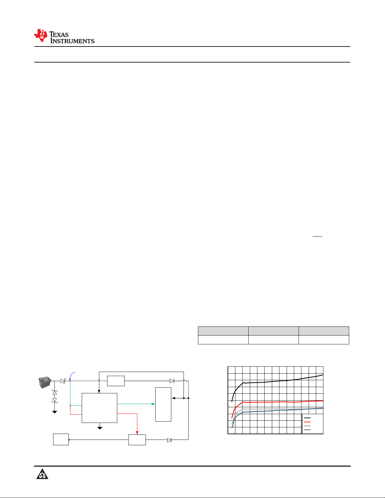
DC/DC
MCU
Low Iq, No external
resistors needed
GND
Boost
Converter
MCU Flag
Enable
Boost
SENSE1
SENSE2
RESET1
RESET2
Backup
Vbatt
VDD
GND
VDD
GPIO
TPS37X
Supply Voltage (V)
Quiescent Current (µA)
0 5 10 15 20 25 30 35 40 45 50 55 60 65
0.5
0.55
0.6
0.65
0.7
0.75
0.8
0.85
0.9
0.95
1
IqNO
125 C
25 C
85 C
-40 C
www.ti.com
ADVANCE INFORMATION
SNVSBD9A – AUGUST 2020 – REVISED JANUARY 2021
SNVSBD9A – AUGUST 2020 – REVISED JANUARY 2021
TPS37x-Q1 (65 V & 2 µA) Over & Undervoltage Detector with Delay Function
TPS37X-Q1
TPS37X-Q1
1 Features
• AEC-Q100 qualified with the following results:
– Device temperature grade 1: –40°C to +125°C
ambient operating temperature
– Device HBM ESD classification level 2
– Device CDM ESD classification level C7B
• VDD: 2.7 V to 65 V (V
POR
= 1.4 V)
• SENSE and RESET pins are 65 V graded
• Low supply current: 1 µA (Typ.)
• Flexible voltage options Table 14-2
– 2.7 V to 36 V (1.5% max accuracy)
– 800 mV option (1% max accuracy)
• Built-in hysteresis (V
HYS
)
– Percentage options: 2% to 13% (1% steps)
– Fixed options: VTH < 8 V = 0.5 V, 1 V, 1.5 V,
2 V, 2.5 V
• Programmable reset time delay
– 10 nF = 12.8 ms, 10 μF = 12.8 s
• Programmable sense time delay
– 10 nF = 1.28 ms, 10 μF = 1.28 s
• Manual reset feature
• Output reset latching feature
• Output topology:
– Channel 1: Open-Drain or Push-Pull topologies
– Channel 2: Open-Drain
2 Applications
• Telematics control unit
• Emergency call system
• Audio amplifier
• Head unit and cluster
• Sensor fusion and cameras
• Body control module
3 Description
The TPS37x-Q1 is a 65 V-input voltage detector with
1 μA IDD, 1% accuracy, and 10 μs detection time in a
6.25 mm2 package. This device can be connected
directly to 12 V / 24 V automotive battery system for
continous monitoring of over (OV) and under (UV)
voltage conditions; with its internal resistor divider, it
offers the smallest total solution size. Wide hysteresis
voltage options are available to ignore cold crank,
start-stop and various car battery voltage transients.
Built-in hysteresis on the SENSE pins prevents false
reset signals when monitoring a supply voltage rail.
The separate VDD and SENSE pins allow for the
redundancy sought by high-reliability automotive
systems and SENSE can monitor higher and lower
voltages than VDD. Optional use of external resistors
are supported by the high impedance input of the
SENSE pins. Both CTSx and CTRx provide delay
adjustability on the rising and falling edges of the
RESET signals. Also, CTSx functions as a debouncer
by ignoring voltage glitches on the monitored voltage
rails; CTRx operates as a manual reset (MR) that can
be used to force a system reset.
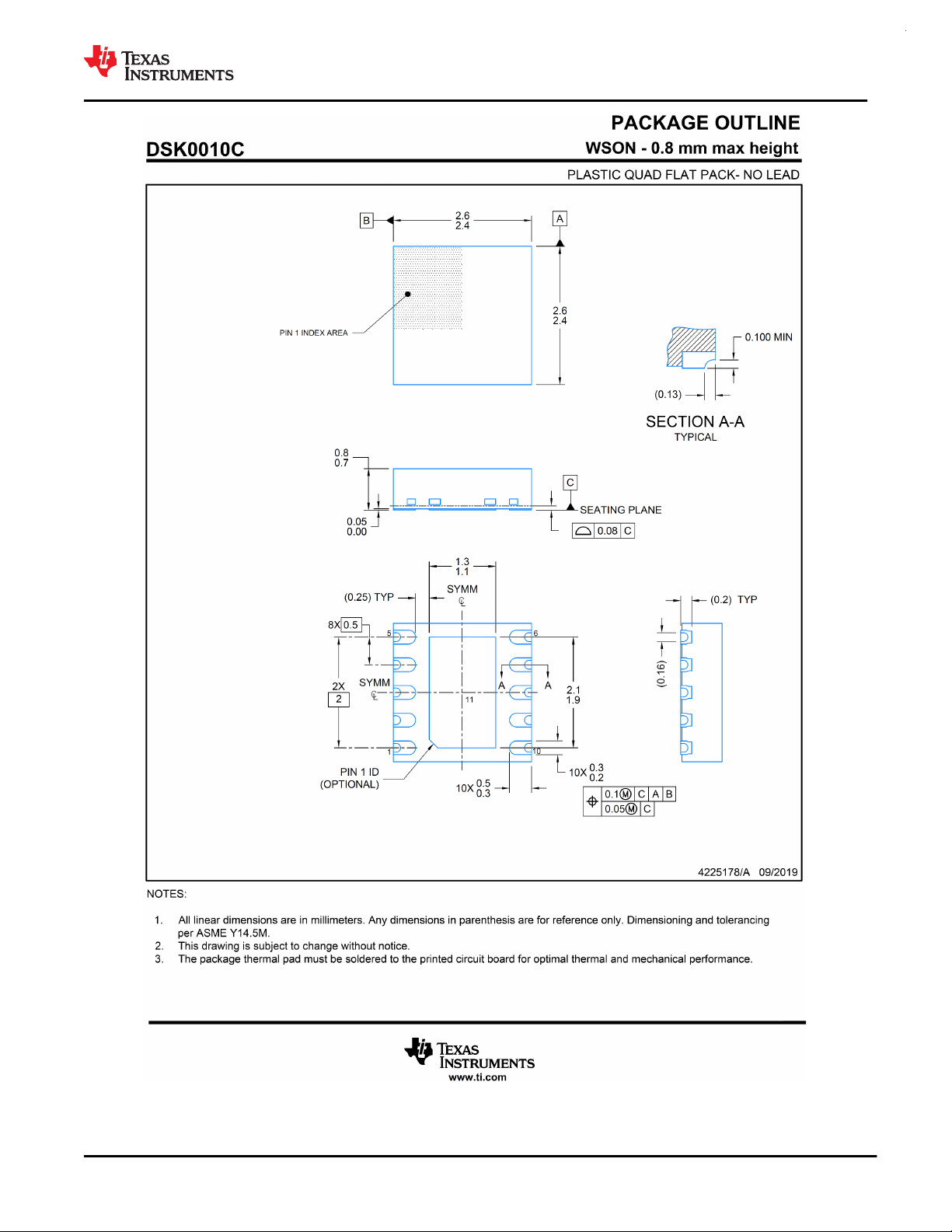
The TPS37x-Q1 is available in a small 2.5-mm×2.5mm×0.1-mm WSON 10-pin wettable flanks package
allowing the facillitation for Automatic Optical
Inspection (AOI) and low resolution X-ray inspection.
The central pad is non-conductive to increase the
creepage between VDD and GND per guidelines in
IEC60664. TPS37x-Q1 operates over –40°C to
+125°C (TA).
Device Information
PART NUMBER PACKAGE
TPS37x-Q1 WSON (10) (DSK) 2.5 mm × 2.5 mm
(1) For package details, see the mechanical drawing addendum
at the end of the data sheet.
(1)
BODY SIZE (NOM)
An IMPORTANT NOTICE at the end of this data sheet addresses availability, warranty, changes, use in safety-critical applications,
Copyright © 2021 Texas Instruments Incorporated
intellectual property matters and other important disclaimers. ADVANCE INFORMATION for preproduction products; subject to change
without notice.
Typical Application Circuit
Typical Supply Current vs VDD
Product Folder Links: TPS37X-Q1
Submit Document Feedback
1

TPS37X-Q1
ADVANCE INFORMATION
SNVSBD9A – AUGUST 2020 – REVISED JANUARY 2021
www.ti.com
Table of Contents
1 Features............................................................................1
2 Applications..................................................................... 1
3 Description.......................................................................1
4 Revision History.............................................................. 2
5 Device Comparison......................................................... 3
6 Pin Configuration and Functions...................................4
7 Specifications.................................................................. 6
7.1 Absolute Maximum Ratings ....................................... 6
7.2 ESD Ratings .............................................................. 6
7.3 Recommended Operating Conditions ........................6
7.4 Thermal Information ...................................................6
7.5 Electrical Characteristics ............................................7
7.6 Timing Requirements .................................................9
8 Typical Characteristics................................................. 10
9 Detailed Description...................................................... 11
9.1 Overview................................................................... 11
9.2 Functional Block Diagram......................................... 11
9.3 Feature Description...................................................12
10 Device Functional Modes........................................... 18
11 Application and Implementation................................ 19
11.1 Adjustable Voltage Thresholds................................19
11.2 Application Information............................................19
11.3 Typical Application.................................................. 20
12 Power Supply Recommendations..............................22
12.1 Power Dissipation and Device Operation............... 22
13 Layout...........................................................................23
13.1 Layout Guidelines................................................... 23
13.2 Layout Example...................................................... 23
13.3 Creepage Distance................................................. 23
14 Device and Documentation Support..........................24
14.1 Device Nomenclature..............................................24
14.2 Support Resources................................................. 26
14.3 Trademarks.............................................................26
14.4 Electrostatic Discharge Caution..............................26
14.5 Glossary..................................................................26
15 Mechanical, Packaging, and Orderable
Information.................................................................... 26
4 Revision History
NOTE: Page numbers for previous revisions may differ from page numbers in the current version.
Changes from Revision * (August 2020) to Revision A (January 2021) Page
• APL Update........................................................................................................................................................ 1
• Added Typical Supply Current vs VDD Curve and modified Description section............................................... 1
• Edited Device Comparison Table........................................................................................................................3
• Edited both Power Cycle figures (SENSE Outside and Within Nominal Voltage)............................................ 12
• Corrected the Hysteresis titles for both Undervoltage figures.......................................................................... 14
• Corrected Channel 1 of TPS37E from Open-Drain Low to Open-Drain High in Output Logic table.................15
• Added reset time delay discharge guideline..................................................................................................... 16
• Added sense time delay discharge guideline................................................................................................... 16
• Added Device Functional Modes tables........................................................................................................... 18
• Added correct Package Outline figure.............................................................................................................. 26
2 Submit Document Feedback
Copyright © 2021 Texas Instruments Incorporated
Product Folder Links: TPS37X-Q1
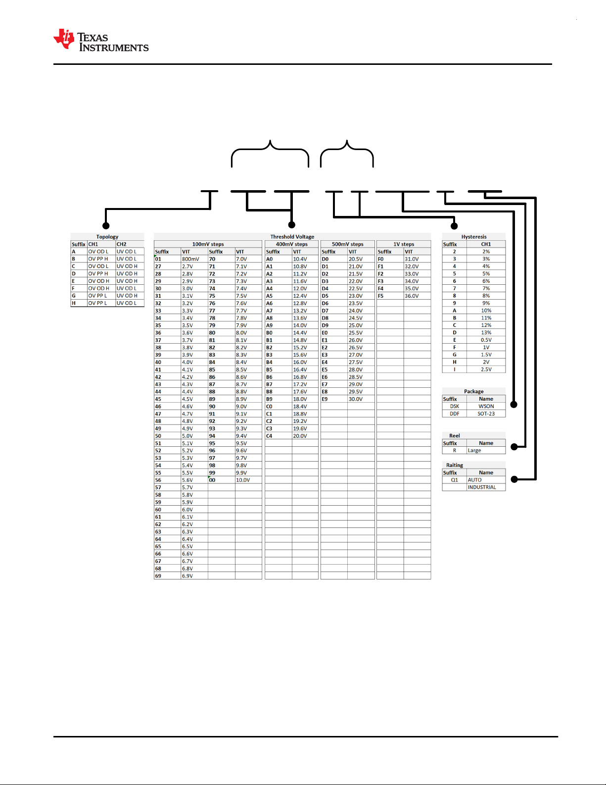
TPS37 X
XX XX
X
X
XXX R -Q1
CH 1
Voltage Threshold
CH 2 CH 1
CH 2
Hysteresis
www.ti.com
ADVANCE INFORMATION
5 Device Comparison
Contact TI sales representatives or consult TI's E2E forum for details and availability; minimum order quantities
may apply.
SNVSBD9A – AUGUST 2020 – REVISED JANUARY 2021
TPS37X-Q1
1. Sense logic: OV = Over-Voltage; UV = Under-Voltage
2. Reset topology: PP = Push-Pull; OD = Open-Drain
3. Reset logic: L = Active-Low; H = Active-High
4. A to I hysteresis options are only available for 2.9 V to 9 V threshold options
Copyright © 2021 Texas Instruments Incorporated
Product Folder Links: TPS37X-Q1
Submit Document Feedback
3
1
2
3
4
5
10
9
8
7
6
VDD
SENSE1
SENSE2
GND
CTR2/MR
RESET1_OVOD
RESET2_UVOD CTR1/MR
CTS1
CTS2
NC
(No Internal Connection)
1
2
3
4
5
10
9
8
7
6
VDD
SENSE1
SENSE2
GND
CTR2/MR
RESET1_OVPP
RESET2_UVOD CTR1/MR
CTS1
CTS2
NC
(No Internal Connection)
1
2
3
4
5
10
9
8
7
6
VDD
SENSE1
SENSE2
GND
CTR2/MR
RESET1_OVOD
RESET2_UVOD CTR1/MR
CTS1
CTS2
NC
(No Internal Connection)
1
2
3
4
5
10
9
8
7
6
VDD
SENSE1
SENSE2
GND
CTR2/MR
RESET1_OVPP
CTS1
CTS2
NC
(No Internal Connection)
1
2
3
4
5
10
9
8
7
6
VDD
SENSE1
SENSE2
GND
CTR2/MR
CTS1
CTS2
NC
(No Internal Connection)
1
2
3
4
5
10
9
8
7
6
VDD
SENSE1
SENSE2
GND
CTR2/MR
RESET1_OVOD
RESET2_UVOD CTR1/MR
CTS1
CTS2
NC
(No Internal Connection)
1
2
3
4
5
10
9
8
7
6
VDD
SENSE1
SENSE2
GND
CTR2/MR
RESET1_OVPP
CTS1
CTS2
NC
(No Internal Connection)
1
2
3
4
5
10
9
8
7
6
VDD
SENSE1
SENSE2
GND
CTR2/MR
RESET1_OVPP
RESET2_UVOD CTR1/MR
CTS1
CTS2
NC
(No Internal Connection)
TPS37X-Q1
ADVANCE INFORMATION
SNVSBD9A – AUGUST 2020 – REVISED JANUARY 2021
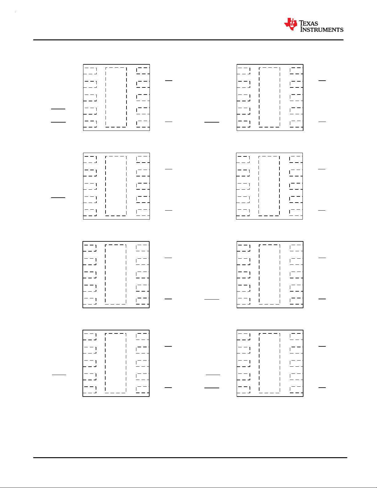
6 Pin Configuration and Functions
www.ti.com
Figure 6-1. DSK Package, 10-Pin WSON, TPS37A
(Top View)
Figure 6-3. DSK Package, 10-Pin WSON, TPS37C
(Top View)
Figure 6-5. DSK Package, 10-Pin WSON, TPS37E
(Top View)
Figure 6-2. DSK Package, 10-Pin WSON, TPS37B
(Top View)
Figure 6-4. DSK Package, 10-Pin WSON, TPS37D
(Top View)
Figure 6-6. DSK Package, 10-Pin WSON, TPS37F
(Top View)
Figure 6-7. DSK Package, 10-Pin WSON, TPS37G
(Top View)
4 Submit Document Feedback
Figure 6-8. DSK Package, 10-Pin WSON, TPS37H
(Top View)
Copyright © 2021 Texas Instruments Incorporated
Product Folder Links: TPS37X-Q1
ADVANCE INFORMATION
www.ti.com
SNVSBD9A – AUGUST 2020 – REVISED JANUARY 2021
Table 6-1. Pin Functions Generic
TPS37X-Q1
PIN
NAME NO.
VDD 1 I Input Supply Voltage.
SENSE1 2 I Input for the monitored supply voltage rail channel 1
SENSE2 3 I Input for the monitored supply voltage rail channel 2
RESET1/RESET1 4 O Output Reset Signal For Channel 1: See Section 14.1
RESET2/RESET2 5 O Output Reset Signal For Channel 2: See Section 14.1
CTR1/ MR 6
CTR2/ MR 9
GND 10 _ Ground
NC PAD - Not internally connected, the PAD can be connected to VDD, GND or be left floating.
CTS1 7
CTS2 8
TPS37A
RESET1_OVOD 4 O Reset output signal for Sense 1. Topology: Overvoltage, Open Drain, Active Low topology.
RESET2_UVOD 5 O Reset output signal for Sense 2. Topology: Undervoltage, Open Drain, Active Low topology.
TPS37B
RESET1_OVPP 4 O Reset output signal for Sense 1. Topology: Overvoltage, Push Pull, Active High topology.
RESET2_UVOD 5 O Reset output signal for Sense 2. Topology: Undervoltage, Open Drain, Active Low topology.
TPS37C
RESET1_OVOD 4 O Reset output signal for Sense 1. Topology: Overvoltage, Open Drain, Active Low topology.
RESET2_UVOD 5 O Reset output signal for Sense 2. Topology: Undervoltage, Open Drain, Active High topology.
TPS37D
RESET1_OVPP 4 O Reset output signal for Sense 1. Topology: Overvoltage, Push Pull, Active High topology.
RESET2_UVOD 5 O Reset output signal for Sense 2. Topology: Undervoltage, Open Drain, Active High topology.
TPS37E
RESET1_OVOD 4 O Reset output signal for Sense 1. Topology: Overvoltage, Open Drain, Active High topology.
RESET2_UVOD 5 O Reset output signal for Sense 2. Topology: Undervoltage, Open Drain, Active High topology.
TPS37F
RESET1_OVOD 4 O Reset output signal for Sense 1. Topology: Overvoltage, Open Drain, Active High topology.
RESET2_UVPP 5 O Reset output signal for Sense 2. Topology: Undervoltage, Push Pull, Active Low topology.
TPS37G
RESET1_OVPP 4 O Reset output signal for Sense 1. Topology: Overvoltage, Push Pull, Active Low topology.
RESET2_UVOD 5 O Reset output signal for Sense 2. Topology: Undervoltage, Open Drain, Active High topology.
TPS37H
RESET1_OVPP 4 O Reset output signal for Sense 1. Topology: Overvoltage, Push Pull, Active Low topology.
RESET2_UVOD 5 O Reset output signal for Sense 2. Topology: Overvoltage, Open Drain, Active Low topology.
I/O DESCRIPTION
_ Capacitor Time Delay Reset 1: User-programmable reset release delay for Reset 1. Connect an
external capacitor for adjustable time delay or leave floating for fastest delay.
Manual Reset: If this pin is driven low the RESET1 output will reset, leave pin floating or
connected to a cap to release reset. This pin should not be driven high.
_ Capacitor Time Delay Reset 2: User-programmable reset release delay for Reset 2. Connect an
external capacitor for adjustable time delay or leave floating for fastest delay.
Manual Reset: If this pin is driven low the RESET2 output will reset, leave pin floating or
connected to a cap to release reset. This pin should not be driven high.
_ Capacitor Time Delay Sense 1: User-programmable sense delay for Sense 1. Connect an
external capacitor for adjustable time delay or leave floating for fastest delay.
_ Capacitor Time Delay Sense 2: User-programmable sense delay for Sense 2. Connect an
external capacitor for adjustable time delay or leave floating for fastest delay.
Copyright © 2021 Texas Instruments Incorporated
Product Folder Links: TPS37X-Q1
Submit Document Feedback
5
ADVANCE INFORMATION
TPS37X-Q1
SNVSBD9A – AUGUST 2020 – REVISED JANUARY 2021
www.ti.com
7 Specifications
7.1 Absolute Maximum Ratings
over operating free-air temperature range, unless otherwise noted
Voltage VDD, V
Voltage V
Current I
Temperature
Temperature
Temperature
(2)
(2)
(2)
SENSE1,VSENSE2
, V
CTS2
, I
RESET2
, V
CTS1
RESET1
Operating junction temperature, T
Operating Ambient temperature, T
Storage, T
stg
(1) Stresses beyond those listed under Absolute Maximum Ratings may cause permanent damage to the device. These are stress ratings
only, which do not imply functional operation of the device at these or any other conditions beyond those indicated under
Recommended Operating Conditions. Exposure to absolute-maximum-rated conditions for extended periods may affect device
reliability.
(2) As a result of the low dissipated power in this device, it is assumed that TJ = TA.
CTR1
, I
RESET1
, V
, V
CTR2
, I
RESET1
RESET2
, V
7.2 ESD Ratings
Human body model (HBM), per AEC Q100-002
V
(1) AEC Q100-002 indicates that HBM stressing shall be in accordance with the ANSI/ESDA/JEDEC JS-001 specification.
Electrostatic discharge
(ESD)
Charged device model (CDM), per
AEC Q100-011
RESET2
J
A
(1)
, V
RESET1
, V
RESET2
MIN MAX UNIT
–0.3 70
–0.3 6
10 mA
–40 150 °C
–40 150 °C
–65 150 °C
VALUE UNIT
(1)
±2000
±750
V
7.3 Recommended Operating Conditions
over operating free-air temperature range (unless otherwise noted)
MIN NOM MAX UNIT
Voltage V
Voltage V
Voltage V
Current I
T
J
DD
SENSE1,VSENSE2
, V
CTS1
CTS2
, I
RESET1
RESET2
, V
, V
CTR1
, I
RESET1
RESET1
, V
CTR2
, I
, V
RESET2
RESET2
, V
RESET1
, V
RESET2
Junction temperature (free air temperature) –40 125 °C
2.7 65 V
0 65 V
0 5.5 V
0 ±5 mA
7.4 Thermal Information
(1)
R
θJA
R
θJC(top)
R
θJB
ψ
JT
ψ
JB
R
θJC(bot)
THERMAL METRIC
Junction-to-ambient thermal resistance 87.4 °C/W
Junction-to-case (top) thermal resistance 76.3 °C/W
Junction-to-board thermal resistance 54.2 °C/W
Junction-to-top characterization parameter 4.8 °C/W
Junction-to-board characterization parameter 54.2 °C/W
Junction-to-case (bottom) thermal resistance 34.8 °C/W
(1) For more information about traditional and new thermal metrics, see the Semiconductor and IC Package Thermal Metrics application
report.
DSK
10-PIN
UNIT
6 Submit Document Feedback
Copyright © 2021 Texas Instruments Incorporated
Product Folder Links: TPS37X-Q1

ADVANCE INFORMATION
www.ti.com
SNVSBD9A – AUGUST 2020 – REVISED JANUARY 2021
7.5 Electrical Characteristics
TPS37X-Q1
At V
(R
PULLUP
DD (MIN)
≤ VDD ≤ V
DD (MAX)
, CTR1 /
) = 10 kΩ, Output reset Pullup Voltage (V
free-air temperature range – 40°C to 125°C, unless otherwise noted. Typical values are at TJ = 25°C and VDD = 16 V and
VIT = 6.5 V (VIT refers to V
PARAMETER TEST CONDITIONS MIN TYP MAX UNIT
VDD
V
DD
(2)
UVLO
V
POR
V
POR
I
DD
SENSE (Input)
I
SENSE
I
SENSE
I
SENSE
I
SENSE
V
ITN
V
ITP
V
HYS
RESET (output)
I
lkg(OD)
(4)
V
OL
V
OH_DO
(4)
V
OH
Supply Voltage 2.7 65 V
Under Voltage Lockout V
Power on Reset Voltage
RESET, Active Low
(Open-Drain, Push-Pull )
Power on Reset Voltage
RESET, Active High
(Push-Pull )
Supply current into VDD pin
Input current
(SENSE1, SENSE2)
Input current
(SENSE1, SENSE2)
Input current
(SENSE1, SENSE2)
Input current
(SENSE1, SENSE2)
Input Threshold Negative
(Under-Voltage)
Input Threshold Positive
(Over-Voltage)
Hysteresis Accuracy
Open-Drain leakage
(RESET1, RESET2)
Low level output voltage
High level output voltage
dropout
(VDD - V
(Push-Pull only)
High level output voltage
(Push-Pull only)
OH
= V
ITN
OH_DO
or V
MR = CTR2 / MR = CTS1 = CTS2 = Open, Output reset Pullup Resistor
) = 5.5 V, output reset load (C
PULLUP
).
ITP
Falling below V
(5)
(5)
DD
V
OL(max)
I
OUT (Sink)
V
OH(min)
I
OUT (Source)
= 300 mV
= 15 µA
= 0.8 x V
= 15 µA
DD (MIN)
DD
VIT = 800 mV
V
DD (MIN)
≤ VDD ≤ V
DD (MAX)
VIT = 2.7 V to 36 V
V
DD (MIN)
≤ VDD ≤ V
DD (MAX)
VIT = 800 mV 100 nA
VIT < 10 V
10 V < VIT < 26 V
VIT > 26 V
VIT = 2.7 V to 36 V -1.5 1.5 %
VIT = 800 mV
(3)
0.792 0.800 0.808 V
VIT = 2.7 V to 36 V -1.5 1.5 %
VIT = 800 mV
(3)
0.792 0.800 0.808 V
VIT = 0.8 V and 2.7 V to 36 V
V
Range = 2% to 13%
HYS
-1.5 1.5 %
(1% step)
(1)
VIT = 2.7 V to 8 V
V
= 0.5 V, 1 V, 1.5 V, 2 V,
HYS
2.5 V
VIT-V
V
V
V
V
RESET
< V
ITN
RESET
< V
ITN
≥ 2.4 V
HYS
= 5.5 V
SENSE
= 65 V
SENSE
< V
< V
-1.5 1.5 %
ITP
ITP
2.7 V ≤ VDD ≤ 65 V
I
= 5 mA
RESET
)
2.7 V ≤ VDD ≤ 65 V
I
= 500 uA
RESET
2.7 V ≤ VDD ≤ 65 V
I
= 5 mA
RESET
0.8V
DD
) = 10 pF and over the operating
LOAD
1 2.6 µA
1 2 µA
2.7 V
1.4 V
1.4 V
0.8 uA
1.2 uA
2 uA
300 nA
300 nA
300 mV
43 mV
V
Copyright © 2021 Texas Instruments Incorporated
Product Folder Links: TPS37X-Q1
Submit Document Feedback
7
ADVANCE INFORMATION
TPS37X-Q1
SNVSBD9A – AUGUST 2020 – REVISED JANUARY 2021
www.ti.com
7.5 Electrical Characteristics (continued)
At V
(R
PULLUP
DD (MIN)
≤ VDD ≤ V
DD (MAX)
, CTR1 /
) = 10 kΩ, Output reset Pullup Voltage (V
free-air temperature range – 40°C to 125°C, unless otherwise noted. Typical values are at TJ = 25°C and VDD = 16 V and
VIT = 6.5 V (VIT refers to V
PARAMETER TEST CONDITIONS MIN TYP MAX UNIT
Capacitor Timing (CTS, CTR)
R
CTR
R
CTS
Manual Reset (MR)
V
MR_IH
V
MR_IH
V
MR_IL
V
MR_IL
(1) Hysteresis is with respect to V
(2) When VDD voltage falls below UVLO, reset is asserted for Output 1 and Output 2. VDD slew rate ≤ 100mV/µs
(3) For adjustable voltage guidelines and resistor selection refer to Adjustable Voltage Thresholds in Application and Implementation
section
(4) For VOH and VOL relation to output variants refer to Timing Figures after the Timing Requirement Table
(5) V
POR
Internal resistance
(CTR1 / MR , CTR2 / MR )
Internal resistance
(C
TS1, CTS2
CTR1 / MR and
CTR2 / MR pin
logic high input
CTR1 / MR and
CTR2 / MR pin
logic high input
CTR1 / MR and
CTR2 / MR pin
logic low input
CTR1 / MR and
CTR2 / MR pin
logic low input
is the minimum VDD voltage for a controlled output state. Below VPOR, the output cannot be determined. VDD dv/dt ≤ 100mV/µs
)
ITN
or V
MR = CTR2 / MR = CTS1 = CTS2 = Open, Output reset Pullup Resistor
ITP
).
ITP
and V
) = 5.5 V, output reset load (C
PULLUP
877 1000 1147 Kohms
88 100 122 Kohms
VDD = 2.7 V 2000 mV
VDD = 65 V 2500 mV
VDD = 2.7 V 1300 mV
VDD = 65 V 1300 mV
voltage threshold. V
ITN
has negative hysteresis and V
ITP
) = 10 pF and over the operating
LOAD
has positive hysteresis.
ITN
8 Submit Document Feedback
Copyright © 2021 Texas Instruments Incorporated
Product Folder Links: TPS37X-Q1
www.ti.com
ADVANCE INFORMATION
SNVSBD9A – AUGUST 2020 – REVISED JANUARY 2021
TPS37X-Q1
7.6 Timing Requirements
At V
DD_(MIN)
10 kΩ, Output reset Pullup Voltage (V
≤ VDD ≤ VDD_
, CTR1/MR = CTR2/MR = CTS1 = CTS2 = Open
(MAX)
) = 5.5V, output reset load (C
PULLUP
us, over the operating free-air temperature range – 40°C to 125°C, unless otherwise noted. Typical values are at TJ = 25°C
and VDD=16 V and VIT = 6.5 V (VIT refers to either V
PARAMETER TEST CONDITIONS MIN TYP MAX UNIT
Common timing parameters
VIT = 2.7 V to 36 V
C
= C
= C
= C
= C
TR1
TR2
TR2
TS2
TS2
= C
= C
= Open
= Open
= Open
= Open
TR2
TR1
t
CTR
Reset release time delay
(CTR1/MR, CTR2/MR)
20% Overdrive from Hysteresis
(3)
VIT = 800 mV
C
TR1
20% Overdrive from Hysteresis
VIT = 2.7 V to 36 V
C
TS1
t
CTS
Sense detect time delay
(CTS1, CTS2)
(4)
20% Overdrive from V
VIT = 800 mV
C
TS1
20% Overdrive from V
C
t
SD
(1) C
Startup Delay
= Reset delay channel 1, C
TR1
C
= Sense delay channel 1, C
TS1
(2)
TR1/MR
= Reset delay channel 2,
TR2
= Sense delay channel 2
TS2
(2) During the power-on sequence,VDD mustbe at or above VDD (MIN) for at least t
V
.
SENSE
t
time includes the propagation delay (C
SD
(3) CTR Reset detect time delay:
OVER-voltage active-LOW output is measure from V
UNDER-voltage active-LOW output is measure from V
OVER-voltage active-HIGH output is measure from V
UNDER-voltage active-HIGH output is measure from V
(4) CTS Sense detect time delay:
Active-low output is measure from VIT to VOL (or V
Active-high output is measured from VIT to VOH
VIT refers to either V
ITN
or V
ITP
or V
ITN
).
ITP
IT
IT
= Open
= Open). Capaicitor in C
TR2
to V
ITP - HYS
ITP - HYS
Pullup
ITN + HYS
ITN + HYS
)
to V
to V
to V
OH
OH
OL
OL
(1)
, Output reset Pullup Resistor (R
) = 10 pF, VDD and SENSE slew rate = 1V/
LOAD
100 us
40 us
34 90 us
8 11 us
before the output is in the correct state based on
SD
or C
TR1
will add time to t
TR2
SD.
PULLUP
2 ms
) =
Copyright © 2021 Texas Instruments Incorporated
Product Folder Links: TPS37X-Q1
Submit Document Feedback
9
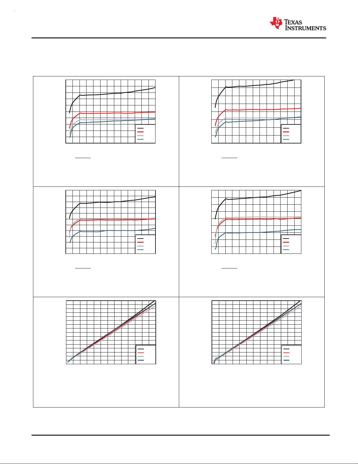
Supply Voltage (V)
Quiescent Current (µA)
0 5 10 15 20 25 30 35 40 45 50 55 60 65
0.5
0.55
0.6
0.65
0.7
0.75
0.8
0.85
0.9
0.95
1
IqNO
125 C
25 C
85 C
-40 C
Supply Voltage (V)
Quiescent Current (µA)
0 5 10 15 20 25 30 35 40 45 50 55 60 65
0.5
0.55
0.6
0.65
0.7
0.75
0.8
0.85
0.9
IqNO
125 C
25 C
85 C
-40 C
Supply Voltage (V)
Quiescent Current (µA)
0 5 10 15 20 25 30 35 40 45 50 55 60 65
0.85
0.9
0.95
1
1.05
1.1
1.15
1.2
1.25
1.3
1.35
1.4
IqAD
125 C
25 C
85 C
-40 C
Supply Voltage (V)
Quiescent Current (µA)
0 5 10 15 20 25 30 35 40 45 50 55 60 65
0.85
0.9
0.95
1
1.05
1.1
1.15
1.2
1.25
1.3
IqAD
125 C
85 C
25 C
-40 C
Sense Voltage (V)
Sense Current (nA)
0 5 10 15 20 25 30 35 40 45 50 55 60 65
0
100
200
300
400
500
600
700
800
900
1000
1100
1200
1300
1400
1500
1600
Is2p
125 C
25 C
85 C
-40 C
Sense Voltage (V)
Sense Current (nA)
0 5 10 15 20 25 30 35 40 45 50 55 60 65
0
100
200
300
400
500
600
700
800
900
1000
1100
1200
1300
1400
1500
1600
Is65
125 C
25 C
85 C
-40 C
TPS37X-Q1
ADVANCE INFORMATION
SNVSBD9A – AUGUST 2020 – REVISED JANUARY 2021
www.ti.com
8 Typical Characteristics
Typical characteristics show the typical performance of the TPS37x device. Test conditions are TJ = 25°C,
R
= 100 kΩ, C
pull-up
= 50 pF, unless otherwise noted.
Load
RESET = high, VIT = 2.7V
Figure 8-1. Supply Voltage (VDD) vs Supply Voltage
(IDD) over Temperature
RESET = high, VIT = 0.8V
Figure 8-3. Supply Voltage (VDD) vs Supply Current
(IDD) over Temperature
RESET = low, VIT = 2.7V
Figure 8-2. Supply Voltage (VDD) vs Supply Current
(IDD) over Temperature
RESET = low, VIT = 0.8V
Figure 8-4. Supply Voltage (VDD) vs Supply Current
(IDD) over Temperature
Figure 8-5. Sense Voltage (V
Current (I
10 Submit Document Feedback
VDD = 2.7V
) over Temperature
SENSE
SENSE
) vs Sense
Figure 8-6. Sense Voltage (V
Product Folder Links: TPS37X-Q1
Current (I
VDD = 65V
) vs Sense
SENSE
) over Temperature
SENSE
Copyright © 2021 Texas Instruments Incorporated
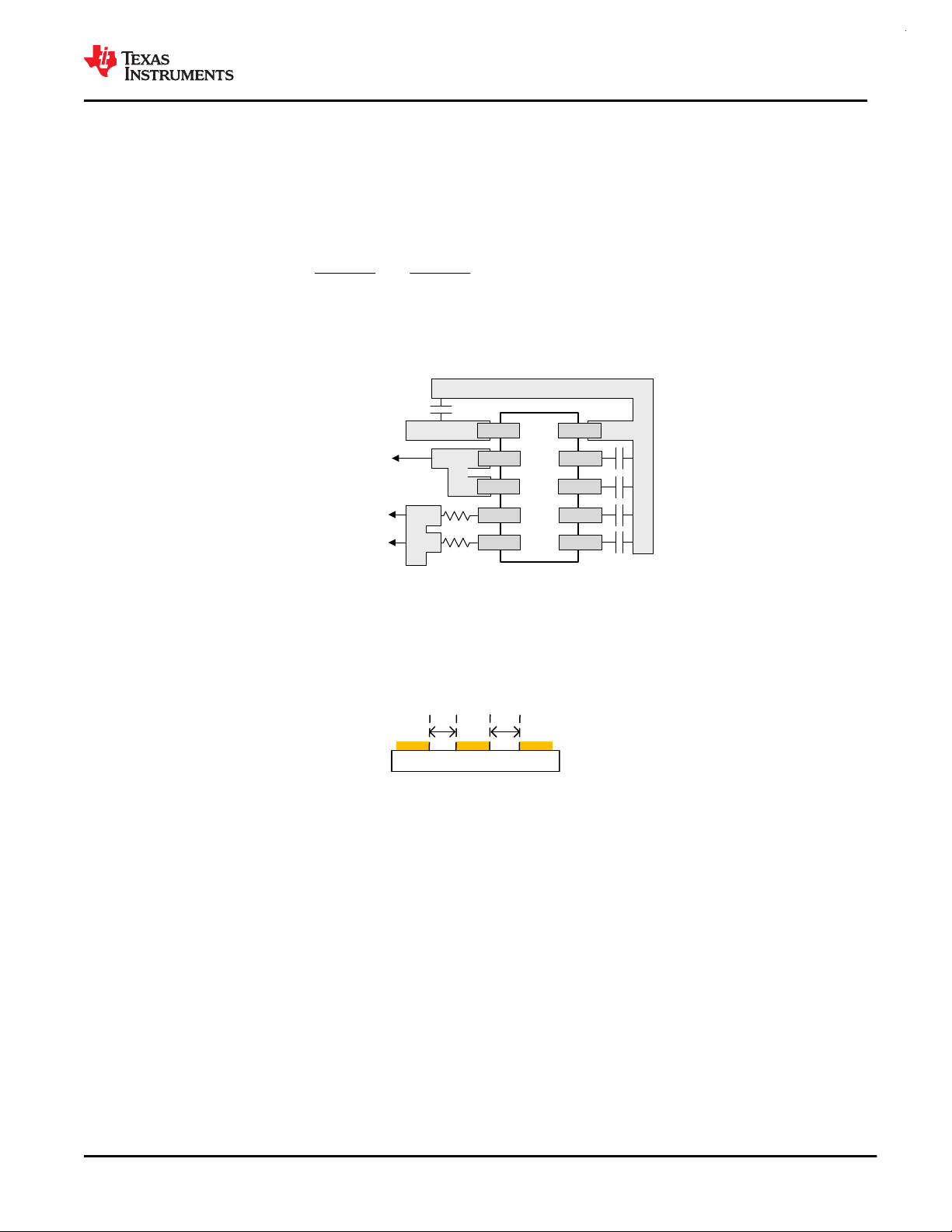
I
Q
CTS2
VDD
SubReg POR
CTR2 / MR
Sense
Delay
CTR1 / MRCTS1
V
Ref
Divider1
V
Ref
Divider2 +
-
-
+
GND
Voltage
Divider
Voltage
Divider
RESET2
Output
Logic select
(High/Low)
Output
Logic select
(High/Low)
SENSE1
SENSE2
Manual
Reset
Reset
Delay
*Device Opons
Boxes shaded in blue
See Device Nomenclature
RESET1
VDD
OV or UV
Select
BANDGAP
Sense
Delay
Manual
Reset
Reset
Delay
OV or UV
Select
www.ti.com
ADVANCE INFORMATION
SNVSBD9A – AUGUST 2020 – REVISED JANUARY 2021
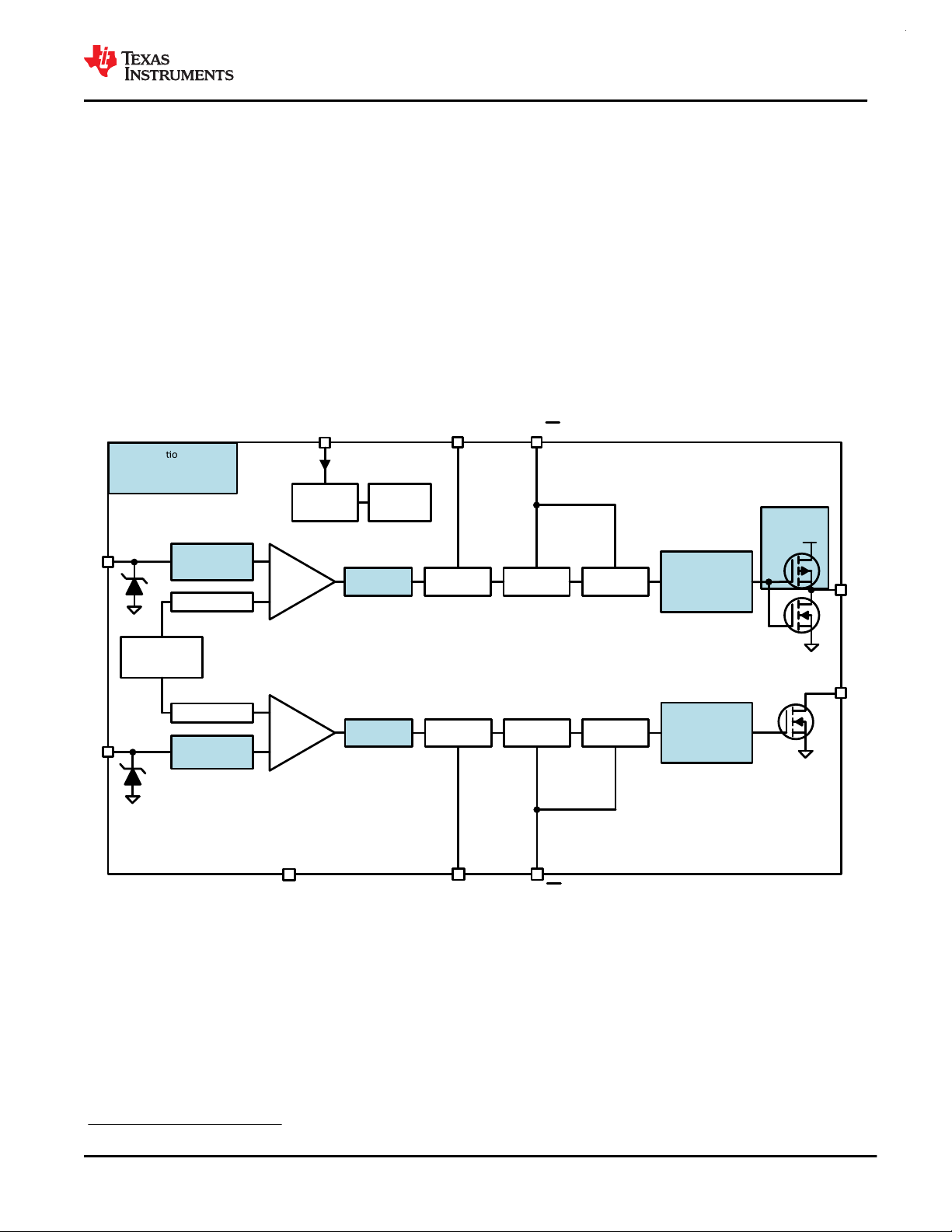
9 Detailed Description
9.1 Overview
The TPS37x is a family of high voltage and low quiescent current reset IC with fixed threshold voltage. Voltage
divider is integrated to eliminate the need for external resistors and eliminate leakage current that comes with
resistor dividers. However, it can also support external resistor if required by application, the lowest threshold
800 mV (bypass internal resistor ladder) is recommenced for external resistors use case to take advantage of
TPS37X-Q1
faster detection time and lower I
VDD, SENSE and RESET pins can support 65 V continuos operation; both VDD and SENSE voltage levels can
be independent of each other, meaning VDD pin can be connected at 2.7 V while SENSE pins are connected to
a higher voltage.
Additional features include programable sense time delay (CTS1, CTS2) and reset delay time and manual reset
(CTR1/MR, CTR2/MR).
9.2 Functional Block Diagram
SENSE
current.
1
Refer to Section 14.1 for complete list of topologies and output logic combination
Copyright © 2021 Texas Instruments Incorporated
Figure 9-1. Functional Block Diagram
Product Folder Links: TPS37X-Q1
1
Submit Document Feedback
11

SENSEx
SENSE VOLTAGE OUTSIDE OF THRESHOLD
VITN > SENSEx > VITP
Undefined
t
SD+
t
CTRx
Undefined
Output stays low since SENSE
is outside of threshold
VDD
V
DD(MIN)
UVLO
(MIN)
V
POR
V
OL
V
OL
RESETx
Active Low
RESETx
Active High
TPS37X-Q1
ADVANCE INFORMATION
SNVSBD9A – AUGUST 2020 – REVISED JANUARY 2021
www.ti.com
9.3 Feature Description
9.3.1 Input Voltage (VDD)
VDD operating voltage ranges from 2.7 V to 65 V. An input supply capacitor is not required for this device;
however, if the input supply is noisy good analog practice is to place a 0.1-µF capacitor between the VDD and
GND.
VDD needs to be at or above V
DD(MIN)
VDD voltage is independent of V
for at least the start-up time delay (tSD) for the device to be fully functional.
SENSE
and V
, meaning that VDD can be higher or lower than the other
RESET
pins.
9.3.1.1 Undervoltage Lockout (V
< VDD < UVLO)
POR
When the voltage on VDD is less than the UVLO voltage, but greater than the power-on reset voltage (V
the output pins will be in reset, regardless of the voltage at SENSE pins.
9.3.1.2 Power-On Reset (VDD < V
When the voltage on VDD is lower than the power on reset voltage (V
POR
)
), the output signal is undefined and is
POR
not to be relied upon for proper device function.
POR
),
2
Figure assume Pull-up resistor connected to VDD
12 Submit Document Feedback
Figure 9-2. Power Cycle (SENSE Outside of Nominal voltage)
Copyright © 2021 Texas Instruments Incorporated
Product Folder Links: TPS37X-Q1
2

SENSE VOLTAGE WITHING THRESHOLD
VITN < SENSEx < VITP
t
SD+
t
CTSx
Undefined
Undefined
SENSEx
VDD
V
DD(MIN)
UVLO
(MIN)
V
POR
V
OL
V
OL
RESETx
Active Low
RESETx
Active High
www.ti.com
ADVANCE INFORMATION
SNVSBD9A – AUGUST 2020 – REVISED JANUARY 2021
TPS37X-Q1
Figure 9-3. Power Cycle (SENSE Within Nominal voltage)
3
3
Figure assume Pull-up resistor connected to VDD
Copyright © 2021 Texas Instruments Incorporated
Product Folder Links: TPS37X-Q1
Submit Document Feedback
13

RESETx
V
SENSEx
VITP - VHYS
VITP
RESETx
V
SENSEx
VITP - VHYS
VITP
RESETx
V
SENSEx
VITN
VITN+VHYS
RESETx
V
SENSEx
VITN
VITN+VHYS
TPS37X-Q1
ADVANCE INFORMATION
SNVSBD9A – AUGUST 2020 – REVISED JANUARY 2021
www.ti.com
9.3.2 SENSE
The TPS37x high voltage family integrates two voltage comparators, a precision reference voltage and trimmed
resistor divider. This configuration optimizes device accuracy because all resistor tolerances are accounted for in
the accuracy and performance specifications. Device also has built-in hysteresis that provides noise immunity
and ensures stable operation.
Channels are independent of each other, meaning that SENSE1 and SENSE2 and respective outputs can be
connected to different voltage rails.
9.3.2.1 SENSE Hysteresis
Built-in hysteresis to avoid erroneous output reset release. The hysteresis is opposite to the threshold voltage;
for overvoltage options the hysteresis is subtracted from the positive threshold (V
hysteresis is added to the negative threshold (V
ITN
).
), for undervoltage options
ITP
For all the hysteresis options possible see Table 14-1.
Figure 9-4. Hysteresis (Overvoltage Active-Low)
Figure 9-6. Hysteresis (Undervoltage Active-High)
Figure 9-5. Hysteresis (Overvoltage Active-High)
Figure 9-7. Hysteresis (Undervoltage Active-Low)
14 Submit Document Feedback
Copyright © 2021 Texas Instruments Incorporated
Product Folder Links: TPS37X-Q1
www.ti.com
ADVANCE INFORMATION
SNVSBD9A – AUGUST 2020 – REVISED JANUARY 2021
TPS37X-Q1
9.3.3 Output Logic Configurations
TPS37x has two channels with separate sense pins and reset pins that can be configured independently of each
other. Channel 1 is available as Open-Drain and Push-Pull while channel 2 is only available as Open-Drain
topology.
The available output logic configuration combinations are shown in Table 9-1.
Table 9-1. TPS37x Output Logic
DESCRIPTION NOMENCLATURE VALUE
GPN TPS37 (+ topology) CHANNEL 1 CHANNEL 2
Topology (OV and UV only)
both channels are either OV or
UV
• UV = Undervoltage
• OV = Overvoltage
• PP = Push Pull
• OD = Open Drain
• L = Active low
• H = Active high
TPS37A OV OD L UV OD L
TPS37B OV PP H UV OD L
TPS37C OV OD L UV OD H
TPS37D OV PP H UV OD H
TPS37E OV OD H UV OD H
TPS37F OV PP H UV OD L
TPS37G OV OD L UV OD H
TPS37H OV OD H UV OD L
TPS37I OV PP L UV PP L
TPS37J OV PP H UV PP L
9.3.3.1 Open-Drain
Open drain output requires an external pull-up resistor to hold the voltage high to the required voltage logic.
Connect the pull-up resistor to the proper voltage rail to enable the output to be connected to other devices at
the correct interface voltage levels.
To select the right pull-up resistor consider system VOH and the (I
) current provided in the electrical
lkg
characteristics, high resistors values will have a higher voltage drop affecting the output voltage high. The opendrain output can be connected as a wired-AND logic with other open-drain signals such as another TPS37X
open-drain output pin.
9.3.3.2 Push-Pull
Push-Pull output does not require an external resistor since is the output is internally pulled-up to VDD during
VOH condition and output will be connected to GND during VOH condition.
9.3.3.3 Active-High (RESET)
RESET (active-high), denoted with no bar above the pin label. RESET remains low (VOL, deasserted) as long as
sense voltage is in normal operation within the threshold boundaries and VDD voltage is above UVLO. To assert
a reset sense pins needs to meet the condition below:
• For undervoltage variant the SENSE voltage need to cross the lower boundary (V
• For overvoltage variant the SENSE voltage needs to cross the upper boundary (V
ITN
ITP
).
).
9.3.3.4 Active-Low ( RESET)
RESET (active low) denoted with a bar above the pin label. RESET remains high voltage (VOH, deasserted)
(open drain variant VOH is measured against the pullup voltage) as long as sense voltage is in normal operation
within the threshold boundaries and VDD voltage is above UVLO. To assert a reset sense pins needs to meet
the condition below:
• For undervoltage variant the SENSE voltage need to cross the lower boundary (V
• For overvoltage variant the SENSE voltage needs to cross the upper boundary (V
ITN
ITP
).
).
Copyright © 2021 Texas Instruments Incorporated
Product Folder Links: TPS37X-Q1
Submit Document Feedback
15

TPS37X-Q1
ADVANCE INFORMATION
SNVSBD9A – AUGUST 2020 – REVISED JANUARY 2021
www.ti.com
9.3.4 User-Programmable Reset Time Delay
TPS37X has adjustable reset release time delay with external capacitors. Channel timing are independent of
each other.
• A capacitor in CTR1/MR program the reset time delay of Output 1.
• A capacitor in CTR2/MR program the reset time delay of Output 2.
• No capacitor on this pins gives the fastest reset delay time indicated in the Section 7.6.
9.3.4.1 Reset Time Delay Configuration
The time delay (t
) can be programmed by connecting a capacitor between CTR1 pin and GND, CTR2 for
CTR
channel 2. In this section CTRx represent either channel 1 or channel 2.
The relationship between external capacitor C
t
= 1.28 x R
CTRx
R
= is in kilo ohms (kOhms)
CTRx
C
CTRX_EXT
t
CTRx
= is given in microfarads (μF)
= is in milliseconds (ms)
CTRx
x C
CTRx_EXT
CTRx_EXT
and the time delay (t
) is given by Equation 1.
CTRx
(1)
The recommended maximum reset delay capacitor for the TPS37x is limited to a percentage of the period or
duration of the programmed reset time delay to ensure enough time for the capacitor to fully discharge when a
voltage fault occurs. When a voltage fault occurs, the previously charged up capacitor discharges and if the
monitored voltage returns from the fault condition before the delay capacitor discharges completely, the delay
will be shorter than expected. The capacitor will begin charging from a voltage above zero and resulting in
shorter than expected time delay. A larger delay capacitor can be used so long as the capacitor has enough time
to fully discharge during the duration of the voltage fault. To ensure the capacitor is fully discharged, the time
period or duration of the voltage fault needs to be greater than 5% of the programmed reset time delay.
9.3.5 User-Programmable Sense Delay
TPS37X has adjustable sense release time delay with external capacitors. Channel timing are independent of
each other. Sense delay is used as a de-glitcher or ignoring known transients.
• A capacitor in CTS1 program the excursion detection on sense 1.
• A capacitor in CTS2 program the excursion detection on sense 2.
• No capacitor on this pins gives the fastest detection time indicated in the Section 7.6.
9.3.5.1 Sense Time Delay Configuration
The time delay (t
) can be programmed by connecting a capacitor between CTR1 pin and GND, CTS2 for
CTS
channel 2. In this section CTRx represent either channel 1 or channel 2
The relationship between external capacitor C
t
= 1.28 x R
CTSx
R
= is in kilo ohms (kOhms)
CTSx
C
CTSX_EXT
t
CTSx
= is given in microfarads (μF)
= is in milliseconds (ms)
CTSx
x C
CTSx_EXT
CTSx_EXT
and the time delay (t
) is given by Equation 2.
CTSx
(2)
The recommended maximum sense delay capacitor for the TPS37x is limited to a percentage of the period or
duration of the programmed sense time delay to ensure enough time for the capacitor to fully discharge when a
voltage fault occurs. When a voltage fault occurs, the previously charged up capacitor discharges and if the
monitored voltage returns from the fault condition before the delay capacitor discharges completely, the delay
will be shorter than expected. The capacitor will begin charging from a voltage above zero and resulting in
shorter than expected time delay. A larger delay capacitor can be used so long as the capacitor has enough time
16 Submit Document Feedback
Product Folder Links: TPS37X-Q1
Copyright © 2021 Texas Instruments Incorporated
Low Voltage
High Voltage
Reset
Delay
CTRx
Active low
Logic
VDD
MCU
GPIO
Low or Floating
CTRx/MR
RESETx
Active-High
SENSE1
SENSE VOLTAGE WITHING THRESHOLD
VITN < SENSEx < VITP
<V
MRL
MR floating or
connected to capacitor
MR floating or
connected to capacitor
RESETx
Active-Low
www.ti.com
ADVANCE INFORMATION
SNVSBD9A – AUGUST 2020 – REVISED JANUARY 2021
to fully discharge during the duration of the voltage fault. To ensure the capacitor is fully discharged, the time
period or duration of the voltage fault needs to be greater than 10% of the programmed sense time delay.
9.3.6 Manual RESET (CTR1/ MR) and (CTR2/ MR) Input
The manual reset input allows a processor or other logic circuits to initiate a reset. In this section MR is a generic
reference to (CTR1/ MR) and (CTR2/ MR). A logic low on MR causes RESET1 to assert on reset output. After
MR is left floating, RESET1 will release the reset if the voltage at SENSE1 pin is at nominal voltage. MR should
not be driven high, this pin should be left floating or connected to a capacitor to GND, this pin can be left
unconnected if is not used.
If the logic driving the MR cannot tri-state (floating and GND) then a logic-level FET should be used as illustrated
in Figure 9-8.
TPS37X-Q1
MR SENSE ON NOMINAL VOLTAGE RESET STATUS
Low Yes Reset asserted
Floating Yes
Capacitor Yes Programable reset time delay
High Yes NOT Recommended
Copyright © 2021 Texas Instruments Incorporated
Figure 9-8. Manual Reset Implementation
Figure 9-9. Manual Rest Timing Diagram
Table 9-2. MR Functional Table
Product Folder Links: TPS37X-Q1
Fast reset release when SENSE
voltage goes back to nominal
voltage
Submit Document Feedback
17
TPS37X-Q1
ADVANCE INFORMATION
SNVSBD9A – AUGUST 2020 – REVISED JANUARY 2021
10 Device Functional Modes
Table 10-1. Undervoltage Detect Functional Mode Truth Table
SENSE
DESCRIPTION
Normal Operation SENSE > V
Undervoltage
Detection
Undervoltage
Detection
Normal Operation SENSE < V
Manual Reset SENSE > V
UVLO Engaged SENSE > V
Below V
POR
,
Undefined Output
PREVIOUS
CONDITION
SENSE > V
SENSE < V
SENSE > V
ITN(UV)
ITN(UV)
ITN(UV)
ITN(UV)
ITN(UV)
ITN(UV)
ITN(UV)
CURRENT CONDITION
SENSE > V
SENSE < V
SENSE > V
SENSE > V
SENSE > V
SENSE > V
SENSE > V
ITN(UV)
ITN(UV)
ITN(UV)
ITN(UV)
ITN(UV)
ITN(UV)
ITN(UV)
+ HYS
1. Reset time delay is ignored in the truth table
2. Open-drain active low output. External pull-up resistor to high voltage
(1)
CTR
/ MR PIN VDD PIN
Open or capacitor
connected
Open or capacitor
connected
Open or capacitor
connected
Open or capacitor
connected
Low VDD > V
Open or capacitor
connected
Open or capacitor
connected
V
POR
VDD > V
VDD > V
VDD > V
VDD > V
< VDD < V
VDD < V
DD(MIN)
DD(MIN)
DD(MIN)
DD(MIN)
DD(MIN)
DD(MIN)
POR
www.ti.com
OUTPUT
(2)
(RESET PIN)
High
Low
Low
High
Low
Low
Undefined
Table 10-2. Overvoltage Detect Functional Mode Truth Table
DESCRIPTION
PREVIOUS
CONDITION
Normal Operation SENSE < V
Undervoltage
Detection
Undervoltage
Detection
SENSE < V
SENSE > V
Normal Operation SENSE > V
Manual Reset SENSE < V
UVLO Engaged SENSE < V
Below V
Undefined Output
POR
,
SENSE < V
ITN(OV)
ITN(OV)
ITN(OV)
ITN(OV)
ITN(OV)
ITN(OV)
ITN(OV)
SENSE
CURRENT CONDITION
SENSE < V
SENSE > V
SENSE < V
SENSE < V
SENSE < V
SENSE < V
SENSE < V
ITN(OV)
ITN(OV)
ITN(OV)
ITN(OV)
ITN(OV)
ITN(OV)
ITN(OV)
- HYS
(1)
CTR
/ MR PIN VDD PIN
Open or capacitor
connected
Open or capacitor
connected
Open or capacitor
connected
Open or capacitor
connected
Low VDD > V
Open or capacitor
connected
Open or capacitor
connected
1. Reset time delay is ignored in the truth table
2. Open-drain active low output. External pull-up resistor to high voltage
VDD > V
DD(MIN)
VDD > V
DD(MIN)
VDD > V
DD(MIN)
VDD > V
DD(MIN)
DD(MIN)
V
< VDD < UVLO Low
POR
VDD < V
POR
OUTPUT
(2)
(RESET PIN)
High
Low
Low
High
Low
Undefined
18 Submit Document Feedback
Copyright © 2021 Texas Instruments Incorporated
Product Folder Links: TPS37X-Q1

www.ti.com
ADVANCE INFORMATION
SNVSBD9A – AUGUST 2020 – REVISED JANUARY 2021
TPS37X-Q1
11 Application and Implementation
Note
Information in the following applications sections is not part of the TI component specification, and TI
does not warrant its accuracy or completeness. TI’s customers are responsible for determining
suitability of components for their purposes, as well as validating and testing their design
implementation to confirm system functionality.
11.1 Adjustable Voltage Thresholds
Equation 3 illustrates an example of how to adjust the voltage threshold with external resistor dividers. The
resistors can be calculated depending on the desired voltage threshold and device part number. TI recommends
using the 0.8V voltage threshold device when using an adjustable voltage variant. This variant bypasses the
internal resistor ladder.
For example, consider a 2.0 V rail being monitored (V
R2 = 10 kΩ, V
be denoted as V
V
SENSE
= 2 V, and V
MON
, the monitored undervoltage threshold where the device will assert a reset signal.
MON-
= V
MON
SENSE
× (R2 ÷ (R1 + R2))
= 0.8 V. Using Equation 3, V
) using. Using Equation 3, R1 = 15 kΩ given that
MON
= 1.94 V when V
MON
SENSE
= V
IT-(UV)
. This can
(3)
Aside from the tolerance of the resistor divider, the SENSE pin leakage current affects the accuracy of the
resistor divider. The sense leakage, I
, is given in Section 7.5. The actual input threshold due to the leakage
SENSE
SENSE current can be calculated with Equation 4
I
VIT_Actual
= V
MON
+ R1 ((V
÷ R2) + I
REF
SENSE
)
(4)
11.2 Application Information
The following sections describe in detail how to properly use this device, depending on the requirements of the
final application.
Copyright © 2021 Texas Instruments Incorporated
Product Folder Links: TPS37X-Q1
Submit Document Feedback
19
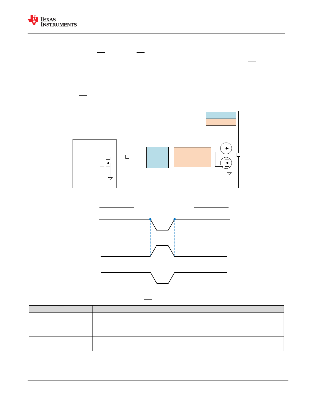
DC/DC
MCU
Low Iq, No external
resistors needed
GND
Boost
Converter
MCU Flag
Enable
Boost
SENSE1
SENSE2
RESET1
RESET2
Backup
Vbatt
VDD
GND
VDD
GPIO
TPS37X
TPS37X-Q1
ADVANCE INFORMATION
SNVSBD9A – AUGUST 2020 – REVISED JANUARY 2021
www.ti.com
11.3 Typical Application
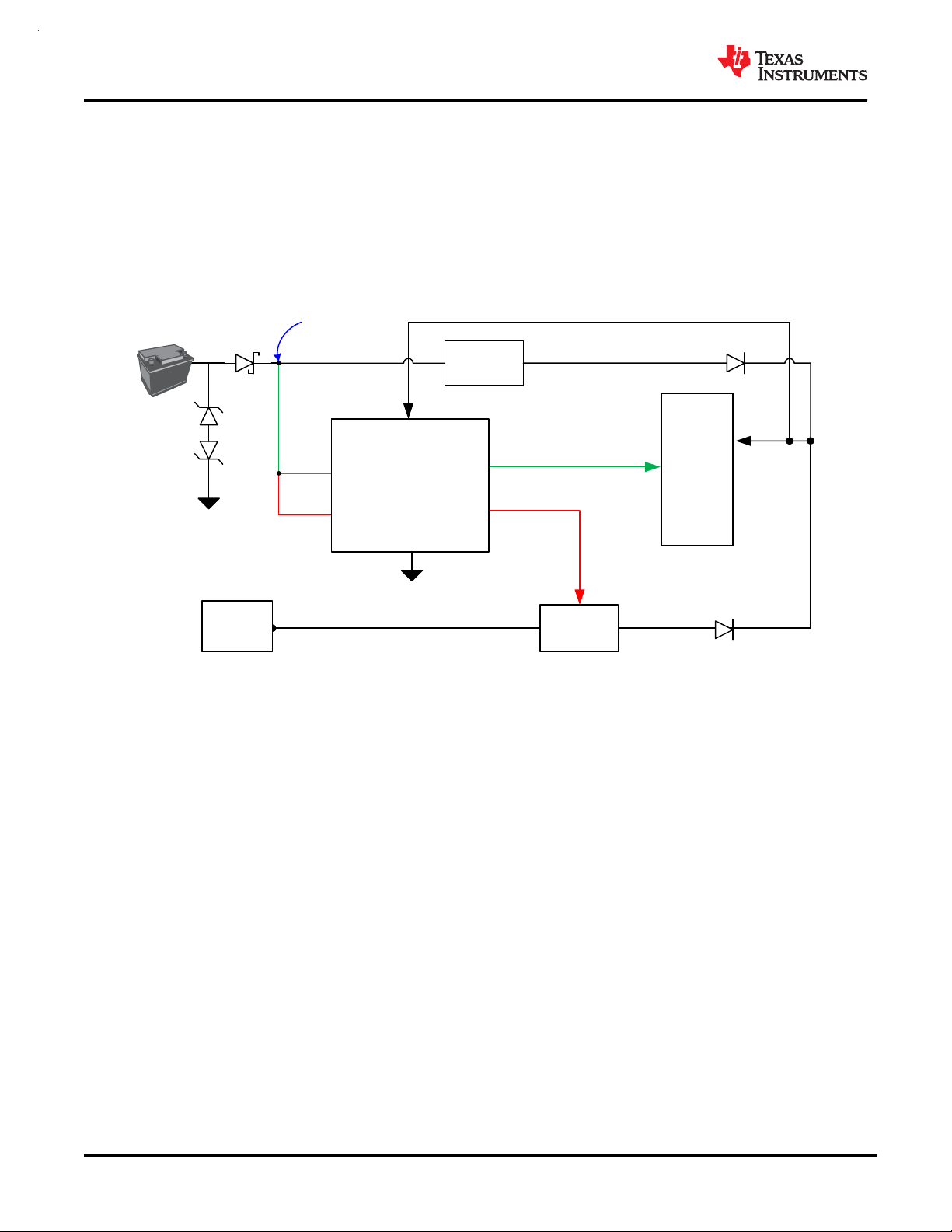
11.3.1 Design 1: Automotive Off-Battery Monitoring
The initial power stage in automotive applications starts with the 12 V battery. Variation of the battery voltage is
common between 9 V and 16 V. Furthermore, if cold-cranking and load dump conditions are considered, voltage
transients can occur as low as 3 V and as high as 42 V. In this design example, we are highlighting the ability for
low power, direct off-battery voltage supervision. Figure 11-1 illustrates an example of how the TPS37x-Q1 is
monitoring the battery voltage while being powered by it, as well. For more information, read this application
report on how to achieve low IQ voltage supervision in automotive, wide-VIN applications.
Figure 11-1. Fast Start Window Supervisor with Direct Off-Battery Monitoring
20 Submit Document Feedback
Product Folder Links: TPS37X-Q1
Copyright © 2021 Texas Instruments Incorporated
www.ti.com
ADVANCE INFORMATION
SNVSBD9A – AUGUST 2020 – REVISED JANUARY 2021
11.3.1.1 Design Requirements
This design requires voltage supervision on a 12-V power supply voltage rail with possibility of the 12-V rail rising
up as high as 42 V. The undervoltage fault occurs when the power supply voltage drops below 7.7 V.
TPS37X-Q1
PARAMETER DESIGN REQUIREMENT DESIGN RESULT
Power Rail Voltage Supervision
Maximum Input Power Operate with power supply input up to 42 V. The TPS37x-Q1 can support a VDD of up to 65 V.
Output logic voltage Open-Drain Output Topology
Maximum system current
consumption
Voltage Monitor Accuracy Maximum voltage monitor accuracy of 1.5%.
Delay when returning from fault
condition
Monitor 12-V power supply for undervoltage
condition, trigger a undervoltage fault at 7.7 V.
2 µA max when power supply is at 12 V typical
RESET delay of at least 420 ms when returning
from a undervoltage fault.
TPS37x-Q1 provides voltage monitoring with 1.5%
max accuracy with adjustable/non-adjustable
variations.
An open-drain output is recommended to provide
the correct reset signal, but a push-pull can also be
used.
TPS37x-Q1 allows for IQ to remain low with support
of up to 65 V. This allows for no external resistor
divider to be required.
The TPS37x-Q1 has 1.5% maximum voltage
monitor accuracy.
C
= .033 µF sets 422 ms delay
CTR
11.3.1.2 Detailed Design Procedure
The primary advantage of this application is being able to monitor a voltage on an automotive battery without
needing external resistors on the input. This keeps IQ low while still achieving the desired rail monitoring.
As shown in Figure 11-1, the rail monitoring can be done directly with the SENSE1 and SENSE2 inputs directly
connected to the battery rail after the protection diodes.
To use this configuration, the specific voltage threshold variation of the device must be chosen according to the
application. In this configuration, the '77' variation must be chosen for 7.7 V as shown in Table 14-2.
The device being able to handle 65 V on VDD means the monitored voltage rail can go as high as 42 V for the
application transients and not violate the recommended maximum for the supervisor as it usally would. This is
useful when monitoring a voltage rail that has a wide range that may go much higher than the nominal rail
voltage such as in this case. Good design practice recommends using a 0.1-µF capacitor on the VDD pin and
this capacitance may need to increase if using an adjustable version with a resistor divider.
Copyright © 2021 Texas Instruments Incorporated
Product Folder Links: TPS37X-Q1
Submit Document Feedback
21

TPS37X-Q1
ADVANCE INFORMATION
SNVSBD9A – AUGUST 2020 – REVISED JANUARY 2021
12 Power Supply Recommendations
www.ti.com
These devices are designed to operate from an input supply with a voltage range between 1.4 V (V
POR
) to 65 V
(max operation). Good analog design practice recommends placing a minimum 0.1-µF ceramic capacitor as
near as possible to the VDD pin.
12.1 Power Dissipation and Device Operation
The permissible power dissipation for any package is a measure of the capability of the device to pass heat from
the power source, the junctions of the IC, to the ultimate heat sink, the ambient environment. Thus, the power
dissipation is dependent on the ambient temperature and the thermal resistance across the various interfaces
between the die junction and ambient air.
The maximum continuos allowable power dissipation for the device in a given package can be calculated using
Equation 5:
P
= ((T
D-MAX
The actual power being dissipated in the device can be represented by Equation 6:
P
= VDD × IDD + p
D
p
is calculated by Equation 7 or Equation 8
RESET
p
RESET (PUSHPULL)
p
RESET (OPEN-DRAIN)
Equation 5 and Equation 6 establish the relationship between the maximum power dissipation allowed due to
thermal consideration, the voltage drop across the device, and the continuous current capability of the device.
These two equations should be used to determine the optimum operating conditions for the device in the
application.
J-MAX
– TA) / R
RESET
= VDD - V
= V
RESET
θJA
RESET
)
x I
x I
RESET
RESET
(5)
(6)
(7)
(8)
In applications where lower power dissipation (PD) and/or excellent package thermal resistance (R
present, the maximum ambient temperature (T
) may be increased.
A-MAX
θJA
) is
In applications where high power dissipation and/or poor package thermal resistance is present, the maximum
ambient temperature (T
temperature (T
application (P
J-MAX-OP
), and the junction-to ambient thermal resistance of the part/package in the application (R
D-MAX
) may have to be derated. T
A-MAX
is dependent on the maximum operating junction
A-MAX
= 125°C), the maximum allowable power dissipation in the device package in the
θJA
as given by Equation 9:
T
A-MAX
= (T
J-MAX-OP
– (R
θJA
× P
D-MAX
))
(9)
),
22 Submit Document Feedback
Copyright © 2021 Texas Instruments Incorporated
Product Folder Links: TPS37X-Q1
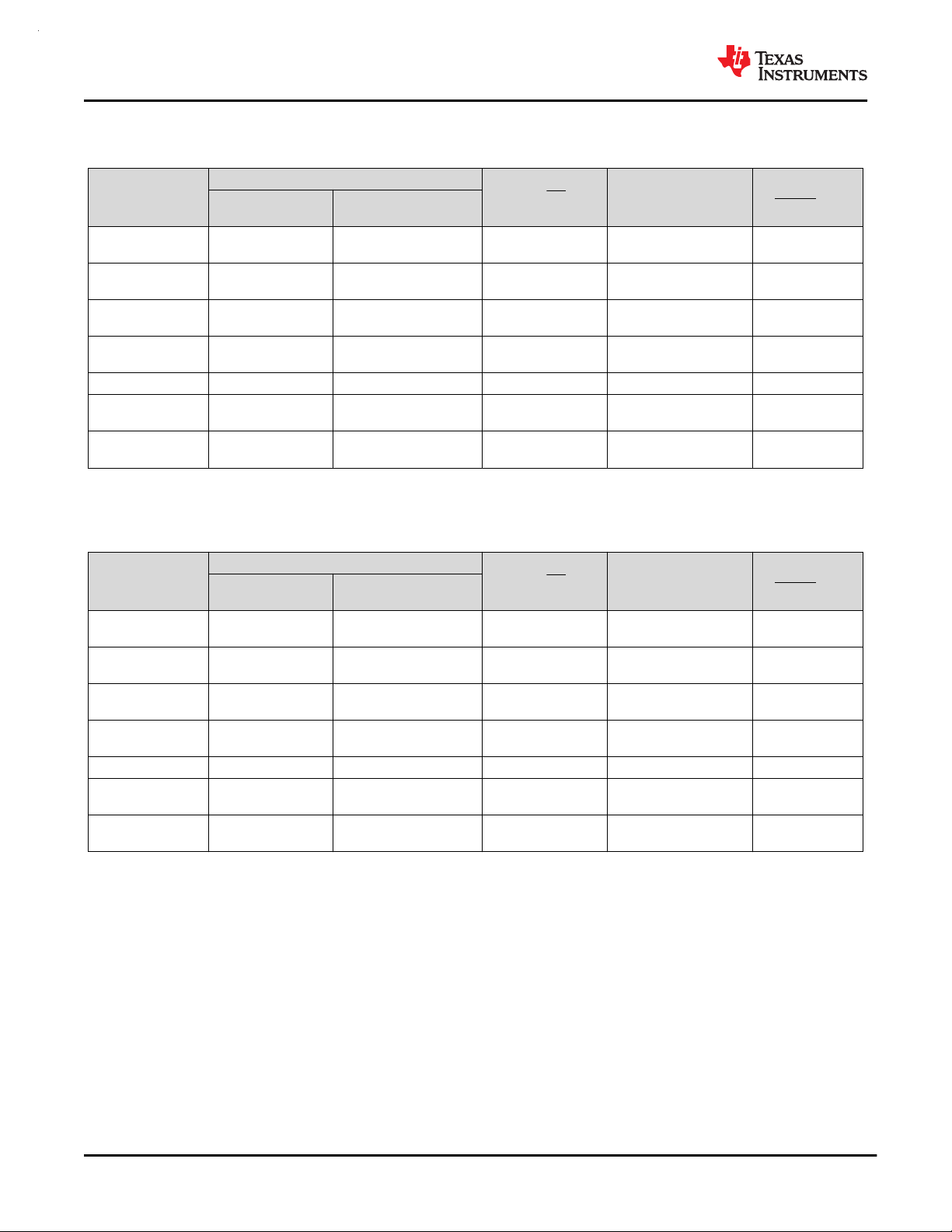
Monitored
Voltage
Overvoltage Flag
C
VDD
2 9
3 8
4 7
5 6
10 GND
R
PU2
1V
DD
R
PU1
TPS37X
V
PULL-UP
a
b
B
A
C
www.ti.com
ADVANCE INFORMATION
SNVSBD9A – AUGUST 2020 – REVISED JANUARY 2021
13 Layout
13.1 Layout Guidelines
• Make sure that the connection to the VDD pin is low impedance. Good analog design practice is to place a
greater than 0.1-µF ceramic capacitor as near as possible to the VDD pin.
• If a capacitor is used on CTS1, CTS2, CTR1, or CTR2, place these components as close as possible to the
respective pins. If the capacitor adjustable pins are left unconnected, make sure to minimize the amount of
parasitic capacitance on the pins to less than 5 pF.
TPS37X-Q1
• Place the pull-up resistors on
13.2 Layout Example
The layout example in Figure 13-1 shows how the TPS37x-Q1 is laid out on a printed circuit board (PCB) with
user-defined delays.
RESET1 and RESET2 pins as close to the pins as possible.
Figure 13-1. TPS37x-Q1 Recommended Layout
13.3 Creepage Distance
Per IEC 60664 Creepage is the shortest distance between two conductive parts or as shown in Figure 13-2 the
distance between high voltage conductive parts and grounded parts, the floating conductive part is ignored and
subtracted from the total distance.
Figure 13-2. Creepage Distance
Figure 13-2 details
• A = Left pins (high voltage)
• B = Central pad (conductive not internally connected
• C = Right pins (low voltages)
• Creepage distance = a + b
Copyright © 2021 Texas Instruments Incorporated
Product Folder Links: TPS37X-Q1
Submit Document Feedback
23
ADVANCE INFORMATION
TPS37X-Q1
SNVSBD9A – AUGUST 2020 – REVISED JANUARY 2021
www.ti.com
14 Device and Documentation Support
14.1 Device Nomenclature
Section 5 shows how to decode the function of the device based on its part number
Table 14-2 shows TPS37x possible voltage options per channel. Contact TI sales representatives or on TI's E2E
forum for details and availability of other options; minimum order quantities apply.
Table 14-1 shows TPS37x common hysteresis and voltage options.
Table 14-1. Common Hysteresis Lookup Table
TARGET
DETECT THRESHOLD TOPOLOGY RELEASE VOLTAGE (V)
18.0 V Overvoltage 17.5 V -3%
18.0 V Overvoltage 16.0 V -11%
17.0 V Overvoltage 16.5 V -3%
16.0 V Overvoltage 15.0 V -6%
15.0 V Overvoltage 14.0 V -7%
6.0 V Undervoltage 6.5 V 0.5 V
5.5 V Undervoltage 6 V 0.5 V
8 V Undervoltage 9 V 1 V
5 V Undervoltage 7.5 V 2.5 V
DEVICE ACTUAL HYSTERESIS OPTION
24 Submit Document Feedback
Copyright © 2021 Texas Instruments Incorporated
Product Folder Links: TPS37X-Q1
ADVANCE INFORMATION
www.ti.com
SNVSBD9A – AUGUST 2020 – REVISED JANUARY 2021
Table 14-2. Voltage Options
100 mV STEPS 400 mV STEPS 500 mV STEPS 1 V STEPS
NOMEN-
CLATURE
08 800 mV
27 2.7 V 71 7.1 V A1 10.8 V D1 21.0 V F1 32.0 V
28 2.8 V 72 7.2 V A2 11.2 V D2 21.5 V F2 33.0 V
29 2.9 V 73 7.3 V A3 11.6 V D3 22.0 V F3 34.0 V
30 3.0 V 74 7.4 V A4 12.0 V D4 22.5 V F4 35.0 V
31 3.1 V 75 7.5 V A5 12.4 V D5 23.0 V F5 36.0 V
32 3.2 V 76 7.6 V A6 12.8 V D6 23.5 V
33 3.3 V 77 7.7 V A7 13.2 V D7 24.0 V
34 3.4 V 78 7.8 V A8 13.6 V D8 24.5 V
35 3.5 V 79 7.9 V A9 14.0 V D9 25.0 V
36 3.6 V 80 8.0 V B0 14.4 V E0 25.5 V
37 3.7 V 81 8.1 V B1 14.8 V E1 26.0 V
38 3.8 V 82 8.2 V B2 15.2 V E2 26.5 V
39 3.9 V 83 8.3 V B3 15.6 V E3 27.0 V
40 4.0 V 84 8.4 V B4 16.0 V E4 27.5 V
41 4.1 V 85 8.5 V B5 16.4 V E5 28.0 V
42 4.2 V 86 8.6 V B6 16.8 V E6 28.5 V
43 4.3 V 87 8.7 V B7 17.2 V E7 29.0 V
44 4.4 V 88 8.8 V B8 17.6 V E8 29.5 V
45 4.5 V 89 8.9 V B9 18.0 V E9 30.0 V
46 4.6 V 90 9.0 V C0 18.4 V
47 4.7 V 91 9.1 V C1 18.8 V
48 4.8 V 92 9.2 V C2 19.2 V
49 4.9 V 93 9.3 V C3 19.6 V
50 5.0 V 94 9.4 V C4 20.0 V
51 5.1 V 95 9.5 V
52 5.2 V 96 9.6 V
53 5.3 V 97 9.7 V
54 5.4 V 98 9.8 V
55 5.5 V 99 9.9 V
56 5.6 V 00 10.0 V
57 5.7 V
58 5.8 V
59 5.9 V
60 6.0 V
61 6.1 V
62 6.2 V
63 6.3 V
64 6.4 V
65 6.5 V
66 6.6 V
67 6.7 V
VOLTAGE
OPTIONS
(divider
bypass)
NOMEN-
CLATURE
70 7.0 V A0 10.4 V D0 20.5 V F0 31.0 V
VOLTAGE
OPTIONS
NOMEN-
CLATURE
VOLTAGE
OPTIONS
NOMEN-
CLATURE
VOLTAGE
OPTIONS
NOMEN-
CLATURE
TPS37X-Q1
VOLTAGE
OPTIONS
Copyright © 2021 Texas Instruments Incorporated
Product Folder Links: TPS37X-Q1
Submit Document Feedback
25

ADVANCE INFORMATION
TPS37X-Q1
SNVSBD9A – AUGUST 2020 – REVISED JANUARY 2021
www.ti.com
Table 14-2. Voltage Options (continued)
100 mV STEPS 400 mV STEPS 500 mV STEPS 1 V STEPS
NOMEN-
CLATURE
68 6.8 V
69 6.9 V
VOLTAGE
OPTIONS
NOMEN-
CLATURE
VOLTAGE
OPTIONS
NOMEN-
CLATURE
VOLTAGE
OPTIONS
NOMEN-
CLATURE
VOLTAGE
OPTIONS
NOMEN-
CLATURE
VOLTAGE
OPTIONS
14.2 Support Resources
TI E2E™ support forums are an engineer's go-to source for fast, verified answers and design help — straight
from the experts. Search existing answers or ask your own question to get the quick design help you need.
Linked content is provided "AS IS" by the respective contributors. They do not constitute TI specifications and do
not necessarily reflect TI's views; see TI's Terms of Use.
14.3 Trademarks
TI E2E™ is a trademark of Texas Instruments.
All trademarks are the property of their respective owners.
14.4 Electrostatic Discharge Caution
This integrated circuit can be damaged by ESD. Texas Instruments recommends that all integrated circuits be handled
with appropriate precautions. Failure to observe proper handling and installation procedures can cause damage.
ESD damage can range from subtle performance degradation to complete device failure. Precision integrated circuits may
be more susceptible to damage because very small parametric changes could cause the device not to meet its published
specifications.
14.5 Glossary
TI Glossary This glossary lists and explains terms, acronyms, and definitions.
15 Mechanical, Packaging, and Orderable Information
The following pages include mechanical, packaging, and orderable information. This information is the most
current data available for the designated devices. This data is subject to change without notice and revision of
this document. For browser-based versions of this data sheet, refer to the left-hand navigation.
26 Submit Document Feedback
Copyright © 2021 Texas Instruments Incorporated
Product Folder Links: TPS37X-Q1
www.ti.com
ADVANCE INFORMATION
SNVSBD9A – AUGUST 2020 – REVISED JANUARY 2021
TPS37X-Q1
Copyright © 2021 Texas Instruments Incorporated
Product Folder Links: TPS37X-Q1
Submit Document Feedback
27

TPS37X-Q1
ADVANCE INFORMATION
SNVSBD9A – AUGUST 2020 – REVISED JANUARY 2021
www.ti.com
28 Submit Document Feedback
Copyright © 2021 Texas Instruments Incorporated
Product Folder Links: TPS37X-Q1

www.ti.com
ADVANCE INFORMATION
SNVSBD9A – AUGUST 2020 – REVISED JANUARY 2021
TPS37X-Q1
Copyright © 2021 Texas Instruments Incorporated
Product Folder Links: TPS37X-Q1
Submit Document Feedback
29

PACKAGE OPTION ADDENDUM
www.ti.com
PACKAGING INFORMATION
Orderable Device Status
PS37A010122DSKRQ1 ACTIVE SON DSK 10 3000 Non-RoHS &
(1)
The marketing status values are defined as follows:
ACTIVE: Product device recommended for new designs.
LIFEBUY: TI has announced that the device will be discontinued, and a lifetime-buy period is in effect.
NRND: Not recommended for new designs. Device is in production to support existing customers, but TI does not recommend using this part in a new design.
PREVIEW: Device has been announced but is not in production. Samples may or may not be available.
OBSOLETE: TI has discontinued the production of the device.
Package Type Package
(1)
Drawing
Pins Package
Qty
Eco Plan
(2)
Non-Green
Lead finish/
Ball material
(6)
Call TI Call TI -40 to 125
MSL Peak Temp
(3)
Op Temp (°C) Device Marking
(4/5)
(2)
RoHS: TI defines "RoHS" to mean semiconductor products that are compliant with the current EU RoHS requirements for all 10 RoHS substances, including the requirement that RoHS substance
do not exceed 0.1% by weight in homogeneous materials. Where designed to be soldered at high temperatures, "RoHS" products are suitable for use in specified lead-free processes. TI may
reference these types of products as "Pb-Free".
RoHS Exempt: TI defines "RoHS Exempt" to mean products that contain lead but are compliant with EU RoHS pursuant to a specific EU RoHS exemption.
Green: TI defines "Green" to mean the content of Chlorine (Cl) and Bromine (Br) based flame retardants meet JS709B low halogen requirements of <=1000ppm threshold. Antimony trioxide based
flame retardants must also meet the <=1000ppm threshold requirement.
(3)
MSL, Peak Temp. - The Moisture Sensitivity Level rating according to the JEDEC industry standard classifications, and peak solder temperature.
(4)
There may be additional marking, which relates to the logo, the lot trace code information, or the environmental category on the device.
(5)
Multiple Device Markings will be inside parentheses. Only one Device Marking contained in parentheses and separated by a "~" will appear on a device. If a line is indented then it is a continuation
of the previous line and the two combined represent the entire Device Marking for that device.
(6)
Lead finish/Ball material - Orderable Devices may have multiple material finish options. Finish options are separated by a vertical ruled line. Lead finish/Ball material values may wrap to two
lines if the finish value exceeds the maximum column width.
Important Information and Disclaimer:The information provided on this page represents TI's knowledge and belief as of the date that it is provided. TI bases its knowledge and belief on information
provided by third parties, and makes no representation or warranty as to the accuracy of such information. Efforts are underway to better integrate information from third parties. TI has taken and
continues to take reasonable steps to provide representative and accurate information but may not have conducted destructive testing or chemical analysis on incoming materials and chemicals.
TI and TI suppliers consider certain information to be proprietary, and thus CAS numbers and other limited information may not be available for release.
In no event shall TI's liability arising out of such information exceed the total purchase price of the TI part(s) at issue in this document sold by TI to Customer on an annual basis.
9-Mar-2021
Samples
Addendum-Page 1

GENERIC PACKAGE VIEW
DSK 10
2.5 x 2.5 mm, 0.5 mm pitch
WSON - 0.8 mm max height
PLASTIC SMALL OUTLINE - NO LEAD
Images above are just a representation of the package family, actual package may vary.
Refer to the product data sheet for package details.
4225304/A

IMPORTANT NOTICE AND DISCLAIMER
TI PROVIDES TECHNICAL AND RELIABILITY DATA (INCLUDING DATASHEETS), DESIGN RESOURCES (INCLUDING REFERENCE
DESIGNS), APPLICATION OR OTHER DESIGN ADVICE, WEB TOOLS, SAFETY INFORMATION, AND OTHER RESOURCES “AS IS”
AND WITH ALL FAULTS, AND DISCLAIMS ALL WARRANTIES, EXPRESS AND IMPLIED, INCLUDING WITHOUT LIMITATION ANY
IMPLIED WARRANTIES OF MERCHANTABILITY, FITNESS FOR A PARTICULAR PURPOSE OR NON-INFRINGEMENT OF THIRD
PARTY INTELLECTUAL PROPERTY RIGHTS.
These resources are intended for skilled developers designing with TI products. You are solely responsible for (1) selecting the appropriate
TI products for your application, (2) designing, validating and testing your application, and (3) ensuring your application meets applicable
standards, and any other safety, security, or other requirements. These resources are subject to change without notice. TI grants you
permission to use these resources only for development of an application that uses the TI products described in the resource. Other
reproduction and display of these resources is prohibited. No license is granted to any other TI intellectual property right or to any third party
intellectual property right. TI disclaims responsibility for, and you will fully indemnify TI and its representatives against, any claims, damages,
costs, losses, and liabilities arising out of your use of these resources.
TI’s products are provided subject to TI’s Terms of Sale (https:www.ti.com/legal/termsofsale.html) or other applicable terms available either
on ti.com or provided in conjunction with such TI products. TI’s provision of these resources does not expand or otherwise alter TI’s
applicable warranties or warranty disclaimers for TI products.IMPORTANT NOTICE
Mailing Address: Texas Instruments, Post Office Box 655303, Dallas, Texas 75265
Copyright © 2021, Texas Instruments Incorporated
 Loading...