

Datasheet TPS3705-30, TPS3705-33, TPS3705-50, TPS3707-25, TPS3707-30 Datasheet (TEXAS INSTRUMENTS)
...Page 1
TPS3705-30, TPS3705-33, TPS3705-50
TPS3707-25, TPS3707-30, TPS3707-33, TPS3707-50
PROCESSOR SUPERVISORY CIRCUITS WITH POWER-FAIL
SLVS184B – NOVEMBER 1998 – REVISED JANUAR Y 1999
features
D
Power-On Reset Generator with Fixed
Delay Time of 200 ms, no External
Capacitor Needed
D
Precision Supply Voltage Monitor 2.5 V, 3 V,
3.3 V, and 5 V
D
Pin-For-Pin Compatible with the MAX705
through MAX708 Series
D
Integrated Watchdog Timer (TPS3705 only)
D
Voltage Monitor for Power-Fail or
Low-Battery Warning
D
Maximum Supply Current of 50 µA
D
MSOP-8 and SO-8 Packages
D
T emperature Range...–40°C to 85°C
typical applications
D
Designs Using DSPs, Microcontrollers or
Microprocessors
D
Industrial Equipment
D
Programmable Controls
D
Automotive Systems
D
Portable/Battery Powered Equipment
D
Intelligent Instruments
D
Wireless Communication Systems
D
Notebook/Desktop Computers
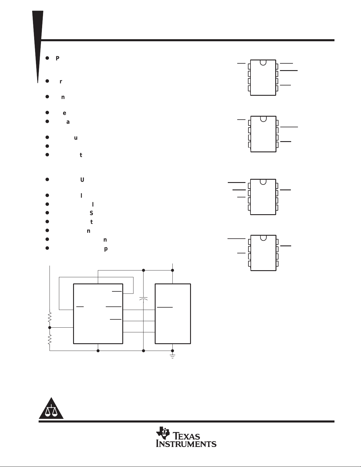
TPS3705 ...D PACKAGE
(TOP VIEW)
MR
1
V
GND
V
GND
NC – No internal connection
TPS3705 . . . DGN PACKAGE
RESET
WDO
V
TPS3707 . . . DGN PACKAGE
RESET
RESET
5 V12 V
V
2
DD
3
4
PFI
TPS3707 ...D PACKAGE
(TOP VIEW)
MR
1
2
DD
3
4
PFI
(TOP VIEW)
1
2
MR
3
4
DD
(TOP VIEW)
1
2
MR
3
4
DD
8
7
6
5
8
7
6
5
8
7
6
5
8
7
6
5
WDO
RESET
WDI
PFO
RESET
RESET
NC
PFO
WDI
PFO
PFI
GND
NC
PFO
PFI
GND
V
DD
PFO
910 kΩ
120 kΩ
TPS3705–50
MR RESET
PFI
GND
100 nF
WDO
WDI
Figure 1. Typical MSP430 Application
Please be aware that an important notice concerning availability, standard warranty, and use in critical applications of
Texas Instruments semiconductor products and disclaimers thereto appears at the end of this data sheet.
PRODUCTION DATA information is current as of publication date.
Products conform to specifications per the terms of Texas Instruments
standard warranty. Production processing does not necessarily include
testing of all parameters.
V
DD
MSP430P112
RESET/NMI
I/O
I/O
GND
NC – No internal connection
Copyright 1999, Texas Instruments Incorporated
POST OFFICE BOX 655303 • DALLAS, TEXAS 75265
1
Page 2
TPS3705-30, TPS3705-33, TPS3705-50
TPS3707-25, TPS3707-30, TPS3707-33, TPS3707-50
PROCESSOR SUPERVISORY CIRCUITS WITH POWER-FAIL
SLVS184B – NOVEMBER 1998 – REVISED JANUAR Y 1999
description
The TPS3705, TPS3707 family of microprocessor supply-voltage supervisors provide circuit initialization and
timing supervision, primarily for DSP and processor-based systems.
During power-on, RESET
supply voltage supervisor monitors V
voltage V
. An internal timer delays the return of the output to the inactive state (high) to ensure proper system
IT+
reset. The delay time, t
voltage drops below the threshold voltage V
is asserted when the supply voltage V
and keeps RESET active as long as VDD remains below the threshold
DD
= 200 ms, starts after V
d typ
IT–
has risen above the threshold voltage V
DD
, the output becomes active (low) again. No external components
are required. All the devices of this family have a fixed-sense threshold voltage V
becomes higher than 1.1 V . Thereafter , the
DD
. When the supply
IT+
set by an internal voltage
IT–
divider.
The TPS3705-xx and TPS3707-xx devices incorporate a manual reset input, MR
RESET
to become active.
. A low level at MR causes
The TPS370x-xx families integrate a power-fail comparator which can be used for low-battery detection,
power-fail warning, or for monitoring a power supply other than the main supply.
The TPS3705-xx devices have a watchdog timer that is periodically triggered by a positive or negative transition
at WDI. When the supervising system fails to retrigger the watchdog circuit within the time-out interval,
t
= 1.6 s, WDO becomes active. This event also reinitializes the watchdog timer. Leaving WDI unconnected
t(out)
disables the watchdog.
The TPS3707-xx devices do not have the Watchdog function, but include a high-level output RESET.
The product spectrum is designed for supply voltages of 2.5 V , 3 V, 3.3 V, and 5 V . The circuits are available in
either 8-pin MSOP or standard SOIC packages. The TPS3705, TPS3707 devices are characterized for
operation over a temperature range of –40°C to 85°C.
AVAILABLE OPTIONS
PACKAGED DEVICES
T
A
–40°C to 85°C
THRESHOLD
VOLTAGE
2.63 V TPS3705–30D TPS3705–30DGN TIAAT TPS3705-30Y
2.93 V TPS3705–33D TPS3705–33DGN TIAAU TPS3705–33Y
4.55 V TPS3705–50D TPS3705–50DGN TIAAV TPS3705–50Y
2.25 V TPS3707–25D TPS3707–25DGN TIAAW TPS3707–25Y
2.63 V TPS3707–30D TPS3707–30DGN TIAAX TPS3707–30Y
2.93 V TPS3707–33D TPS3707–33DGN TIAAY TPS3707–33Y
4.55 V TPS3707–50D TPS3707–50DGN TIAAZ TPS3707–50Y
SMALL OUTLINE
(D)
POWER–PAD
µ-SMALL OUTLINE
(DGN)
MARKING DGN
PACKAGE
CHIP FORM
(Y)
2
POST OFFICE BOX 655303 • DALLAS, TEXAS 75265
Page 3
TPS3705-30, TPS3705-33, TPS3705-50
TPS3707-25, TPS3707-30, TPS3707-33, TPS3707-50
PROCESSOR SUPERVISORY CIRCUITS WITH POWER-FAIL
SLVS184B – NOVEMBER 1998 – REVISED JANUAR Y 1999
Function Tables
TRUTH TABLE, TPS3705
VDD>V
MR
H→L 1 H→L 30 ns
L→H 1L→H200 ms
H 1→0H→L 3 µs
H 0→1 L→H 200 ms
TRUTH TABLE, TPS3707
MR
H→L 1 H→L L→H 30 ns
L→H 1L→HH→L 200 ms
VDD>V
IT
H 1→0H→LL→H3 µs
H0→1L→HH→L200 ms
TRUTH TABLE, TPS370x
PFI>V
IT
0→1 L→H 0.5 µs
1→0 H→L 0.5 µs
IT
RESET
PFO
RESET
TYPICAL
DELAY
RESET
TYPICAL
DELAY
TYPICAL
DELAY
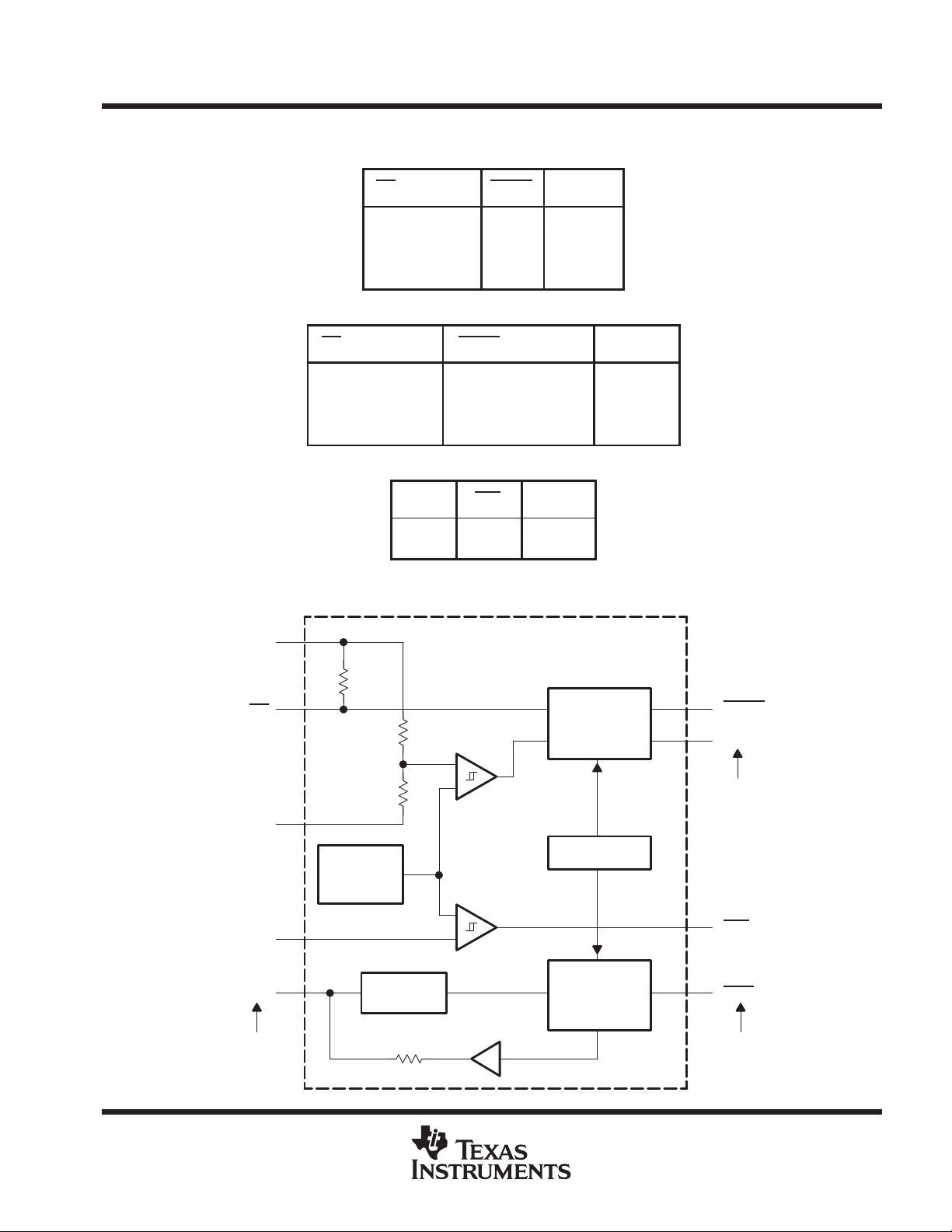
functional block diagram
V
DD
MR
GND
PFI
WDI
14 kΩ
R1
R2
Reference
Voltage
of 1.25 V
Transition
Detection
+
_
_
+
TPS3705
TPS3707
Reset
Logic + Timer
Oscillator
Watchdog
Logic + Timer
RESET
RESET
Only
TPS3707
PFO
WDO
Only
TPS3705
40 kΩ
POST OFFICE BOX 655303 • DALLAS, TEXAS 75265
Only
TPS3705
3
Page 4
TPS3705-30, TPS3705-33, TPS3705-50
TPS3707-25, TPS3707-30, TPS3707-33, TPS3707-50
PROCESSOR SUPERVISORY CIRCUITS WITH POWER-FAIL
SLVS184B – NOVEMBER 1998 – REVISED JANUAR Y 1999
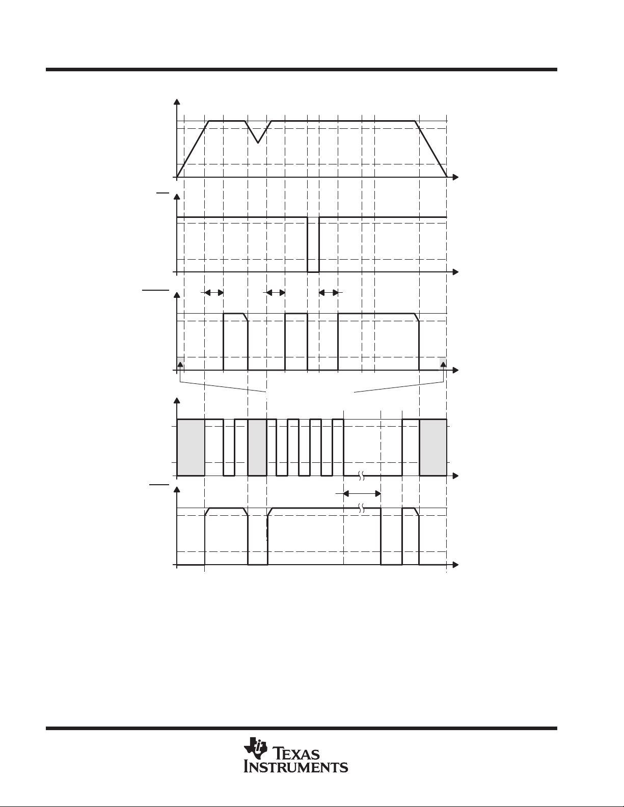
timing diagrams
V
DD
5 V
4.5 V
1.1 V
0 V
MR
5 V
4.5 V
1.1 V
0 V
t
t
RESET
5 V
4.5 V
1.1 V
0 V
WDI
5 V
4.5 V
1.1 V
0 V
WDO
5 V
4.5 V
1.1 V
0 V
t
d
Don’t Care
t
d
Undefined Behavior
Don’t Care
t
t(out)
t
d
t
Don’t Care
t
t
4
POST OFFICE BOX 655303 • DALLAS, TEXAS 75265
Page 5
I/O
DESCRIPTION
6
8
TPS3705-30, TPS3705-33, TPS3705-50
TPS3707-25, TPS3707-30, TPS3707-33, TPS3707-50
PROCESSOR SUPERVISORY CIRCUITS WITH POWER-FAIL
SLVS184B – NOVEMBER 1998 – REVISED JANUAR Y 1999
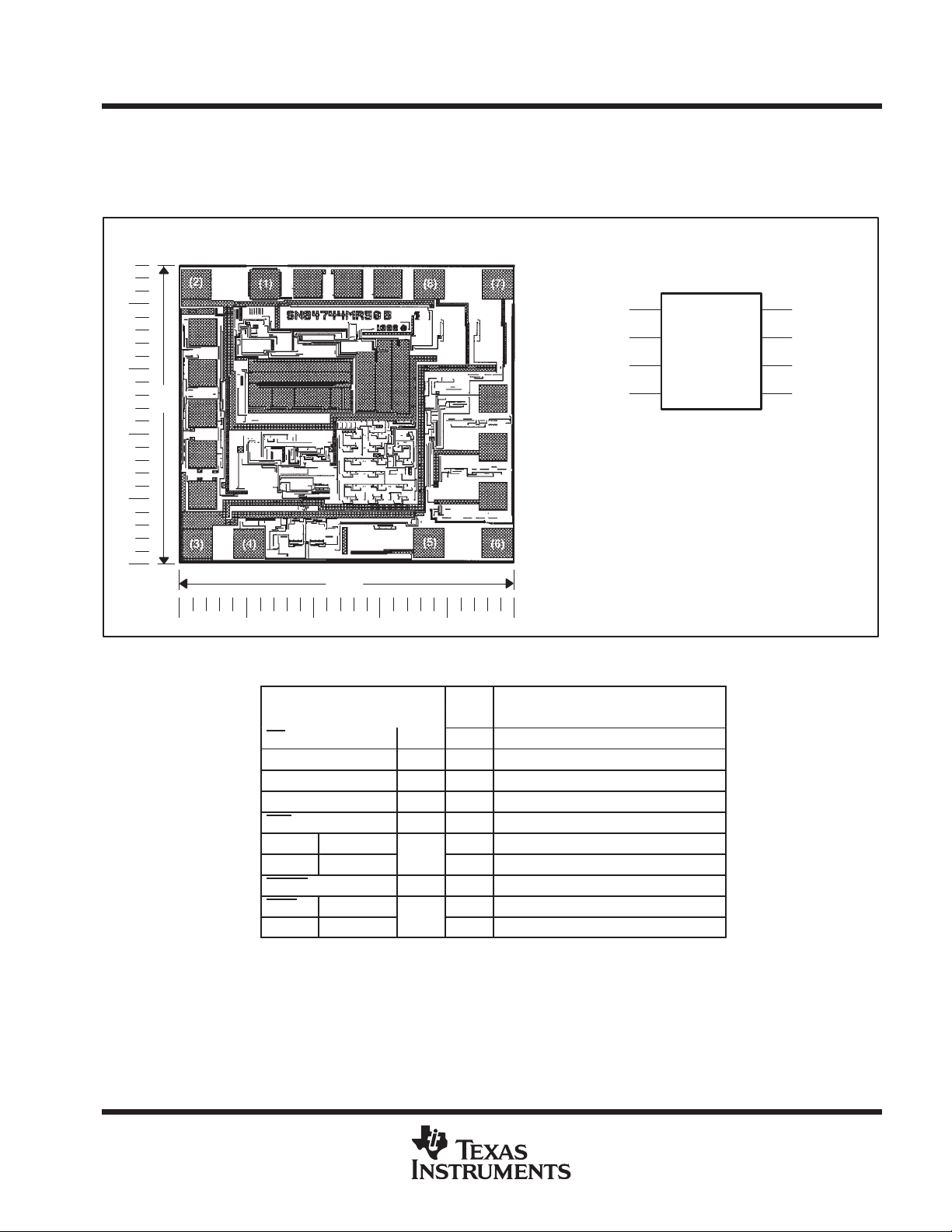
TPS370xY chip information
These chips, when properly assembled, display characteristics similar to those of the TPS370x. Thermal
compression or ultrasonic bonding may be caused on the doped-aluminum bonding pads. The chips may be
mounted with conductive epoxy or a gold-silicon preform.
BONDING PAD ASSIGNMENTS
46
(1)
(2)
(3)
(4)
CHIP THICKNESS: 10 MILS TYPICAL
BONDING PADS: 4 × 4 MINIMUM
TJ max = 150°C
TOLERANCES ARE ±10%
ALL DIMENSIONS ARE IN MILS
50
Terminal Functions
TERMINAL
NAME NO.
MR 1 I Manual reset
VDD 2 Supply voltage
GND 3 Ground
PFI 4 I Power-fail comparator input
PFO 5 O Power-fail comparator output
WDI TPS3705
NC TPS3707
RESET 7 O Active-low reset output
WDO TPS3705
RESET TPS3707
I Watchdog timer input
No internal connection
O Watchdog timer output
O Active-high reset output
TPS3705Y
TPS3707Y
(8)
(7)
(6)
(5)
POST OFFICE BOX 655303 • DALLAS, TEXAS 75265
5
Page 6

TPS3705-30, TPS3705-33, TPS3705-50
TPS3707-25, TPS3707-30, TPS3707-33, TPS3707-50
PROCESSOR SUPERVISORY CIRCUITS WITH POWER-FAIL
SLVS184B – NOVEMBER 1998 – REVISED JANUAR Y 1999
absolute maximum ratings over operating free-air temperature (unless otherwise noted)
Supply voltage, V
(see Note1) 7 V. . . . . . . . . . . . . . . . . . . . . . . . . . . . . . . . . . . . . . . . . . . . . . . . . . . . . . . . . . . . . .
DD
†
All other pins (see Note 1) –0.3 V to 7 V. . . . . . . . . . . . . . . . . . . . . . . . . . . . . . . . . . . . . . . . . . . . . . . . . . . . . . . . . . .
Maximum low output current, I
Maximum high output current, I
Input clamp current, I
Output clamp current, I
IK
(V
OK
< 0 or V
I
(V
O
OL
OH
> VDD) ±20 mA. . . . . . . . . . . . . . . . . . . . . . . . . . . . . . . . . . . . . . . . . . . . . . . . .
I
< 0 or V
> VDD) ±20 mA. . . . . . . . . . . . . . . . . . . . . . . . . . . . . . . . . . . . . . . . . . . .
O
5 mA. . . . . . . . . . . . . . . . . . . . . . . . . . . . . . . . . . . . . . . . . . . . . . . . . . . . . . . . . . . .
–5 mA. . . . . . . . . . . . . . . . . . . . . . . . . . . . . . . . . . . . . . . . . . . . . . . . . . . . . . . . . .
Continuous total power dissipation See Dissipation Rating Table. . . . . . . . . . . . . . . . . . . . . . . . . . . . . . . . . . . . . .
Operating free-air temperature range, T
Storage temperature range, T
stg
A
–40°C to 85°C. . . . . . . . . . . . . . . . . . . . . . . . . . . . . . . . . . . . . . . . . . . . .
–65°C to 150°C. . . . . . . . . . . . . . . . . . . . . . . . . . . . . . . . . . . . . . . . . . . . . . . . . . . .
Soldering temperature 260°C. . . . . . . . . . . . . . . . . . . . . . . . . . . . . . . . . . . . . . . . . . . . . . . . . . . . . . . . . . . . . . . . . . . .
†
Stresses beyond those listed under “absolute maximum ratings” may cause permanent damage to the device. These are stress ratings only, and
functional operation of the device at these or any other conditions beyond those indicated under “recommended operating conditions” is not
implied. Exposure to absolute–maximum–rated conditions for extended periods may affect device reliability.
NOTE 1: All voltage values are with respect to GND. For reliable operation the device must not be operated at 7 V for more than t = 1000h
continuously.
PACKAGE
DGN
D
TA <25°C
POWER RATING
2.14 W
725 mW
DISSIPATION RATING TABLE
DERATING FACTOR
ABOVE TA = 25°C
17.1 mW/_C
5.8 mW/_C
TA = 70°C
POWER RATING
1.37 W
464 mW
TA = 85°C
POWER RATING
1.11 W
377 mW
recommended operating conditions at specified temperature range
MIN MAX UNIT
Supply voltage, V
Input voltage, V
High-level input voltage, V
Low-level input voltage, V
Input transition rise and fall rate at MR or WDI, ∆t/∆V 100 ns/V
Operating free-air temperature range, T
DD
I
IH
IL
A
2 6 V
0 VDD+0.3 V
0.7×V
DD
0.3×V
DD
–40 85
V
V
_
C
6
POST OFFICE BOX 655303 • DALLAS, TEXAS 75265
Page 7

V
V
I
OH
500 µA
DD
VOLLow-level out ut voltage
0.4
T
0°C to 85°C
V
Negative going in ut
T
40°C to 85°C
V
V
y
WDI
IIHHigh-level input current
A
IILLow-level input current
A
IDDSupply current
TPS3705-30, TPS3705-33, TPS3705-50
TPS3707-25, TPS3707-30, TPS3707-33, TPS3707-50
PROCESSOR SUPERVISORY CIRCUITS WITH POWER-FAIL
SLVS184B – NOVEMBER 1998 – REVISED JANUAR Y 1999
electrical characteristics over recommended operating free-air temperature range (unless
otherwise noted)
PARAMETER TEST CONDITIONS MIN TYP MAX UNIT
TPS370x-xx VDD = 1.1 V IOH = –4 µA 0.8
TPS3707-25
TPS370x-30
V
OH
V
IT–
V
hys
I
IH(AV)
I
IL(AV)
I
I
C
i
NOTES: 2. The lowest supply voltage at which RESET becomes active. t
High-level output voltage
-
Power-up reset voltage (see Note 2) VDD ≥ 1.1 V, IOL = 50 µA 0.3 V
Negative-going input
threshold voltage
(see Note 3)
Hysteresis
Average high-level input
current
Average low-level input
current
Input current PFI VDD = 6 V, 0 V ≤ VI ≤ V
pp
Input capacitance VI = 0 V to V
3. T o ensure best stability of the threshold voltage, a bypass capacitor (ceramic, 0.1 µF) should be placed near to the supply terminals.
p
p
p
TPS370x-33
TPS370x-50
TPS370x-xx VDD = 6 V, IOH = –800 µA
TPS3707-25
TPS370x-30
TPS370x-33
TPS370x-50
TPS370x-xx VDD = 6 V IOL = 3 mA
TPS3707-25 2.20 2.25 2.30
TPS370x-30
TPS370x-33
TPS370x-50 4.45 4.55 4.63
TPS3707-25 2.20 2.25 2.32
TPS370x-30
TPS370x-33
TPS370x-50 4.45 4.55 4.65
PFI TPS370x-xx VDD ≥ 2 V, TA = –40°C to 85°C 1.20 1.25 1.30 V
TPS3707-25 40
TPS370x-30 50
DD
TPS370x-33 50
TPS370x-50 70
PFI TPS370x-xx 10
WDI WDI = VDD = 6 V 120 170
MR MR = 0.7×V
WDI WDI = 0 V, VDD = 6 V –120 –170
MR MR = 0 V, VDD = 6 V –430 –600
TPS3707-xx
TPS3705-xx
=
DD
VDD = V
IOH = –800 µA
VDD = V
VDD = V
IOL = 2.5 mA
=
A
= –
A
WDI = VDD = 6 V,
Time average (dc = 88%)
WDI = 0 V, VDD = 6 V,
Time average (dc = 12%)
VDD = 2 V to 6 V, MR = VDD, MR,
WDI and outputs unconnected
VDD = 2 V to 6 V, MR= V
WDI and outputs unconnected
+ 0.2 V,
IT+
=
=–
+ 0.2 V,
IT+
+0.2 V, IOL = 1 mA 0.3 V
IT+
+0.2 V ,
IT+
°
°
°
°
DD,VDD
r,VDD
= 6 V –130 –180
DD
MR,
DD,
DD
≥ 15 µs/V
0.7×V
DD
VDD –1.5 V
2.57 2.63 2.68
2.87 2.93 2.98
2.57 2.63 2.70
2.87 2.93 3.0
100 150 µA
–15 –20 µA
–1 0 1 µA
20 50 µA
30 50 µA
5 pF
V
V
mV
µ
µ
POST OFFICE BOX 655303 • DALLAS, TEXAS 75265
7
Page 8

TPS3705-30, TPS3705-33, TPS3705-50
V
IL
× V
DD
ns
s
PFI to PFO del
V
2 V to 6 V
s
TPS3707-25, TPS3707-30, TPS3707-33, TPS3707-50
PROCESSOR SUPERVISORY CIRCUITS WITH POWER-FAIL
SLVS184B – NOVEMBER 1998 – REVISED JANUAR Y 1999
timing requirements at R
PARAMETER TEST CONDITIONS MIN TYP MAX UNIT
at V
DDVDD
t
w
Pulse width
at MR VDD ≥ V
at WDI VDD ≥ V
switching characteristics at R
t
Watchdog time out
t(out)
t
Delay time
d
Propagation (delay) time, high-to-low-level
t
PHL
output
Propagation (delay) time, low-to-high-level
t
PLH
output
Propagation (delay) time, high-to-low-level
t
PHL
output
Propagation (delay) time, low-to-high-level
t
PLH
output
Propagation (delay) time, high-to-low-level
t
PHL
output
Propagation (delay) time, low-to-high-level
t
PLH
output
= 1 MΩ, C
L
= V
+ 0.2 V, VDD = V
IT+
+ 0.2 V, VIL = 0.3 × VDD, VIH = 0.7 × V
IT+
+ 0.2 V, VIL = 0.3 × VDD, VIH = 0.7 × V
IT+
= 1 MΩ, C
L
PARAMETER TEST CONDITIONS MIN TYP MAX UNIT
= 50 pF, T
L
IT–
= 50 pF, T
L
MR to RESET delay
MR to RESET delay
(TPS3707–xx only)
VDD to RESET delay
VDD to RESET delay
(TPS3707-xx only)
= 25°C
A
–0.2 V 6 µs
100 ns
100 ns
1.1 1.6 2.3 s
140 200 280 ms
50 250
50 250
0.5 1
0.5 1
ay
= 25°C
A
VDD ≥ V
See timing diagram
VDD > V
See timing diagram
VDD ≥ V
= 0.3
VIH = 0.7 × V
DD
=
DD
DD
IT+
IT+
IT+
+ 0.2 V,
+ 0.2 V,
+ 0.2 V,
DD
3 5
µ
3 5
µ
8
POST OFFICE BOX 655303 • DALLAS, TEXAS 75265
Page 9

TPS3705-30, TPS3705-33, TPS3705-50
TPS3707-25, TPS3707-30, TPS3707-33, TPS3707-50
PROCESSOR SUPERVISORY CIRCUITS WITH POWER-FAIL
SLVS184B – NOVEMBER 1998 – REVISED JANUAR Y 1999
TYPICAL CHARACTERISTICS
NORMALIZED INPUT THRESHOLD VOLTAGE
vs
C
°
FREE-AIR TEMPERATURE AT V
1.002
1.001
1
DD
VDD = 6 V
PFI = 1.05 V
MR
= Open
SUPPLY CURRENT
SUPPLY VOLTAGE
50
PFI = 1.05 V
MR
= Open
TA = 25°C
30
AµI
10
–10
– Supply Current –
DD
–30
–50
–0.5 0.5 2.5 3.5
VDD – Supply Voltage – V
0.999
Normalized Input Threshold Voltage VIT(TA), VIT (25 )
vs
TPS3707–50
Figure 3
–40 –15 10 35
TA – Free-Air Temperature – °C
Figure 2
4.5 6.51.5 5.5
60 85
INPUT CURRENT
INPUT VOLTAGE AT MR
100
VDD = 6 V
PFI = 1.05 V
0
A
µ
–100
–200
– Input Current –
–300
I
I
–40°C
–400
85°C
–500
–10123
V
– Input Voltage at MR
I
Figure 4
vs
456
– V
POST OFFICE BOX 655303 • DALLAS, TEXAS 75265
9
Page 10

TPS3705-30, TPS3705-33, TPS3705-50
TPS3707-25, TPS3707-30, TPS3707-33, TPS3707-50
PROCESSOR SUPERVISORY CIRCUITS WITH POWER-FAIL
SLVS184B – NOVEMBER 1998 – REVISED JANUAR Y 1999
TYPICAL CHARACTERISTICS
MINIMUM PULSE DURATION AT V
THRESHOLD OVERDRIVE
V
DD
10
sµ
–
8
DD
V
6
4
2
– Minimum Pulse Duration at
w
t
0
0 200 400 600
VDD – Threshold Overdrive – mV
Figure 5
HIGH-LEVEL OUTPUT VOLTAGE
HIGH-LEVEL OUTPUT CURRENT
6.5
6
5.5
5
4.5
4
3.5
3
2.5
2
– High-Level Output Voltage – V
1.5
OH
1
V
0.5
0
0 –5 –10 –15
IOH – High-Level Output Current – mA
Figure 7
vs
85°C
PFI = 1.05 V
MR
vs
VDD = 6 V
PFI = 1.05 V
MR
–20 –25 –30
DD
= Open
800 1000
= Open
–40°C
HIGH-LEVEL OUTPUT VOLTAGE
HIGH-LEVEL OUTPUT CURRENT
3.5
3
2.5
2
1.5
1
– High-Level Output Voltage – V
OH
V
0.5
0
0–1–2–3–4–5–6
IOH – High-Level Output Current – mA
LOW-LEVEL OUTPUT VOLTAGE
LOW-LEVEL OUTPUT CURRENT
3
VDD = 2.67 V
PFI = 1.05 V
MR
2.5
1.5
– Low-Level Output Voltage – V
OL
0.5
V
= Open
2
1
0
01234 67
IOL – Low-Level Output Current – mA
85°C
Figure 6
85°C
Figure 8
vs
VDD = 3.2 V
PFI = 1.05 V
MR
= Open
–40°C
–7 –8 –9 –10
vs
–40°C
89 11 1351012
10
POST OFFICE BOX 655303 • DALLAS, TEXAS 75265
Page 11

TPS3705-30, TPS3705-33, TPS3705-50
TPS3707-25, TPS3707-30, TPS3707-33, TPS3707-50
PROCESSOR SUPERVISORY CIRCUITS WITH POWER-FAIL
SLVS184B – NOVEMBER 1998 – REVISED JANUAR Y 1999
MECHANICAL DATA
D (R-PDSO-G**) PLASTIC SMALL-OUTLINE PACKAGE
14 PIN SHOWN
0.050 (1,27)
14
1
0.069 (1,75) MAX
A
0.020 (0,51)
0.014 (0,35)
0.010 (0,25)
0.004 (0,10)
DIM
8
7
PINS **
0.010 (0,25)
0.157 (4,00)
0.150 (3,81)
M
0.244 (6,20)
0.228 (5,80)
Seating Plane
0.004 (0,10)
8
14
0.008 (0,20) NOM
0°–8°
16
Gage Plane
0.010 (0,25)
0.044 (1,12)
0.016 (0,40)
A MAX
A MIN
NOTES: A. All linear dimensions are in inches (millimeters).
B. This drawing is subject to change without notice.
C. Body dimensions do not include mold flash or protrusion, not to exceed 0.006 (0,15).
D. Falls within JEDEC MS-012
POST OFFICE BOX 655303 • DALLAS, TEXAS 75265
0.197
(5,00)
0.189
(4,80)
0.344
(8,75)
0.337
(8,55)
0.394
(10,00)
0.386
(9,80)
4040047/D 10/96
11
Page 12

TPS3705-30, TPS3705-33, TPS3705-50
TPS3707-25, TPS3707-30, TPS3707-33, TPS3707-50
PROCESSOR SUPERVISORY CIRCUITS WITH POWER-FAIL
SLVS184B – NOVEMBER 1998 – REVISED JANUAR Y 1999
MECHANICAL DATA
DGN (S-PDSO-G8) PowerPAD PLASTIC SMALL-OUTLINE PACKAGE
0,65
8
1
1,07 MAX
3,05
2,95
0,38
0,25
5
3,05
2,95
4
Seating Plane
0,15
0,05
0,25
4,98
4,78
M
0,10
Thermal Pad
(See Note D)
0,15 NOM
0°–6°
Gage Plane
0,25
0,69
0,41
NOTES: A. All linear dimensions are in millimeters.
B. This drawing is subject to change without notice.
C. Body dimensions include mold flash or protrusions.
D. The package thermal performance may be enhanced by attaching an external heat sink to the thermal pad. This pad is electrically
and thermally connected to the backside of the die and possibly selected leads.
E. Falls within JEDEC MO-187
PowerPAD is a trademark of Texas Instruments Incorporated.
4073271/A 01/98
12
POST OFFICE BOX 655303 • DALLAS, TEXAS 75265
Page 13

PACKAGE OPTION ADDENDUM
www.ti.com
13-Sep-2005
PACKAGING INFORMATION
Orderable Device Status
TPS3705-30D ACTIVE SOIC D 8 75 Green (RoHS &
TPS3705-30DGN ACTIVE MSOP-
TPS3705-30DR ACTIVE SOIC D 8 2500 Green (RoHS &
TPS3705-30DRG4 ACTIVE SOIC D 8 2500 Green (RoHS &
TPS3705-33D ACTIVE SOIC D 8 75 Green (RoHS &
TPS3705-33DGN ACTIVE MSOP-
TPS3705-33DGNG4 ACTIVE MSOP-
TPS3705-33DGNR ACTIVE MSOP-
TPS3705-33DGNRG4 ACTIVE MSOP-
TPS3705-33DR ACTIVE SOIC D 8 2500 Green (RoHS &
TPS3705-33DRG4 ACTIVE SOIC D 8 2500 Green (RoHS &
TPS3705-50D ACTIVE SOIC D 8 75 Green (RoHS &
TPS3705-50DGN ACTIVE MSOP-
TPS3705-50DGNG4 ACTIVE MSOP-
TPS3705-50DGNR ACTIVE MSOP-
TPS3705-50DGNRG4 ACTIVE MSOP-
TPS3705-50DR ACTIVE SOIC D 8 2500 Green (RoHS &
TPS3705-50DRG4 ACTIVE SOIC D 8 2500 Green (RoHS &
TPS3707-25D ACTIVE SOIC D 8 75 Green (RoHS &
TPS3707-25DGN ACTIVE MSOP-
TPS3707-25DGNG4 ACTIVE MSOP- DGN 8 80 Green(RoHS & CU NIPDAU Level-1-260C-UNLIM
(1)
Package
Type
Power
PAD
Power
PAD
Power
PAD
Power
PAD
Power
PAD
Power
PAD
Power
PAD
Power
PAD
Power
PAD
Power
PAD
Package
Drawing
DGN 8 80 Green (RoHS &
DGN 8 80 Green (RoHS &
DGN 8 80 Green (RoHS &
DGN 8 2500 Green (RoHS &
DGN 8 2500 Green (RoHS &
DGN 8 80 Green (RoHS &
DGN 8 80 Green (RoHS &
DGN 8 2500 Green (RoHS &
DGN 8 2500 Green (RoHS &
DGN 8 80 Green (RoHS &
Pins Package
Qty
Eco Plan
no Sb/Br)
no Sb/Br)
no Sb/Br)
no Sb/Br)
no Sb/Br)
no Sb/Br)
no Sb/Br)
no Sb/Br)
no Sb/Br)
no Sb/Br)
no Sb/Br)
no Sb/Br)
no Sb/Br)
no Sb/Br)
no Sb/Br)
no Sb/Br)
no Sb/Br)
no Sb/Br)
no Sb/Br)
no Sb/Br)
(2)
Lead/Ball Finish MSL Peak Temp
CU NIPDAU Level-1-260C-UNLIM
CU NIPDAU Level-1-260C-UNLIM
CU NIPDAU Level-1-260C-UNLIM
CU NIPDAU Level-1-260C-UNLIM
CU NIPDAU Level-1-260C-UNLIM
CU NIPDAU Level-1-260C-UNLIM
CU NIPDAU Level-1-260C-UNLIM
CU NIPDAU Level-1-260C-UNLIM
CU NIPDAU Level-1-260C-UNLIM
CU NIPDAU Level-1-260C-UNLIM
CU NIPDAU Level-1-260C-UNLIM
CU NIPDAU Level-1-260C-UNLIM
CU NIPDAU Level-1-260C-UNLIM
CU NIPDAU Level-1-260C-UNLIM
CU NIPDAU Level-1-260C-UNLIM
CU NIPDAU Level-1-260C-UNLIM
CU NIPDAU Level-1-260C-UNLIM
CU NIPDAU Level-1-260C-UNLIM
CU NIPDAU Level-1-260C-UNLIM
CU NIPDAU Level-1-260C-UNLIM
(3)
Addendum-Page 1
Page 14

PACKAGE OPTION ADDENDUM
www.ti.com
Orderable Device Status
(1)
Package
Type
Power
Package
Drawing
Pins Package
Qty
Eco Plan
no Sb/Br)
(2)
Lead/Ball Finish MSL Peak Temp
13-Sep-2005
PAD
TPS3707-25DGNR ACTIVE MSOP-
Power
DGN 8 2500 Green (RoHS &
no Sb/Br)
CU NIPDAU Level-1-260C-UNLIM
PAD
TPS3707-25DGNRG4 ACTIVE MSOP-
Power
DGN 8 2500 Green (RoHS &
no Sb/Br)
CU NIPDAU Level-1-260C-UNLIM
PAD
TPS3707-25DR ACTIVE SOIC D 8 2500 Green (RoHS &
CU NIPDAU Level-1-260C-UNLIM
no Sb/Br)
TPS3707-25DRG4 ACTIVE SOIC D 8 2500 Green (RoHS &
CU NIPDAU Level-1-260C-UNLIM
no Sb/Br)
TPS3707-30D ACTIVE SOIC D 8 75 Green (RoHS &
CU NIPDAU Level-1-260C-UNLIM
no Sb/Br)
TPS3707-30DGN ACTIVE MSOP-
Power
DGN 8 80 Green (RoHS &
no Sb/Br)
CU NIPDAU Level-1-260C-UNLIM
PAD
TPS3707-30DGNG4 ACTIVE MSOP-
Power
DGN 8 80 Green (RoHS &
no Sb/Br)
CU NIPDAU Level-1-260C-UNLIM
PAD
TPS3707-30DGNR ACTIVE MSOP-
Power
DGN 8 2500 Green (RoHS &
no Sb/Br)
CU NIPDAU Level-1-260C-UNLIM
PAD
TPS3707-30DGNRG4 ACTIVE MSOP-
Power
DGN 8 2500 Green (RoHS &
no Sb/Br)
CU NIPDAU Level-1-260C-UNLIM
PAD
TPS3707-30DR ACTIVE SOIC D 8 2500 Green (RoHS &
CU NIPDAU Level-1-260C-UNLIM
no Sb/Br)
TPS3707-30DRG4 ACTIVE SOIC D 8 2500 Green (RoHS &
CU NIPDAU Level-1-260C-UNLIM
no Sb/Br)
TPS3707-33D ACTIVE SOIC D 8 75 Green (RoHS &
CU NIPDAU Level-1-260C-UNLIM
no Sb/Br)
TPS3707-33DG4 ACTIVE SOIC D 8 75 Green (RoHS &
CU NIPDAU Level-1-260C-UNLIM
no Sb/Br)
TPS3707-33DGN ACTIVE MSOP-
Power
DGN 8 80 Green (RoHS &
no Sb/Br)
CU NIPDAU Level-1-260C-UNLIM
PAD
TPS3707-33DGNG4 ACTIVE MSOP-
Power
DGN 8 80 Green (RoHS &
no Sb/Br)
CU NIPDAU Level-1-260C-UNLIM
PAD
TPS3707-33DGNR ACTIVE MSOP-
Power
DGN 8 2500 Green (RoHS &
no Sb/Br)
CU NIPDAU Level-1-260C-UNLIM
PAD
TPS3707-33DGNRG4 ACTIVE MSOP-
Power
DGN 8 2500 Green (RoHS &
no Sb/Br)
CU NIPDAU Level-1-260C-UNLIM
PAD
TPS3707-33DR ACTIVE SOIC D 8 2500 Green (RoHS &
CU NIPDAU Level-1-260C-UNLIM
no Sb/Br)
TPS3707-33DRG4 ACTIVE SOIC D 8 2500 Green (RoHS &
CU NIPDAU Level-1-260C-UNLIM
no Sb/Br)
TPS3707-50D ACTIVE SOIC D 8 75 Green (RoHS &
CU NIPDAU Level-1-260C-UNLIM
no Sb/Br)
TPS3707-50DGN ACTIVE MSOP- DGN 8 80 Green (RoHS & CU NIPDAU Level-1-260C-UNLIM
(3)
Addendum-Page 2
Page 15

PACKAGE OPTION ADDENDUM
www.ti.com
Orderable Device Status
(1)
Package
Type
Power
Package
Drawing
Pins Package
Qty
Eco Plan
no Sb/Br)
(2)
Lead/Ball Finish MSL Peak Temp
13-Sep-2005
(3)
PAD
TPS3707-50DGNR ACTIVE MSOP-
Power
DGN 8 2500 Green (RoHS &
no Sb/Br)
CU NIPDAU Level-1-260C-UNLIM
PAD
TPS3707-50DGNRG4 ACTIVE MSOP-
Power
DGN 8 2500 Green (RoHS &
no Sb/Br)
CU NIPDAU Level-1-260C-UNLIM
PAD
TPS3707-50DR ACTIVE SOIC D 8 2500 Green (RoHS &
CU NIPDAU Level-1-260C-UNLIM
no Sb/Br)
TPS3707-50DRG4 ACTIVE SOIC D 8 2500 Green (RoHS &
CU NIPDAU Level-1-260C-UNLIM
no Sb/Br)
(1)
The marketing status values are defined as follows:
ACTIVE: Product device recommended for new designs.
LIFEBUY: TI has announced that the device will be discontinued, and a lifetime-buy period is in effect.
NRND: Not recommended for new designs. Device is in production to support existing customers, but TI does not recommend using this part in
a new design.
PREVIEW: Device has been announced but is not in production. Samples may or may not be available.
OBSOLETE: TI has discontinued the production of the device.
(2)
Eco Plan - The planned eco-friendly classification: Pb-Free (RoHS) or Green (RoHS & no Sb/Br) - please check
http://www.ti.com/productcontent for the latest availability information and additional product content details.
TBD: The Pb-Free/Green conversion plan has not been defined.
Pb-Free (RoHS): TI's terms "Lead-Free" or "Pb-Free" mean semiconductor products that are compatible with the current RoHS requirements
for all 6 substances, including the requirement that lead not exceed 0.1% by weight in homogeneous materials. Where designed to be soldered
at high temperatures, TI Pb-Free products are suitable for use in specified lead-free processes.
Green (RoHS & no Sb/Br): TI defines "Green" to mean Pb-Free (RoHS compatible), and free of Bromine (Br) and Antimony (Sb) based flame
retardants (Br or Sb do not exceed 0.1% by weight in homogeneous material)
(3)
MSL, Peak Temp. -- The Moisture Sensitivity Level rating according to the JEDEC industry standard classifications, and peak solder
temperature.
Important Information and Disclaimer:The information provided on this page represents TI's knowledge and belief as of the date that it is
provided. TI bases its knowledge and belief on information provided by third parties, and makes no representation or warranty as to the
accuracy of such information. Efforts are underway to better integrate information from third parties. TI has taken and continues to take
reasonable steps to provide representative and accurate information but may not have conducted destructive testing or chemical analysis on
incoming materials and chemicals. TI and TI suppliers consider certain information to be proprietary, and thus CAS numbers and other limited
information may not be available for release.
In no event shall TI's liability arising out of such information exceed the total purchase price of the TI part(s) at issue in this document sold by TI
to Customer on an annual basis.
Addendum-Page 3
Page 16

IMPORTANT NOTICE
Texas Instruments Incorporated and its subsidiaries (TI) reserve the right to make corrections, modifications,
enhancements, improvements, and other changes to its products and services at any time and to discontinue
any product or service without notice. Customers should obtain the latest relevant information before placing
orders and should verify that such information is current and complete. All products are sold subject to TI’s terms
and conditions of sale supplied at the time of order acknowledgment.
TI warrants performance of its hardware products to the specifications applicable at the time of sale in
accordance with TI’s standard warranty. Testing and other quality control techniques are used to the extent TI
deems necessary to support this warranty . Except where mandated by government requirements, testing of all
parameters of each product is not necessarily performed.
TI assumes no liability for applications assistance or customer product design. Customers are responsible for
their products and applications using TI components. To minimize the risks associated with customer products
and applications, customers should provide adequate design and operating safeguards.
TI does not warrant or represent that any license, either express or implied, is granted under any TI patent right,
copyright, mask work right, or other TI intellectual property right relating to any combination, machine, or process
in which TI products or services are used. Information published by TI regarding third-party products or services
does not constitute a license from TI to use such products or services or a warranty or endorsement thereof.
Use of such information may require a license from a third party under the patents or other intellectual property
of the third party, or a license from TI under the patents or other intellectual property of TI.
Reproduction of information in TI data books or data sheets is permissible only if reproduction is without
alteration and is accompanied by all associated warranties, conditions, limitations, and notices. Reproduction
of this information with alteration is an unfair and deceptive business practice. TI is not responsible or liable for
such altered documentation.
Resale of TI products or services with statements different from or beyond the parameters stated by TI for that
product or service voids all express and any implied warranties for the associated TI product or service and
is an unfair and deceptive business practice. TI is not responsible or liable for any such statements.
Following are URLs where you can obtain information on other Texas Instruments products and application
solutions:
Products Applications
Amplifiers amplifier.ti.com Audio www.ti.com/audio
Data Converters dataconverter.ti.com Automotive www.ti.com/automotive
DSP dsp.ti.com Broadband www.ti.com/broadband
Interface interface.ti.com Digital Control www.ti.com/digitalcontrol
Logic logic.ti.com Military www.ti.com/military
Power Mgmt power.ti.com Optical Networking www.ti.com/opticalnetwork
Microcontrollers microcontroller.ti.com Security www.ti.com/security
Telephony www.ti.com/telephony
Video & Imaging www.ti.com/video
Wireless www.ti.com/wireless
Mailing Address: Texas Instruments
Post Office Box 655303 Dallas, Texas 75265
Copyright 2005, Texas Instruments Incorporated
 Loading...