

Datasheet TPS3619-33-EP, TPS3619-50-EP, TPS3620-33-EP, TPS3620-50-EP Datasheet (Texas Instruments)
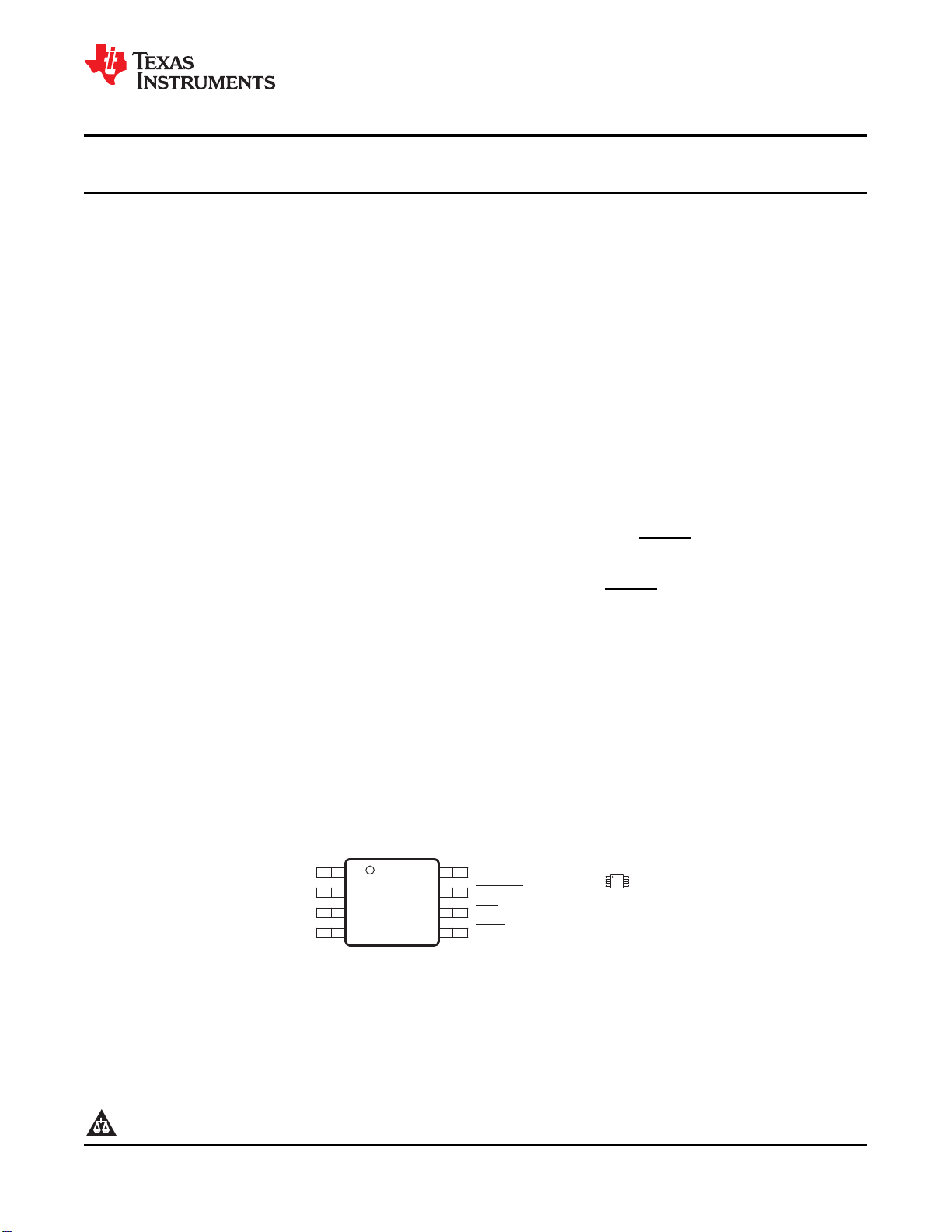
V
BAT
RESET
MR
PFO
8
7
6
5
1
2
3
4
V
OUT
V
DD
GND
PFI
DGK PACKAGE
(TOP VIEW)
ACTUAL SIZE
3,05 mm x 4,98 mm
TPS3619-33-EP, TPS3619-50-EP
TPS3620-33-EP, TPS3620-50-EP
www.ti.com
SGLS350C –JULY 2006–REVISED SEPTEMBER 2010
BACKUP-BATTERY SUPERVISORS FOR RAM RETENTION
Check for Samples: TPS3619-33-EP, TPS3619-50-EP, TPS3620-33-EP, TPS3620-50-EP
1
FEATURES
• Supply Current of 40 mA (Max)
• Battery-Supply Current of 100 nA (Max)
• Precision Supply-Voltage Monitor 3.3 V, 5 V,
and Other Options on Request
• Backup-Battery Voltage Can Exceed V
DD
• Power-On Reset Generator with Fixed 100-ms
Reset Delay Time
• Voltage Monitor for Power-Fail or Low-Battery
Monitoring
• Battery Freshness Seal (TPS3619)
• Pin-to-Pin Compatible With MAX819, MAX703,
and MAX704
• 8-Pin Mini Small-Outline Package (MSOP)
Package
SUPPORTS DEFENSE, AEROSPACE, AND MEDICAL APPLICATIONS
• Controlled Baseline
• One Assembly/Test Site
• One Fabrication Site
• Available in Military (–55°C/125°C)
Temperature Range
• Extended Product Life Cycle
• Extended Product-Change Notification
• Product Traceability
(1) Additional temperature ranges available - contact factory of –55°C to 125°C.
(1)
APPLICATIONS
• Fax Machines
• Set-Top Boxes
• Advanced Voice-Mail Systems
• Portable Battery-Powered Equipment
• Computer Equipment
• Advanced Modems
• Automotive Systems
• Portable Long-Time Monitoring Equipment
• Point-of-Sale Equipment
DESCRIPTION
The TPS3619 and TPS3620 families of supervisory
circuits monitor and control processor activity by
providing backup-battery switchover for data retention
of CMOS RAM.
During power on, RESET is asserted when the
supply voltage (VDDor V
V. Thereafter, the supply voltage supervisor monitors
VDDand keeps RESET output active as long as V
remains below the threshold voltage (VIT). An internal
timer delays the return of the output to the inactive
state (high) to ensure proper system reset. The delay
time starts after VDDhas risen above VIT. When the
supply voltage drops below VIT, the output becomes
active (low) again.
The product spectrum is designed for supply voltages
of 3.3 V and 5 V. The TPS3619 and TPS3620 are
available in an 8-pin MSOP package and are
characterized for operation over a temperature range
) becomes higher than 1.1
BAT
DD
1
PRODUCTION DATA information is current as of publication date.
Products conform to specifications per the terms of the Texas
Instruments standard warranty. Production processing does not
necessarily include testing of all parameters.
Please be aware that an important notice concerning availability, standard warranty, and use in critical applications of Texas
Instruments semiconductor products and disclaimers thereto appears at the end of this data sheet.
Copyright © 2006–2010, Texas Instruments Incorporated
V
DD
V
BAT
PFI
Backup
Battery
RESET
PFO
V
OUT
GND
R
x
R
y
External
Source
0.1 µF
Power
Supply
GND
RESET
I/O
V
CC
Switchover
Capacitor
0.1 µF
TPS3619
TPS3620
Microcontroller
or
Microprocessor
Manual
Reset
MR
Reel
Nominal Supply Voltage
Package
Functionality
Family
DGK EP
R
Temperature Range
Designator
TPS361 9 33 M
TPS3619-33-EP, TPS3619-50-EP
TPS3620-33-EP, TPS3620-50-EP
SGLS350C –JULY 2006–REVISED SEPTEMBER 2010
This integrated circuit can be damaged by ESD. Texas Instruments recommends that all integrated circuits be handled with
appropriate precautions. Failure to observe proper handling and installation procedures can cause damage.
ESD damage can range from subtle performance degradation to complete device failure. Precision integrated circuits may be more
susceptible to damage because very small parametric changes could cause the device not to meet its published specifications.
www.ti.com
TYPICAL OPERATING CIRCUIT
PACKAGE INFORMATION
T
A
–55°C to 125°C
(1) For the most current specifications and package information, see the Package Option Addendum located at the end of this data sheet or
see the TI web site at www.ti.com.
(2) Product Preview. Parameters in electrical characteristics are subject to change.
PRODUCT ORDERABLE PART NUMBER
TPS3619-33 BZP
TPS3619-50 TBD
TPS3620-33 BTY
TPS3620-50 TBD
PACKAGE TRANSPORT MEDIA,
MARKING QUANTITY
(1)
TPS3619-33MDGKEP
TPS3619-33MDGKREP Tape and reel, 2500
TPS3619-50MDGK
TPS3619-50MDGKREP
TPS3620-33MDGKTEP Tape and reel, 250
TPS3620-33MDGKREP Tape and reel, 2500
TPS3620-50MDGKTEP
TPS3620-50MDGKREP
(2)
(2)
(2)
(2)
(2)
Tube, 80
Tube, 80
Tape and reel, 2500
Tape and reel, 250
Tape and reel, 2500
2 Submit Documentation Feedback Copyright © 2006–2010, Texas Instruments Incorporated
Standard and Application-Specific Versions
DEVICE NAME NOMINAL VOLTAGE
TPS3619-33 DGK 3.3 V
TPS3619-50 DGK 5 V
TPS3620-33 DGK 3.3 V
TPS3620-50 DGK 5 V
Product Folder Link(s): TPS3619-33-EP TPS3619-50-EP TPS3620-33-EP TPS3620-50-EP
(1) For other threshold voltage versions, contact the local TI sales
office for availability and lead time.
(1)
, V
NOM
TPS3619-33-EP, TPS3619-50-EP
TPS3620-33-EP, TPS3620-50-EP
www.ti.com
SGLS350C –JULY 2006–REVISED SEPTEMBER 2010
Absolute Maximum Ratings
over operating free-air temperature (unless otherwise noted)
(2)
V
Supply voltage
Continuous output current, I
O
Continuous total power dissipation See Dissipation Ratings Table
Operating free-air temperature range, T
Storage temperature range, T
stg
A
Lead temperature soldering 1,6 mm (1/16 in) from case for 10 s 260°C
(1) Stresses beyond those listed under absolute maximum ratings may cause permanent damage to the device. These are stress ratings
only, and functional operation of the device at these or any other conditions beyond those indicated under recommended operating
conditions is not implied. Exposure to absolute-maximum-rated conditions for extended periods may affect device reliability.
(2) All voltage values are with respect to GND. For reliable operation, the device must not be continuously operated at 7 V for more than
t = 1000 h.
DD
MR and PFI pins
V
OUT
All other pins
(1)
UNIT
7 V
(2)
–0.3 V to (VDD+ 0.3 V)
400 mA
(2)
±10 mA
–55°C to 125°C
–65°C to 150°C
Dissipation Ratings
PACKAGE
DGK 470 mW 3.76 mW/°C 301 mW 241 mW 93.98 mW
TA< 25°C DERATING FACTOR TA= 70°C TA= 85°C TA= 125°C
POWER RATING ABOVE TA= 25°C POWER RATING POWER RATING POWER RATING
Recommended Operating Conditions
at specified temperature range
V
DD
V
BAT
V
I
V
IH
V
IL
I
O
Δt/ΔV Slew rate at VDDor V
T
A
Supply voltage 1.65 5.5 V
Battery supply voltage 1.5 5.5 V
Input voltage 0 VDD+ 0.3 V
High-level input voltage 0.7 × V
Low-level input voltage 0.3 × V
Continuous output current at V
OUT
Input transition rise and fall rate at MR 100 ns/V
BAT
Operating free-air temperature –55 125 °C
MIN MAX UNIT
DD
V
V
DD
300 mA
1 V/ms
Copyright © 2006–2010, Texas Instruments Incorporated Submit Documentation Feedback 3
Product Folder Link(s): TPS3619-33-EP TPS3619-50-EP TPS3620-33-EP TPS3620-50-EP
TPS3619-33-EP, TPS3619-50-EP
TPS3620-33-EP, TPS3620-50-EP
SGLS350C –JULY 2006–REVISED SEPTEMBER 2010
www.ti.com
Electrical Characteristics
over recommended operating conditions (unless otherwise noted)
PARAMETER TEST CONDITIONS MIN TYP MAX UNIT
RESET
V
High-level output voltage VDD= 1.8 V, IOH= –20 mA VDD– 0.3 V
OH
PFO VDD= 3.3 V, IOH= –80 mA VDD– 0.4
V
V
Low-level output voltage RESET, PFO VDD= 3.3 V, IOL= 2 mA 0.4 V
OL
Power-up reset voltage
res
(1)
Normal mode VDD– 150
V
OUT
Battery-backup mode
r
DS(on)
V
IT–
V
PFI
V
hys
VDDto V
V
BAT
Negative-going input threshold
voltage
Hysteresis 3.5 V < VIT< 5.5 V 60 mV
on resistance VDD= 5 V 0.6 1
OUT
to V
on resistance VDD= 3.3 V 8 20
OUT
TPS36XX-33 2.88 2.93 3.05
(2)
TPS36XX-50 4.46 4.55 4.64
V
IT
PFI 12
(3)
VBSW
I
I
I
I
I
I
C
High-level input current MR MR = 0.7 × VDD, VDD= 5 V –30 –76 mA
IH
Low-level input current MR MR = 0 V, VDD= 5 V –110 –255 mA
IL
Input current PFI –25 25 nA
I
Short-circuit current PFO PFO = 0 V VDD= 3.3 V –1.1 mA
OS
VDDsupply current mA
DD
(BAT)VBAT
I
supply current mA
Input capacitance VI= 0 V to 5 V 5 pF
(1) The lowest supply voltage at which RESET becomes active. t
(2) To ensure the best stability of the threshold voltage, a bypass capacitor (ceramic, 0.1 mF) should be placed near the supply terminals.
(3) For VDD< 1.6 V, V
switches to V
OUT
, regardless of V
BAT
VDD= 3.3 V, IOH= –2 mA VDD– 0.4
VDD= 5 V, IOH= –3 mA VDD– 0.4
VDD= 5 V, IOH= –120 mA VDD– 0.4
VDD= 1.8 V, IOL= –400 mA 0.2
VDD= 5 V, IOL= 3 mA 0.4
IOL= 20 mA, V
VDD> 1.1 V
I
= 8.5 mA, V
OUT
VDD= 1.8 V
I
= 125 mA, V
OUT
VDD= 3.3 V
I
= 190 mA, V
OUT
VDD= 5 V
I
= 0.5 mA, V
OUT
VDD= 0 V
I
= 7.5 mA, V
OUT
> 1.1 V or
BAT
= 0 V,
BAT
= 0 V,
BAT
= 0 V, mV
BAT
= 1.5 V,
BAT
= 3.3 V V
BAT
VDD– 50
VDD– 200
V
– 50
BAT
– 150
BAT
0.4 V
TA= –55°C to 125°C V
TA= –55°C to 125°C 1.13 1.15 1.185 V
1.65 V < VIT< 2.5 V 20
2.5 V < VIT< 3.5 V 40
VDD= 1.8 V 55
VDD= 1.8 V –0.3
VDD= 5 V –2.4
V
= V
OUT
DD
V
= V
OUT
BAT
V
= V
OUT
DD
V
= V
OUT
BAT
≥ 15 ms/V.
r,VDD
.
BAT
–0.1 0.1
40
40
0.5
Ω
4 Submit Documentation Feedback Copyright © 2006–2010, Texas Instruments Incorporated
Product Folder Link(s): TPS3619-33-EP TPS3619-50-EP TPS3620-33-EP TPS3620-50-EP
V
IT
V
BAT
V
DD
V
OUT
RESET
t
d
t
t
t
t
d
TPS3619-33-EP, TPS3619-50-EP
TPS3620-33-EP, TPS3620-50-EP
www.ti.com
SGLS350C –JULY 2006–REVISED SEPTEMBER 2010
Timing Requirements
at RL= 1 MΩ, CL= 50 pF, TA= 25°C
PARAMETER TEST CONDITIONS MIN MAX UNIT
t
w
Pulse width
at V
DD
at MR VDD= VIT+ 0.2 V, VIL= 0.3 x VDD, VIH= 0.7 × V
VIH= VIT+ 0.2 V, VIL= VIT– 0.2 V 6 ms
DD
100 ns
Switching Characteristics
at RL= 1 MΩ, CL= 50 pF, TA= –55°C to 125°C
PARAMETER TEST CONDITIONS MIN TYP MAX UNIT
t
Delay time 60 100 140 ms
d
VDDto RESET VIL= VIT– 0.4 V, VIH= VIT+ 0.4 V 2 5
Propagation (delay) time, PFI to PFO delay VIL= V
t
PHL
high-to-low-level output
MR to RESET 0.1 1
VDD≥ VIT+ 0.2 V, MR ≥ 0.7 × VDD,
See timing diagram
– 0.35 V, VIH= V
PFI
PFI
VDD≥ VIT+ 0.2 V, VIL= 0.3 × VDD,
VIH= 0.7 × V
DD
Timing Diagram
+ 0.35 V 3 5
ms
Copyright © 2006–2010, Texas Instruments Incorporated Submit Documentation Feedback 5
Product Folder Link(s): TPS3619-33-EP TPS3619-50-EP TPS3620-33-EP TPS3620-50-EP
TPS3619-33-EP, TPS3619-50-EP
TPS3620-33-EP, TPS3620-50-EP
SGLS350C –JULY 2006–REVISED SEPTEMBER 2010
Table 1. FUNCTION TABLE
VDD> V
0 0 L V
0 0 H V
0 1 L V
0 1 H V
1 0 L V
1 0 H V
1 1 L V
1 1 H V
IT
VDD> V
BAT
PFI > V
PFI
0 L
1 H
CONDITION: VDD> VDD(MIN)
TERMINAL FUNCTIONS
TERMINAL
NAME NO.
GND 3 I Ground
MR 6 I Manual reset
PFI 4 I Power-fail comparator input
PFO 5 O Power-fail comparator output
RESET 7 O Active-low reset
V
BAT
V
DD
V
OUT
8 I Backup battery
2 I Supply input voltage
1 O Supply output voltage
I/O DESCRIPTION
MR V
PFO
OUT
BAT
BAT
DD
DD
DD
DD
DD
DD
www.ti.com
RESET
L
L
L
L
L
H
L
H
6 Submit Documentation Feedback Copyright © 2006–2010, Texas Instruments Incorporated
Product Folder Link(s): TPS3619-33-EP TPS3619-50-EP TPS3620-33-EP TPS3620-50-EP

_
+
Switch
Control
Reference
Voltage
of 1.15 V
_
+
RESET
Logic
+
Timer
V
BAT
V
DD
PFI
V
OUT
RESET
PFO
MR
_
+
TPS3619-33-EP, TPS3619-50-EP
TPS3620-33-EP, TPS3620-50-EP
www.ti.com
SGLS350C –JULY 2006–REVISED SEPTEMBER 2010
FUNCTIONAL BLOCK DIAGRAM
Copyright © 2006–2010, Texas Instruments Incorporated Submit Documentation Feedback 7
Product Folder Link(s): TPS3619-33-EP TPS3619-50-EP TPS3620-33-EP TPS3620-50-EP

500
600
700
800
900
1000
50 75 100 125 150 175 200
TA = 85°C
TA = 25°C
TA = 0°C
TA = −40°C
− Static Drain-Source On-State Resistance − m
V
DD
= 3.3 V
V
BAT
= GND
IO − Output Current − mA
r
DS(on)
Ω
5
10
15
20
2.5 4.5 6.5 8.5 10.5 12.5 14.5
TA = 85°C
TA = 25°C
TA = 0°C
TA = −40°C
− Static Drain-Source On-State Resistance −
IO − Output Current − mA
r
DS(on)
Ω
V
BAT
= 3.3 V
7.5
12.5
17.5
0.995
0.996
0.997
0.998
0.999
1
1.001
−40 −30 −20 −10 0 10 20 30 40 50 60 70 80
− Normalized Threshold Voltage at RESET − V
V
IT
TA − Free-Air Temperature − °C
0
5
10
15
20
25
30
0 1 2 3 4 5 6
TA = −40°C
TA = 25°C
TA = 85°C
TA = 0°C
− Supply Current −I
DD
Aµ
VDD − Supply Voltage − V
V
BAT
Mode
V
BAT
= 2.6 V
V
DD
Mode
V
BAT
= GND
or
TPS3619-33-EP, TPS3619-50-EP
TPS3620-33-EP, TPS3620-50-EP
SGLS350C –JULY 2006–REVISED SEPTEMBER 2010
STATIC DRAIN-SOURCE ON-STATE RESISTANCE STATIC DRAIN-SOURCE ON-STATE RESISTANCE
(VDDto V
) (V
OUT
vs vs
OUTPUT CURRENT OUTPUT CURRENT
TYPICAL CHARACTERISTICS
BAT
to V
OUT
www.ti.com
)
SUPPLY CURRENT NORMALIZED THRESHOLD AT RESET
SUPPLY VOLTAGE FREE-AIR TEMPERATURE
8 Submit Documentation Feedback Copyright © 2006–2010, Texas Instruments Incorporated
Product Folder Link(s): TPS3619-33-EP TPS3619-50-EP TPS3620-33-EP TPS3620-50-EP
Figure 1. Figure 2.
vs vs
Figure 3. Figure 4.

0
1
2
3
4
5
6
−35−30−25−20−15−10−−50
TA = −40°C
TA = 85°C
TA = 0°C
TA = 25°C
IOH − High-Level Output Current − mA
VDD = 5 V
V
BAT
= GND
V
OH
– High-Level Output Voltage at RESET – V
4.5
4.6
4.7
4.8
4.9
5
5.1
−5−4.5−4−3.5−3−2.5−2−1.5−1−0.50
TA = −40°C
TA = 25°C
TA = 85°C
TA = 0°C
IOH − High-Level Output Current − mA
VDD = 5 V
V
BAT
= GND
Expanded View
V
OH
– High-Level Output Voltage at RESET – V
0
1
2
3
4
5
6
−2.5−2−1.5−1−0.50
TA = −40°C
TA = 25°C
TA = 85°C
TA = 0°C
IOH − High-Level Output Current − mA
VDD = 5.5 V
PFI = 1.4 V
V
BAT
= GND
V
OH
– High-Level Output Voltage at PFO – V
5.10
5.15
5.20
5.25
5.30
5.35
5.40
5.45
5.50
5.55
−200−180−160−140−120−100−80−60−40−200
TA = −40°C
TA = 25°C
TA = 85°C
TA = 0°C
IOH − High-Level Output Current − µA
VDD = 5.5 V
PFI = 1.4 V
V
BAT
= GND
Expanded View
V
OH
– High-Level Output Voltage at PFO – V
TPS3619-33-EP, TPS3619-50-EP
TPS3620-33-EP, TPS3620-50-EP
www.ti.com
SGLS350C –JULY 2006–REVISED SEPTEMBER 2010
TYPICAL CHARACTERISTICS (continued)
HIGH-LEVEL OUTPUT VOLTAGE AT RESET HIGH-LEVEL OUTPUT VOLTAGE AT RESET
vs vs
HIGH-LEVEL OUTPUT CURRENT HIGH-LEVEL OUTPUT CURRENT
Figure 5. Figure 6.
HIGH-LEVEL OUTPUT VOLTAGE AT PFO HIGH-LEVEL OUTPUT VOLTAGE AT PFO
vs vs
HIGH-LEVEL OUTPUT CURRENT HIGH-LEVEL OUTPUT CURRENT
Figure 7. Figure 8.
Product Folder Link(s): TPS3619-33-EP TPS3619-50-EP TPS3620-33-EP TPS3620-50-EP
Copyright © 2006–2010, Texas Instruments Incorporated Submit Documentation Feedback 9

0
0.5
1
1.5
2
2.5
3
3.5
0 5 10 15 20 25
TA = 25°C
TA = 85°C
TA = 0°C
TA = −40°C
IOL − Low-Level Output Current − mA
VDD = 3.3 V
V
BAT
= GND
V
OL
– Low-Level Output Voltage at RESET – V
0
100
200
300
400
500
0
1 2 3 4 5
TA = −40°C
TA = 25°C
TA = 85°C
TA = 0°C
IOL − Low-Level Output Current − mA
VDD = 3.3 V
V
BAT
= GND
Expanded View
V
OL
– Low-Level Output Voltage at RESET – mV
0
1
2
3
4
5
6
7
8
9
10
0 0.1 0.2 0.3 0.4 0.5 0.6 0.7 0.8 0.9
Minimum Pulse Duration at − V
DD
Threshold Overdrive at VDD − V
1
sµ
0.6
1
1.4
1.8
2.2
2.6
3
3.4
3.8
4.2
4.6
5
0 0.1 0.2 0.3 0.4 0.5 0.6 0.7 0.8 0.9
1
Minimum Pulse Duration at PFI −
Threshold Overdrive at PFI − V
VDD = 1.65 V
sµ
TPS3619-33-EP, TPS3619-50-EP
TPS3620-33-EP, TPS3620-50-EP
SGLS350C –JULY 2006–REVISED SEPTEMBER 2010
TYPICAL CHARACTERISTICS (continued)
LOW-LEVEL OUTPUT VOLTAGE AT RESET LOW-LEVEL OUTPUT VOLTAGE AT RESET
vs vs
LOW-LEVEL OUTPUT CURRENT LOW-LEVEL OUTPUT CURRENT
Figure 9. Figure 10.
www.ti.com
MINIMUM PULSE DURATION AT V
THRESHOLD OVERDRIVE AT V
10 Submit Documentation Feedback Copyright © 2006–2010, Texas Instruments Incorporated
Product Folder Link(s): TPS3619-33-EP TPS3619-50-EP TPS3620-33-EP TPS3620-50-EP
DD
MINIMUM PULSE DURATION AT PFI
vs vs
DD
THRESHOLD OVERDRIVE AT PFI
Figure 11. Figure 12.

TPS3619-33-EP, TPS3619-50-EP
TPS3620-33-EP, TPS3620-50-EP
www.ti.com
SGLS350C –JULY 2006–REVISED SEPTEMBER 2010
DETAILED DESCRIPTION
Battery Freshness Seal (TPS3619)
The battery freshness seal of the TPS3619 family disconnects the backup battery from internal circuitry until it is
needed. This function prevents the backup battery from being discharged until the final product is put to use. The
following steps explain how to enable the freshness seal mode.
1. Connect V
BAT(VBAT
> V
BAT
min)
2. Ground PFO
3. Connect PFI to VDD(PFI = VDD)
4. Connect VDDto power supply (VDD> VIT) and retain for 5 ms < t < 35 ms
The battery freshness seal mode is removed automatically by the positive-going edge of RESET when VDDis
applied.
Power-Fail Input/Output Comparator (PFI and PFO)
An additional comparator is provided to monitor voltages other than the nominal supply voltage. The PFI is
compared with an internal voltage reference of 1.15 V. If the input voltage falls below the power-fail threshold
(V
returns to high. By connecting two external resistors, it is possible to supervise any voltages above V
sum of both resistors should be about 1 MΩ, to minimize power consumption and also to ensure that the current
in the PFI pin can be ignored, compared with the current through the resistor network. The tolerance of the
external resistors should be not more than 1%, to ensure minimal variation of sensed voltage. If the power-fail
comparator is unused, PFI should be connected to ground and PFO left unconnected.
) of 1.15 V (typ), the PFO goes low. If V
IT(PFI)
goes above V
IT(PFI)
plus about 12-mV hysteresis, the output
(PFI)
(PFI)
. The
Backup-Battery Switchover
In case of a brownout or power failure, it may be necessary to preserve the contents of RAM. If a backup battery
is installed at V
order to allow the backup battery (e.g., a 3.6-V lithium cell) to have a higher voltage than VDD, these supervisors
do not connect V
when VDDfalls below the VITand V
until VDDcrosses V
when VDDcrosses the reset threshold.
, the device automatically switches the connected RAM to backup power when VDDfails. In
BAT
BAT
to V
BAT
OUT
when V
is greater than VDD. V
BAT
is greater than VDD. When VDDrecovers, switchover is deferred, either
BAT
or until VDDrises above VIT. V
only connects to V
BAT
connects to VDDthrough a 1-Ω (max) PMOS switch
OUT
(through a 15-Ω switch)
OUT
Table 2. FUNCTION TABLE
VDD> V
BAT
1 1 V
1 0 V
0 1 V
0 0 V
VDD> V
IT
V
OUT
DD
DD
DD
BAT
Copyright © 2006–2010, Texas Instruments Incorporated Submit Documentation Feedback 11
Product Folder Link(s): TPS3619-33-EP TPS3619-50-EP TPS3620-33-EP TPS3620-50-EP

Undefined
VBSW Hysteresis
V
BAT
Mode
VDD Mode
VIT Hysteresis
– Normal Supply Voltage – VV
DD
V
BAT
– Backup-Battery Supply Voltage – V
TPS3619-33-EP, TPS3619-50-EP
TPS3620-33-EP, TPS3620-50-EP
SGLS350C –JULY 2006–REVISED SEPTEMBER 2010
Figure 13. Normal Supply Voltage vs Backup-Battery Supply Voltage
www.ti.com
12 Submit Documentation Feedback Copyright © 2006–2010, Texas Instruments Incorporated
Product Folder Link(s): TPS3619-33-EP TPS3619-50-EP TPS3620-33-EP TPS3620-50-EP

PACKAGE OPTION ADDENDUM
www.ti.com
10-Dec-2020
PACKAGING INFORMATION
Orderable Device Status
TPS3619-33MDGKREP ACTIVE VSSOP DGK 8 2500 RoHS & Green NIPDAU Level-1-260C-UNLIM -55 to 125 BZP
TPS3620-33MDGKREP ACTIVE VSSOP DGK 8 2500 RoHS & Green NIPDAU Level-1-260C-UNLIM -55 to 125 BTY
TPS3620-33MDGKTEP ACTIVE VSSOP DGK 8 250 RoHS & Green NIPDAU Level-1-260C-UNLIM -55 to 125 BTY
V62/06670-01XE ACTIVE VSSOP DGK 8 2500 RoHS & Green NIPDAU Level-1-260C-UNLIM -55 to 125 BZP
V62/06670-03XE ACTIVE VSSOP DGK 8 2500 RoHS & Green NIPDAU Level-1-260C-UNLIM -55 to 125 BTY
(1)
The marketing status values are defined as follows:
ACTIVE: Product device recommended for new designs.
LIFEBUY: TI has announced that the device will be discontinued, and a lifetime-buy period is in effect.
NRND: Not recommended for new designs. Device is in production to support existing customers, but TI does not recommend using this part in a new design.
PREVIEW: Device has been announced but is not in production. Samples may or may not be available.
OBSOLETE: TI has discontinued the production of the device.
Package Type Package
(1)
Drawing
Pins Package
Qty
Eco Plan
(2)
Lead finish/
Ball material
(6)
MSL Peak Temp
(3)
Op Temp (°C) Device Marking
(4/5)
(2)
RoHS: TI defines "RoHS" to mean semiconductor products that are compliant with the current EU RoHS requirements for all 10 RoHS substances, including the requirement that RoHS substance
do not exceed 0.1% by weight in homogeneous materials. Where designed to be soldered at high temperatures, "RoHS" products are suitable for use in specified lead-free processes. TI may
reference these types of products as "Pb-Free".
RoHS Exempt: TI defines "RoHS Exempt" to mean products that contain lead but are compliant with EU RoHS pursuant to a specific EU RoHS exemption.
Green: TI defines "Green" to mean the content of Chlorine (Cl) and Bromine (Br) based flame retardants meet JS709B low halogen requirements of <=1000ppm threshold. Antimony trioxide based
flame retardants must also meet the <=1000ppm threshold requirement.
(3)
MSL, Peak Temp. - The Moisture Sensitivity Level rating according to the JEDEC industry standard classifications, and peak solder temperature.
(4)
There may be additional marking, which relates to the logo, the lot trace code information, or the environmental category on the device.
(5)
Multiple Device Markings will be inside parentheses. Only one Device Marking contained in parentheses and separated by a "~" will appear on a device. If a line is indented then it is a continuation
of the previous line and the two combined represent the entire Device Marking for that device.
(6)
Lead finish/Ball material - Orderable Devices may have multiple material finish options. Finish options are separated by a vertical ruled line. Lead finish/Ball material values may wrap to two
lines if the finish value exceeds the maximum column width.
Samples
Addendum-Page 1

PACKAGE OPTION ADDENDUM
www.ti.com
Important Information and Disclaimer:The information provided on this page represents TI's knowledge and belief as of the date that it is provided. TI bases its knowledge and belief on information
provided by third parties, and makes no representation or warranty as to the accuracy of such information. Efforts are underway to better integrate information from third parties. TI has taken and
continues to take reasonable steps to provide representative and accurate information but may not have conducted destructive testing or chemical analysis on incoming materials and chemicals.
TI and TI suppliers consider certain information to be proprietary, and thus CAS numbers and other limited information may not be available for release.
10-Dec-2020
In no event shall TI's liability arising out of such information exceed the total purchase price of the TI part(s) at issue in this document sold by TI to Customer on an annual basis.
Addendum-Page 2

PACKAGE MATERIALS INFORMATION
www.ti.com 3-Aug-2017
TAPE AND REEL INFORMATION
*All dimensions are nominal
Device Package
TPS3619-33MDGKREP VSSOP DGK 8 2500 330.0 12.4 5.3 3.4 1.4 8.0 12.0 Q1
TPS3620-33MDGKREP VSSOP DGK 8 2500 330.0 12.4 5.3 3.4 1.4 8.0 12.0 Q1
TPS3620-33MDGKTEP VSSOP DGK 8 250 177.8 12.4 5.3 3.4 1.4 8.0 12.0 Q1
Type
Package
Drawing
Pins SPQ Reel
Diameter
(mm)
Reel
Width
W1 (mm)
A0
(mm)B0(mm)K0(mm)P1(mm)W(mm)
Quadrant
Pin1
Pack Materials-Page 1

PACKAGE MATERIALS INFORMATION
www.ti.com 3-Aug-2017
*All dimensions are nominal
Device Package Type Package Drawing Pins SPQ Length (mm) Width (mm) Height (mm)
TPS3619-33MDGKREP VSSOP DGK 8 2500 358.0 335.0 35.0
TPS3620-33MDGKREP VSSOP DGK 8 2500 358.0 335.0 35.0
TPS3620-33MDGKTEP VSSOP DGK 8 250 202.0 201.0 28.0
Pack Materials-Page 2


IMPORTANT NOTICE AND DISCLAIMER
TI PROVIDES TECHNICAL AND RELIABILITY DATA (INCLUDING DATASHEETS), DESIGN RESOURCES (INCLUDING REFERENCE
DESIGNS), APPLICATION OR OTHER DESIGN ADVICE, WEB TOOLS, SAFETY INFORMATION, AND OTHER RESOURCES “AS IS”
AND WITH ALL FAULTS, AND DISCLAIMS ALL WARRANTIES, EXPRESS AND IMPLIED, INCLUDING WITHOUT LIMITATION ANY
IMPLIED WARRANTIES OF MERCHANTABILITY, FITNESS FOR A PARTICULAR PURPOSE OR NON-INFRINGEMENT OF THIRD
PARTY INTELLECTUAL PROPERTY RIGHTS.
These resources are intended for skilled developers designing with TI products. You are solely responsible for (1) selecting the appropriate
TI products for your application, (2) designing, validating and testing your application, and (3) ensuring your application meets applicable
standards, and any other safety, security, or other requirements. These resources are subject to change without notice. TI grants you
permission to use these resources only for development of an application that uses the TI products described in the resource. Other
reproduction and display of these resources is prohibited. No license is granted to any other TI intellectual property right or to any third
party intellectual property right. TI disclaims responsibility for, and you will fully indemnify TI and its representatives against, any claims,
damages, costs, losses, and liabilities arising out of your use of these resources.
TI’s products are provided subject to TI’s Terms of Sale (www.ti.com/legal/termsofsale.html) or other applicable terms available either on
ti.com or provided in conjunction with such TI products. TI’s provision of these resources does not expand or otherwise alter TI’s applicable
warranties or warranty disclaimers for TI products.
Mailing Address: Texas Instruments, Post Office Box 655303, Dallas, Texas 75265
Copyright © 2020, Texas Instruments Incorporated
 Loading...