

www.ti.com
1
2
3
4
8
7
6
5
SENSE1
SENSE2
SENSE3
GND
V
DD
MR
RESET
RESET
D OR DGN PACKAGE
(TOP VIEW)
SENSE 1
SENSE 2 RESET
TPS3307−33
SENSE 3
V
DD
GND
100nF
RESET
V
DD
GND
3.3V5V2.5V
470kΩ
620kΩ
• Applications using DSPs,
Microcontrollers or Microprocessors
w Industrial Equipment
w Programmable Controls
w Automotive Systems
w Portable/Battery Powered Equipment
w Intelligent Instruments
w Wireless Communication Systems
w Notebook/Desktop Computers
MSP430C325
TPS3307-18 , TPS3307-25 , TPS3307-33
SLVS199C – DECEMBER 1998 – REVISED DECEMBER 2006
TRIPLE PROCESSOR SUPERVISORS
FEATURES
• Triple Supervisory Circuits for DSP and
Processor-Based Systems
• Power-On Reset Generator With Fixed Delay
Time of 200ms, No External Capacitor Needed
• Temperature-Compensated Voltage Reference
• Maximum Supply Current of 40 µ A
• Supply Voltage Range: 2V to 6V
• Defined RESET Output From V
• MSOP-8 and SO-8 Packages
• Temperature Range : – 40 ° C to +85 ° C
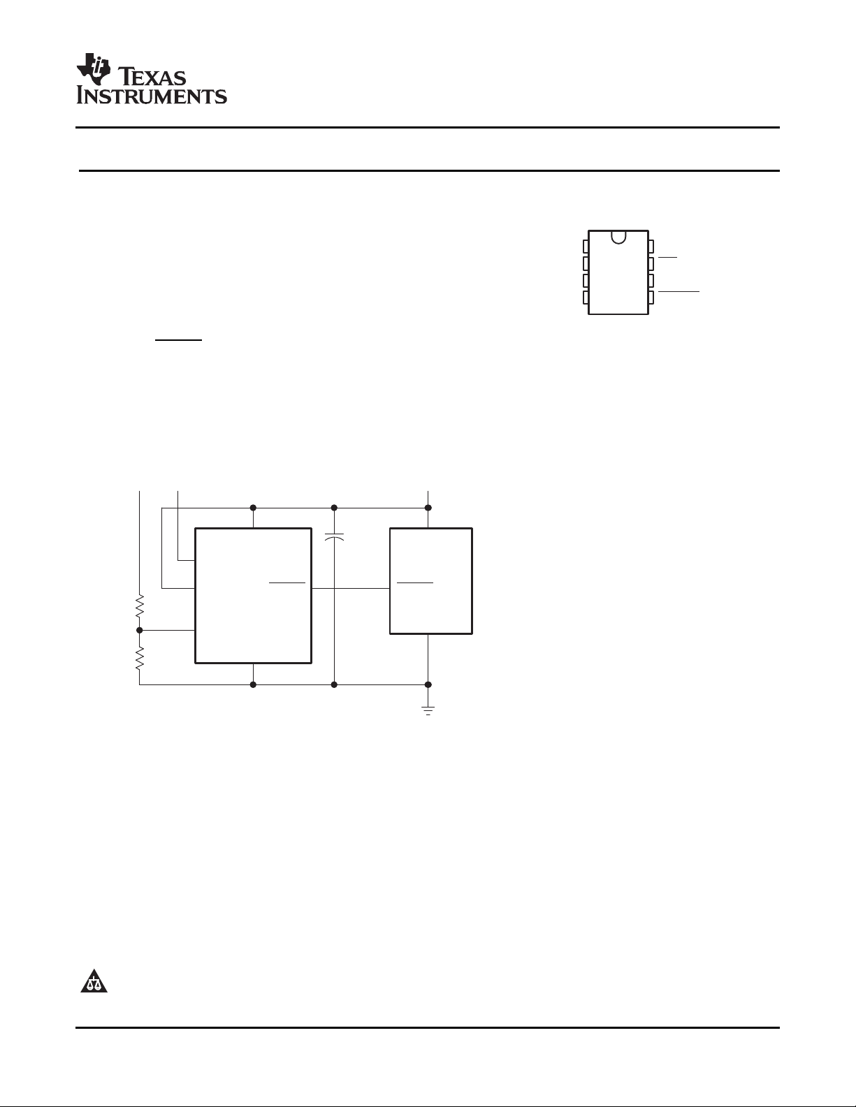
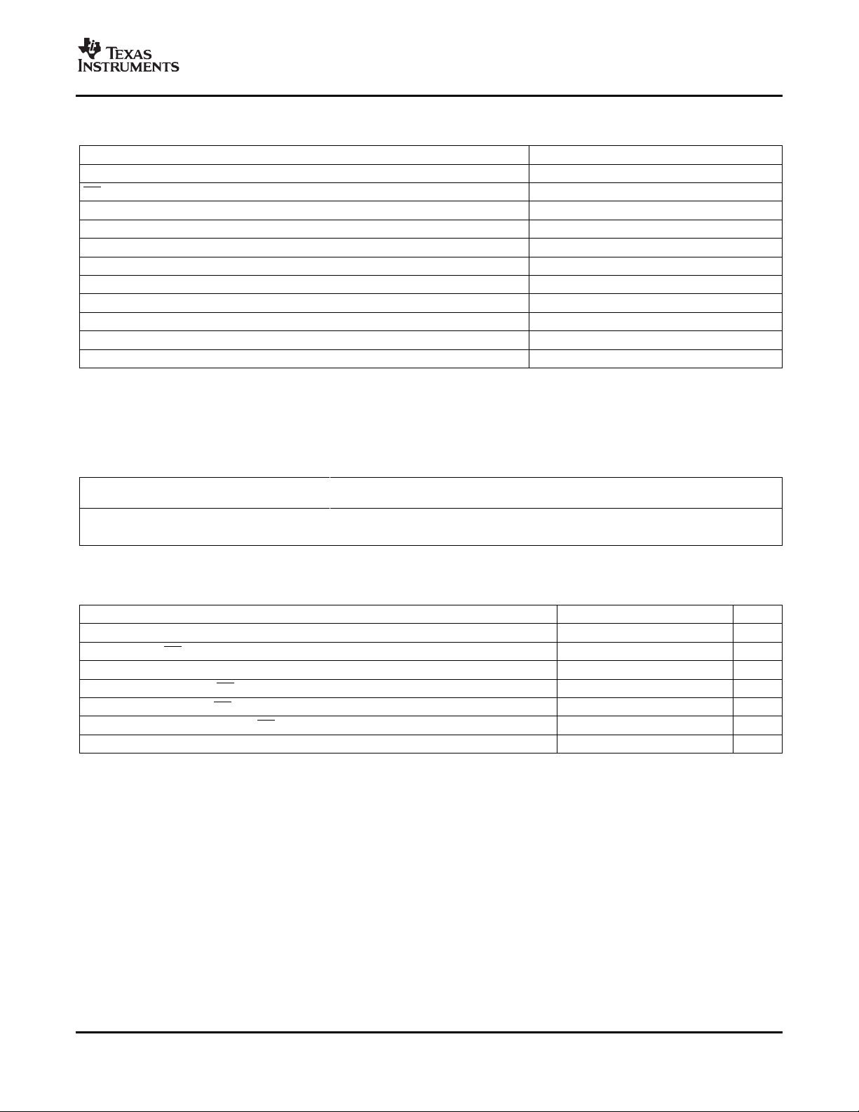
TYPICAL APPLICATIONS
Figure 1 lists some of the typical applications for the TPS3307 family, and a schematic diagram for a
processor-based system application. This application uses TI part numbers TPS3307-33 and MSP430C325 .
≥ 1.1V
DD
Figure 1. Applications Using the TPS3307 Family
DESCRIPTION
The TPS3307 family is a series of micropower supply voltage supervisors designed for circuit initialization
primarily in DSP and processor-based systems, which require more than one supply voltage.
The product spectrum of the TPS3307-xx is designed for monitoring three independent supply voltages:
3.3V/1.8V/adj, 3.3V/2.5V/adj or 3.3V/5V/adj. The adjustable SENSE input allows the monitoring of any supply
voltage >1.25V.
The various supply voltage supervisors are designed to monitor the nominal supply voltage as shown in the
following supply voltage monitoring table .
PowerPAD is a trademark of Texas Instruments.
All other trademarks are the property of their respective owners.
PRODUCTION DATA information is current as of publication date.
Products conform to specifications per the terms of the Texas
Instruments standard warranty. Production processing does not
necessarily include testing of all parameters.
Please be aware that an important notice concerning availability, standard warranty, and use in critical applications of Texas
Instruments semiconductor products and disclaimers thereto appears at the end of this data sheet.
Copyright © 1998–2006, Texas Instruments Incorporated
www.ti.com
TPS3307-18 , TPS3307-25 , TPS3307-33
SLVS199C – DECEMBER 1998 – REVISED DECEMBER 2006
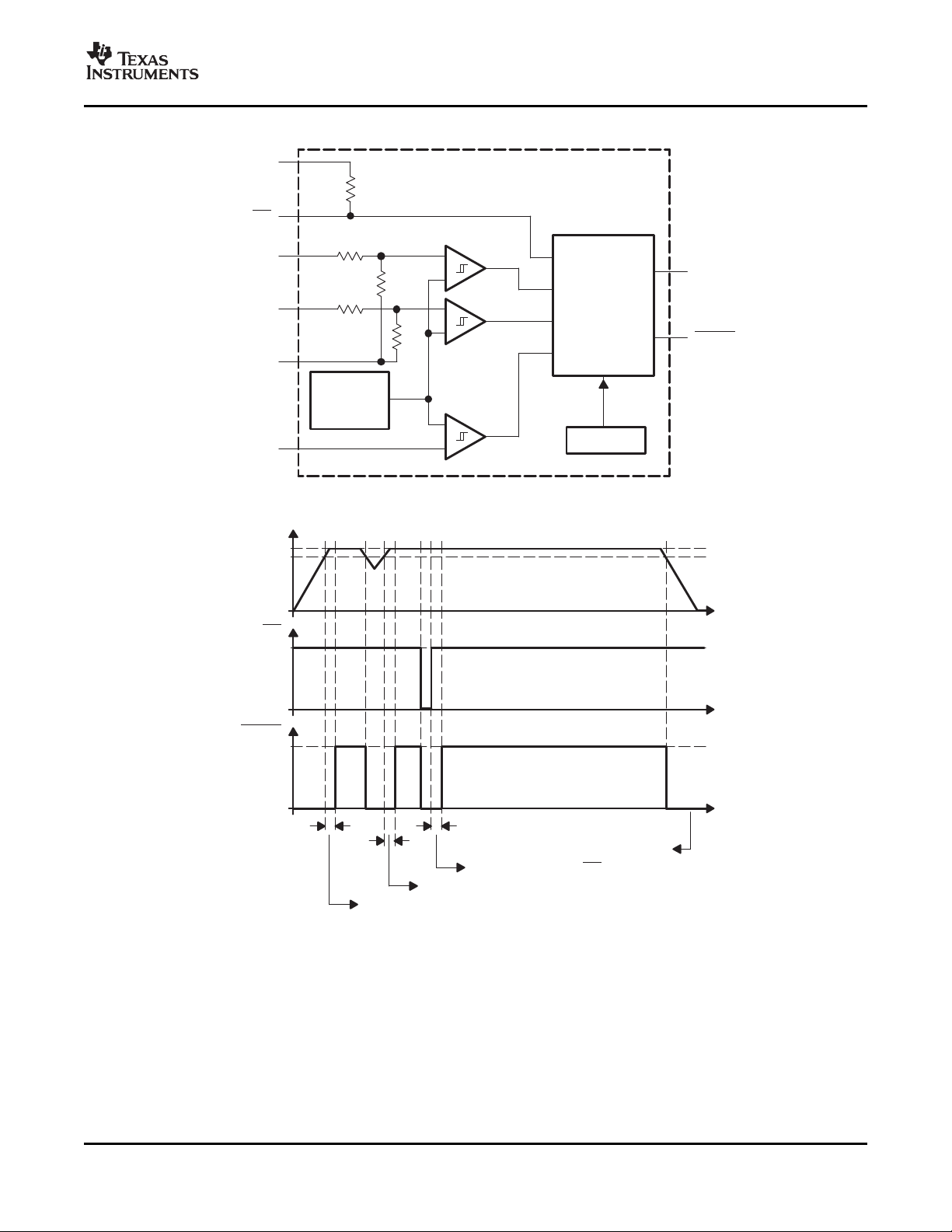
During power-on, RESET is asserted when the supply voltage V
becomes higher than 1.1V. Thereafter, the
DD
supply voltage supervisor monitors the SENSE n inputs and keeps RESET active as long as SENSE n remain
below the threshold voltage V
.
IT+
An internal timer delays the return of the RESET output to the inactive state (high) to ensure proper system
reset. The delay time, t
When the voltage at any SENSE input drops below the threshold voltage V
= 200ms, starts after all SENSE n inputs have risen above the threshold voltage V
d (typ)
, the RESET output becomes
IT–
active (low) again.
The TPS3307-xx family of devices incorporates a manual reset input, MR. A low level at MR causes RESET to
become active. In addition to the active-low RESET output, the TPS3307-xx family includes an active-high
RESET output.
The devices are available in either 8-pin MSOP or standard 8-pin SO packages.
The TPS3307-xx devices are characterized for operation over a temperature range of –40 ° C to +85 ° C.
SUPPLY VOLTAGE MONITORING
DEVICE
TPS3307-18 3.3V 1.8V User defined 2.93V 1.68V 1.25V
TPS3307-25 3.3V 2.5V User defined 2.93V 2.25V 1.25V
TPS3307-33 5V 3.3V User defined 4.55V 2.93V 1.25V
(1) The actual sense voltage has to be adjusted by an external resistor divider according to the application requirements.
T
A
–40 ° C to +85 ° C TPS3307-25D TPS3307-25DGN TIAAQ TPS3307-25Y
(1) For the most current package and ordering information, see the Package Option Addendum at the end of this document, or see the TI
website at www.ti.com .
NOMINAL SUPERVISED VOLTAGE THRESHOLD VOLTAGE (TYP)
SENSE1 SENSE2 SENSE3 SENSE1 SENSE2 SENSE3
AVAILABLE OPTIONS
PACKAGED DEVICES
SMALL OUTLINE
(D)
TPS3307-18D TPS3307-18DGN TIAAP TPS3307-18Y
TPS3307-33D TPS3307-33DGN TIAAR TPS3307-33Y
PowerPAD™
µ -SMALL OUTLINE
(DGN)
(1)
MARKING CHIP FORM
DGN PACKAGE (Y)
(1)
(1)
(1)
Function/Truth Tables
MR SENSE1 > V
L X
H 0 0 0 L H
H 0 0 1 L H
H 0 1 0 L H
H 0 1 1 L H
H 1 0 0 L H
H 1 0 1 L H
H 1 1 0 L H
H 1 1 1 H L
(1) X = Don't care
IT1
(1)
SENSE2 > V
(1)
X
IT2
SENSE3 > V
IT3
X L H
RESET RESET
.
IT+
2
Submit Documentation Feedback
www.ti.com
_
+
_
+
_
+
R4
R2
R1
R3
Reference
Voltage
of 1.25V
RESET
Logic + Timer
Oscillator
14 kΩ
V
DD
MR
SENSE 1
SENSE 2
GND
SENSE 3
RESET
RESET
TPS3307
t
d
t
d
t
d
RESET Because of SENSE Below V
IT
RESET Because of MR
RESET Because of SENSE Below V
IT–
RESET Because of SENSE Below V
IT–
SENSEn
V
(nom)
V
IT–
MR
1
0
1
0
RESET
t
t
t
Functional Block Diagram
Timing Diagram
TPS3307-18 , TPS3307-25 , TPS3307-33
SLVS199C – DECEMBER 1998 – REVISED DECEMBER 2006
Submit Documentation Feedback
3
www.ti.com
56
48
TPS3307Y
(1)
(2)
(3)
(5)
(6)
CHIP THICKNESS: 10 TYPICAL
BONDING PADS: 4 × 4 MINIMUM
T
J
max = 150°C
TOLERANCES ARE ±10%.
ALL DIMENSIONS ARE IN MILS
(4)
(7)
(8)
TPS3307-18 , TPS3307-25 , TPS3307-33
SLVS199C – DECEMBER 1998 – REVISED DECEMBER 2006
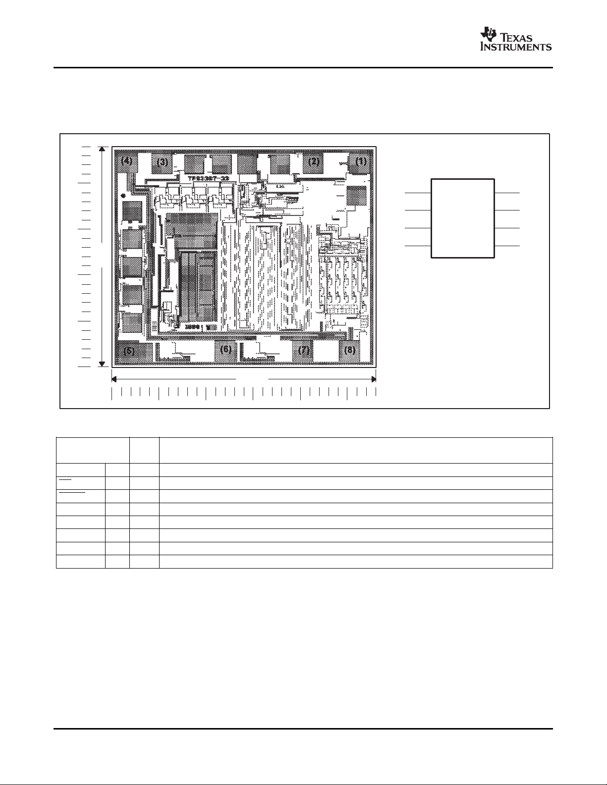
TPS3307Y Chip Information
These chips, when properly assembled, display characteristics similar to those of the TPS3307. Thermal
compression or ultrasonic bonding may take place on the doped aluminium bonding pads. The chips may be
mounted with conductive epoxy or a gold-silicon preform.
TERMINAL
NAME NO.
GND 4 Ground
MR 7 I Manual reset
RESET 5 O Active-low reset output
RESET 6 O Active-high reset output
SENSE1 1 I Sense voltage input 1
SENSE2 2 I Sense voltage input 2
SENSE3 3 I Sense voltage input 3
V
DD
I/O DESCRIPTION
8 Supply voltage
Table 2. Terminal Functions
4
Submit Documentation Feedback
www.ti.com
TPS3307-18 , TPS3307-25 , TPS3307-33
SLVS199C – DECEMBER 1998 – REVISED DECEMBER 2006
Absolute Maximum Ratings
Over operating free-air temperature range (unless otherwise noted).
Supply voltage, V
MR pin –0.3V to V
All other pins
Maximum low output current, I
Maximum high output current, I
Input clamp current, IIK(VI< 0 or VI> VDD) ± 20mA
Output clamp current, IOK(V
Continuous total power dissipation See Dissipation Rating Table
Operating free-air temperature range, T
Storage temperature range, T
Soldering temperature +260 ° C
(1) Stresses beyond those listed under absolute maximum ratings may cause permanent damage to the device. These are stress ratings
only, and functional operation of the device at these or any other conditions beyond those indicated under recommended operating
conditions is not implied. Exposure to absolute-maximum-rated conditions for extended periods may affect device reliability.
(2) All voltage values are with respect to GND. For reliable operation the device must not be operated at 7V for more than t = 1000h
continuously.
(2)
DD
(2)
OL
OH
< 0 or VO> VDD) ± 20mA
O
stg
(1)
UNIT
7V
+0.3V
DD
–0.3V to 7V
5mA
–5mA
A
–40 ° C to +85 ° C
–65 ° C to +150 ° C
Dissipation Rating Table
PACKAGE
DGN 2.14W 17.1mW/ ° C 1.37W 1.11W
D 725mW 5.8mW/ ° C 464mW 377mW
TA≤ +25 ° C DERATING FACTOR TA= +70 ° C TA= +85 ° C
POWER RATING ABOVE TA= +25 ° C POWER RATING POWER RATING
Recommended Operating Conditions
At specified temperature range.
MIN MAX UNIT
Supply voltage, V
Input voltage at MR and SENSE3, V
Input voltage at SENSE1 and SENSE2, V
High-level input voltage at MR, V
Low-level input voltage at MR, V
DD
I
I
IH
IL
Input transition rise and fall rate at MR, ∆ t/ ∆ V 50 ns/V
Operating free-air temperature range, T
A
2 6 V
0 V
0.7 x V
0 (V
DD
+0.3)V
DD
–40 +85 ° C
+ 0.3 V
DD
/1.25V V
IT
0.3 × V
V
V
DD
Submit Documentation Feedback
5
www.ti.com
TPS3307-18 , TPS3307-25 , TPS3307-33
SLVS199C – DECEMBER 1998 – REVISED DECEMBER 2006
Electrical Characteristics
Over recommended operating free-air temperature range (unless otherwise noted).
PARAMETER TEST CONDITIONS MIN TYP MAX UNIT
V
= 2V to 6V, IOH= –20 µ A V
DD
V
V
High-level output voltage V
OH
Low-level output voltage V
OL
Power-up reset voltage
(1)
VSENSE3 V
= 3.3V, IOH= –2mA V
DD
V
= 6V, IOH= –3mA V
DD
V
= 2V to 6V, IOL= 20 µ A 0.2
DD
= 3.3V, IOL= 2mA 0.4 V
DD
V
= 6V, IOL= 3mA 0.4
DD
V
≥ 1.1V, IOL= 20 µ A 0.4 V
DD
= 2V to 6V, TA= 0 ° C to +85 ° C 1.22 1.25 1.28
DD
VSENSE1,
VSENSE2
IT–
Negative-going input threshold
(2)
voltage
V
= 2V to 6V,
VSENSE3 1.22 1.25 1.29 V
DD
TA= –40 ° C to +85 ° C
V
VSENSE1,
VSENSE2
V
= 1.25V 10
IT–
V
= 1.68V 15
IT–
V
I
I
I
C
(1) The lowest supply voltage at which RESET becomes active. tr, V
(2) To ensure best stability of the threshold voltage, a bypass capacitor (ceramic 0.1 µ F) should be placed close to the supply terminals.
Hysteresis at VSENSEn input V
hys
MR MR = 0.7 × V
High-level input current
H
SENSE1 VSENSE1 = V
SENSE2 VSENSE2 = V
SENSE3 VSENSE3 = V
Low-level input current
L
Supply current 40 µ A
DD
Input capacitance VI= 0V to V
i
MR MR = 0V, V
SENSEn VSENSE1,2,3 = 0V –25 25 nA
= 2.25V 20 mV
IT–
V
= 2.93V 30
IT–
V
= 4.55V 40
IT–
V
= 6V –130 –180
DD,
DD
= 6V 5 8 µ A
DD
= 6V 6 9
DD
DD
= 6V –430 –600 µ A
DD
DD
≥ 15 µ s/V
DD
– 0.2V
DD
– 0.4V V
DD
– 0.4V
DD
1.64 1.68 1.72
2.20 2.25 2.30 V
2.86 2.93 3
4.46 4.55 4.64
1.64 1.68 1.73
2.20 2.25 2.32
2.86 2.93 3.02
4.46 4.55 4.67
–25 25 nA
V
10 pF
6
Submit Documentation Feedback
www.ti.com
Timing Requirements
At V
= 2V to 6V, RL= 1M Ω , CL= 50pF, TA= +25 ° C.
DD
PARAMETER TEST CONDITIONS MIN TYP MAX UNIT
t
Pulse width
w
SENSEn V
MR VIH= 0.7 × VDD, VIL= 0.3 × V
Switching Characteristics
At V
= 2V to 6V, RL= 1M Ω , CL= 50pF, TA= +25 ° C.
DD
PARAMETER TEST CONDITIONS MIN TYP MAX UNIT
t
d
t
PHL
t
PLH
t
PHL
t
PLH
Delay time 140 200 280 ms
Propagation (delay) time, MR to RESETMR to
high-to-low level output RESET
Propagation (delay) time, MR to RESETMR to
low-to-high level output RESET
Propagation (delay) time, SENSEn to RESET
high-to-low level output SENSEn to RESET
Propagation (delay) time, SENSEn to RESET
low-to-high level output SENSEn to RESET
TPS3307-18 , TPS3307-25 , TPS3307-33
SLVS199C – DECEMBER 1998 – REVISED DECEMBER 2006
= V
SENSEnL
IT–
– 0.2V, V
SENSEnH
= V
+0.2V 6 µ s
IT+
DD
V
I(SENSEn)
MR ≥ 0.7 × VDD. See Timing Diagram.
V
I(SENSEn)
VIH= 0.7 × VDD, VIL= 0.3 × V
VIH= V
MR ≥ 0.7 × V
≥ V
≥ V
+0.2V, VIL= V
IT+
+ 0.2V,
IT+
+ 0.2V,
IT+
DD
IT–
100 ns
DD
– 0.2V,
200 500 ns
1 5 µ s
Submit Documentation Feedback
7

www.ti.com
4
0
−6
−10
−0.5 0 0.5 1 2.5 3 3.5
− Supply Current −
8
14
18
4 5 6 7
16
12
10
6
2
−2
−4
−8
1.5 2 4.5 5.5 6.5
I
DD
Aµ
VDD − Supply Voltage − V
SENSEn = V
DD
MR = Open
TA = 25°C
TPS3307−33
C
1
0.999
0.997
0.995
−40 −15 10 35
Normalized Input Threshold Voltage − VIT(TA), VIT(25 )
1.002
1.003
1.005
60 85
VDD = 2V
MR = Open
1.004
1.001
0.998
0.996
°
TA − Free-Air Temperature − °C
5
4
2
0
0 100 200 300 400 500 600
− Minimum Pulse Duration at
7
9
10
700 800 900 1000
8
6
3
1
SENSE − Threshold Overdrive − mV
t
w
V
sense −
sµ
VDD = 6V
MR = Open
−400
−500
−700
−900
−1−0.5 0 1 1.5 2.5 3
− Input Current −
−200
−100
100
3.5 4 5.5 6.5
0
−300
−600
−800
0.5 2
4.5
5 6
VI − Input Voltage at MR
− V
I
I
Aµ
VDD = 6V
TA = 25°C
TPS3307-18 , TPS3307-25 , TPS3307-33
SLVS199C – DECEMBER 1998 – REVISED DECEMBER 2006
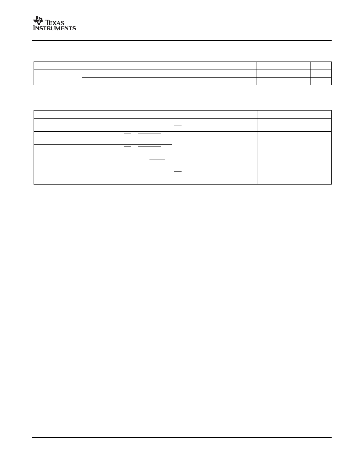
Typical Characteristics
NORMALIZED SENSE THRESHOLD VOLTAGE SUPPLY CURRENT
vs vs
FREE-AIR TEMPERATURE AT V
DD
Figure 2. Figure 3.
INPUT CURRENT MINIMUM PULSE DURATION AT SENSE
vs vs
INPUT VOLTAGE AT MR THRESHOLD OVERDRIVE
SUPPLY VOLTAGE
8
Figure 4. Figure 5.
Submit Documentation Feedback

www.ti.com
1
0.5
0
0 −0.5 −1 −1.5 −2 −2.5 −3
− High-Level Output Voltage − V
1.5
2
2.5
−3.5 −4 −5 −6−4.5 −5.5
IOH − High-Level Output Current − mA
V
OH
85°C
−40°C
VDD = 2V
MR = Open
− High-Level Output Voltage − V
IOH − High-Level Output Current − mA
V
OH
3.5
3
2
0
0 −5 −10 −15 −20 −25 −30
4.5
6
6.5
−35 −40 −45 −50
85°C
−40°C
5.5
5
4
2.5
1.5
1
0.5
VDD = 6V
MR = Open
85°C
−40°C
VDD = 2V
MR = Open
1
0.5
0
0 0.5 1 1.5 2 3 3.5
− Low-Level Output Voltage − V
1.5
2
2.5
4 4.5 5.5 62.5 5
IOL − Low-Level Output Current − mA
V
OL
3.5
3
1.5
0
0 5 10 15 20 30 35
4.5
5.5
6.5
40 50 55 60
85°C
−40°C
VDD = 6V
MR = Open
− Low-Level Output Voltage − V
IOL − Low-Level Output Current − mA
V
OL
6
5
4
2.5
2
1
0.5
25 45
Typical Characteristics (continued)
TPS3307-18 , TPS3307-25 , TPS3307-33
SLVS199C – DECEMBER 1998 – REVISED DECEMBER 2006
HIGH-LEVEL OUTPUT VOLTAGE HIGH-LEVEL OUTPUT VOLTAGE
HIGH-LEVEL OUTPUT CURRENT HIGH-LEVEL OUTPUT CURRENT
LOW-LEVEL OUTPUT VOLTAGE LOW-LEVEL OUTPUT VOLTAGE
LOW-LEVEL OUTPUT CURRENT LOW-LEVEL OUTPUT CURRENT
vs vs
Figure 6. Figure 7.
vs vs
Figure 8. Figure 9.
Submit Documentation Feedback
9

PACKAGE OPTION ADDENDUM
www.ti.com
PACKAGING INFORMATION
Orderable Device Status
TPS3307-18D ACTIVE SOIC D 8 75 RoHS & Green NIPDAU Level-1-260C-UNLIM -40 to 85 30718
TPS3307-18DG4 ACTIVE SOIC D 8 75 RoHS & Green NIPDAU Level-1-260C-UNLIM -40 to 85 30718
TPS3307-18DGN ACTIVE HVSSOP DGN 8 80 RoHS & Green NIPDAU Level-1-260C-UNLIM -40 to 85 AAP
TPS3307-18DGNG4 ACTIVE HVSSOP DGN 8 80 RoHS & Green NIPDAU Level-1-260C-UNLIM -40 to 85 AAP
TPS3307-18DGNR ACTIVE HVSSOP DGN 8 2500 RoHS & Green NIPDAU Level-1-260C-UNLIM -40 to 85 AAP
TPS3307-18DGNRG4 ACTIVE HVSSOP DGN 8 2500 RoHS & Green NIPDAU Level-1-260C-UNLIM -40 to 85 AAP
TPS3307-18DR ACTIVE SOIC D 8 2500 RoHS & Green NIPDAU Level-1-260C-UNLIM -40 to 85 30718
TPS3307-18DRG4 ACTIVE SOIC D 8 2500 RoHS & Green NIPDAU Level-1-260C-UNLIM -40 to 85 30718
TPS3307-25D ACTIVE SOIC D 8 75 RoHS & Green NIPDAU Level-1-260C-UNLIM -40 to 85 30725
TPS3307-25DG4 ACTIVE SOIC D 8 75 RoHS & Green NIPDAU Level-1-260C-UNLIM -40 to 85 30725
TPS3307-25DGN ACTIVE HVSSOP DGN 8 80 RoHS & Green NIPDAU Level-1-260C-UNLIM -40 to 85 AAQ
Package Type Package
(1)
Drawing
Pins Package
Qty
Eco Plan
(2)
Lead finish/
Ball material
(6)
MSL Peak Temp
(3)
Op Temp (°C) Device Marking
10-Dec-2020
Samples
(4/5)
TPS3307-25DGNG4 ACTIVE HVSSOP DGN 8 80 RoHS & Green NIPDAU Level-1-260C-UNLIM -40 to 85 AAQ
TPS3307-25DGNR ACTIVE HVSSOP DGN 8 2500 RoHS & Green NIPDAU Level-1-260C-UNLIM -40 to 85 AAQ
TPS3307-25DGNRG4 ACTIVE HVSSOP DGN 8 2500 RoHS & Green NIPDAU Level-1-260C-UNLIM -40 to 85 AAQ
TPS3307-25DR ACTIVE SOIC D 8 2500 RoHS & Green NIPDAU Level-1-260C-UNLIM -40 to 85 30725
TPS3307-25DRG4 ACTIVE SOIC D 8 2500 RoHS & Green NIPDAU Level-1-260C-UNLIM -40 to 85 30725
TPS3307-33D ACTIVE SOIC D 8 75 RoHS & Green NIPDAU Level-1-260C-UNLIM -40 to 85 30733
TPS3307-33DG4 ACTIVE SOIC D 8 75 RoHS & Green NIPDAU Level-1-260C-UNLIM -40 to 85 30733
TPS3307-33DGN ACTIVE HVSSOP DGN 8 80 RoHS & Green NIPDAU Level-1-260C-UNLIM -40 to 85 AAR
TPS3307-33DGNR ACTIVE HVSSOP DGN 8 2500 RoHS & Green NIPDAU Level-1-260C-UNLIM -40 to 85 AAR
Addendum-Page 1

PACKAGE OPTION ADDENDUM
www.ti.com
Orderable Device Status
TPS3307-33DGNRG4 ACTIVE HVSSOP DGN 8 2500 RoHS & Green NIPDAU Level-1-260C-UNLIM -40 to 85 AAR
TPS3307-33DR ACTIVE SOIC D 8 2500 RoHS & Green NIPDAU Level-1-260C-UNLIM -40 to 85 30733
TPS3307-33DRG4 ACTIVE SOIC D 8 2500 RoHS & Green NIPDAU Level-1-260C-UNLIM -40 to 85 30733
(1)
The marketing status values are defined as follows:
ACTIVE: Product device recommended for new designs.
LIFEBUY: TI has announced that the device will be discontinued, and a lifetime-buy period is in effect.
NRND: Not recommended for new designs. Device is in production to support existing customers, but TI does not recommend using this part in a new design.
PREVIEW: Device has been announced but is not in production. Samples may or may not be available.
OBSOLETE: TI has discontinued the production of the device.
Package Type Package
(1)
Drawing
Pins Package
Qty
Eco Plan
(2)
Lead finish/
Ball material
(6)
MSL Peak Temp
(3)
Op Temp (°C) Device Marking
10-Dec-2020
(4/5)
(2)
RoHS: TI defines "RoHS" to mean semiconductor products that are compliant with the current EU RoHS requirements for all 10 RoHS substances, including the requirement that RoHS substance
do not exceed 0.1% by weight in homogeneous materials. Where designed to be soldered at high temperatures, "RoHS" products are suitable for use in specified lead-free processes. TI may
reference these types of products as "Pb-Free".
RoHS Exempt: TI defines "RoHS Exempt" to mean products that contain lead but are compliant with EU RoHS pursuant to a specific EU RoHS exemption.
Green: TI defines "Green" to mean the content of Chlorine (Cl) and Bromine (Br) based flame retardants meet JS709B low halogen requirements of <=1000ppm threshold. Antimony trioxide based
flame retardants must also meet the <=1000ppm threshold requirement.
(3)
MSL, Peak Temp. - The Moisture Sensitivity Level rating according to the JEDEC industry standard classifications, and peak solder temperature.
(4)
There may be additional marking, which relates to the logo, the lot trace code information, or the environmental category on the device.
(5)
Multiple Device Markings will be inside parentheses. Only one Device Marking contained in parentheses and separated by a "~" will appear on a device. If a line is indented then it is a continuation
of the previous line and the two combined represent the entire Device Marking for that device.
(6)
Lead finish/Ball material - Orderable Devices may have multiple material finish options. Finish options are separated by a vertical ruled line. Lead finish/Ball material values may wrap to two
lines if the finish value exceeds the maximum column width.
Important Information and Disclaimer:The information provided on this page represents TI's knowledge and belief as of the date that it is provided. TI bases its knowledge and belief on information
provided by third parties, and makes no representation or warranty as to the accuracy of such information. Efforts are underway to better integrate information from third parties. TI has taken and
continues to take reasonable steps to provide representative and accurate information but may not have conducted destructive testing or chemical analysis on incoming materials and chemicals.
TI and TI suppliers consider certain information to be proprietary, and thus CAS numbers and other limited information may not be available for release.
In no event shall TI's liability arising out of such information exceed the total purchase price of the TI part(s) at issue in this document sold by TI to Customer on an annual basis.
Samples
Addendum-Page 2

PACKAGE OPTION ADDENDUM
www.ti.com
OTHER QUALIFIED VERSIONS OF TPS3307 :
Enhanced Product: TPS3307-EP
•
NOTE: Qualified Version Definitions:
Enhanced Product - Supports Defense, Aerospace and Medical Applications
•
10-Dec-2020
Addendum-Page 3

PACKAGE MATERIALS INFORMATION
www.ti.com 6-Sep-2019
TAPE AND REEL INFORMATION
*All dimensions are nominal
Device Package
Type
TPS3307-18DGNR HVSSOP DGN 8 2500 330.0 12.4 5.3 3.4 1.4 8.0 12.0 Q1
TPS3307-18DR SOIC D 8 2500 330.0 12.4 6.4 5.2 2.1 8.0 12.0 Q1
TPS3307-25DGNR HVSSOP DGN 8 2500 330.0 12.4 5.3 3.4 1.4 8.0 12.0 Q1
TPS3307-25DR SOIC D 8 2500 330.0 12.4 6.4 5.2 2.1 8.0 12.0 Q1
TPS3307-33DGNR HVSSOP DGN 8 2500 330.0 12.4 5.3 3.4 1.4 8.0 12.0 Q1
TPS3307-33DR SOIC D 8 2500 330.0 12.4 6.4 5.2 2.1 8.0 12.0 Q1
Package
Drawing
Pins SPQ Reel
Diameter
(mm)
Reel
Width
W1 (mm)
A0
(mm)B0(mm)K0(mm)P1(mm)W(mm)
Pin1
Quadrant
Pack Materials-Page 1

PACKAGE MATERIALS INFORMATION
www.ti.com 6-Sep-2019
*All dimensions are nominal
Device Package Type Package Drawing Pins SPQ Length (mm) Width (mm) Height (mm)
TPS3307-18DGNR HVSSOP DGN 8 2500 358.0 335.0 35.0
TPS3307-18DR SOIC D 8 2500 350.0 350.0 43.0
TPS3307-25DGNR HVSSOP DGN 8 2500 358.0 335.0 35.0
TPS3307-25DR SOIC D 8 2500 350.0 350.0 43.0
TPS3307-33DGNR HVSSOP DGN 8 2500 358.0 335.0 35.0
TPS3307-33DR SOIC D 8 2500 350.0 350.0 43.0
Pack Materials-Page 2

GENERIC PACKAGE VIEW
PowerPAD VSSOP - 1.1 mm max heightDGN 8
3 x 3, 0.65 mm pitch
This image is a representation of the package family, actual package may vary.
SMALL OUTLINE PACKAGE
Refer to the product data sheet for package details.
www.ti.com
4225482/A

PACKAGE OUTLINE
SCALE 4.000
5.05
A
1
TYP
4.75
PIN 1 INDEX AREA
PowerPAD VSSOP - 1.1 mm max heightDGN0008D
8
TM
6X 0.65
SMALL OUTLINE PACKAGE
C
0.1 C
SEATING
PLANE
3.1
2.9
NOTE 3
1.89
1.63
2X
1.95
4
5
B
4
3.1
2.9
NOTE 4
SEE DETAIL A
EXPOSED THERMAL PAD
5
9
0.23
0.13
8X
0.38
0.25
0.13 C A B
0.25
GAGE PLANE
1.1 MAX
8
NOTES:
1
1.57
1.28
0 -8
PowerPAD is a trademark of Texas Instruments.
0.7
0.4
A 20
DETAIL A
TYPICAL
4225481/A 11/2019
1. All linear dimensions are in millimeters. Any dimensions in parenthesis are for reference only. Dimensioning and tolerancing
per ASME Y14.5M.
2. This drawing is subject to change without notice.
3. This dimension does not include mold flash, protrusions, or gate burrs. Mold flash, protrusions, or gate burrs shall not
exceed 0.15 mm per side.
4. This dimension does not include interlead flash. Interlead flash shall not exceed 0.25 mm per side.
5. Reference JEDEC registration MO-187.
www.ti.com
0.15
0.05

METAL COVERED
BY SOLDER MASK
8X (1.4)
(2)
NOTE 9
(1.57)
SYMM
EXAMPLE BOARD LAYOUT
TM
PowerPAD VSSOP - 1.1 mm max heightDGN0008D
SMALL OUTLINE PACKAGE
SOLDER MASK
DEFINED PAD
(R0.05) TYP
8X (0.45)
6X (0.65)
( 0.2) TYP
SOLDER MASK
OPENING
EXPOSED METAL
1
4
VIA
9
(0.55)
(4.4)
LAND PATTERN EXAMPLE
EXPOSED METAL SHOWN
SCALE: 15X
METAL
METAL UNDER
SOLDER MASK
8
SYMM
(1.22)
5
SEE DETAILS
SOLDER MASK
OPENING
(3)
NOTE 9
(1.89)
EXPOSED METAL
0.05 MAX
ALL AROUND
NON-SOLDER MASK
DEFINED
(PREFERRED)
SOLDER MASK DETAILS
15.000
0.05 MIN
ALL AROUND
SOLDER MASK
DEFINED
4225481/A 11/2019
NOTES: (continued)
6. Publication IPC-7351 may have alternate designs.
7. Solder mask tolerances between and around signal pads can vary based on board fabrication site.
8. Vias are optional depending on application, refer to device data sheet. If any vias are implemented, refer to their locations shown
on this view. It is recommended that vias under paste be filled, plugged or tented.
9. Size of metal pad may vary due to creepage requirement.
www.ti.com

PowerPAD VSSOP - 1.1 mm max heightDGN0008D
(1.57)
BASED ON
0.125 THICK
STENCIL
SYMM
EXAMPLE STENCIL DESIGN
TM
SMALL OUTLINE PACKAGE
8X (0.45)
6X (0.65)
METAL COVERED
BY SOLDER MASK
1
4
8X (1.4)
(4.4)
SOLDER PASTE EXAMPLE
100% PRINTED SOLDER COVERAGE BY AREA
STENCIL
THICKNESS
EXPOSED PAD 9:
SCALE: 15X
SOLDER STENCIL
OPENING
1.76 X 2.110.1
1.57 X 1.89 (SHOWN)0.125
1.43 X 1.730.15
1.33 X 1.600.175
(R0.05) TYP
8
SYMM
5
SEE TABLE FOR
DIFFERENT OPENINGS
FOR OTHER STENCIL
THICKNESSES
(1.89)
BASED ON
0.125 THICK
STENCIL
4225481/A 11/2019
NOTES: (continued)
10. Laser cutting apertures with trapezoidal walls and rounded corners may offer better paste release. IPC-7525 may have alternate
design recommendations.
11. Board assembly site may have different recommendations for stencil design.
www.ti.com

PACKAGE OUTLINE
A
.189-.197
[4.81-5.00]
NOTE 3
.228-.244 TYP
[5.80-6.19]
1
4
B .150-.157
[3.81-3.98]
PIN 1 ID AREA
NOTE 4
SCALE 2.800
6X .050
[1.27]
8
2X
.150
[3.81]
5
8X .012-.020
[0.31-0.51]
.010 [0.25] C A B
SOIC - 1.75 mm max heightD0008A
SMALL OUTLINE INTEGRATED CIRCUIT
C
SEATING PLANE
.004 [0.1] C
4X (0 -15 )
.069 MAX
[1.75]
.005-.010 TYP
[0.13-0.25]
4X (0 -15 )
SEE DETAIL A
.010
[0.25]
0 - 8
.016-.050
[0.41-1.27]
(.041)
[1.04]
DETAIL A
TYPICAL
.004-.010
[0.11-0.25]
4214825/C 02/2019
NOTES:
1. Linear dimensions are in inches [millimeters]. Dimensions in parenthesis are for reference only. Controlling dimensions are in inches.
Dimensioning and tolerancing per ASME Y14.5M.
2. This drawing is subject to change without notice.
3. This dimension does not include mold flash, protrusions, or gate burrs. Mold flash, protrusions, or gate burrs shall not
exceed .006 [0.15] per side.
4. This dimension does not include interlead flash.
5. Reference JEDEC registration MS-012, variation AA.
www.ti.com

8X (.061 )
8X (.024)
6X (.050 )
[1.27]
[0.6]
[1.55]
SYMM
1
4
(.213)
[5.4]
LAND PATTERN EXAMPLE
EXPOSED METAL SHOWN
SCALE:8X
EXAMPLE BOARD LAYOUT
SOIC - 1.75 mm max heightD0008A
SMALL OUTLINE INTEGRATED CIRCUIT
SEE
DETAILS
8
SYMM
(R.002 ) TYP
5
[0.05]
EXPOSED
METAL
METAL
NON SOLDER MASK
SOLDER MASK
OPENING
.0028 MAX
[0.07]
ALL AROUND
DEFINED
SOLDER MASK
OPENING
EXPOSED
METAL
.0028 MIN
[0.07]
ALL AROUND
SOLDER MASK
DEFINED
SOLDER MASK DETAILS
NOTES: (continued)
6. Publication IPC-7351 may have alternate designs.
7. Solder mask tolerances between and around signal pads can vary based on board fabrication site.
METAL UNDER
SOLDER MASK
4214825/C 02/2019
www.ti.com

8X (.061 )
8X (.024)
6X (.050 )
[1.27]
[0.6]
[1.55]
EXAMPLE STENCIL DESIGN
SOIC - 1.75 mm max heightD0008A
SMALL OUTLINE INTEGRATED CIRCUIT
SYMM
1
8
SYMM
(R.002 ) TYP
4
(.213)
[5.4]
5
[0.05]
BASED ON .005 INCH [0.125 MM] THICK STENCIL
NOTES: (continued)
8. Laser cutting apertures with trapezoidal walls and rounded corners may offer better paste release. IPC-7525 may have alternate
design recommendations.
9. Board assembly site may have different recommendations for stencil design.
SCALE:8X
4214825/C 02/2019
SOLDER PASTE EXAMPLE
www.ti.com

IMPORTANT NOTICE AND DISCLAIMER
TI PROVIDES TECHNICAL AND RELIABILITY DATA (INCLUDING DATASHEETS), DESIGN RESOURCES (INCLUDING REFERENCE
DESIGNS), APPLICATION OR OTHER DESIGN ADVICE, WEB TOOLS, SAFETY INFORMATION, AND OTHER RESOURCES “AS IS”
AND WITH ALL FAULTS, AND DISCLAIMS ALL WARRANTIES, EXPRESS AND IMPLIED, INCLUDING WITHOUT LIMITATION ANY
IMPLIED WARRANTIES OF MERCHANTABILITY, FITNESS FOR A PARTICULAR PURPOSE OR NON-INFRINGEMENT OF THIRD
PARTY INTELLECTUAL PROPERTY RIGHTS.
These resources are intended for skilled developers designing with TI products. You are solely responsible for (1) selecting the appropriate
TI products for your application, (2) designing, validating and testing your application, and (3) ensuring your application meets applicable
standards, and any other safety, security, or other requirements. These resources are subject to change without notice. TI grants you
permission to use these resources only for development of an application that uses the TI products described in the resource. Other
reproduction and display of these resources is prohibited. No license is granted to any other TI intellectual property right or to any third
party intellectual property right. TI disclaims responsibility for, and you will fully indemnify TI and its representatives against, any claims,
damages, costs, losses, and liabilities arising out of your use of these resources.
TI’s products are provided subject to TI’s Terms of Sale (www.ti.com/legal/termsofsale.html) or other applicable terms available either on
ti.com or provided in conjunction with such TI products. TI’s provision of these resources does not expand or otherwise alter TI’s applicable
warranties or warranty disclaimers for TI products.
Mailing Address: Texas Instruments, Post Office Box 655303, Dallas, Texas 75265
Copyright © 2020, Texas Instruments Incorporated
 Loading...