

Datasheet TPS2816DBVR, TPS2816DBV, TPS2829DBVR, TPS2829DBV, TPS2828DBVT Datasheet (Texas Instruments)
...Page 1
TPS2816, TPS2817, TPS2818, TPS2819, TPS2828, TPS2829
SINGLE-CHANNEL HIGH-SPEED MOSFET DRIVER
SLVS160A – FEBRUARY 1997 – REVISED NOVEMBER 1997
1
POST OFFICE BOX 655303 • DALLAS, TEXAS 75265
D
Low-Cost Single-Channel High-Speed
MOSFET Driver
D
ICC...15-µA Max (TPS2828, TPS2829)
D
25-ns Max Rise/Fall Times and 40-ns Max
Propagation Delay...1-nF Load
D
2-A Peak Output Current
D
4-V to 14-V Driver Supply Voltage Range;
Internal Regulator Extends Range to 40 V
(TPS2816, TPS2817, TPS2818, TPS2819)
D
5-pin SOT-23 Package
D
–40°C to 125°C Ambient-Temperature
Operating Range
D
Highly Resistant to Latch-ups
description
The TPS28xx single-channel high-speed MOSFET drivers are capable of delivering peak
currents of up to 2 A into highly capacitive loads.
High switching speeds (t
r
and tf = 14 ns typ) are
obtained with the use of BiCMOS outputs. Typical
threshold switching voltages are 2/3 and 1/3 of
V
CC
. The design inherently minimizes shoot-
through current.
A regulator is provided on TPS2816 through TPS2819 devices to allow operation with supply inputs between
14 V and 40 V. The regulator output can be used to power other circuits, provided power dissipation does not
exceed package limitations. If the regulator is not required, V
DD
(the regulator input) should be connected to
V
CC
. The TPS2816 and TPS2817 input circuits include an active pullup circuit to eliminate the need for an
external resistor when using open-collector PWM controllers. The TPS2818 and TPS2819 are identical to the
TPS2816 and TPS2817, except that the active pullup circuit is omitted. The TPS2828 and TPS2829 are
identical to the TPS2818 and TPS2819, except that the internal voltage regulator is omitted, allowing quiescent
current to drop to less than 15 µA when the inputs are high or low.
The TPS28xx series devices are available in 5-pin SOT-23 (DBV) packages and operate over an ambient
temperature range of –40_C to 125_C.
AVAILABLE OPTIONS
PACKAGED DEVICES
CHIP FORM
T
A
FUNCTION
SOT-23–5 (DBV)
(Y)
Inverting driver with active pullup input TPS2816DBV TPS2816Y
Noninverting driver with active pullup input TPS2817DBV TPS2817Y
°
°
Inverting driver TPS2818DBV TPS2818Y
–
40°C to 125°C
Noninverting driver TPS2819DBV TPS2819Y
Inverting driver, no regulator TPS2828DBV TPS2828Y
Noninverting driver, no regulator TPS2829DBV TPS2829Y
The DBV package is available taped and reeled only.
Copyright 1997, Texas Instruments Incorporated
PRODUCTION DATA information is current as of publication date.
Products conform to specifications per the terms of Texas Instruments
standard warranty. Production processing does not necessarily include
testing of all parameters.
Please be aware that an important notice concerning availability, standard warranty, and use in critical applications of
Texas Instruments semiconductor products and disclaimers thereto appears at the end of this data sheet.
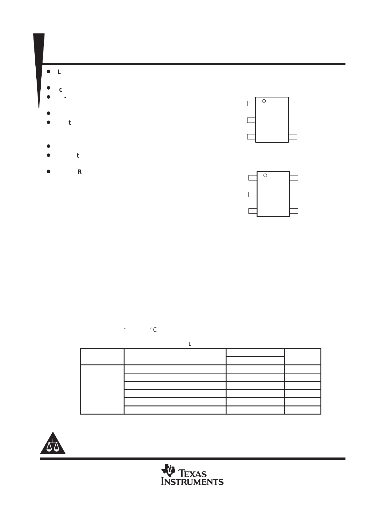
3
2
1
4
5
IN
V
CC
V
DD
OUT
TPS2816, TPS2817
TPS2818, TPS2819
DBV PACKAGE
(TOP VIEW)
GND
3
2
1
4
5
IN
V
CC
NC
OUT
DBV PACKAGE
(TOP VIEW)
GND
TPS2828, TPS2829
NC – No internal connection
Page 2
TPS2816, TPS2817, TPS2818, TPS2819, TPS2828, TPS2829
SINGLE-CHANNEL HIGH-SPEED MOSFET DRIVER
SLVS160A – FEBRUARY 1997 – REVISED NOVEMBER 1997
2
POST OFFICE BOX 655303 • DALLAS, TEXAS 75265
functional block diagram
VREG
V
DD
IN
GND
V
CC
OUT
TPS2816, TPS2818
Active Pullup
(TPS2816 Only)
VREG
V
DD
IN
GND
V
CC
OUT
TPS2817, TPS2819
Active Pullup
(TPS2817 Only)
IN
GND
OUT
TPS2828
IN
GND
OUT
TPS2829
V
CC
V
CC
INPUT STAGE DIAGRAM
To Drive
Stage
IN
V
CC
OUTPUT STAGE DIAGRAM
V
CC
OUT
Predrive
Page 3
TPS2816, TPS2817, TPS2818, TPS2819, TPS2828, TPS2829
SINGLE-CHANNEL HIGH-SPEED MOSFET DRIVER
SLVS160A – FEBRUARY 1997 – REVISED NOVEMBER 1997
3
POST OFFICE BOX 655303 • DALLAS, TEXAS 75265
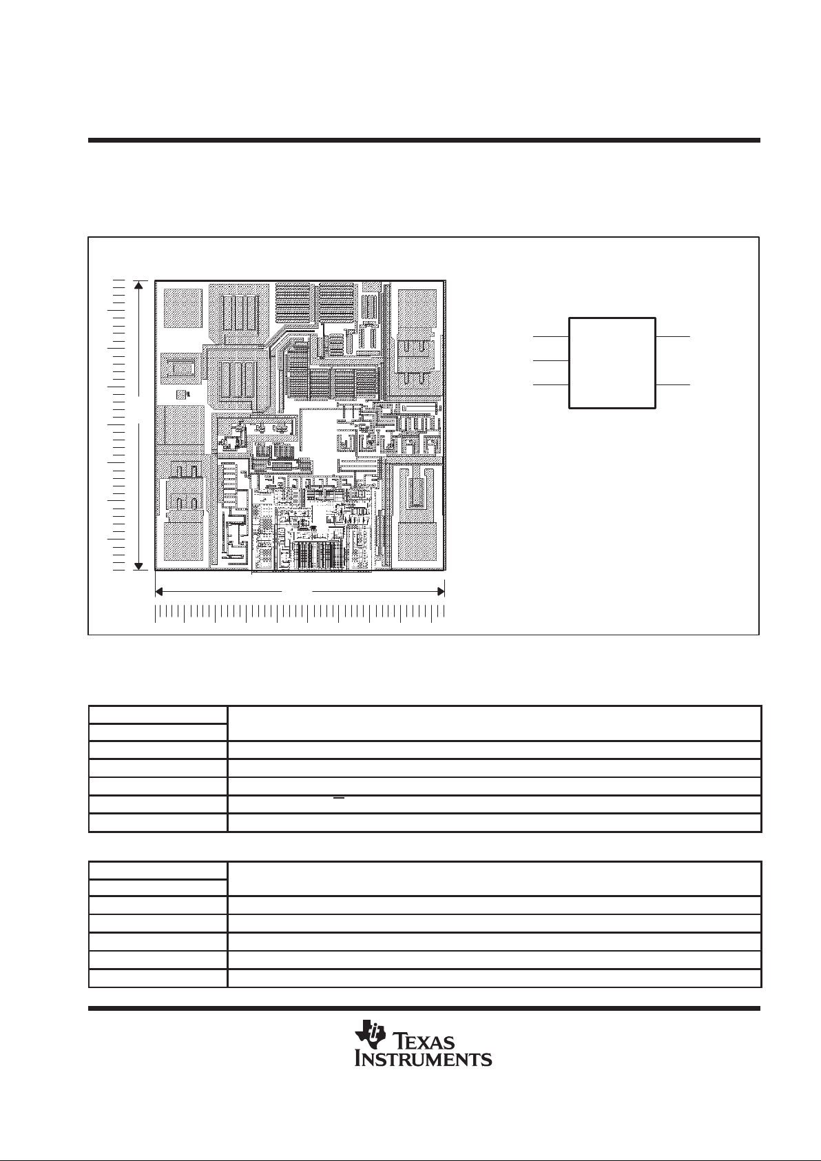
TPS28xxY chip information
This chip, when properly assembled, displays characteristics similar to those of the TPS28xx. Thermal
compression or ultrasonic bonding may be used on the doped aluminum bonding pads. The chip may be
mounted with conductive epoxy or a gold-silicon preform.
39
39
TPS2816Y
(4)
(2)
(3)
(5)
(1)
OUT
GND
IN
V
CC
V
DD
†
BONDING PAD ASSIGNMENTS
CHIP THICKNESS: 15 TYPICAL
BONDING PADS: 4 × 4 MINIMUM
TJ max = 150°C
TOLERANCES ARE ±10%.
ALL DIMENSIONS ARE IN MILS.
(4)
(2)
(3)
(1)
(5)
†
TPS2816 through TPS2819 only
Terminal Functions
TPS2816, TPS2818, TPS2828 (inverting driver)
TERMINAL
NAME NO.
DESCRIPTION
V
DD
1 Regulator supply voltage input. (Not connected on TPS2828)
GND 2 Ground
IN 3 Driver input.
OUT 4 Driver output, OUT = IN
V
CC
5 Driver supply voltage/regulator output voltage
TPS2817, TPS2819, TPS2829 (noninverting driver)
TERMINAL
NAME NO.
DESCRIPTION
V
DD
1 Regulator supply voltage input. (Not connected on TPS2829)
GND 2 Ground
IN 3 Driver input.
OUT 4 Driver output, OUT= IN
V
CC
5 Driver supply voltage/regulator output voltage
Page 4
TPS2816, TPS2817, TPS2818, TPS2819, TPS2828, TPS2829
SINGLE-CHANNEL HIGH-SPEED MOSFET DRIVER
SLVS160A – FEBRUARY 1997 – REVISED NOVEMBER 1997
4
POST OFFICE BOX 655303 • DALLAS, TEXAS 75265
DISSIPATION RATING TABLE
PACKAGE
TA ≤ 25°C
POWER RATING
DERATING FACTOR
ABOVE TA = 25°C
TA = 70°C
POWER RATING
TA = 80°C
POWER RATING
DBV 437 mW 3.5 mW/°C 280 mW 227 mW
These dissipation ratings are based upon EIA specification JESD51-3, ”Low Effective Thermal
Conductivity T est Board for Leaded Surface Mount Packages,” in tests conducted in a zero-airflow , wind
tunnel environment.
absolute maximum ratings over operating temperature range (unless otherwise noted)
†
Regulator supply voltage range, V
DD
–0.3 V to 42 V. . . . . . . . . . . . . . . . . . . . . . . . . . . . . . . . . . . . . . . . . . . . . . . .
Supply voltage range, V
CC
–0.3 V to 15 V. . . . . . . . . . . . . . . . . . . . . . . . . . . . . . . . . . . . . . . . . . . . . . . . . . . . . . . . .
Input voltage range, IN –0.3 V to 15 V. . . . . . . . . . . . . . . . . . . . . . . . . . . . . . . . . . . . . . . . . . . . . . . . . . . . . . . . . . . .
Continuous regulator output current, V
CC
25 mA. . . . . . . . . . . . . . . . . . . . . . . . . . . . . . . . . . . . . . . . . . . . . . . . . . .
Continuous output current, OUT ±100 mA. . . . . . . . . . . . . . . . . . . . . . . . . . . . . . . . . . . . . . . . . . . . . . . . . . . . . . . .
Continuous total power dissipation See Dissipation Rating Table. . . . . . . . . . . . . . . . . . . . . . . . . . . . . . . . . . . . . .
Operating ambient temperature range, T
A
–40°C to 125°C. . . . . . . . . . . . . . . . . . . . . . . . . . . . . . . . . . .
Storage temperature range, T
stg
–65°C to 150°C. . . . . . . . . . . . . . . . . . . . . . . . . . . . . . . . . . . . . . . . . .
Lead temperature 1,6 mm (1/16inch) from case for 10 seconds 260°C. . . . . . . . . . . . . . . . . . . . . . . . . . . . . . . . .
†
Stresses beyond those listed under “absolute maximum ratings” may cause permanent damage to the device. These are stress ratings only, and
functional operation of the device at these or any other conditions beyond those indicated under “recommended operating conditions” is not
implied. Exposure to absolute-maximum-rated conditions for extended periods may affect device reliability.
NOTE 1: All voltages are with respect to device GND terminal.
recommended operating conditions
MIN MAX UNIT
Regulator input voltage range, VDD, TPS2816 through TPS2819 8 40 V
Supply voltage, V
CC
4 14 V
Input voltage, IN –0.3 V
CC
V
Continuous regulator output current, I
CC
0 20 mA
Operating ambient temperature range, T
A
–40 125
_
C
Page 5
TPS2816, TPS2817, TPS2818, TPS2819, TPS2828, TPS2829
SINGLE-CHANNEL HIGH-SPEED MOSFET DRIVER
SLVS160A – FEBRUARY 1997 – REVISED NOVEMBER 1997
5
POST OFFICE BOX 655303 • DALLAS, TEXAS 75265
TPS28xx electrical characteristics over recommended operating ambient temperature range,
V
CC
= 10 V, VDD tied to VCC, CL = 1 nF (unless otherwise specified)
Inputs
PARAMETER TEST CONDITIONS MIN TYP†MAX UNIT
VCC = 5 V 3.3 4
Positive-going input threshold voltage
VCC = 10 V
6.6 7
V
VCC = 14 V 9.3 10
VCC = 5 V 1 1.7
Negative-going input threshold voltage
VCC = 10 V
2 3.3
V
VCC = 14 V 2.5 4.6
Input voltage hysteresis 1.3 V
Input current, TPS2818/19/28/29 Input = 0 V or V
CC
0.2 µA
p
Input = 0 V 650
Input current, TPS2816/17
Input = V
CC
15
µ
A
Input capacitance 5 10 pF
†
Typicals are for TA = 25°C unless otherwise noted.
outputs
PARAMETER TEST CONDITIONS MIN TYP†MAX UNIT
IO = –1 mA 9.75 9.9
High-l
evel output voltage
IO = –100 mA
8 9.1
V
p
IO = 1 mA 0.18 0.25
Low-level output voltage
IO = 100 mA 1 2
V
†
Typicals are for TA = 25°C unless otherwise noted.
regulator, TPS2816 through TPS2819
PARAMETER TEST CONDITIONS MIN TYP†MAX UNIT
p
14 ≤ VDD ≤ 40 V, 10 11.5 13
Output voltage
DD
0 ≤ IO ≤ 20 mA
V
p
p
IO = 10 mA, 8 10
Out ut voltage in dro out
VDD = 10 V
V
†
Typicals are for TA = 25°C unless otherwise noted.
supply current
PARAMETER TEST CONDITIONS MIN TYP†MAX UNIT
TPS2816,
IN = high = 10 V 150 250
,
TPS2817
IN = low = 0 V 650 1000
pp
TPS2818,
Su ly current into V
CC
,
TPS2819
IN = high or low,
25
50
µA
TPS2828,
TPS2829
g
High = 10 V, Low = 0 V
0.1 15
TPS2816, V
= 20 V,
pp
,
TPS2817
DD
,
IN = high = 10 V or low = 0 V
650
1000
Supply current into V
DD
TPS2818,
V
= 20 V,
µ
A
,
TPS2819
DD
,
IN = high = 10 V or low = 0 V
50
150
†
Typicals are for TA = 25°C unless otherwise noted.
Page 6
TPS2816, TPS2817, TPS2818, TPS2819, TPS2828, TPS2829
SINGLE-CHANNEL HIGH-SPEED MOSFET DRIVER
SLVS160A – FEBRUARY 1997 – REVISED NOVEMBER 1997
6
POST OFFICE BOX 655303 • DALLAS, TEXAS 75265
TPS28xxY electrical characteristics at TA = 25_C, V
CC
= 10 V, VDD tied to VCC, CL = 1 nF
(unless otherwise specified)
Inputs
PARAMETER TEST CONDITIONS MIN TYP MAX UNIT
VCC = 5 V 3.3
Positive-going input threshold voltage
VCC = 10 V
6.6
V
VCC = 14 V 9.3
VCC = 5 V 1.7
Negative-going input threshold voltage
VCC = 10 V
3.3
V
VCC = 14 V 4.6
Input voltage hysteresis 1.3 V
Input current, TPS2818/19/28/29 Input = 0 V or V
CC
0.2 µA
p
Input = 0 V 650
Input current, TPS2816/17
Input = V
CC
15
µ
A
Input resistance 1000 MΩ
Input capacitance 5 pF
outputs
PARAMETER TEST CONDITIONS MIN TYP MAX UNIT
IO = –1 mA 9.9
High-l
evel output voltage
IO = –100 mA 9.1
V
p
IO = 1 mA 0.18
Low-level output voltage
IO = 100 mA 1
V
regulator, TPS2816 through TPS2819
PARAMETER TEST CONDITIONS MIN TYP MAX UNIT
Output voltage 14 ≤ VDD ≤ 40 V,
0 ≤ IO ≤ 20 mA
11.5 V
Output voltage in dropout IO = 10 mA,
VDD = 10 V
9 V
supply current
PARAMETER TEST CONDITIONS MIN TYP MAX UNIT
TPS2816,
IN = high = 10 V 150
,
TPS2817
IN = low = 0 V 650
pp
TPS2818,
Su ly current into V
CC
,
TPS2819
IN = high or low,
25
µA
TPS2828,
TPS2829
g
High = 10 V, Low = 0 V
0.1
TPS2816, V
= 20 V,
pp
,
TPS2817
DD
,
IN = high = 10 V or low = 0 V
650
Supply current into V
DD
TPS2818,
V
= 20 V,
µ
A
,
TPS2819
DD
,
IN = high = 10 V or low = 0 V
50
Page 7

TPS2816, TPS2817, TPS2818, TPS2819, TPS2828, TPS2829
SINGLE-CHANNEL HIGH-SPEED MOSFET DRIVER
SLVS160A – FEBRUARY 1997 – REVISED NOVEMBER 1997
7
POST OFFICE BOX 655303 • DALLAS, TEXAS 75265
switching characteristics for all devices over recommended operating ambient temperature range,
V
CC
= 10 V, VDD tied to VCC, CL = 1 nF (unless otherwise specified)
PARAMETER TEST CONDITIONS MIN TYP MAX UNIT
VCC = 14 V 25
t
r
Rise time
VCC = 10 V 14 30
ns
VCC = 5 V 35
VCC = 14 V 25
t
f
Fall time
VCC = 10 V
14 30
ns
VCC = 5 V 35
VCC = 14 V 40
t
PHL
Propagation delay time, high-to-low-level output
VCC = 10 V
24 45
ns
VCC = 5 V 50
VCC = 14 V 40
t
PLH
Propagation delay time, low-to-high-level output
VCC = 10 V
24 45
ns
VCC = 5 V 50
PARAMETER MEASUREMENT INFORMATION
50%
90%
IN
OUT
50% 50%
90%
10%
50%
10%
t
PLH
t
r
t
f
t
PHL
0 V
0 V
Figure 1. Typical Timing Diagram (TPS2816)
Page 8

TPS2816, TPS2817, TPS2818, TPS2819, TPS2828, TPS2829
SINGLE-CHANNEL HIGH-SPEED MOSFET DRIVER
SLVS160A – FEBRUARY 1997 – REVISED NOVEMBER 1997
8
POST OFFICE BOX 655303 • DALLAS, TEXAS 75265
PARAMETER MEASUREMENT INFORMATION
Regulator
50 Ω
0.1 µF
4.7 µF
+
10 V
1 nF
1
2
3
5
4
Input
Output
TPS2816
Figure 2. Switching Time Test Setup
0–10 Vdc
OUT
0.1 µF 4.7 µF
10 V
Current
Loop
+
V
CC
TPS2816
Figure 3. Shoot-Through Current Test Setup
Page 9

TPS2816, TPS2817, TPS2818, TPS2819, TPS2828, TPS2829
SINGLE-CHANNEL HIGH-SPEED MOSFET DRIVER
SLVS160A – FEBRUARY 1997 – REVISED NOVEMBER 1997
9
POST OFFICE BOX 655303 • DALLAS, TEXAS 75265
TYPICAL CHARACTERISTICS
Table of Graphs
FIGURE
Rise time vs Supply voltage 4
Fall time vs Supply voltage 5
Propagation time (L>H) vs Supply voltage 6
Propagation Time (H>L) vs Supply voltage 7
Rise time vs Ambient temperature 8
Fall time vs Ambient temperature 9
Propagation time (L>H) vs Supply voltage 10
Propagation time (H>L) vs Ambient temperature 11
Supply current (VCC) vs Supply voltage 12
Supply current (VCC) vs Load capacitance 13
Supply current (VCC) vs Ambient temperature 14
Input threshold voltage vs Supply voltage 15
Regulator output voltage vs Regulator supply voltage 16
Regulator quiescent current vs Regulator supply voltage 17
Shoot-through current vs Input voltage (L>H) 18
Shoot-through current vs Input voltage (H>L) 19
Page 10

TPS2816, TPS2817, TPS2818, TPS2819, TPS2828, TPS2829
SINGLE-CHANNEL HIGH-SPEED MOSFET DRIVER
SLVS160A – FEBRUARY 1997 – REVISED NOVEMBER 1997
10
POST OFFICE BOX 655303 • DALLAS, TEXAS 75265
TYPICAL CHARACTERISTICS
Figure 4
20
10
5
0
46810
25
30
35
12 14
– Rise Time – ns
RISE TIME
vs
SUPPLY VOLTAGE
t
r
VCC – Supply Voltage – V
15
TA = 25°C
CL = 2200 pF
CL = 1000 pF
CL = 0
Figure 5
15
10
5
0
46810
20
25
30
12 14
– Fall Time – ns
FALL TIME
vs
SUPPLY VOLTAGE
t
f
VCC – Supply Voltage – V
TA = 25°C
CL = 2200 pF
CL = 1000 pF
CL = 0
Figure 6
20
15
5
0
46810
25
35
40
12 14
Propagation Delay Time,
PROPAGATION DELAY TIME,
LOW-TO-HIGH-LEVEL OUTPUT
vs
SUPPLY VOLTAGE
VCC – Supply Voltage – V
t –
PLH
Low-To-High-Level Output – ns
30
10
TA = 25°C
CL = 2200 pF
CL = 1000 pF
CL = 0
Figure 7
20
15
5
0
46810
25
35
40
12 14
TA = 25°C
CL = 2200 pF
CL = 1000 pF
CL = 0
Propagation Delay Time,
PROPAGATION DELAY TIME,
HIGH-TO-LOW-LEVEL OUTPUT
vs
SUPPLY VOLTAGE
VCC – Supply Voltage – V
t –
PHL
High-To-Low-Level Output – ns
30
10
Page 11

TPS2816, TPS2817, TPS2818, TPS2819, TPS2828, TPS2829
SINGLE-CHANNEL HIGH-SPEED MOSFET DRIVER
SLVS160A – FEBRUARY 1997 – REVISED NOVEMBER 1997
11
POST OFFICE BOX 655303 • DALLAS, TEXAS 75265
TYPICAL CHARACTERISTICS
Figure 8
16
15
14
13
–50 –25 0 25 50
– Rise Time – ns
17
18
RISE TIME
vs
AMBIENT TEMPERATURE
19
75 100 125
Ambient Temperature – °C
VCC = 10 V
Load = 1000 pF
f = 100 kHz
t
r
Figure 9
15
13
12
10
–50 –25 0 25 50
17
18
20
75 100 125
– Fall Time – ns
FALL TIME
vs
AMBIENT TEMPERATURE
Ambient Temperature – °C
VCC = 10 V
Load = 1000 pF
f = 100 kHz
t
f
19
16
14
11
Figure 10
16
15
14
13
–50 –25 0 25 50
17
18
19
75 100 125
VCC = 10 V
Load = 1000 pF
f = 100 kHz
Propagation Delay Time,
PROPAGATION DELAY TIME,
LOW-TO-HIGH-LEVEL OUTPUT
vs
SUPPLY VOLTAGE
t –
PLH
Low-To-High-Level Output – ns
TA – Ambient Temperature – °C
Figure 11
Propagation Delay Time,
PROPAGATION DELAY TIME,
HIGH-TO-LOW-LEVEL OUTPUT
vs
AMBIENT TEMPERATURE
t –
PHL
High-To-Low-Level Output – ns
15
14
12
10
–50 –25 0 25 50
17
19
20
75 100 125
VCC = 10 V
Load = 1000 pF
f = 100 kHz
TA – Ambient Temperature – °C
18
16
13
11
Page 12

TPS2816, TPS2817, TPS2818, TPS2819, TPS2828, TPS2829
SINGLE-CHANNEL HIGH-SPEED MOSFET DRIVER
SLVS160A – FEBRUARY 1997 – REVISED NOVEMBER 1997
12
POST OFFICE BOX 655303 • DALLAS, TEXAS 75265
TYPICAL CHARACTERISTICS
Figure 12
VCC – Supply Voltage – V
Load = 1000 pF
Duty Cycle = 50%
f = 1 MHz
f = 500 kHz
f = 100 kHz
f = 40 kHz
8
6
2
0
46810
– Supply Current – mA
12
14
SUPPLY CURRENT
vs
SUPPLY VOLTAGE
16
12 14
I
CC
10
4
Figure 13
2
1.5
1
0
0 1000
3
3.5
SUPPLY CURRENT
vs
LOAD CAPACITANCE
4
2000
2.5
0.5
– Supply Current – mA
I
CC
CL – Load Capacitance – pF
VCC = 10 V
f = 100 kHz
Duty Cycle = 50%
Figure 14
2
1.5
1
–50 –25 0 25 50
2.5
3
75 100 125
VCC = 10 V
Load = 1000 pF
f = 100 kHz
Duty Cycle = 50%
SUPPLY CURRENT
vs
AMBIENT TEMPERATURE
– Supply Current – mAI
CC
TA – Ambient Temperature – °C
Figure 15
4
3
2
0
46 810
– Input Threshold Voltage–V
7
8
INPUT THRESHOLD VOLTAGE
vs
SUPPLY VOLTAGE
9
12 14
VCC – Supply Voltage – V
5
6
1
Positive Going
Negative Going
V
IT
Page 13
TPS2816, TPS2817, TPS2818, TPS2819, TPS2828, TPS2829
SINGLE-CHANNEL HIGH-SPEED MOSFET DRIVER
SLVS160A – FEBRUARY 1997 – REVISED NOVEMBER 1997
13
POST OFFICE BOX 655303 • DALLAS, TEXAS 75265
TYPICAL CHARACTERISTICS
Figure 16
8
7
5
4 8 12 16 20 24
Regulator Output Voltage – V
10
11
REGULATOR OUTPUT VOLTAGE
vs
REGULATOR SUPPLY VOLTAGE
12
28 32 36 40
9
6
4
Load = 10 kΩ
VDD – Regulator Supply Voltage – V
Figure 17
645
640
630
620
4 8 12 16 20 24
Regulator Quiescent Current –
655
665
REGULATOR QUIESCENT CURRENT
vs
REGULATOR SUPPLY VOLTAGE
670
28 32 36 40
660
650
635
625
TPS2816,17 only
No Load
Aµ
VDD – Regulator Supply Voltage – V
Figure 18
VCC = 10 V
No Load
TA = 25°C
4
3
2
0
0246
Shoot-Through Current – mA
5
6
SHOOT-THROUGH CURRENT
vs
INPUT VOLTAGE LOW-TO-HIGH
7
810
1
V
I
– Input Voltage – V
Figure 19
4
3
2
0
0246
5
6
7
810
Shoot-Through Current – mA
SHOOT-THROUGH CURRENT
vs
INPUT VOLTAGE HIGH-TO-LOW
VI – Input Voltage – V
1
VCC = 10 V
No Load
TA = 25°C
Page 14

TPS2816, TPS2817, TPS2818, TPS2819, TPS2828, TPS2829
SINGLE-CHANNEL HIGH-SPEED MOSFET DRIVER
SLVS160A – FEBRUARY 1997 – REVISED NOVEMBER 1997
14
POST OFFICE BOX 655303 • DALLAS, TEXAS 75265
APPLICATION INFORMATION
MOSFET s are voltage-driven devices that require very little steady-state drive current. However , the large input
capacitance (200 pF to 3000 pF or greater) of these devices requires large current surges to reduce the turn-on
and turn-off times. The TPS2816 series of high-speed drivers can supply up to 2 A to a MOSFET, greatly
reducing the switching times. The fast rise times and fall times and short propagation delays allow for operation
in today’s high-frequency switching converters.
In addition, MOSFETs have a limited gate-bias voltage range, usually less than 20 V. The TPS2816 series of
drivers extends this operating range by incorporating an on-board series regulator with an input range up to 40 V.
This regulator can be used to power the drivers, the PWM chip, and other circuitry, providing the power
dissipation rating is not exceeded.
When using these devices, care should be exercised in the proper placement of the driver, the switching
MOSFET, and the bypass capacitor. Because of the large input capacitance of the MOSFET, the driver should
be placed close to the gate to eliminate the possibility of oscillations caused by trace inductance ringing with
the gate capacitance of the MOSFET. When the driver output path is longer than approximately 2 inches, a
resistor in the range of 10 Ω should be placed in series with the gate drive as close as possible to the MOSFET .
A ceramic bypass capacitor is also recommended to provide a source for the high-speed current transients that
the MOSFET requires. This capacitor should be placed between V
CC
and GND of the driver (see Figures 20
and 21).
Regulator
0.1 µF
1
2
3
5
4
Input
TPS2816
V
CC
Load
Figure 20. VCC < 14 V
Regulator
4.7 µF
1
2
3
5
4
Input
TPS2816
V
DD
Load
0.1 µF
+
Figure 21. VCC > 14 V
Page 15

TPS2816, TPS2817, TPS2818, TPS2819, TPS2828, TPS2829
SINGLE-CHANNEL HIGH-SPEED MOSFET DRIVER
SLVS160A – FEBRUARY 1997 – REVISED NOVEMBER 1997
15
POST OFFICE BOX 655303 • DALLAS, TEXAS 75265
APPLICATION INFORMATION
The on-board series regulator supplies approximately 20 mA of current at 1 1.5 V, some of which can be used
for external circuitry, providing the power dissipation rating for the driver is not exceeded. When using the
on-board series regulator, an electrolytic output capacitor of 4.7 µF or larger is recommended. Although not
required, a 0.1-µF ceramic capacitor on the input of the regulator can help suppress transient currents (see
Figure 22). When not used, the regulator should be connected to V
CC
. Grounding VDD will result in destruction
of the regulator.
Regulator
1
2
3
5
4
34 VDC
TPS2816
0.1 µF
PWM
Controller
0.1 µF
4.7 µF
V
CC
Out
GND
0.1 µF
10 µF
V
O
+
Figure 22. Boost Application
The TPS2816 and TPS2818 drivers include active pullup circuits on the inputs to eliminate the need for external
pullup resistors when using controllers with open-collector outputs (such as the TL5001). The TPS2817 and
TPS2819 drivers have standard CMOS inputs providing a total device operating current of less than 50 µA. All
devices switch at standard CMOS logic levels of approximately 2/3 V
CC
with positive-going input levels, and
approximately 1/3 V
CC
with negative-going input levels. Being CMOS drivers, these devices will draw relatively
large amounts of current (Approximately 5 mA) when the inputs are in the range of one-half of the supply voltage.
In normal operation, the driver input is in this range for a very short time. Care should be taken to avoid use of
very low slew-rate inputs, used under normal operating conditions. Although not destructive to the device, slew
rates slower than 0.1 V/µs are not recommended.
The BiCMOS output stage provides high instantaneous drive current to rapidly toggle the power switch, and
very low drop to each rail to ensure proper operation at voltage extremes.
Low-voltage circuits (less than 14 V) that require very low quiescent currents can use the TPS2828 and
TPS2829 drivers. These drivers use typically 0.2 µA of quiescent current (with inputs high or low). They do not
have the internal regulator or the active pullup circuit, but all other specifications are the same as for the rest
of the family
2.5-V/3.3-V, 3-A application
Figure 23 illustrates the use of the TPS2817 with a TL5001 PWM controller and a TPS1110 in a simple
step-down converter application. The converter operates at 275 kHz and delivers either 2.5 V or 3.3 V
(determined by the value of R6) at 3 A (5 A peak) from a 5-V supply. The bill of materials is provided in
Table 1.
Page 16

TPS2816, TPS2817, TPS2818, TPS2819, TPS2828, TPS2829
SINGLE-CHANNEL HIGH-SPEED MOSFET DRIVER
SLVS160A – FEBRUARY 1997 – REVISED NOVEMBER 1997
16
POST OFFICE BOX 655303 • DALLAS, TEXAS 75265
APPLICATION INFORMATION
Regulator
1
2
3
5
4
U1
TPS2817DBV
C8C7
CR1
C9 C10
L1
+
C12+C13
R4
C11
R7
R6
+
C6
51
OUT SCP
8
74
R3
36
2
C3C2
R2
C4
C9
+
Q1
TPS1110D
DTC COMP FB RT
V
CC
GND
U2
TL5001CD
4.5 V to 7 V
GND
V
O
3 A Continuous
5 A Peak
GND
R1
R5
C5
Figure 23. Step-Down Application
Page 17

TPS2816, TPS2817, TPS2818, TPS2819, TPS2828, TPS2829
SINGLE-CHANNEL HIGH-SPEED MOSFET DRIVER
SLVS160A – FEBRUARY 1997 – REVISED NOVEMBER 1997
17
POST OFFICE BOX 655303 • DALLAS, TEXAS 75265
APPLICATION INFORMATION
Table 1. Bill of Materials
REF DES PART NO. DESCRIPTION MFR
U1 TPS2817DBV IC, MOSFET driver, single noninverting TI
U2 TL5001CD IC, PWM controller TI
Q1 TPS1110D MOSFET, p-channel, 6 A, 7 V, 75 mΩ TI
C1, C2, C5, C8 Capacitor, ceramic, 0.1 µF, 50 V, X7R, 1206
C3 Capacitor, ceramic, 0.033 µF, 50 V, X7R, 1206
C4 Capacitor, ceramic, 2200 pF, 50 V, X7R, 0805
C6 ECS-T1CY105R Capacitor, tantalum, 1.0 µF, 16 V, A case Panasonic
C7 10SC47M Capacitor, OS-Con, 47 µF, 10 V Sanyo
C9 Capacitor, ceramic, 1000 pF, 50 V, X7R, 0805
C10, C12 10SA220M Capacitor, OS-Con, 220 µF, 10 V Sanyo
C11 Capacitor, ceramic, 0.022 µF, 50 V, X7R, 0805
C13 Capacitor, ceramic, 47 µF, 50 V, X7R
CR1 50WQ03F Diode, Shottky, D-pak, 5 A 30 V IR
L1 SML3723 Inductor, 27 µH, +/– 20%, 3 A Nova Magnetics
R1 Resistor, CF, 47 kΩ, 1/10 W , 5%, 0805
R2 Resistor, CF, 1.5 kΩ, 1/10 W , 5%, 0805
R3 Resistor, MF, 30.1 kΩ, 1/10 W , 1%, 0805
R4 Resistor, MF, 1.00 kΩ, 1/10 W , 1%, 0805
R5 Resistor, CF, 47 Ω, 1/10 W , 5%, 0805
R6 (3.3-V) Resistor, MF, 2.32 kΩ, 1/10 W, 1%, 0805
R6 (2.5-V) Resistor, MF, 1.50 kΩ, 1/10 W, 1%, 0805
R7 Resistor, CF, 100 Ω, 1/10 W , 5% , 0805
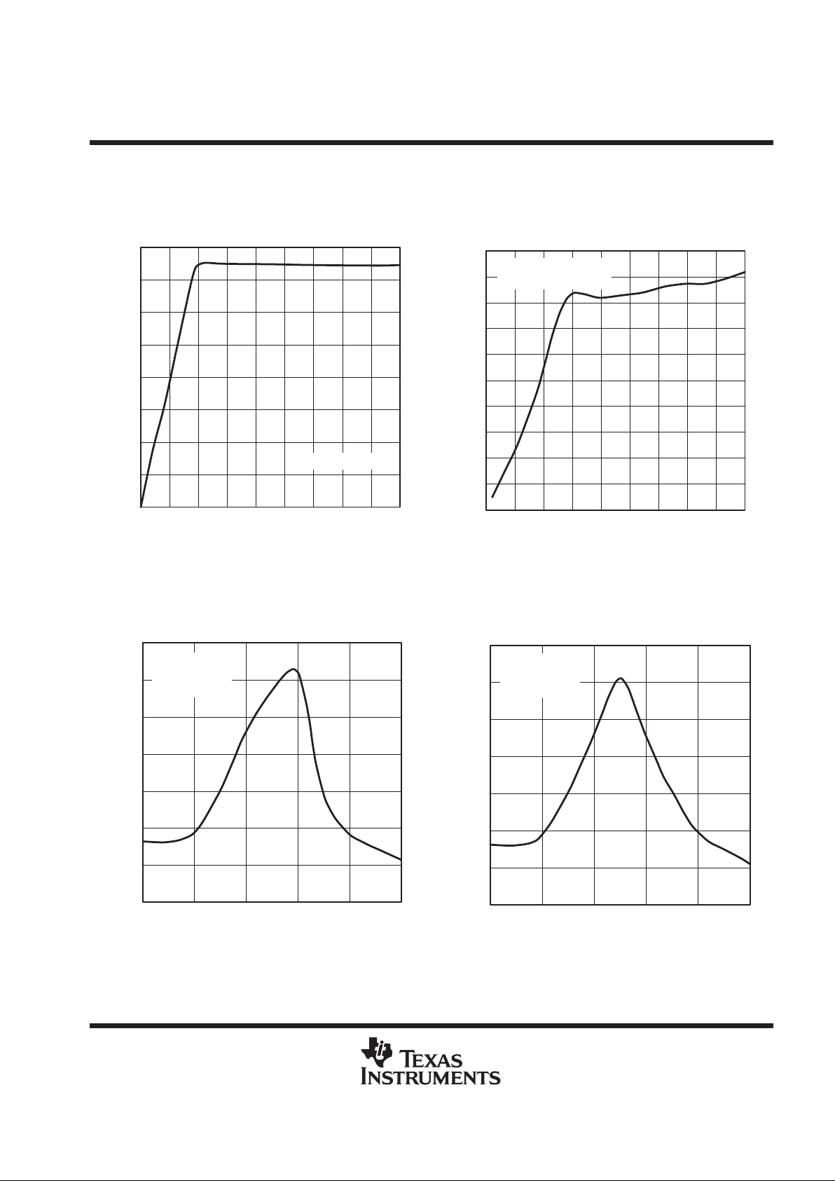
As shown in Figures 24 and 25, the TPS2817 turns on the TPS1 110 power switch in less than 20 ns and off in
25 ns.
2 V/div
2 V/div
12.5 ns/div
Q1 Gate
Q1 Drain
Figure 24. Q1 Turn-On Waveform
2 V/div
2 V/div
12.5 ns/div
Q1 Drain
Q1 Gate
Figure 25. Q1 Turn-Off Waveform
Page 18

TPS2816, TPS2817, TPS2818, TPS2819, TPS2828, TPS2829
SINGLE-CHANNEL HIGH-SPEED MOSFET DRIVER
SLVS160A – FEBRUARY 1997 – REVISED NOVEMBER 1997
18
POST OFFICE BOX 655303 • DALLAS, TEXAS 75265
APPLICATION INFORMATION
The efficiency for various output currents, with a 5.25-V input, is shown in Figure 26. For a 3.3-V output, the
efficiency is greater than 90% for loads up to 2 A – exceptional for a simple, inexpensive design.
80
75
70
0 0.5 1 1.5 2 2.5 3
Efficiency – %
85
90
Load Current – A
95
3.5 4 4.5 5
VO = 3.3 V
VO = 2.5 V
VI = 5.25 V
TA = 25°C
Figure 26. Converter Efficiency
Page 19
TPS2816, TPS2817, TPS2818, TPS2819, TPS2828, TPS2829
SINGLE-CHANNEL HIGH-SPEED MOSFET DRIVER
SLVS160A – FEBRUARY 1997 – REVISED NOVEMBER 1997
19
POST OFFICE BOX 655303 • DALLAS, TEXAS 75265
MECHANICAL DATA
DBV (R-PDSO-G5) PLASTIC SMALL-OUTLINE PACKAGE
0,25
Gage Plane
0,15 NOM
4073253-4/B 11/96
2,50
3,00
0,40
0,20
1,50
1,80
45
3
3,10
1
2,70
1,00
1,30
0,05 MIN
Seating Plane
0,95
M
0,25
0°–8°
0,10
NOTES: A. All linear dimensions are in millimeters.
B. This drawing is subject to change without notice.
C. Body dimensions include mold flash or protrusion.
Page 20

IMPORTANT NOTICE
T exas Instruments and its subsidiaries (TI) reserve the right to make changes to their products or to discontinue
any product or service without notice, and advise customers to obtain the latest version of relevant information
to verify, before placing orders, that information being relied on is current and complete. All products are sold
subject to the terms and conditions of sale supplied at the time of order acknowledgement, including those
pertaining to warranty, patent infringement, and limitation of liability.
TI warrants performance of its semiconductor products to the specifications applicable at the time of sale in
accordance with TI’s standard warranty. Testing and other quality control techniques are utilized to the extent
TI deems necessary to support this warranty. Specific testing of all parameters of each device is not necessarily
performed, except those mandated by government requirements.
CERT AIN APPLICATIONS USING SEMICONDUCTOR PRODUCTS MAY INVOLVE POTENTIAL RISKS OF
DEATH, PERSONAL INJURY, OR SEVERE PROPERTY OR ENVIRONMENTAL DAMAGE (“CRITICAL
APPLICATIONS”). TI SEMICONDUCTOR PRODUCTS ARE NOT DESIGNED, AUTHORIZED, OR
WARRANTED TO BE SUITABLE FOR USE IN LIFE-SUPPORT DEVICES OR SYSTEMS OR OTHER
CRITICAL APPLICATIONS. INCLUSION OF TI PRODUCTS IN SUCH APPLICA TIONS IS UNDERST OOD TO
BE FULLY AT THE CUSTOMER’S RISK.
In order to minimize risks associated with the customer’s applications, adequate design and operating
safeguards must be provided by the customer to minimize inherent or procedural hazards.
TI assumes no liability for applications assistance or customer product design. TI does not warrant or represent
that any license, either express or implied, is granted under any patent right, copyright, mask work right, or other
intellectual property right of TI covering or relating to any combination, machine, or process in which such
semiconductor products or services might be or are used. TI’s publication of information regarding any third
party’s products or services does not constitute TI’s approval, warranty or endorsement thereof.
Copyright 1998, Texas Instruments Incorporated
 Loading...