

* USB Requirement that downstream-facing ports
are bypassed with at least 120 F per hubm
IN
FAULT
EN
OUT
ILIM
GND
PowerPad
USBData
USB
Port
120 F*m
R
15k
ILIM
W
0.1 Fm
R
100k
FAULT
W
INPUT
5VUSB
FAULT Signal
ControlSignal
TPS2550/51
2
1
3
5
6
4
OUT
EN
GND
ILIM
FAULT
IN
TPS2550/TPS2551
DBVPACKAGE
(TOP VIEW)
TPS2550/TPS2551
DRVPACKAGE
(TOP VIEW)
2
1
3
5
6
4
OUT
EN
GND
ILIM
FAULT
IN
PAD
EN= ActiveLowfortheTPS2550
EN= ActiveHighfortheTPS2551
TPS2014600mA
TPS20151 A
TPS2041B500mA
TPS2051B500mA
TPS2045A 250mA
TPS2049100mA
TPS2055A 250mA
TPS20611 A
TPS20651 A
TPS20681.5 A
TPS20691.5 A
TPS2042B500mA
TPS2052B500mA
TPS2046B250mA
TPS2056250mA
TPS20621 A
TPS20661 A
TPS20601.5 A
TPS20641.5 A
TPS2080500mA
TPS2081500mA
TPS2082500mA
TPS2090250mA
TPS2091250mA
TPS2092250mA
TPS2043B500mA
TPS2053B500mA
TPS2047B250mA
TPS2057A 250mA
TPS20631 A
TPS20671 A
TPS2044B500mA
TPS2054B500mA
TPS2048A 250mA
TPS2058250mA
TPS2085500mA
TPS2086500mA
TPS2087500mA
TPS2095250mA
TPS2096250mA
TPS2097250mA
TPS201xA 0.2A to2 A
TPS202x0.2 A to2A
TPS203x0.2 A to2A
GENERAL SWITCHCATALOG
33m ,SingleW 80m ,SingleW
80m ,DualW 80m ,DualW
80m , TripleW
80m ,QuadW 80m ,QuadW
TPS2550
TPS2551
www.ti.com
SLVS736 – FEBRUARY 2008
ADJUSTABLE CURRENT-LIMITED POWER-DISTRIBUTION SWITCHES
1
FEATURES
• Adjustable Current-Limit, 100 mA – 1100 mA
• Fast Overcurrent Response - 2 µ S Typical
• 85-m Ω High-Side MOSFET (DBV Package)
• Reverse Input-Output Voltage Protection
• Operating Range: 2.5 V to 6.5 V
• Deglitched Fault Report
• 1- µ A Maximum Standby Supply Current
• Ambient Temperature Range: – 40 ° C to 85 ° C
• Built-in Soft-Start
• 15 kV ESD Protection (with external
capacitance) output load exceeds the current-limit threshold or a
APPLICATIONS
• USB Ports/Hubs
• Cell phones
• Laptops
• Heavy Capacitive Loads
• Reverse-Voltage Protection
DESCRIPTION
The TPS2550/51 power-distribution switch is
intended for applications where heavy capacitive
loads and short-circuits are likely to be encountered,
incorporating a 100-m Ω , N-channel MOSFET in a
single package. The current-limit threshold is user
adjustable between 100 mA and 1.1 A via an external
resistor. The power-switch rise and fall times are
controlled to minimize current surges during
switching.
The device limits the output current to a desired level
by switching into a constant-current mode when the
short is present. An internal reverse-voltage detection
comparator disables the power-switch in the event
that the output voltage is driven higher than the input
to protect devices on the input side of the switch. The
FAULT logic output asserts low during both
overcurrent and reverse-voltage conditions.
1
PRODUCTION DATA information is current as of publication date.
Products conform to specifications per the terms of the Texas
Instruments standard warranty. Production processing does not
necessarily include testing of all parameters.
Please be aware that an important notice concerning availability, standard warranty, and use in critical applications of
Texas Instruments semiconductor products and disclaimers thereto appears at the end of this data sheet.
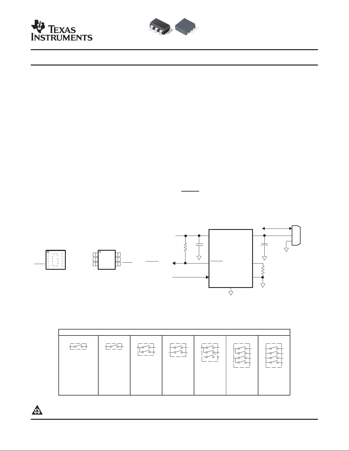
Figure 1. Typical Application as USB Power Switch
Copyright © 2008, Texas Instruments Incorporated
www.ti.com
TPS2550
TPS2551
SLVS736 – FEBRUARY 2008
This device contains circuits to protect its inputs and outputs against damage due to high static voltages or electrostatic fields.
These circuits have been qualified to protect this device against electrostatic discharges (ESD) of up to 2 kV according to
MIL-STD-883C, Method 3015; however, it is advised that precautions be taken to avoid application of any voltage higher than
maximum-rated voltages to these high-impedance circuits. During storage or handling the device leads should be shorted together
or the device should be placed in conductive foam. In a circuit, unused inputs should always be connected to an appropriate logic
voltage level, preferably either VCC or ground. Specific guidelines for handling devices of this type are contained in the publication
Guidelines for Handling Electrostatic-Discharge-Sensitive (ESDS) Devices and Assemblies available from Texas Instruments.
AVAILABLE OPTIONS AND ORDERING INFORMATION
DEVICE AMBIENT ENABLE SON
(1)
TEMPERATURE (DRV) (DBV) CONTINUOUS LOAD CURRENT
TPS2550 Active low TPS2550DRV TPS2550DBV 1.1 A
TPS2551 Active high TPS2551DRV TPS2551DBV 1.1 A
– 40 ° C to 85 ° C
(1) Add an R suffix to the device type for tape and reel.
(1)
SOT23
RECOMMENDED MAXIMUM
ABSOLUTE MAXIMUM RATINGS
over operating free-air temperature range unless otherwise noted
Voltage range on IN, OUT, EN or EN, ILIM, FAULT – 0.3 to 7 V
Voltage range from IN to OUT – 7 to 7 V
I
Continuous output current Internally limited
OUT
Continuous total power dissipation
FAULT sink current 25 mA
ILIM source current 1 mA
ESD
T
Maximum junction temperature – 40 to 150 ° C
J
T
Storage temperature – 65 to 150 ° C
Sgt
Lead temperature 1,6 mm (1/16-inch) from case for 10 seconds 300 ° C
(1) Stresses beyond those listed under absolute maximum ratings may cause permanent damage to the device. These are stress ratings
only, and functional operation of the device at these or any other conditions beyond those indicated under recommended operating
conditions is not implied. Exposure to absolute-maximum-rated conditions for extended periods may affect device reliability.
(2) Voltages are referenced to GND unless otherwise noted.
HBM 2 kV
CDM 500 V
(1) (2)
VALUE UNIT
See "Dissipation Rating
Table"
DISSIPATION RATING TABLE
BOARD PACKAGE THERMAL THERMAL TA≤ 25 ° C DERATING TA= 70 ° C TA= 85 ° C
(1)
Low-K
High-K
Low-K
High-K
DBV 350 ° C/W 55 ° C/W 285 mW 2.85 mW/ ° C 155 mW 114 mW
(2)
DBV 160 ° C/W 55 ° C/W 625 mW 6.25 mW/ ° C 340 mW 250 mW
(1)
DRV 140 ° C/W 20 ° C/W 715 mW 7.1 mW/ ° C 395 mW 285 mW
(2)
DRV 75 ° C/W 20 ° C/W 1330 mW 13.3 mW/ ° C 730 mW 530 mW
(1) The JEDEC low-K (1s) board used to derive this data was a 3in × 3in, two-layer board with 2-ounce copper traces on top of the board.
(2) The JEDEC high-K (2s2p) board used to derive this data was a 3in × 3in, multilayer board with 1-ounce internal power and ground
planes and 2-ounce copper traces on top and bottom of the board.
RESISTANCE RESISTANCE
θ
JA
θ
JC
RATING
TA= 25 ° C RATING RATING
POWER FACTOR ABOVE POWER POWER
2 Submit Documentation Feedback Copyright © 2008, Texas Instruments Incorporated
Product Folder Link(s): TPS2550 TPS2551
www.ti.com
RECOMMENDED OPERATING CONDITIONS
MIN MAX UNIT
V
IN
V
EN
V
/EN
I
OUT
R
ILIM
I
/FAULT
T
J
Input voltage, IN 2.5 6.5 V
Enable voltage V
TPS2550 0 6.5
TPS2551 0 6.5
Continuous output current, OUT 0 1.1 A
Current-limit set resistor from ILIM to GND 14.3 80.6 k Ω
FAULT sink current 0 10 mA
Operating virtual junction
temperature
DRV – 40 105
DBV – 40 125
ELECTRICAL CHARACTERISTICS
over recommended operating junction temperature range, 2.5 V ≤ V
(unless otherwise noted)
PARAMETER TEST CONDITIONS
POWER SWITCH
DBV package, TJ= 25 ° C 85 95
r
DS(on)
t
r
t
f
Static drain-source on-state resistance m Ω
Rise time, output
Fall time, output
ENABLE INPUT EN OR EN
V
V
I
EN
t
on
t
off
High-level input voltage 1.1
IH
Low-level input voltage 0.66
IL
Input current VEN= 0 V or 6.5 V, V
Turnon time 3 ms
Turnoff time 3 ms
CURRENT LIMIT
I
OS
I
OC
t
IOS
Short-circuit current, OUT connected to GND R
Current-limit threshold (Maximum DC output current I
Response time to short circuit VIN= 5.0 V (see Figure 3 ) 2 µ s
REVERSE-VOLTAGE PROTECTION
Reverse-voltage comparator trip point
(V
– VIN)
OUT
Time from reverse-voltage condition to
MOSFET turn off
SUPPLY CURRENT
I
IN_off
I
IN_on
I
REV
Supply current, low-level output 0.1 1 µ A
Supply current, high-level output
Reverse leakage current V
(1) Pulse-testing techniques maintain junction temperature close to ambient temperature; thermal effects must be taken into account
separately.
DBV package, – 40 ° C ≤ TJ≤ 125 ° C 135
DRV package, TJ= 25 ° C 100 115
DRV package, – 40 ° C ≤ TJ≤ 105 ° C 145
VIN= 6.5 V 1.0 1.5
VIN= 2.5 V 0.65 1.0
VIN= 6.5 V 0.2 0.5
VIN= 2.5 V 0.2 0.5
/EN
CL= 1 µ F, RL= 100 Ω , (see Figure 2 )
delivered to load) R
OUT
VIN= 5.0 V 3 5 7 ms
VIN= 6.5 V, No load on OUT, VEN= 6.5 V or VEN= 0 V, 14.3 k Ω
≤ R
≤ 80.6 k Ω
ILIM
VIN= 6.5 V, No load on OUT, VEN= 0 V or
VEN= 6.5 V
= 6.5 V, VIN= 0 V TJ= 25 ° C 0.01 1 µ A
OUT
≤ 6.5 V, R
IN
ILIM
(1)
= 14.3 k Ω , V
= 0 V, or V
/EN
MIN TYP MAX UNIT
CL= 1 µ F, RL= 100 Ω ,
(see Figure 2 )
= 0 V or 6.5 V – 0.5 0.5 µ A
R
= 80.6 k Ω 110 215 300
ILIM
= 38.3 k Ω 300 500 650
ILIM
R
= 15 k Ω 1050 1400 1650
ILIM
R
= 80.6 k Ω 290 315 340
ILIM
= 38.3 k Ω 620 665 705
ILIM
R
= 15 k Ω 1550 1650 1750
ILIM
95 135 190 mV
R
= 15 k Ω 150 µ A
ILIM
R
= 80.6 k Ω 130 µ A
ILIM
TPS2550
TPS2551
SLVS736 – FEBRUARY 2008
= 5.0 V
EN
° C
ms
V
mA
Copyright © 2008, Texas Instruments Incorporated Submit Documentation Feedback 3
Product Folder Link(s): TPS2550 TPS2551
www.ti.com
TPS2550
TPS2551
SLVS736 – FEBRUARY 2008
ELECTRICAL CHARACTERISTICS (continued)
over recommended operating junction temperature range, 2.5 V ≤ V
(unless otherwise noted)
PARAMETER TEST CONDITIONS
UNDERVOLTAGE LOCKOUT
V
FAULT FLAG
V
THERMAL SHUTDOWN
Low-level input voltage, IN VINrising 2.35 2.45 V
UVLO
Hysteresis, IN TJ= 25 ° C 25 mV
Output low voltage, FAULT I
OL
Off-state leakage V
FAULT deglitch
Thermal shutdown threshold 155 ° C
Thermal shutdown threshold in current-limit 135 ° C
Hysteresis 15 ° C
= 1 mA 180 mV
/FAULT
= 6.5 V 1 µ A
/FAULT
FAULT assertion or de-assertion due to overcurrent condition 5 7.5 10 ms
FAULT assertion or de-assertion due to reverse-voltage
condition
≤ 6.5 V, R
IN
ILIM
(1)
= 14.3 k Ω , V
= 0 V, or V
/EN
MIN TYP MAX UNIT
2 4 6 ms
= 5.0 V
EN
4 Submit Documentation Feedback Copyright © 2008, Texas Instruments Incorporated
Product Folder Link(s): TPS2550 TPS2551
www.ti.com
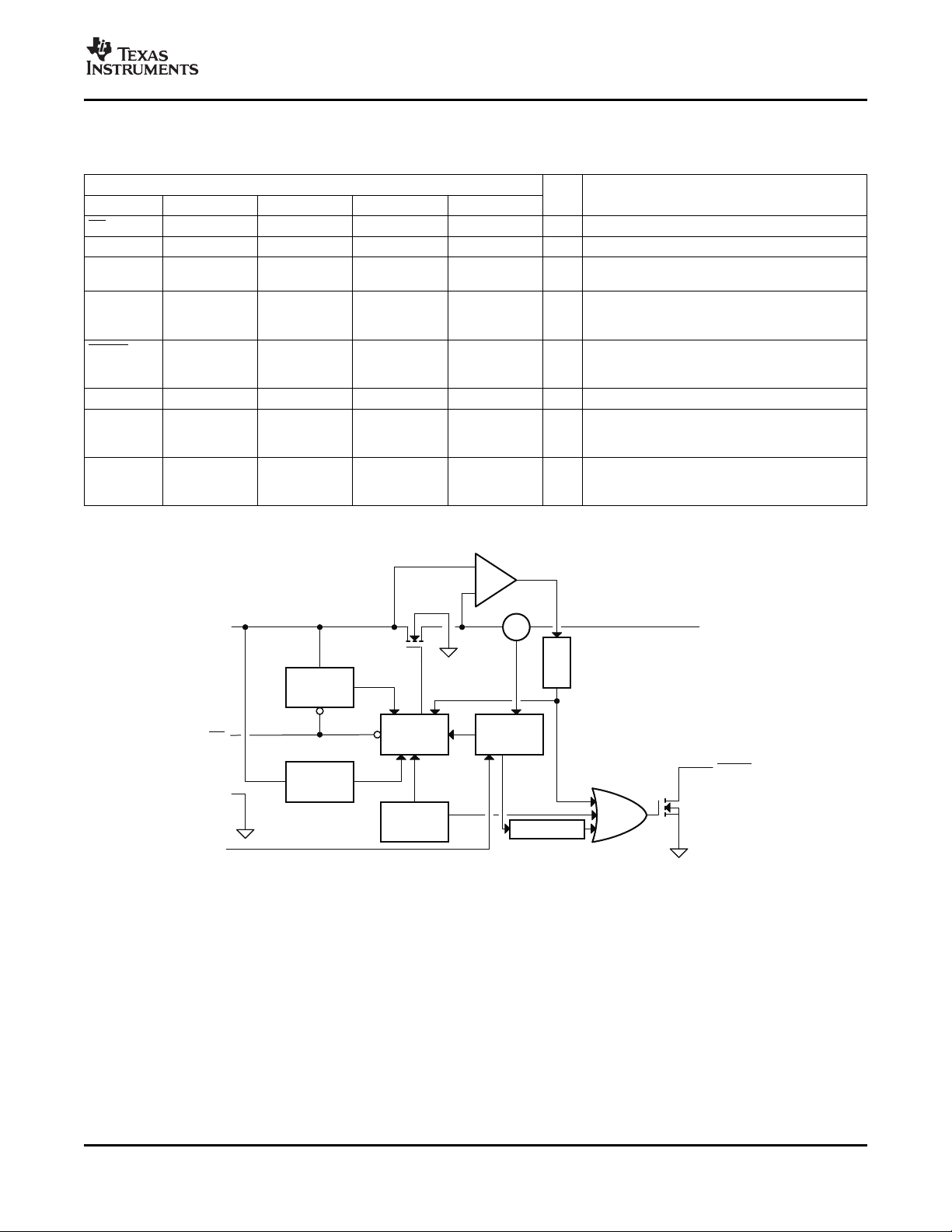
Charge
Pump
Driver
UVLO
Current
Limit
Thermal
Sense
IN
GND
EN
ILIM
OUT
FAULT
CS
Reverse
Voltage
Comparator
-
+
Current
Sense
4-ms
Deglitch
8-msDeglitch
TPS2550
TPS2551
SLVS736 – FEBRUARY 2008
DEVICE INFORMATION
Terminal Functions
TERMINAL
NAME TPS2550DBV TPS2551DBV TPS2550DRV TPS2551DRV
EN 3 – 4 – I Enable input, logic low turns on power switch
EN – 3 – 4 I Enable input, logic high turns on power switch
GND 2 2 5 5 Ground connection; should be connected
IN 1 1 6 6 I Input voltage; connect a 0.1 µ F or greater
FAULT 4 4 3 3 O Active-low open-drain output, asserted during
OUT 6 6 1 1 O Power-switch output
ILIM 5 5 2 2 I External resistor used to set current-limit
POWER – – PAD PAD Internally connected to GND; used to heat-sink
PAD the part to the circuit board traces. Should be
I/O DESCRIPTION
externally to POWER PAD
ceramic capacitor from IN to GND as close to the
IC as possible.
overcurrent, overtemperature, or reverse-voltage
conditions.
threshold; recommended 14.3 k Ω ≤ R
k Ω .
connected to GND pin.
ILIM
≤ 80.6
FUNCTIONAL BLOCK DIAGRAM
Copyright © 2008, Texas Instruments Incorporated Submit Documentation Feedback 5
Product Folder Link(s): TPS2550 TPS2551
www.ti.com
R
L
C
L
OUT
t
r
t
f
90%
90%
10%
10%
50%
50%
90%
10%
V
EN
V
OUT
VOLTAGEWAVEFORMS
TESTCIRCUIT
t
on
t
off
50%
50%
90%
10%
t
on
t
off
V
OUT
V
OUT
V
EN
t
IOS
I
OS
I
OUT
I
OUT
I
OS
I
OC
DECREASING
LOAD
RESISTANCE
V
OUT
DECREASING
LOAD
RESISTANCE
TPS2550
TPS2551
SLVS736 – FEBRUARY 2008
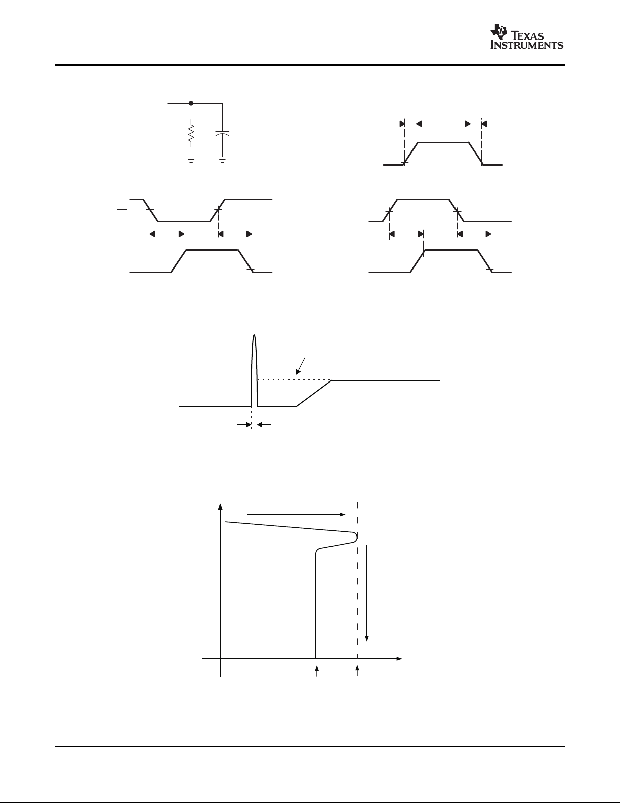
PARAMETER MEASUREMENT INFORMATION
Figure 2. Test Circuit and Voltage Waveforms
Figure 3. Response Time to Short-Circuit Waveform
Figure 4. Output Voltage vs. Current-Limit Threshold
Product Folder Link(s): TPS2550 TPS2551
6 Submit Documentation Feedback Copyright © 2008, Texas Instruments Incorporated
www.ti.com
TPS2550
TPS2551
SLVS736 – FEBRUARY 2008
TYPICAL CHARACTERISTICS
Figure 5. Turnon Delay and Rise Time
Figure 6. Turnoff Delay and Fall Time
Copyright © 2008, Texas Instruments Incorporated Submit Documentation Feedback 7
Product Folder Link(s): TPS2550 TPS2551
www.ti.com
TPS2550
TPS2551
SLVS736 – FEBRUARY 2008
TYPICAL CHARACTERISTICS (continued)
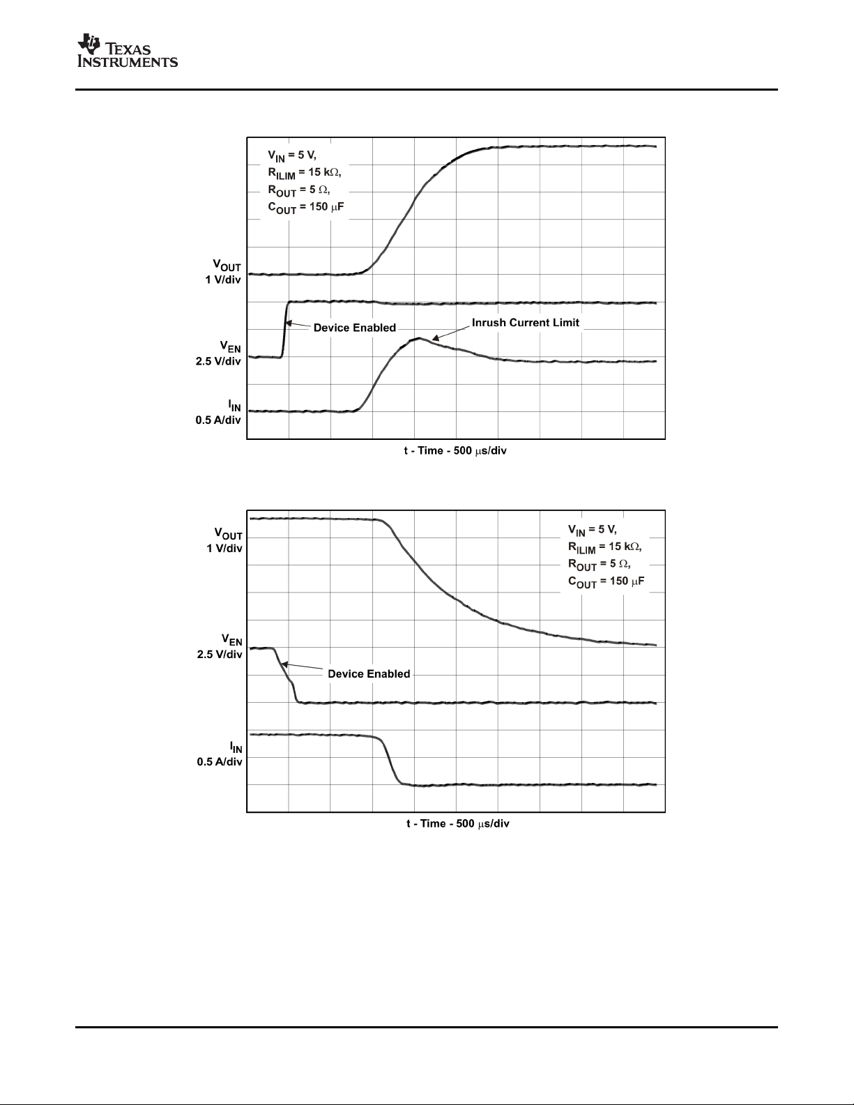
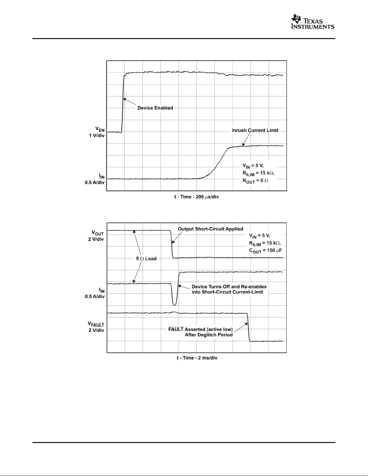
Figure 7. Device Enabled into Short-Circuit
Figure 8. Full-Load to Short-Circuit Transient Response
8 Submit Documentation Feedback Copyright © 2008, Texas Instruments Incorporated
Product Folder Link(s): TPS2550 TPS2551
www.ti.com
TYPICAL CHARACTERISTICS (continued)
TPS2550
TPS2551
SLVS736 – FEBRUARY 2008
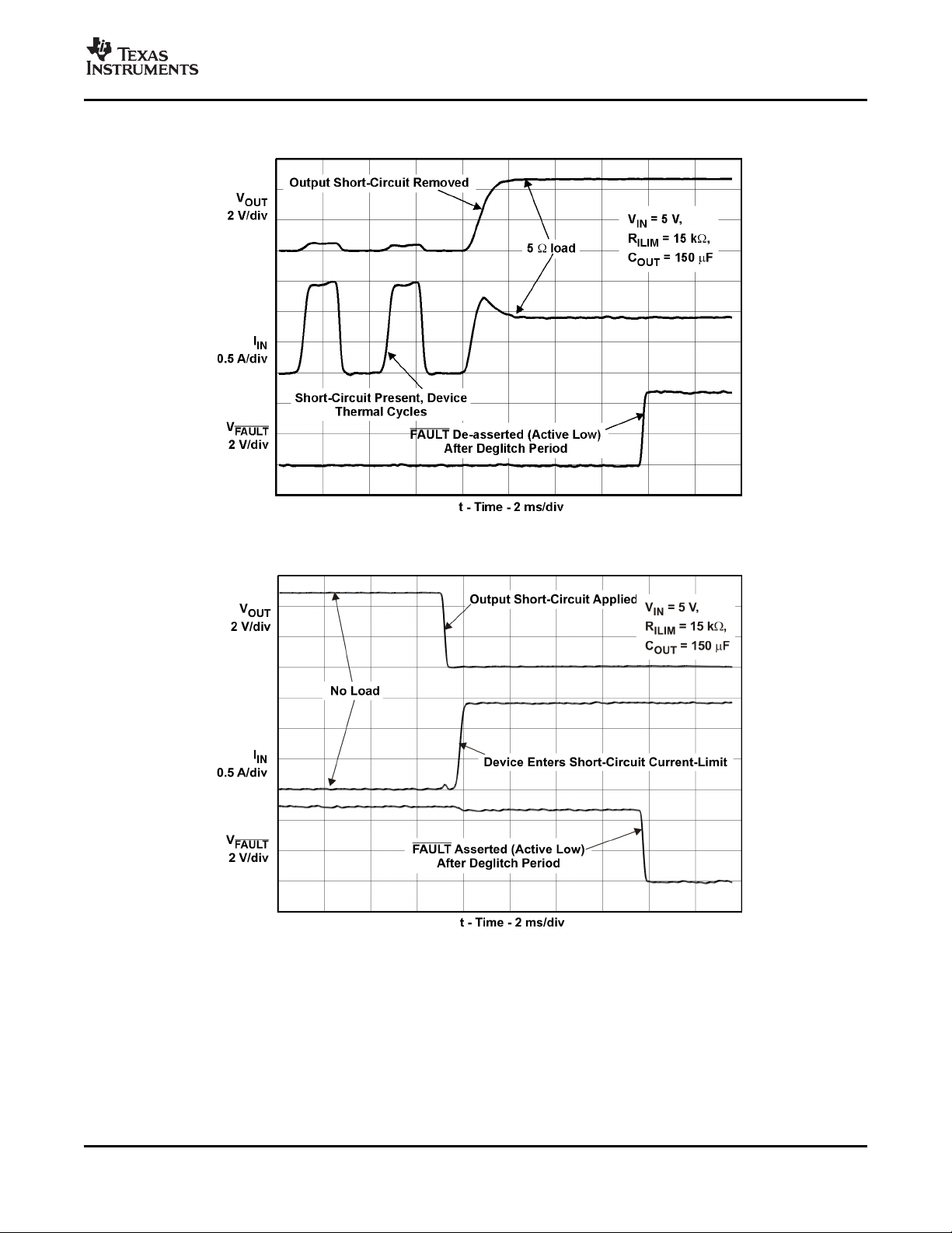
Figure 9. Short-Circuit to Full-Load Recovery Response
Figure 10. No-Load to Short-Circuit Transient Response
Copyright © 2008, Texas Instruments Incorporated Submit Documentation Feedback 9
Product Folder Link(s): TPS2550 TPS2551
www.ti.com
TPS2550
TPS2551
SLVS736 – FEBRUARY 2008
TYPICAL CHARACTERISTICS (continued)
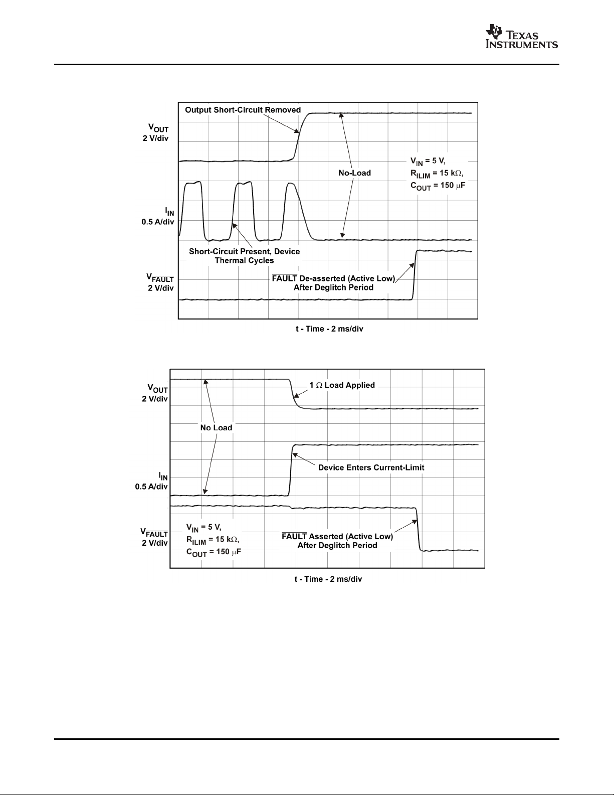
Figure 11. Short-Circuit to No-Load Recovery Response
Figure 12. No Load to 1 Ω Transient Response
10 Submit Documentation Feedback Copyright © 2008, Texas Instruments Incorporated
Product Folder Link(s): TPS2550 TPS2551

www.ti.com
TYPICAL CHARACTERISTICS (continued)
TPS2550
TPS2551
SLVS736 – FEBRUARY 2008
Figure 13. 1 Ω to No Load Transient Response
Figure 14. Reverse-Voltage Protection Response
Copyright © 2008, Texas Instruments Incorporated Submit Documentation Feedback 11
Product Folder Link(s): TPS2550 TPS2551

www.ti.com
2.30
UVLOFalling
T -JunctionTemperature-°C
J
-50 0 50 100 150
2.40
2.31
2.32
2.33
2.34
2.35
2.36
2.37
2.38
2.39
UVLORising
UVLO-UndervoltageLockout-V
TPS2550
TPS2551
SLVS736 – FEBRUARY 2008
TYPICAL CHARACTERISTICS (continued)
Figure 15. Reverse-Voltage Protection Recovery
Figure 16. UVLO – Undervoltage Lockout – V
12 Submit Documentation Feedback Copyright © 2008, Texas Instruments Incorporated
Product Folder Link(s): TPS2550 TPS2551

www.ti.com
0
T -JunctionTemperature-°C
J
-50 0 50 100 150
0.50
0.05
0.10
0.15
0.20
0.25
0.30
0.35
0.40
0.45
IIN-SupplyCurrent,OutputDisabled- Am
V =6.5V
IN
V =5V
IN
V =3.3V
IN
V =2.5V
IN
0
T -JunctionTemperature-°C
J
-50 0 50 100 150
150
15
30
45
60
75
90
105
120
135
IIN-SupplyCurrent,OutputEnabled- Am
V =5V
IN
V =3.3V
IN
V =2.5V
IN
V =6.5V
IN
R =20k
ILIM
W
TYPICAL CHARACTERISTICS (continued)
TPS2550
TPS2551
SLVS736 – FEBRUARY 2008
Figure 17. IIN– Supply Current, Output Disabled – µ A
Figure 18. IIN– Supply Current, Output Enabled – µ A
Copyright © 2008, Texas Instruments Incorporated Submit Documentation Feedback 13
Product Folder Link(s): TPS2550 TPS2551

www.ti.com
0
PeakCurrent- A
0 1.5 3 4.5 6
20
2
4
6
8
10
12
14
16
18
CurrentLimitResponse- sm
V =5V,
T =25°C
IN
A
0
T -JunctionTemperature-°C
J
-50 0 50 100 150
25
50
75
100
125
150
r -StaticDrain-SourceOn-StateResistance-m
DS(on)
W
DRVPackage
DBVPackage
TPS2550
TPS2551
SLVS736 – FEBRUARY 2008
TYPICAL CHARACTERISTICS (continued)
Figure 20. MOSFET r
Figure 19. Current Limit Response – µ s
Vs. Junction Temperature
DS(on)
14 Submit Documentation Feedback Copyright © 2008, Texas Instruments Incorporated
Product Folder Link(s): TPS2550 TPS2551

www.ti.com
TPS2550
TPS2551
SLVS736 – FEBRUARY 2008
DETAILED DESCRIPTION
OVERVIEW
The TPS2550/51 are current-limited, power distribution switches using N-channel MOSFETs for applications
where short-circuits or heavy capacitive loads will be encountered. These devices allow the user to program the
current-limit threshold between 100 mA and 1.1 A via an external resistor. Additional device shutdown features
include overtemperature protection and reverse-voltage protection. The device incorporates an internal charge
pump and gate drive circuitry necessary to drive the N-channel MOSFET. The charge pump supplies power to
the driver circuit and provides the necessary voltage to pull the gate of the MOSFET above the source. The
charge pump operates from input voltages as low as 2.5 V and requires little supply current. The driver controls
the gate voltage of the power switch. The driver incorporates circuitry that controls the rise and fall times of the
output voltage to limit large current and voltage surges and provide built-in soft-start functionality.
OVERCURRENT
The TPS2550/51 responds to an overcurrent condition by limiting its output current to the I
shown in Figure 21 . Three response profiles are possible depending on the loading conditions and are
summarized in Figure 4 .
One response profile occurs if the TPS2550/51 is enabled into a short-circuit. The output voltage is held near
zero potential with respect to ground and the TPS2550/51 ramps the output current to IOS(see Figure 7 ).
A second response profile occurs if a short is applied to the output after the TPS2550/51 is enabled. The device
responds to the overcurrent condition within time t
(see Figure 3 ). The current-sense amplifier is over-driven
IOS
during this time and momentarily disables the internal current-limit MOSFET. The current-sense amplifier
gradually recovers and limits the output current to IOS.
A third response profile occurs if the load current gradually increases. The device first limits the load current to
IOC. If the load demands a current greater than IOC, the TPS2550/51 folds back the current to IOSand the output
voltage decreases to IOSx R
for a resistive load, which is shown in Figure 4 .
LOAD
The TPS2550/51 thermal cycles if an overload condition is present long enough to activate thermal limiting in any
of the above cases. The device turns off when the junction temperature exceeds 135 ° C (typ). The device
remains off until the junction temperature cools 15 ° C (typ) and then restarts. The TPS2550/51 cycles on/off until
the overload is removed (see Figure 9 and Figure 11 ) .
and I
OC
levels
OS
REVERSE-VOLTAGE PROTECTION
The reverse-voltage protection feature turns off the N-channel MOSFET whenever the output voltage exceeds
the input voltage by 135 mV (typical) for 4-ms. This prevents damage to devices on the input side of the
TPS2550/51 by preventing significant current from sinking into the input capacitance. The N-channel MOSFET is
allowed to turn-on once the output voltage goes below the input voltage for the same 4-ms deglitch time. The
reverse-voltage comparator also asserts the FAULT output (active-low) after 4-ms.
FAULT RESPONSE
The FAULT open-drain output is asserted (active low) during an overcurrent, overtemperature or reverse-voltage
condition. The output remains asserted until the fault condition is removed. The TPS2550/51 is designed to
eliminate false FAULT reporting by using an internal delay "deglitch" circuit for overcurrent (7.5-ms) and
reverse-voltage (4-ms) conditions without the need for external circuitry. This ensures that FAULT is not
accidentally asserted due to normal operation such as starting into a heavy capacitive load. The deglitch circuitry
delays entering and leaving fault conditions. Overtemperature conditions are not deglitched and assert the
FAULT signal immediately.
UNDERVOLTAGE LOCKOUT (UVLO)
The undervoltage lockout (UVLO) circuit disables the power switch until the input voltage reaches the UVLO
turn-on threshold. Built-in hysteresis prevents unwanted on/off cycling due to input voltage drop from large
current surges.
Copyright © 2008, Texas Instruments Incorporated Submit Documentation Feedback 15
Product Folder Link(s): TPS2550 TPS2551

www.ti.com
TPS2550
TPS2551
SLVS736 – FEBRUARY 2008
ENABLE ( EN OR EN)
The logic enable controls the power switch, bias for the charge pump, driver, and other circuits to reduce the
supply current. The supply current is reduced to less than 1- µ A when a logic high is present on EN or when a
logic low is present on EN. A logic low input on EN or a logic high input on EN enables the driver, control circuits,
and power switch. The enable input is compatible with both TTL and CMOS logic levels.
THERMAL SENSE
The TPS2550/51 protects itself with two independent thermal sensing circuits that monitor the operating
temperature of the power-switch and disables operation if the temperature exceeds recommended operating
conditions. The device operates in constant-current mode during an overcurrent conditions, which increases the
voltage drop across power-switch. The power dissipation in the package is proportional to the voltage drop
across the power-switch, so the junction temperature rises during an overcurrent condition. The first thermal
sensor turns off the power-switch when the die temperature exceeds 135 ° C and the part is in current limit. The
second thermal sensor turns off the power-switch when the die temperature exceeds 155 ° C regardless of
whether the power-switch is in current limit. Hysteresis is built into both thermal sensors, and the switch turns on
after the device has cooled approximately 15 ° C. The switch continues to cycle off and on until the fault is
removed. The open-drain false reporting output FAULT is asserted (active low) immediately during an
overtemperature shutdown condition.
16 Submit Documentation Feedback Copyright © 2008, Texas Instruments Incorporated
Product Folder Link(s): TPS2550 TPS2551

www.ti.com
TPS2550
TPS2551
SLVS736 – FEBRUARY 2008
APPLICATION INFORMATION
INPUT AND OUTPUT CAPACITANCE
Input and output capacitance improve the performance of the device; the actual capacitance should be optimized
for the particular application. For all applications, a 0.01 µ F to 0.1 µ F ceramic bypass capacitor between IN and
GND is recommended as close to the device as possible for local noise de-coupling. This precaution reduces
ringing on the input due to power-supply transients. Additional input capacitance may be needed on the input to
reduce voltage overshoot from exceeding the absolute maximum voltage of the device during heavy transients.
This is especially important during bench testing when long, inductive cables are used to connect the evaluation
board to the bench power-supply.
Placing a high-value electrolytic capacitor on the output pin is recommended when the large transient currents
are expected on the output. Additionally, bypassing the output with a 0.01 µ F to 0.1 µ F ceramic capacitor
improves the immunity of the device to short-circuit transients.
PROGRAMMING THE CURRENT-LIMIT THRESHOLD
The overcurrent threshold is user programmable via an external resistor. Many applications require that the
minimum current-limit is above a certain current level or that the maximum current-limit is below a certain current
level, so it is important to consider the tolerance of the overcurrent threshold when selecting a value for R
The following equations and Figure 21 can be used to calculate the resulting overcurrent threshold for a given
external resistor value (R
and process. The traces routing the R
parasitic effects on the current-limit accuracy.
There are two important current-limit thresholds for the device and are related by Figure 4 . The first threshold is
the short-circuit current threshold IOS. I
short-circuit or a short-circuit is applied during normal operation. The second threshold is the overcurrent
threshold IOC. I
current. I
OC
consider both I
is the peak DC current that can be delivered to the load before the device begins to limit
OC
is important if ramped loads or slow transients are common to the application. It is important to
and I
OS
occurs 1) above a minimum load current or 2) below a maximum load current.
To design above a minimum current-limit threshold, find the intersection of R
current on the I
OS(min)
minimum threshold is important to ensure start-up into full-load or heavy capacative loads. The resulting
maximum DC load current is the intersection of the selected value of R
To design below a maximum DC current level, find the intersection of R
current on the I
OC(max)
maximum threshold is important to avoid current-limiting upstream power supplies causing the input voltage bus
to droop. The resulting minimum short-circuit current is the intersection of the selected value of R
I
curve.
OS(min)
). Figure 21 includes current-limit tolerance due to variations caused by temperature
ILIM
when choosing R
OC
curve and choose a value of R
curve and choose a value of R
resistor to the TPS2550/51should be as short as possible to reduce
ILIM
is the current delivered to the load if the part is enabled into a
OS
. R
ILIM
can be selected to provide a current-limit threshold that
ILIM
below this value. Programming the current-limit above a
ILIM
ILIM
above this value. Programming the current-limit below a
ILIM
and the maximum desired load
ILIM
and the I
ILIM
OC(max)
and the maximum desired load
curve.
and the
ILIM
.
ILIM
Overcurrent Threshold Equations (I
• I
• I
• I
OC(max)
OC(typ)
OC(min)
(mA) = (24500 V) / (R
(mA) = (23800 V) / (R
(mA) = (23100 V) / (R
Short-Circuit Current Equations (I
• I
OS(max)
• I
OS(typ)
• I
OS(min)
where 14.3 k Ω ≤ R
Copyright © 2008, Texas Instruments Incorporated Submit Documentation Feedback 17
(mA) = (25500 V) / (R
(mA) = (28700 V) / (R
(mA) = (39700 V) / (R
≤ 80.6 k Ω . I
ILIM
):
OC
ILIM
ILIM
ILIM
):
OS
ILIM
ILIM
ILIM
OS(typ)
0.975
k Ω )
0.985
k Ω )
0.996
k Ω )
1.013
k Ω )
1.114
k Ω )
1.342
k Ω )
and I
Product Folder Link(s): TPS2550 TPS2551
OS(max)
are not plotted to improve graph clarity.

www.ti.com
0
100
200
300
400
500
600
700
800
900
1000
1100
1200
1300
1400
1500
1600
1700
1800
15 20 25 30 35 40 45 50 55 60 65 70 75 80
R -k
ILIM
W
Current-LimitThreshold-mA
I
OC(max)
I
OC(typ)
I
OC(min)
I
OS(min)
TPS2550
TPS2551
SLVS736 – FEBRUARY 2008
Figure 21. Current-Limit Threshold Vs.R
APPLICATION 1: DESIGNING ABOVE A MINIMUM CURRENT-LIMIT
Some applications require that current-limiting cannot occur below a certain threshold. For this example, assume
that 1 A must be delivered to the load so that the minimum desired current-limit threshold is 1000 mA. Use the
IOSequations and Figure 21 to select R
• I
• I
• R
• R
(mA) = 1000 mA
OS(min)
(mA) = (39700 V) / (R
OS(min)
(k Ω ) = [(39700 V) / (I
ILIM
= 15.54 k Ω
ILIM
ILIM
OS(min)
Select the closest 1% resistor less than the calculated value: R
threshold at 1 A . Use the IOCequations, Figure 21 , and the previously calculated value for R
maximum resulting current-limit threshold.
• R
• I
• I
• I
The resulting maximum current-limit theshold is 1.7 A with a 15.4 k Ω resistor.
APPLICATION 2: DESIGNING BELOW A MAXIMUM CURRENT-LIMIT
Some applications require that current-limiting must occur below a certain threshold. For this example, assume
that the desired upper current-limit threshold must be below 1.25 A to protect an up-stream power supply. Use
the IOCequations and Figure 21 to select R
• I
• I
• R
• R
18 Submit Documentation Feedback Copyright © 2008, Texas Instruments Incorporated
= 15.4 k Ω
ILIM
OC(max)
OC(max)
OC(max)
OC(max)
OC(max)
(mA) = (24500 V) / (R
(mA) = (24500 V) / (15 (k Ω ))
= 1703 mA
(mA) = 1250 mA
(mA) = (24500 V) / (R
(k Ω ) = [(24500 V) / (I
ILIM
= 21.15 k Ω
ILIM
ILIM
ILIM
OC(max)
.
ILIM
1.342
(k Ω ))
(mA))]
1/1.342
0.975
(k Ω ))
0.975
.
ILIM
0.975
(k Ω ))
(mA))]
1/0.975
Product Folder Link(s): TPS2550 TPS2551
ILIM
= 15.4 k Ω . This sets the minimum current-limit
ILIM
ILIM
to calculate the

www.ti.com
TPS2550
TPS2551
SLVS736 – FEBRUARY 2008
Select the closest 1% resistor greater than the calculated value: R
= 21.5 k Ω . This sets the maximum
ILIM
current-limit threshold at 1.25 A . Use the IOSequations, Figure 21 , and the previously calculated value for R
to calculate the minimum resulting current-limit threshold.
• R
• I
• I
• I
= 21.5 k Ω
ILIM
(mA) = (39700 V) / (R
OS(min)
(mA) = (39700 V) / (21.5 (k Ω ))
OS(min)
= 647 mA
OS(min)
ILIM
1.342
1.342
(k Ω ))
The resulting minimum current-limit threshold is 647 mA with a 21.5 k Ω resistor.
POWER DISSIPATION AND JUNCTION TEMPERATURE
The low on-resistance of the N-channel MOSFET allows small surface-mount packages to pass large currents. It
is good design practice to estimate power dissipation and junction temperature. The below analysis gives an
approximation for calculating junction temperature based on the power dissipation in the package. However, it is
important to note that thermal analysis is strongly dependent on additional system level factors. Such factors
include air flow, board layout, copper thickness and surface area, and proximity to other devices dissipating
power. Good thermal design practice must include all system level factors in addition to individual component
analysis.
Begin by determining the r
temperature. As an initial estimate, use the highest operating ambient temperature of interest and read r
from the typical characteristics graph. Using this value, the power dissipation can be calculated by:
P
= r
D
DS(on)
2
× I
OUT
Where:
P
= Total power dissipation (W)
D
r
= Power switch on-resistance ( Ω )
DS(on)
I
= Maximum current-limit threshold (A)
OUT
This step calculates the total power dissipation of the N-channel MOSFET.
Finally, calculate the junction temperature:
TJ= P
× R
D
+ T
Θ JA
A
Where:
TA= Ambient temperature ( ° C)
R
= Thermal resistance ( ° C/W)
Θ JA
P
= Total power dissipation (W)
D
Compare the calculated junction temperature with the initial estimate. If they are not within a few degrees, repeat
the calculation using the "refined" r
iterations are generally sufficient to achieve the desired result. The final junction temperature is highly dependent
on thermal resistance R
, and thermal resistance is highly dependent on the individual package and board
θ JA
layout. The "Dissipating Rating Table" at the begginng of this document provides example thermal resistances for
specific packages and board layouts.
of the N-channel MOSFET relative to the input voltage and operating
DS(on)
from the previous calculation as the new estimate. Two or three
DS(on)
DS(on)
ILIM
UNIVERSAL SERIAL BUS (USB) POWER-DISTRIBUTION REQUIREMENTS
One application for this device is for current-limiting in universal serial bus (USB) applications. The original USB
interface was a 12-Mb/s or 1.5-Mb/s, multiplexed serial bus designed for low-to-medium bandwidth PC
peripherals (e.g., keyboards, printers, scanners, and mice). As the demand for more bandwidth increased, the
USB 2.0 standard was introduced increasing the maximum data rate to 480-Mb/s. The four-wire USB interface is
conceived for dynamic attach-detach (hot plug-unplug) of peripherals. Two lines are provided for differential data,
and two lines are provided for 5-V power distribution.
USB data is a 3.3-V level signal, but power is distributed at 5 V to allow for voltage drops in cases where power
is distributed through more than one hub across long cables. Each function must provide its own regulated 3.3 V
from the 5-V input or its own internal power supply. The USB specification classifies two different classes of
Copyright © 2008, Texas Instruments Incorporated Submit Documentation Feedback 19
Product Folder Link(s): TPS2550 TPS2551

www.ti.com
TPS2550
TPS2551
SLVS736 – FEBRUARY 2008
devices depending on its maximum current draw. A device classified as low-power can draw up to 100 mA as
defined by the standard. A device classified as high-power can draw up to 500 mA. It is important that the
minimum current-limit threshold of the current-limiting power-switch exceed the maximum current-limit draw of
the intended application. The latest USB standard should always be referenced when considering the
current-limit threshold
The USB specification defines two types of devices as hubs and functions. A USB hub is a device that contains
multiple ports for different USB devices to connect and can be self-powered (SPH) or bus-powered (BPH). A
function is a USB device that is able to transmit or receive data or control information over the bus. A USB
function can be embedded in a USB hub. A USB function can be one of three types included in the list below.
• Low-power, bus-powered function
• High-power, bus-powered function
• Self-powered function
SPHs and BPHs distribute data and power to downstream functions. The TPS2550/51 has higher current
capability than required for a single USB port allowing it to power multiple downstream ports.
SELF-POWERED AND BUS-POWERED HUBS
A SPH has a local power supply that powers embedded functions and downstream ports. This power supply
must provide between 4.75 V to 5.25 V to downstream facing devices under full-load and no-load conditions.
SPHs are required to have current-limit protection and must report overcurrent conditions to the USB controller.
Typical SPHs are desktop PCs, monitors, printers, and stand-alone hubs.
A BPH obtains all power from an upstream port and often contains an embedded function. It must power up with
less than 100 mA. The BPH usually has one embedded function, and power is always available to the controller
of the hub. If the embedded function and hub require more than 100 mA on power up, the power to the
embedded function may need to be kept off until enumeration is completed. This is accomplished by removing
power or by shutting off the clock to the embedded function. Power switching the embedded function is not
necessary if the aggregate power draw for the function and controller is less than 100 mA. The total current
drawn by the bus-powered device is the sum of the current to the controller, the embedded function, and the
downstream ports, and it is limited to 500 mA from an upstream port.
LOW-POWER BUS-POWERED AND HIGH-POWER BUS-POWERED FUNCTIONS
Both low-power and high-power bus-powered functions obtain all power from upstream ports. Low-power
functions always draw less than 100 mA; high-power functions must draw less than 100 mA at power up and can
draw up to 500 mA after enumeration. If the load of the function is more than the parallel combination of 44 Ω
and 10 µ F at power up, the device must implement inrush current limiting.
USB POWER-DISTRIBUTION REQUIREMENTS
USB can be implemented in several ways regardless of the type of USB device being developed. Several
power-distribution features must be implemented.
• SPHs must:
– Current-limit downstream ports
– Report overcurrent conditions
• BPHs must:
– Enable/disable power to downstream ports
– Power up at <100 mA
– Limit inrush current (<44 Ω and 10 µ F)
• Functions must:
– Limit inrush currents
– Power up at <100 mA
The feature set of the TPS2550/51 meets each of these requirements. The integrated current-limiting and
overcurrent reporting is required by self-powered hubs. The logic-level enable and controlled rise times meet the
need of both input and output ports on bus-powered hubs and the input ports for bus-powered functions.
20 Submit Documentation Feedback Copyright © 2008, Texas Instruments Incorporated
Product Folder Link(s): TPS2550 TPS2551

www.ti.com
OUT
IN
GND
FAULT
ILIM
EN
Input
TPS2551
PowerPad
Output
0.1 Fm
R
100k
FAULT
W
C
0.1 F
RETRY
m
R
20k
ILIM
W
C
LOAD
R
LOAD
1kW
OUT
IN
GND
FAULT
ILIM
EN
ExternalLogic
Signal&Driver
TPS2551
PowerPad
Input
0.1 Fm
R
100k
FAULT
W
C
0.1 F
RETRY
m
R
20k
ILIM
W
C
LOAD
R
LOAD
1kW
Output
TPS2550
TPS2551
SLVS736 – FEBRUARY 2008
AUTO-RETRY FUNCTIONALITY
Some applications require that an overcurrent condition disables the part momentarily during a fault condition
and re-enables after a pre-set time. This auto-retry functionality can be implemented with an external resistor and
capacitor. During a fault condition, FAULT pulls low disabling the part. The part is disabled when EN is pulled
low, and FAULT goes high impedance allowing C
on EN reaches the turnon threshold, and the auto-retry time is determined by the resistor/capacitor time
constant. The part will continue to cycle in this manner until the fault condition is removed.
Figure 22. Auto-Retry Functionality
to begin charging. The part re-enables when the voltage
RETRY
Some applications require auto-retry functionality and the ability to enable/disable with an external logic signal.
The figure below shows how an external logic signal can drive EN through R
and maintain auto-retry
FAULT
functionality. The resistor/capacitor time constant determines the auto-retry time-out period.
Figure 23. Auto-Retry Functionality With External EN Signal
LATCH-OFF FUNCTIONALITY
The circuit in Figure 24 uses an SN74HC00 quad-NAND gate to implement overcurrent latch-off. The SN74HC00
high-speed CMOS logic gate is selected because it operates over the 2.5V – 6.5V range of the TPS2550/51.
This circuit is designed to work with the active-high TPS2551. ENABLE must be logic low during start-up until V
is stable to ensure that the switch initializes in the OFF state. A logic high on ENABLE turns on the switch after
V
is stable. FAULT momentarily pulls low during an overcurrent condition, which latches STAT logic low and
IN
disables the switch. The host can monitor STAT for an overcurrent condition. Toggling ENABLE resets STAT and
re-enables the switch.
IN
Copyright © 2008, Texas Instruments Incorporated Submit Documentation Feedback 21
Product Folder Link(s): TPS2550 TPS2551

www.ti.com
OUT
IN
GND
FAULT
ILIM
EN
Input
TPS2551
PowerPad
Output
10kW
STAT
ExternalLogic
EnableSignal
SN74HC00D
0.1 Fm
0.1 Fm
R
10k
FAULT
W
15kW
C
LOAD
R
LOAD
OUT
IN
GND
FAULT
ILIM
EN
ControlSignal
Input
TPS2550/51
FAULT Signal
PowerPad
Output
CurrentLimit
ControlSignal
0.1 Fm
R
100k
FAULT
W
R1
80.6kW
R2
20kW
C
LOAD
R
LOAD
Q1
2N7002
TPS2550
TPS2551
SLVS736 – FEBRUARY 2008
Figure 24. Overcurrent Latch-Off Using a Quad-NAND Gate
TWO-LEVEL CURRENT-LIMIT CIRCUIT
Some applications require different current-limit thresholds depending on external system conditions. Figure 25
shows an implementation for an externally controlled, two-level current-limit circuit. The current-limit threshold is
set by the total resistance from ILIM to GND (see previously discussed "Programming the Current-Limit
Threshold" section). A logic-level input enables/disables MOSFET Q1 and changes the current-limit threshold by
modifying the total resistance from ILIM to GND. Additional MOSFETs/resistor combinations can be used in
parallel to Q1/R2 to increase the number of additional current-limit levels.
NOTE:
ILIM should never be driven directly with an external signal.
Figure 25. Two-Level Current-Limit Circuit
22 Submit Documentation Feedback Copyright © 2008, Texas Instruments Incorporated
Product Folder Link(s): TPS2550 TPS2551

PACKAGE OPTION ADDENDUM
www.ti.com
7-Apr-2008
PACKAGING INFORMATION
Orderable Device Status
(1)
Package
Type
Package
Drawing
Pins Package
Qty
Eco Plan
TPS2550DBVR ACTIVE SOT-23 DBV 6 3000 Green (RoHS &
no Sb/Br)
TPS2550DBVRG4 ACTIVE SOT-23 DBV 6 3000 Green (RoHS &
no Sb/Br)
TPS2550DBVT ACTIVE SOT-23 DBV 6 250 Green (RoHS &
no Sb/Br)
TPS2550DBVTG4 ACTIVE SOT-23 DBV 6 250 Green (RoHS &
no Sb/Br)
TPS2550DRVR ACTIVE SON DRV 6 3000 Green (RoHS &
no Sb/Br)
TPS2550DRVRG4 ACTIVE SON DRV 6 3000 Green (RoHS &
no Sb/Br)
TPS2550DRVT ACTIVE SON DRV 6 250 Green (RoHS &
no Sb/Br)
TPS2550DRVTG4 ACTIVE SON DRV 6 250 Green (RoHS &
no Sb/Br)
TPS2551DBVR ACTIVE SOT-23 DBV 6 3000 Green (RoHS &
no Sb/Br)
TPS2551DBVT ACTIVE SOT-23 DBV 6 250 Green (RoHS &
no Sb/Br)
TPS2551DRVR ACTIVE SON DRV 6 3000 Green (RoHS &
no Sb/Br)
TPS2551DRVRG4 ACTIVE SON DRV 6 3000 Green (RoHS &
no Sb/Br)
TPS2551DRVT ACTIVE SON DRV 6 250 Green (RoHS &
no Sb/Br)
TPS2551DRVTG4 ACTIVE SON DRV 6 250 Green (RoHS &
no Sb/Br)
(1)
The marketing status values are defined as follows:
ACTIVE: Product device recommended for new designs.
LIFEBUY: TI has announced that the device will be discontinued, and a lifetime-buy period is in effect.
NRND: Not recommended for new designs. Device is in production to support existing customers, but TI does not recommend using this part in
a new design.
PREVIEW: Device has been announced but is not in production. Samples may or may not be available.
OBSOLETE: TI has discontinued the production of the device.
(2)
Lead/Ball Finish MSL Peak Temp
CU NIPDAU Level-1-260C-UNLIM
CU NIPDAU Level-1-260C-UNLIM
CU NIPDAU Level-1-260C-UNLIM
CU NIPDAU Level-1-260C-UNLIM
CU NIPDAU Level-1-260C-UNLIM
CU NIPDAU Level-1-260C-UNLIM
CU NIPDAU Level-1-260C-UNLIM
CU NIPDAU Level-1-260C-UNLIM
CU NIPDAU Level-1-260C-UNLIM
CU NIPDAU Level-1-260C-UNLIM
CU NIPDAU Level-1-260C-UNLIM
CU NIPDAU Level-1-260C-UNLIM
CU NIPDAU Level-1-260C-UNLIM
CU NIPDAU Level-1-260C-UNLIM
(3)
(2)
Eco Plan - The planned eco-friendly classification: Pb-Free (RoHS), Pb-Free (RoHS Exempt), or Green (RoHS & no Sb/Br) - please check
http://www.ti.com/productcontent for the latest availability information and additional product content details.
TBD: The Pb-Free/Green conversion plan has not been defined.
Pb-Free (RoHS): TI's terms "Lead-Free" or "Pb-Free" mean semiconductor products that are compatible with the current RoHS requirements
for all 6 substances, including the requirement that lead not exceed 0.1% by weight in homogeneous materials. Where designed to be soldered
at high temperatures, TI Pb-Free products are suitable for use in specified lead-free processes.
Pb-Free (RoHS Exempt): This component has a RoHS exemption for either 1) lead-based flip-chip solder bumps used between the die and
package, or 2) lead-based die adhesive used between the die and leadframe. The component is otherwise considered Pb-Free (RoHS
compatible) as defined above.
Green (RoHS & no Sb/Br): TI defines "Green" to mean Pb-Free (RoHS compatible), and free of Bromine (Br) and Antimony (Sb) based flame
retardants (Br or Sb do not exceed 0.1% by weight in homogeneous material)
(3)
MSL, Peak Temp. -- The Moisture Sensitivity Level rating according to the JEDEC industry standard classifications, and peak solder
temperature.
Important Information and Disclaimer:The information provided on this page represents TI's knowledge and belief as of the date that it is
Addendum-Page 1

PACKAGE OPTION ADDENDUM
www.ti.com
provided. TI bases its knowledge and belief on information provided by third parties, and makes no representation or warranty as to the
accuracy of such information. Efforts are underway to better integrate information from third parties. TI has taken and continues to take
reasonable steps to provide representative and accurate information but may not have conducted destructive testing or chemical analysis on
incoming materials and chemicals. TI and TI suppliers consider certain information to be proprietary, and thus CAS numbers and other limited
information may not be available for release.
In no event shall TI's liability arising out of such information exceed the total purchase price of the TI part(s) at issue in this document sold by TI
to Customer on an annual basis.
7-Apr-2008
Addendum-Page 2

PACKAGE MATERIALS INFORMATION
www.ti.com
TAPE AND REEL INFORMATION
5-Apr-2008
*All dimensions are nominal
Device Package
TPS2550DBVR SOT-23 DBV 6 3000 179.0 8.4 3.2 3.2 1.4 4.0 8.0 Q3
TPS2550DBVT SOT-23 DBV 6 250 179.0 8.4 3.2 3.2 1.4 4.0 8.0 Q3
TPS2550DRVR SON DRV 6 3000 179.0 8.4 2.2 2.2 1.2 4.0 8.0 Q2
TPS2550DRVT SON DRV 6 250 179.0 8.4 2.2 2.2 1.2 4.0 8.0 Q2
TPS2551DBVR SOT-23 DBV 6 3000 179.0 8.4 3.2 3.2 1.4 4.0 8.0 Q3
TPS2551DBVT SOT-23 DBV 6 250 179.0 8.4 3.2 3.2 1.4 4.0 8.0 Q3
TPS2551DRVR SON DRV 6 3000 179.0 8.4 2.2 2.2 1.2 4.0 8.0 Q2
TPS2551DRVT SON DRV 6 250 179.0 8.4 2.2 2.2 1.2 4.0 8.0 Q2
Type
Package
Drawing
Pins SPQ Reel
Diameter
(mm)
Reel
Width
W1 (mm)
A0 (mm) B0 (mm) K0 (mm) P1
(mm)W(mm)
Pin1
Quadrant
Pack Materials-Page 1

PACKAGE MATERIALS INFORMATION
www.ti.com
5-Apr-2008
*All dimensions are nominal
Device Package Type Package Drawing Pins SPQ Length (mm) Width (mm) Height(mm)
TPS2550DBVR SOT-23 DBV 6 3000 195.0 200.0 45.0
TPS2550DBVT SOT-23 DBV 6 250 195.0 200.0 45.0
TPS2550DRVR SON DRV 6 3000 195.0 200.0 45.0
TPS2550DRVT SON DRV 6 250 195.0 200.0 45.0
TPS2551DBVR SOT-23 DBV 6 3000 195.0 200.0 45.0
TPS2551DBVT SOT-23 DBV 6 250 195.0 200.0 45.0
TPS2551DRVR SON DRV 6 3000 195.0 200.0 45.0
TPS2551DRVT SON DRV 6 250 195.0 200.0 45.0
Pack Materials-Page 2


IMPORTANT NOTICE
Texas Instruments Incorporated and its subsidiaries (TI) reserve the right to make corrections, modifications, enhancements, improvements,
and other changes to its products and services at any time and to discontinue any product or service without notice. Customers should
obtain the latest relevant information before placing orders and should verify that such information is current and complete. All products are
sold subject to TI’s terms and conditions of sale supplied at the time of order acknowledgment.
TI warrants performance of its hardware products to the specifications applicable at the time of sale in accordance with TI’s standard
warranty. Testing and other quality control techniques are used to the extent TI deems necessary to support this warranty. Except where
mandated by government requirements, testing of all parameters of each product is not necessarily performed.
TI assumes no liability for applications assistance or customer product design. Customers are responsible for their products and
applications using TI components. To minimize the risks associated with customer products and applications, customers should provide
adequate design and operating safeguards.
TI does not warrant or represent that any license, either express or implied, is granted under any TI patent right, copyright, mask work right,
or other TI intellectual property right relating to any combination, machine, or process in which TI products or services are used. Information
published by TI regarding third-party products or services does not constitute a license from TI to use such products or services or a
warranty or endorsement thereof. Use of such information may require a license from a third party under the patents or other intellectual
property of the third party, or a license from TI under the patents or other intellectual property of TI.
Reproduction of TI information in TI data books or data sheets is permissible only if reproduction is without alteration and is accompanied
by all associated warranties, conditions, limitations, and notices. Reproduction of this information with alteration is an unfair and deceptive
business practice. TI is not responsible or liable for such altered documentation. Information of third parties may be subject to additional
restrictions.
Resale of TI products or services with statements different from or beyond the parameters stated by TI for that product or service voids all
express and any implied warranties for the associated TI product or service and is an unfair and deceptive business practice. TI is not
responsible or liable for any such statements.
TI products are not authorized for use in safety-critical applications (such as life support) where a failure of the TI product would reasonably
be expected to cause severe personal injury or death, unless officers of the parties have executed an agreement specifically governing
such use. Buyers represent that they have all necessary expertise in the safety and regulatory ramifications of their applications, and
acknowledge and agree that they are solely responsible for all legal, regulatory and safety-related requirements concerning their products
and any use of TI products in such safety-critical applications, notwithstanding any applications-related information or support that may be
provided by TI. Further, Buyers must fully indemnify TI and its representatives against any damages arising out of the use of TI products in
such safety-critical applications.
TI products are neither designed nor intended for use in military/aerospace applications or environments unless the TI products are
specifically designated by TI as military-grade or "enhanced plastic." Only products designated by TI as military-grade meet military
specifications. Buyers acknowledge and agree that any such use of TI products which TI has not designated as military-grade is solely at
the Buyer's risk, and that they are solely responsible for compliance with all legal and regulatory requirements in connection with such use.
TI products are neither designed nor intended for use in automotive applications or environments unless the specific TI products are
designated by TI as compliant with ISO/TS 16949 requirements. Buyers acknowledge and agree that, if they use any non-designated
products in automotive applications, TI will not be responsible for any failure to meet such requirements.
Following are URLs where you can obtain information on other Texas Instruments products and application solutions:
Products Applications
Amplifiers amplifier.ti.com Audio www.ti.com/audio
Data Converters dataconverter.ti.com Automotive www.ti.com/automotive
DSP dsp.ti.com Broadband www.ti.com/broadband
Clocks and Timers www.ti.com/clocks Digital Control www.ti.com/digitalcontrol
Interface interface.ti.com Medical www.ti.com/medical
Logic logic.ti.com Military www.ti.com/military
Power Mgmt power.ti.com Optical Networking www.ti.com/opticalnetwork
Microcontrollers microcontroller.ti.com Security www.ti.com/security
RFID www.ti-rfid.com Telephony www.ti.com/telephony
RF/IF and ZigBee® Solutions www.ti.com/lprf Video & Imaging www.ti.com/video
Mailing Address: Texas Instruments, Post Office Box 655303, Dallas, Texas 75265
Copyright © 2008, Texas Instruments Incorporated
Wireless www.ti.com/wireless
 Loading...