

3,0 mm X 4,88 mm
Actual Size
www.ti.com
1
2
3
4
5
10
9
8
7
6
EN
VREF
PROG
TIMER
GND
VCC
SENSE
GATE
OUT
PG
DGS Package
(Top View)
7
VCC SENSE GATE OUT
EN
VREF
PG
PROG
TIMER
GND
6
8910
1
2
3
4
5
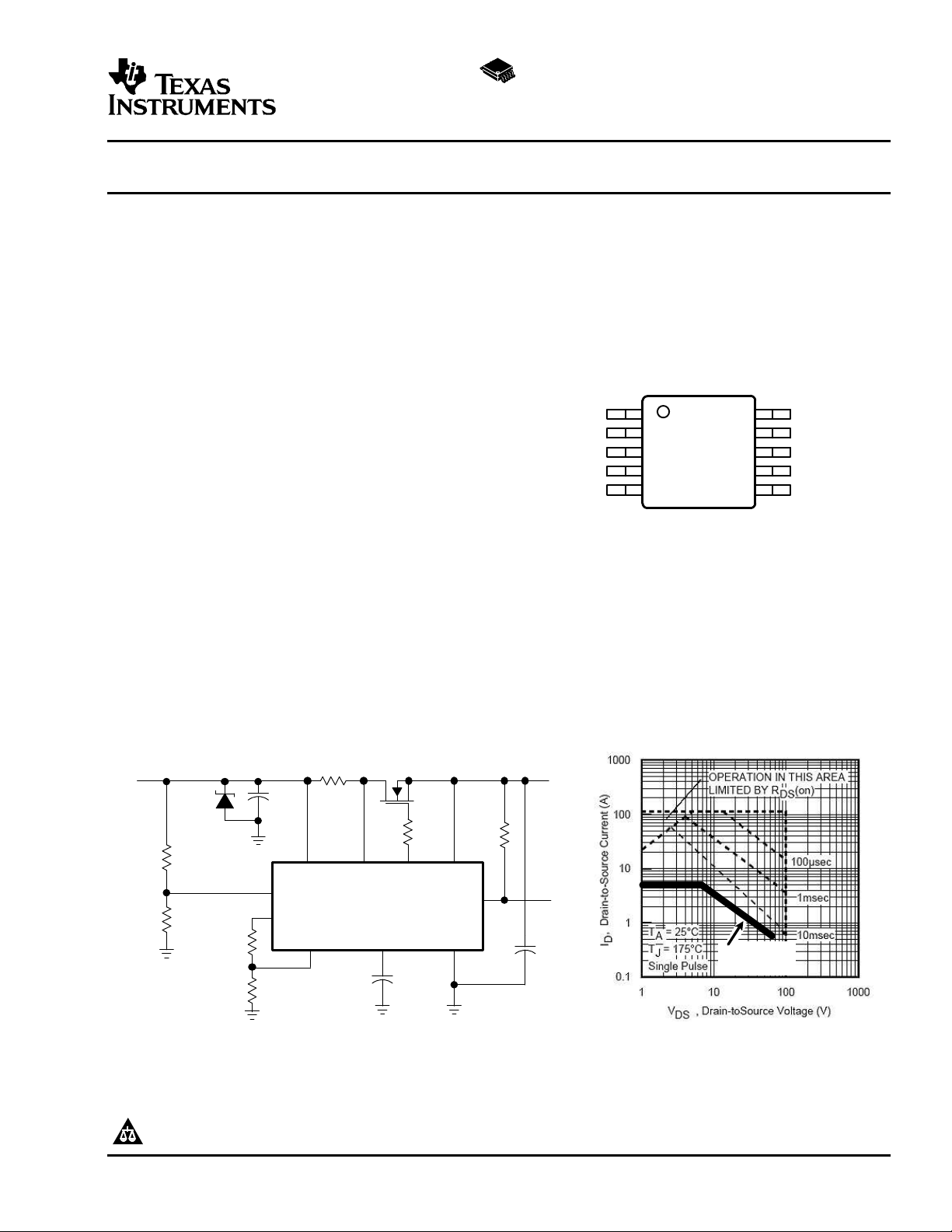
D1
SMAJ60A
C1
0.1 µF
R
S
0.01 Ω
M1
IRF540NS
R6
470 kΩ
R5
10 Ω
R3
41.2 kΩ
R4
8.25 kΩ
C
T
0.1 µF
C
O
220 µF
R1
324 kΩ
R2
13.3 kΩ
VI = 48 Vdc
VO at 4 A
Power Good
TPS2490/91
I
LIM
= 5 A,
VON/V
OFF
= 34.2 V/31.7 V,
P
LIM
= 34 W,
Timeout = 16 mS
Programmed
SOA, 16mS
POSITIVE HIGH-VOLTAGE POWER-LIMITING HOTSWAP CONTROLLER
FEATURES APPLICATIONS
• Programmable Power Limiting and Current
Limiting for Complete SOA Protection
• Wide Operating Range: +9 V to +80 V
• Latched Operation (TPS2490) and Automatic
Retry (TPS2491)
• High-side Drive for Low-R
DS(on)
External
N-channel MOSFET
• Programmable Fault Timer to Protect the
MOSFET and Eliminate Nuisance Shutdowns
• Power Good Open-Drain Output for Downstream DC/DC Coordination
• Enable can be used as a Programmable
Undervoltage Lockout or Logic Control
• Small, Space-saving 10-pin MSOP Package
• Server Backplanes
• Storage Area Networks (SAN)
• Medical Systems
• Plug-in Modules
• Base Stations
TPS2490
TPS2491
SLVS503–NOVEMBER 2003
DESCRIPTION
The TPS2490 and TPS2491 are easy-to-use, positive high voltage, 10-pin Hot Swap Power Manager™ devices
that safely drive an external N-channel MOSFET switch. The power limit and current limit (both are adjustable
and independent of each other) ensure that the external MOSFET operates inside a selected safe operating area
(SOA) under the harshest operating conditions. Applications include inrush current limiting, electronic circuit
breaker protection, controlled load turn-on, interfacing to down-stream dc-to-dc converters, and power feed
protection. These devices are available in a small, space-saving 10-pin MSOP package and significantly reduce
the number of external devices, saving precious board space. The TPS2490/91 is supported by application
notes, an evaluation module, and a design tool.
Typical Application and Corresponding SOA
Hot Swap Power Manager is a trademark of Texas Instruments.
PRODUCTION DATA information is current as of publication date.
Products conform to specifications per the terms of the Texas
Instruments standard warranty. Production processing does not
necessarily include testing of all parameters.
Please be aware that an important notice concerning availability, standard warranty, and use in critical applications of Texas
Instruments semiconductor products and disclaimers thereto appears at the end of this data sheet.
Copyright © 2002–2003, Texas Instruments Incorporated
www.ti.com
TPS2490
TPS2491
SLVS503–NOVEMBER 2003
This integrated circuit can be damaged by ESD. Texas Instruments recommends that all integrated circuits be handled with
appropriate precautions. Failure to observe proper handling and installation procedures can cause damage.
ESD damage can range from subtle performance degradation to complete device failure. Precision integrated circuits may be more
susceptible to damage because very small parametric changes could cause the device not to meet its published specifications.
ORDERING INFORMATION
TA FUNCTION PACKAGE PART NUMBER
-40°C to 85°C
(1) Add an R suffix to the device type for tape and reel packaging.
Latched VSSOP-10 TPS2490DGS BIY
Retry (MSOP) TPS2491DGS BIX
(1)
SYMBOL
ABSOLUTE MAXIMUM RATINGS
(1)
over operating free-air temperature range (unless otherwise noted)
UNIT
Input voltage range, VCC, SENSE, EN, OUT -0.3 to 100 V
Output voltage range, GATE, PG -0.3 to 100 V
Input voltage range, PROG -0.3 to 6 V
Output voltage range, TIMER, VREF -0.3 to 6 V
Sink current, PG 10 mA
Source current, VREF 0 to 2 mA
Sink Current, PROG 2 mA
ESD - human body model 2 kV
ESD - charged device model 500 V
Maximum junction temperature, T
Storage temperature, T
Lead temperature 1.6 mm (1/16 inch) from case for 10 seconds 260 °C
(1) Stresses beyond those listed under "absolute maximum ratings" may cause permanent damage to the device. These are stress ratings
only and functional operation of the device at these or any other conditions beyond those indicated under "recommended operating
conditions" is not implied. Exposure to absolute-maximum-rated conditions for extended periods may affect device reliability
ST
J
150 °C
–65 to 150 °C
RECOMMENDED OPERATING CONDITIONS
MIN NOM MAX UNIT
V
V
I
VREF
T
T
VCC
PROG
J
A
Input voltage range 9 80 V
Input voltage range 0 4 V
Operating current range (sourcing), V
Operating junction temperature -40 125 °C
Operating free-air temperature -40 85 °C
REF
0 1 mA
DISSIPATION RATING TABLE
PACKAGE TA<25°C DERATING FACTOR TA= 70°C TA= 85°C
POWER RATING ABOVE TA= 25°C POWER RATING POWER RATING
mW (mW/°C) (mW) (mW)
VSSOP-10 (MSOP) 376 3.76 207 150
2
www.ti.com
TPS2490
TPS2491
SLVS503–NOVEMBER 2003
ELECTRICAL CHARACTERISTICS
unless otherwise noted, minimum and maximum limits apply across the recommended operating junction temperature and
voltage range, V
all outputs unloaded; positive currents are into pins.
SUPPLY CURRENT (VCC)
Enabled VEN= Hi, V
Disabled VEN= Lo, V
CURRENT SENSE INPUT (SENSE)
I
SENSE
REFERENCE VOLTAGE OUTPUT (VREF)
V
REF
POWER LIMITING INPUT (PROG)
I
PROG
R
PROG
POWER LIMITING AND CURRENT LIMITING (SENSE)
V
CL
V
SENSE
t
F_TRIP
TIMER OPERATION (TIMER)
D
RETRY
GATE DRIVE OUTPUT (GATE)
I
GATE
t
D_ON
t
D_OFF
POWER GOOD OUTPUT (PG)
V
PG_L
V
PGTL
Input bias current V
Reference voltage 0 < I
Input bias current, device enabled, sourcing or
sinking
Pulldown resistance, device disabled I
Current sense threshold V
power limiting trip V
Current sense threshold V
power limiting trip
Large overload response time to GATE low
Charge current (sourcing)
Discharge current (sinking)
TIMER upper threshold voltage 3.9 4 4.1 V
TIMER lower reset threshold voltage TPS2491 only 0.96 1.0 1.04 V
Fault retry duty cycle TPS2491 only 0.5% 0.75% 1.0%
GATE sourcing current 15 22 35 µA
GATE sinking current
GATE output voltage, V
Propagation delay: EN going true to GATE VEN= 0 → 2.5 V, 50% of VENto 50% of
output high
Propagation delay: EN going false (0 V) to
GATE output low
Propagation delay: TIMER expires to GATE
output low
Low voltage (sinking)
PG threshold voltage, V
open drain
= 0 V, and all outputs unloaded; typical specifications are at TJ= 25°C, V
TIMER
VCC
= 48 V, V
TIMER
= 0 V, and
PARAMETER TEST CONDITIONS MIN TYP MAX UNIT
= V
SENSE
SENSE
= V
SENSE
VREF
0 < V
PROG
= 200 µA, VEN= 0 V 375 600 Ω
PROG
(VCC-SENSE)
(VCC-sense)
with V
without V
(1)
PROG
PROG
PROG
V
PROG
V
(VCC-SENSE)
C
(GATE-OUT)
V
TIMER
V
TIMER
V
TIMER
V
TIMER
V
SENSE
VEN= Hi
VEN= Lo, V
VEN= Hi, V
V
(VCC-SENSE)
(GATE-OUT)
(1)
V
GATE
, V
, V
VCC
< 1 mA 3.9 4 4.1 V
< 4 V, VEN= 48 V 5 µA
= 2.4 V, V
= 0.9 V, V
= 4 V, V
SENSE
= 4 V, V
OUT
: 0 → 200 mV, 1.2 µS
= 2 nF, V
= 0 V 15.0 25.0 34.0 µA
= 0 V, TJ= 25°C 20.0 25.0 30.0 µA
= 5 V 1.50 2.5 3.70 µA
= 5 V, TJ= 25°C 2.10 2.5 3.10 µA
= V
, V
VCC
= V
GATE
= V
GATE
≥ 200 mV
= V
OUT
VCC
= V
OUT
VCC
= V
= V
VCC
= V
OUT
= 0 V or
OUT
= 30 V, V
OUT
= V
= V
SENSE
(GATE-OUT)
(GATE-OUT)
VCC
, 75 125 250 mA
VCC
, R
(GATE-OUT)
= 0 90 250 µA
OUT
VCC
= 48 V
VCC
OUT
,
= 1 V
= 7 V,
= 1 MΩ
450 1000 µA
7.5 20 µA
17 25 33 mV
45 50 55 mV
1.8 2.4 2.8 mA
12 16 V
25 40 µS
VEN= 2.5 V → 0, 50% of VENto 50% of
V
, V
= V
(1)
(1)
GATE
R
(GATE-OUT)
V
TIMER
V
TIMER
R
(GATE-OUT)
OUT
= 1 MΩ, t
: 0 → 5 V, t
to 50% of V
, 0.5 1 µS
VCC
= 1 MΩ,
< 0.1 µS
FALL
< 0.1 µS, 50% of
RISE
, V
GATE
OUT
= V
, 0.8 1 µS
VCC
IPG= 2 mA 0.1 0.25 V
IPG= 4 mA 0.25 0.5 V
rising, PG goes
OUT
V
SENSE
= V
, measure V
VCC
(VCC-OUT)
0.8 1.25 1.7 V
(1) Not tested in production.
3
www.ti.com
TPS2490
TPS2491
SLVS503–NOVEMBER 2003
ELECTRICAL CHARACTERISTICS (continued)
unless otherwise noted, minimum and maximum limits apply across the recommended operating junction temperature and
voltage range, V
all outputs unloaded; positive currents are into pins.
VPGTH V
∆V
PGT
t
DPG
OUTPUT VOLTAGE FEEDBACK INPUT (OUT)
I
OUT
ENABLE INPUT (EN)
V
EN_H
V
EN_L
INPUT SUPPLY UVLO (VCC)
PG threshold voltage, V
low
PG threshold hysteresis voltage, V
PG deglitch delay, detection to output, rising
and falling edges
Leakage current, PG false, open drain 10 µA
Bias current
Threshold, VENgoing high 1.32 1.35 1.38 V
Threshold, VENgoing low 1.22 1.25 1.28 V
VENhysteresis
Leakage current VEN= 48 V 1 µA
V
VCC
V
VCC
Hysteresis
= 0 V, and all outputs unloaded; typical specifications are at TJ= 25°C, V
TIMER
VCC
= 48 V, V
TIMER
= 0 V, and
PARAMETER TEST CONDITIONS MIN TYP MAX UNIT
falling, PG goes
OUT
(SENSE-OUT)VSENSE
(2)
(2)
= V
SENSE
V
SENSE
V
= V
OUT
V
= GND, VEN= Lo, sourcing 18 40 µA
OUT
, measure V
VCC
= V
VCC
= V
VCC
, VEN= Hi, sinking 8 20 µA
VCC
(VCC-OUT)
2.2 2.7 3.2 V
1.4 V
5 9 15 ms
100 mV
turn on Rising 8.4 8.8 V
turn off Falling 7.5 8.3 V
(2)
75 mV
(2) Not tested in production.
4
www.ti.com
200
250
300
350
400
450
500
550
600
9 19 29 39 49 59 69 79
TJ = −40C
TJ = 25C
TJ = 125C
I
VCC
− Supply Current −
VCC − Supply Voltage − V
A
45
46
47
48
49
50
51
52
53
54
55
9 19 29 39 49 59 69 79
TJ = −40C
TJ = 25C
TJ = 125C
VCC − Supply Voltage − V
− Current Limit Trip − mV
V
(
VCC − Sense)
2
2.1
2.2
2.3
2.4
2.5
2.6
9 19 29 39 49 59 69 79
TJ = −40C
TJ = 25C
TJ = 125C
− Gate Pullup Current (EN = OV) − mA
I
Gate
VCC − Supply Voltage − V
15
17
19
21
23
25
27
29
31
33
35
9 19 29 39 49 59 69 79
TJ = −40C
TJ = 25C
TJ = 125C
VCC − Supply Voltage − V
− Gate Pullup Current −
Gate
A
I
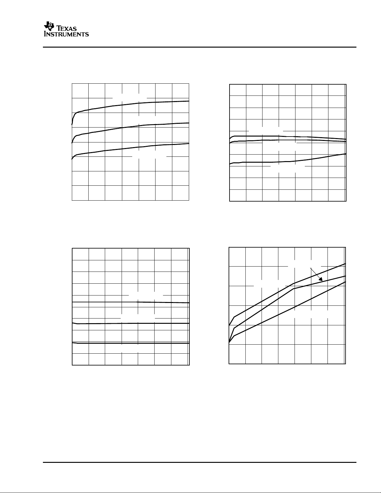
TYPICAL CHARACTERISTICS
TPS2490
TPS2491
SLVS503–NOVEMBER 2003
SUPPLY CURRENT CURRENT LIMIT TRIP
SUPPLY VOLTAGE SUPPLY VOLTAGE
GATE PULLUP CURRENT GATE PULLDOWN CURRENT(EN = 0 V)
SUPPLY VOLTAGE SUPPLY VOLTAGE
vs vs
Figure 1. Figure 2.
vs vs
Figure 3. Figure 4.
5
www.ti.com
75
95
115
135
155
175
195
215
9 19 29 39 49 59 69 79
TJ = −40C
TJ = 25C
TJ = 125C
− Gate Pulldown Current − mA
I
Gate
VCC − Supply Voltage − V
0
200
400
600
800
1000
1200
9 14 19 24 29 34 39 44 49
T − Current Limit Response Time − nS
TJ = −40C
TJ = 25C
TJ = 125C
VCC − Supply Voltage − V
18
20
22
24
26
28
30
32
9 19
29
39 49 59 69 79
− Timer Pullup Current −
TJ = −40C
TJ = 25C
TJ = 125C
I
Timer
Aµ
VCC − Supply Voltage − V
13.50
13.75
14
14.25
14.50
9 19 29 39 49 59 69 79
− Gate Output Voltage − V
TJ = −40C
TJ = 25C
TJ = 125C
VCC − Supply Voltage − V
V
Gate
TPS2490
TPS2491
SLVS503–NOVEMBER 2003
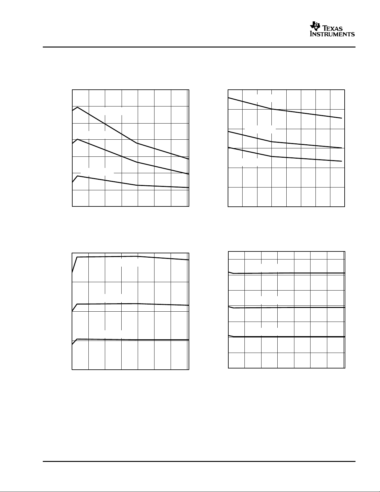
TYPICAL CHARACTERISTICS (continued)
GATE PULLDOWN CURRENT CURRENT LIMIT RESPONSE TIME
SUPPLY VOLTAGE SUPPLY VOLTAGE
(EN = 4 V, V(vcc – sense) = 200 mV) (EN = 4 V, V(vcc – sense) = 200 mV)
GATE OUTPUT VOLTAGE TIMER PULLUP CURRENT
SUPPLY VOLTAGE SUPPLY VOLTAGE
vs vs
Figure 5. Figure 6.
vs vs
6
Figure 7. Figure 8.
www.ti.com
9.60
9.65
9.70
9.75
9.80
9 19 29 39 49 59 69 79
TJ = −40C
TJ = 125C
TJ = 25C
− Charge/Discharge Ratio
I
Timer
VCC − Supply Voltage − V
1.245
1.246
1.247
1.248
1.249
1.250
1.251
1.252
1.253
1.254
1.255
9 19 29 39 49 59 69 79
− EN Threshold Voltage (Falling) − V
TJ = −40C
TJ = 125C
TJ = 25C
V
EN
VCC − Supply Voltage − V
1.345
1.346
1.347
1.348
1.349
1.350
1.351
9 19 29 39 49 59 69 79
TJ = −40C
TJ = 125C
TJ = 25C
− EN Threshold Voltage (Rising) − V
V
EN
VCC − Supply Voltage − V
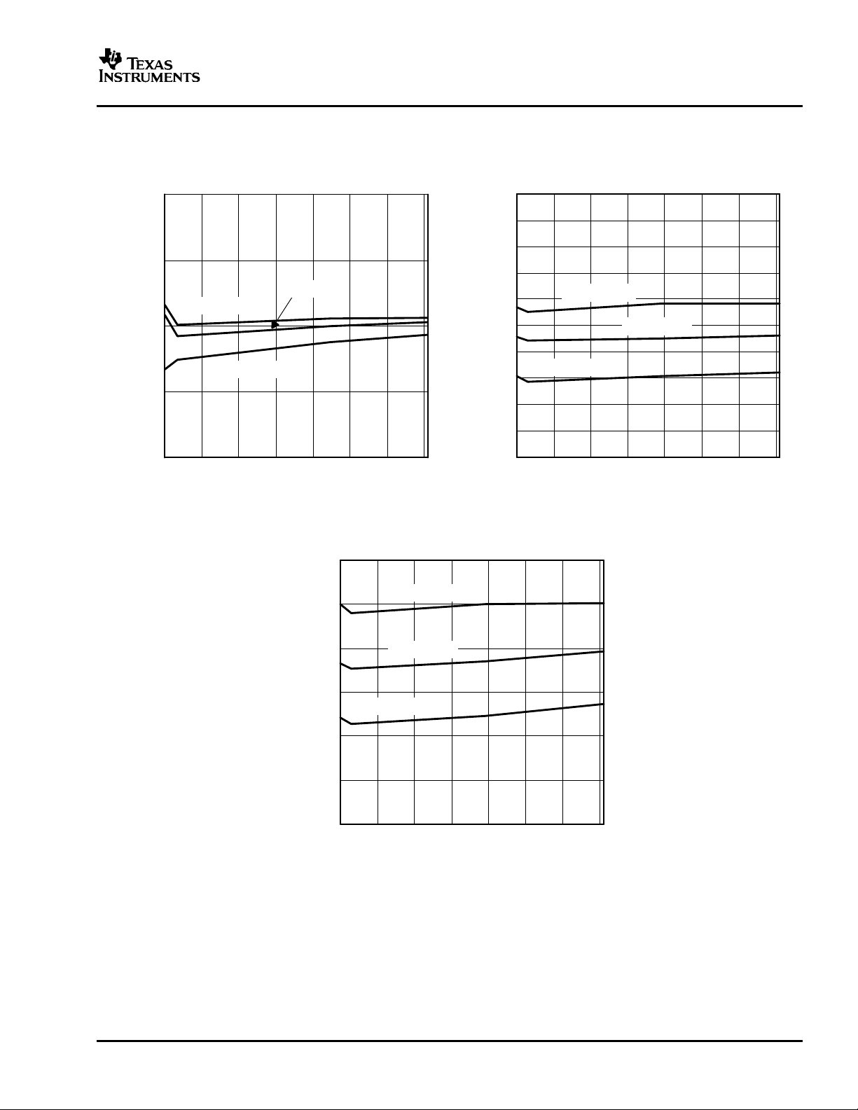
TYPICAL CHARACTERISTICS (continued)
TPS2490
TPS2491
SLVS503–NOVEMBER 2003
TIMER CHARGE/DISCHARGE RATIO EN THRESHOLD VOLTAGE (FALLING)
SUPPLY VOLTAGE AND TEMPERATURE SUPPLY VOLTAGE
vs vs
Figure 9. Figure 10.
EN THRESHOLD VOLTAGE (RISING)
vs
SUPPLY VOLTAGE
Figure 11.
7

www.ti.com
A
B
A
2B
V (DS)
Detector
Enable
Constant
Power
Engine
_
+
50 mV max
Charge
Pump
22 A
Gate Control
Amplifier
4 V
Reference
14 V
2 mA
+
−
+
−
I (D)
Detector
_
+
9 mS
Deglitch
Inrush
Complete
Power/Current
Amplifier
25 A
Fault
Logic
_
+
4 V
and
1 V
2.5 A
Timer
For Autoretry Opion with
Duty Cycle of 0.75%
_
+
_
+
UVLO
Enable
POR
8.4 V and
8.3 V
1.35 V and
1.25 V
10
VCC
3
PROG
9
SENSE
1
EN
5
GND
4
TIMER
6
PG
7
OUT
8
GATE
2
VREF
2.25 V and
1.25 V
Enable
TPS2490
TPS2491
SLVS503–NOVEMBER 2003
FUNCTIONAL BLOCK DIAGRAM
TERMINAL FUNCTIONS
I/O DESCRIPTION
TERMINAL
NAME NO.
EN 1 I Device enable
VREF 2 O Reference voltage output, used to set power threshold on PROG pin
PROG 3 I Power-limit setting input
TIMER 4 I/O Fault timing capacitor
GND 5 Ground
PG 6 O Power good reporting output, open-drain
OUT 7 I Output voltage feedback
GATE 8 O Gate output
SENSE 9 I Current-limit sense input
VCC 10 I Supply input
8

www.ti.com
I
LIM
50 mV
R
S
TPS2490
TPS2491
SLVS503–NOVEMBER 2003
DETAILED PIN DESCRIPTION
The following description relies on the typical application diagram shown on page 1, and the functional block
diagram.
VCC: This pin is associated with three functions: 1) biasing power to the integrated circuit, 2) input to power on
reset (POR) and under voltage lockout (UVLO) functions, and 3) voltage sense at one terminal of RSfor M1
current measurement. The voltage must exceed the POR (about 6 V for roughly 400µ S) and the internal UVLO
(about 8 V) before normal operation (driving the GATE) may begin. Connections to VCC should be designed to
minimize RSvoltage sensing errors and to maximize the effect of C1 and D1; place C1 at RSrather than at the IC
pin to eliminate transient sensing errors. GATE, PROG, PG, and TIMER are held low when either UVLO or POR
are active.
SENSE: Monitors the voltage at the drain of M1, and the downstream side of RSproviding the constant power
limit engine with feedback of both M1 current (ID) and voltage (VDS). Voltage is determined by the difference
between SENSE and OUT, while the current analog is the difference between VCC and SENSE. The constant
power engine uses VDSto compute the allowed IDand is clamped to 50 mV, acting like a traditional current limit
at low VDS. The current limit is set by the following equation:
Design the connections to SENSE to minimize RSvoltage sensing errors. Don’t drive SENSE to a large voltage
difference from VCC because it is internally clamped to VCC. The current limit function can be disabled by
connecting SENSE to VCC.
GATE: Provides the high side (above VCC) gate drive for M1. It is controlled by the internal gate drive amplifier,
which provides a pull-up of 22 µA from an internal charge pump and a strong pull-down to ground of 75 mA
(min). The pull-down current is a non-linear function of the amplifier overdrive; it provides small drive for small
overloads, but large overdrive for fast reaction to an output short. There is a separate pull-down of 2 mA to shut
M1 off when EN or the UVLO cause this to happen. An internal clamp protects the gate of M1 (to OUT) and
generally eliminates the need for an external clamp in almost all cases for devices with 20 V V
external Zener may be required to protect the gate of devices with V
(R5) of 10 Ω should be inserted in the gate lead if the C
of M1 > 200 pF, otherwise use 33 Ω for small
ISS
GS(MAX)
< 16 V. A small series resistance
GS(MAX)
MOSFETs.
A capacitor can be connected from GATE to ground to create a slower inrush with a constant current profile
without affecting the amplifier stability. Add a series resistor of about 1 kΩ to the gate capacitor to maintain the
gate clamping and current limit response time.
OUT: This input pin is used by the constant power engine and the PG comparator to measure VDSof M1 as
V
(VCC–SENSE).
Internal protection circuits leak a small current from this pin when it is low. If the load circuit can
drive OUT below ground, connect a clamp (or freewheel) diode such as an S1B from OUT (cathode) to GND
(anode).
EN: The GATE driver is enabled if the positive threshold is exceeded and the internal POR and UVLO thresholds
have been satisfied. EN can be used as a logic control input, an analog input voltage monitor as illustrated by
R1/R2 in the typical application circuit on page 1, or it can be tied to VCC to always enable the TPS2490/91. The
hysteresis associated with the internal comparator makes this a stable method of detecting a low input condition
and shutting the downstream circuits off. A TPS2490 that has latched off can be reset by cycling EN below its
negative threshold and back high.
VREF: Provides a 4.0-V reference voltage for use in conjunction with R3/R4 of the typical application circuit to
set the voltage on the PROG pin. The reference voltage is available once the internal POR and UVLO thresholds
have been met. It is not designed as a supply voltage for other circuitry, therefore ensure that no more than 1 mA
is drawn. Bypass capacitance is not required, but if a special application requires one, less than 1000 pF can be
placed on this pin.
PROG: The voltage applied to this pin (0–4 V) programs the power limit used by the constant power engine.
Normally, a resistor divider R3/R4 is connected from VREF to PROG to set the power limit according to the
following equation:
ratings; an
9

www.ti.com
V
PROG
P
LIM
10 I
LIM
P
LIM
T
J(MAX)
T
S(MAX)
R
JC(MAX)
TPS2490
TPS2491
SLVS503–NOVEMBER 2003
where P
is the desired power limit of M1 and I
LIM
is the current limit setpoint (see SENSE). P
LIM
is determined
LIM
by the desired thermal stress on M1:
where T
is the maximum desired transient junction temperature of M1 and T
J(MAX)
is the maximum case
S(MAX)
temperature prior to a start or restart.
V
is used in conjunction with VDSto compute the (scaled) current, I
PROG
I
D_ALLOWED
I
D_ALLOWED
regulated to maintain the ID= I
is compared by the gate amplifier to the actual ID, and used to generate a gate drive. If ID<
, the amplifier turns the gate of M1 full on because there is no overload condition; otherwise GATE is
D_ALLOWED
relationship.
D_ALLOWED
, by the constant power engine.
A capacitor may be tied from PROG to ground to alter the natural constant power inrush current shape. If
properly designed, the effect is to cause the leading step of current in Figure 12 to look like a ramp.
PROG is internally pulled to ground whenever EN, POR, or UVLO are not satisfied or the TPS2490 is latched off.
This feature serves to discharge any capacitance connected to the pin. Do not apply voltages greater than 4 V to
PROG. If the constant power limit is not used, PROG should be tied to VREF through a 47-kΩ resistor.
TIMER: An integrating capacitor, CT, connected to the TIMER pin provides a timing function that controls the
fault-time for both versions and the restart interval for the TPS2491. The timer charges at 25 µA whenever the
TPS2490/91 is in power limit or current limit and discharges at 2.5 µA otherwise. The charge-to-discharge current
ratio is constant with temperature even though there is a positive temperature coefficient to both. If TIMER
reaches 4 V, the TPS2490 pulls GATE to ground, latch off, and discharge CT. The TPS2491 pulls GATE to
ground and attempt a restart (re-enable GATE) after a timing sequence consisting of discharging CTdown to 1 V
followed by 15 more charge and discharge cycles. The TPS2490 can be reset by either cycling the EN pin or the
UVLO (e.g. power cycling). TIMER discharges when EN is low or UVLO or POR are active. The TIMER pin
should be tied to ground if this feature is not used.
PG: This open-drain output is intended to interface to downstream dc/dc converters or monitoring circuits. PG
goes open-drain (high voltage with a pull-up) after VDSof M1 has fallen to about 1.25 V and a 9 ms deglitch time
period has elapsed. PG is false (low or low resistance to ground) whenever EN is false, VDSof M1 is above
2.5 V, or UVLO is active. PG can also be viewed as having an input and output voltage monitor function. The
9-ms deglitch circuit operates to filter short events that could cause PG to go inactive (low) such as a momentary
overload or input voltage step. VPGvoltage can be greater than V
because it’s ESD protection is only with
VCC
respect to ground.
GND: This pin is connected to system ground.
10

www.ti.com
VCC CH1VCC 10 V/div
Timer 1 V/div
IIN 1 A/div
PG
10 V/div
OUT
10 V/div
TPS2490
TPS2491
SLVS503–NOVEMBER 2003
APPLICATION INFORMATION
BASIC OPERATION
The TPS2490/91 provides all the features needed for a positive hotswap controller. These features include: 1)
under-voltage lockout; 2) adjustable (system-level) enable; 3) turn-on inrush limit; 4) high-side gate drive for an
external N-channel MOSFET; 5) MOSFET protection (power limit and current limit); 6) adjustable overload
timeout—also called an electronic circuit breaker; 7) charge-complete indicator for downstream converter
coordination; and 8) an optional automatic restart mode. The TPS2490/91 features superior power-limiting
MOSFET protection that allows independent control of current limit (to set maximum full-load current), power limit
(to control junction temperature rise), and overload time (to control case temperature rise).
The typical application circuit, and oscilloscope plots of Figures 12–16 demonstrate many of the functions
described above.
Board Plug-In (Figure 12)
Only the bypass capacitor charge current and small bias currents are evident when a board is first plugged in.
The TPS2490/91 is held inactive, and GATE, PROG, TIMER, and PG are held low for less than 1 ms while
internal voltages stabilize. A startup cycle is ready to take place after the stabilization.
GATE, PROG, TIMER, and PG are released after stabilization in this example because both the internal UVLO
threshold and the external EN (enable) thresholds have been exceeded. The part begins sourcing current from
the GATE pin and M1 begins to turn on while the voltage across it, V
V
(VCC–SENSE)
, are monitored. Current initially rises to the value which satisfies the power limit engine (P
since the output capacitor was discharged.
(SENSE–OUT)
, and current through it,
÷ V
LIM
VCC
)
TIMER and PG Operation (Figure 12)
The TIMER pin charges CTas long as limiting action continues, and discharges at a 1/10 charge rate when
limiting stops. If the voltage on CTreaches 4 V before the output is charged, M1 is turned off and either a
latch-off or restart cycle commences, depending on the part type. The open-drain PG output provides a
deglitched end-of-charge indication which is based on the voltage across M1. PG is useful for preventing a
downstream dc/dc converter from starting while COis still charging. PG goes active (open drain) about 9 ms after
COis charged. This delay allows M1 to fully turn on and any transients in the power circuits to end before the
converter starts up. The resistor pull-up shown on pin PG in the typical application diagram only demonstrates
operation; the actual connection to the converter depends on the application. Timing can appear to terminate
early in some designs if operation transitions out of the power limit mode into a gate charge limited mode at low
VDSvalues.
Figure 12. Basic Board Insertion
11

www.ti.com
VCC − OUT
10 V/div
VOUT 10 V/div
I
IN
1 A/div
FET PWR 10 W/div
M1 Power Measured 29.6 W,
Calculated 34.4 W
TPS2490
TPS2491
SLVS503–NOVEMBER 2003
APPLICATION INFORMATION (continued)
Action of the Constant Power Engine (Figure 13)
The calculated power dissipated in M1, VDS× ID, is computed under the same startup conditions as Figure 12.
The current of M1, labeled IIN, initially rises to the value that satisfies the constant power engine; in this case it is
34 W ÷ 48 V = 0.7 A. The 34 W value is programmed into the engine by setting the PROG voltage using the
equation given in the PROG pin description. VDSof M1, which is calculated as V(
VCC–OUT
thus allowing the M1 drain current to increase. This is the result of the internal constant power engine adjusting
the current limit reference to the GATE amplifier as COcharges and VDSfalls. The calculated device power in
Figure 13, labeled FET PWR, is seen to be flat-topped and constant within the limitations of circuit tolerance and
acquisition noise. A fixed current limit is implemented by clamping the constant power engine’s output to 50 mV
when VDSis low. This protection technique can be viewed as a specialized form of foldback limiting; the benefit
over linear foldback is that it yields the maximum output current from a device over the full range of VDSand still
protects the device.
) , falls as COcharges,
Figure 13. Computation of M1 Stress During Startup
Response to a Hard Output Short (Figure 14 and Figure 15)
Figure 14 shows the short circuit response over the full time-out period that begins when the output voltage falls
and ends when M1 is turned off. M1 current is actively controlled by the power limiting engine and gate amplifier
circuit while the TIMER pin charges CTto the 4 V threshold that causes M1 to be turned off. The TPS2490
latches off after the threshold is reached until either the input voltage drops below the UVLO threshold or EN
cycles through the false (low) state. The TPS2491 goes through a timing sequence before attempting a restart.
12

www.ti.com
TIMER
1 V/div
I
IN
5 A/div
GATE 10 V/div
OUT 10 V/div
GATE 10 V/div
VCC 10 V/div
OUT 10 V/div
I
IN
5A/div
TPS2490
TPS2491
SLVS503–NOVEMBER 2003
APPLICATION INFORMATION (continued)
Figure 14. Current Limit Overview
The TPS2490/91 responds rapidly to the short circuit as seen in Figure 15. The falling OUT voltage is the result
of M1 and COcurrents through the short’s impedance at this time scale. The internal GATE clamp causes the
GATE voltage to follow the output voltage down and subsequently limits the negative VDSto 1–2 V. The rapidly
rising fault current overdrives the GATE amplifier causing it to overshoot and rapidly turn M1 off by sinking
current to ground. M1 slowly turns back on as the GATE amplifier recovers; M1 then settles to an equilibrium
operating point determined by the power limiting circuit.
Figure 15. Current Limit Onset
Minimal input voltage overshoot appears in Figure 15 because a local 100-µF bypass capacitor and very short
input leads were used. The input voltage would overshoot as the input current abruptly drops in a typical
application due to the stored energy in the input distribution’s inductance. The exact waveforms seen in an
application depend upon many factors including parasitics of the voltage distribution, circuit layout, and the short
itself.
13

www.ti.com
GATE 10 V/div
OUT 10 V/div
TIMER 1 V/div
I
IN
.5 A/div
R
S
0.05
1.2 I
MAX
TPS2490
TPS2491
SLVS503–NOVEMBER 2003
APPLICATION INFORMATION (continued)
Automatic Restart (Figure 16)
The TPS2491 automatically initiates a restart after a fault has caused it to turn off M1. Internal control circuits use
CTto count 16 cycles before re-enabling M1. This sequence continues to repeat if the fault persists. The TIMER
has a 1:10 charge-to-discharge current ratio, and uses a 1-V lower threshold. The fault-retry duty cycle
specification quantifies this behavior. This small duty cycle often reduces the average short-circuit power
dissipation to levels associated with normal operation and eliminates special thermal considerations for surviving
a prolonged output short.
DESIGN PROCEDURE
This design procedure seeks to control the junction temperature of M1 under both static and transient conditions
by selecting the device’s package, cooling, R
procedure assumes that a unit running at full load and maximum ambient temperature experiences a brief input
power interruption sufficient to discharge CO, but short enough to keep M1 from cooling. A full COrecharge then
takes place. Adjust this procedure to fit your application and design criteria.
This procedure assumes that COis the only load during inrush. Only simple first-order thermal models, natural
convection and a large PCB pad for M1 are assumed. The assumptions build generous safety margins into the
design to allow for the inherent inaccuracies of the models and variations of real-world conditions.
Other tools and applications information are available on the TI website that supplement the following procedure.
STEP 1. Choose R
Given the maximum operating current, I
This equation allows for minimum current limit, a sense resistor tolerance of 5%, and 5% margin. Round the
result down to the nearest available standard value.
STEP 2. Choose M1
First select a VDSrating that allows for the maximum input voltage and transients. Next select an operating
R
R
curve from which values at other temperatures can be derived. Compute the maximum allowable on-resistance,
R
Figure 16. TPS2491 Restart Cycle Timing
, current limit, fault timeout, and power limit. The following
DSON
S
, compute the current sense resistance, RS.
MAX
, package, and cooling to control operating temperature. The following equation computes the value of
DSON
DSON(MAX)
DSon(MAX)
at a junction temperature of T
, using the equation:
. Most manufacturers list R
J(MAX)
DSON(MAX)
at 25°C and provide a derating
14

www.ti.com
R
DSON(MAX)
T
J(MAX)
T
A(MAX)
R
JA
I
2
MAX
P
LIM
0.7
T
J(MAX)2
I
2
MAX
R
DSON
R
CA
T
A(MAX)
R
JC
V
PROG
P
LIM
10 I
LIM
where I
LIM
0.05
R
S
R4
R3 R4
V
PROG
V
REF
CO P
LIM
2 I
2
LIM
CO V
2
VCC(MAX)
2 P
LIM
if P
LIM
I
LIMVVCC(MAX)
t
ON
CO V
VCC(MAX)
I
LIM
if P
LIM
I
LIMVVCC(MAX)
CT 8.5 106 t
ON
1 C
OUT_TOL
C
T_TOL
V
ON
1.35 V
R2
R1R2
V
OFF
1.25 V
R2
R1R2
APPLICATION INFORMATION (continued)
TPS2490
TPS2491
SLVS503–NOVEMBER 2003
where T
maximum ambient temperature. R
style chosen and the details of heat-sinking and cooling. Note the R
STEP 3. Choose P
M1 dissipates large amounts of power during power-up or output short circuit. The power limit P
is the desired maximum steady-state junction temperature (typically 125°C), and T
J(MAX)
, R3, R4
LIM
, the junction-to-ambient thermal resistance, depends upon the package
θJA
θJC
and R
for use below.
θJA
A(MAX)
LIM
is the
of the
TPS2940/91 should be set to prevent the die temperature from exceeding a short term maximum temperature,
T
manufacturer’s rating of 175°C. An expression for calculating P
where R
temperature, and the factor of 0.7 represents the tolerance of the constant power engine. Next calculate V
. The short-term T
J(MAX)2
is M1 junction-to-case thermal resistance, R
θJC
J(MAX)2
could be set as high as 150°C while still leaving ample margin to the usual
is:
LIM
is the channel resistance at the maximum operating
DSON
PROG
and the divider resistors R3 and R4. R3 must be greater than 4 kΩ, but it is recommended that 10 kΩ or greater
be used.
STEP 4. Choose tON, C
T
The on-time, tON, set by capacitor CTmust suffice to fully charge the load capacitance COwithout triggering the
fault circuitry. Assuming that only the load capacitance draws current during startup:
Using this value of tON, CTis computed as:
where C
part, C
STEP 5. Choose The Turn On Voltage, R1 & R2
Assuming that EN is used as an analog input, the turn-on voltage, VONand turn-off voltage, V
Use caution in selecting very large values of R1 and R2 because the leakage current causes errors in the
threshold voltages.
T_TOL
OUT_TOL
and C
OUT_TOL
are the tolerances associated with each capacitor. Assuming COis a 20% tolerance
has a value of 0.2. This expression assures the worst case set of parts will always start.
are defined as:
OFF
15

www.ti.com
t
CO V
VCC
I
CHARGE
C
G
I
GATE
t
V
VCC
C
ISS
TPS2490
TPS2491
SLVS503–NOVEMBER 2003
APPLICATION INFORMATION (continued)
STEP 6. Choose R5, R6, & C1
R5 is intended to suppress high-frequency oscillations; a resistor of 10Ω will serve for most applications but if M1
has a C
require R5. R6 is required only if the PG output drives a circuit that requires it. It is recommended that the sink
current be less than 2 mA. C1 is a bypass capacitor to help with control of transient voltages, unit emissions, and
local supply noise while in the disabled state. Where acceptable, a value in the range of 0.001 µF to 0.1 µF is
recommended.
STEP 7. Choose D1
Transient voltage suppressor D1 is required in applications where there will be enough energy in the distribution
inductance to cause a voltage surge above the TPS2490/91 rated maximum. Such transients can be caused by
card insertions or shorts on the input or output of the TPS2490/91.
ALTERNATIVE INRUSH DESIGNS
Gate Capacitor (dV/dt) Control
The TPS2490/91 can be used with applications that require constant turn-on currents. The current is controlled
by a single capacitor from the GATE terminal to ground with a series resistor. M1 appears to operate as a source
follower (following the gate voltage) in this implementation. Choose a time to charge, ∆t, based on the output
capacitor, input voltage VI, and desired charge current, I
power limit feature is kept.
below 200 pF, then use 33 Ω. Applications with larger MOSFETs and very short wiring may not
ISS
CHARGE
. Select I
CHARGE
to be less than P
LIM
÷ V
VCC
if the
To select the gate capacitance:
where C
is the gate capacitance of M1, and I
ISS
is the nominal gate charge current. The TIMER capacitor
GATE
can then be selected to be much smaller as the current and power limit is not active during initial power on. A
series resistor of about 1 kΩ should be used in conjunction with CG.
PROG Inrush Control
A capacitor can be connected from the PROG pin to ground to reduce the initial current step seen in Figure 12
based on the typical application circuit on page 1. This method maintains a relatively fast turn-on time without the
drawbacks of a gate-to-ground capacitor that include increased short circuit response time and less predictable
gate clamping.
ADDITIONAL DESIGN CONSIDERATIONS
Use of PG
Use the PG pin to control and coordinate a downstream dc/dc converter. A long time delay is needed to allow C
to fully charge before the converter starts if this is not done. An undesirable latchup condition can be created
between the TPS2490 output characteristic and the dc/dc converter input characteristic if the converter starts
while COis still charging; the PG pin is one way to avoid this.
Faults and Backplane Voltage Droop
A hard short at the output of the TPS2490/91 during normal operation could result in activation of the enable or
UVLO circuit instead of the current limit if the input voltage droops sufficiently. The lower GATE drive in this
condition will cause a prolonged, larger over-current spike. This can be eliminated by filtering EN, or distributing
capacitance on the bus itself. Capacitance from adjacent plugged-in units may help with this as well.
O
16

www.ti.com
TPS2490
TPS2491
SLVS503–NOVEMBER 2003
APPLICATION INFORMATION (continued)
Output Clamp Diode
Inductive loads on the output may drive the OUT pin below GND when the circuit is unplugged or during a
current limit. The OUT pin ratings can be maintained with a small diode, such as an S1B, across TPS2490/91
OUT to GND.
Gate Clamp Diode
The TPS2490/91 has a relatively well-regulated gate voltage of 12–16 V, even with low supply voltages. A small
clamp Zener from gate to source of M1, such as a BZX84C7V5, is recommended if VGSof M1 is rated below this.
High Gate Capacitance Applications
Gate voltage overstress and abnormally large fault current spikes can be caused by large gate capacitance. An
external gate clamp Zener diode is recommended if the total gate capacitance of M1 exceeds about 4000 pF.
When gate capacitor inrush control is used, a 1-kΩ resistor in series with CGis recommended. If the series R-C
combination is used for MOSFETs with C
Output Short Circuit Measurements
Repeatable short-circuit testing results are difficult to obtain. The many details of source bypassing, input leads,
circuit layout and component selection, output shorting method, relative location of the short, and instrumentation
all contribute to obtaining different results. The actual short itself exhibits a certain degree of randomness as it
microscopically bounces and arcs. Care in configuration and methods must be used to obtain realistic results. Do
not expect to see waveforms exactly like those in the data sheet—every setup differs.
less than 3000 pF, then a Zener is not necessary.
ISS
Layout Considerations
Good layout practice places the power devices D1, RS, M1, and COso power flows in a sequential fashion, and
preferably in a straight line. A ground plane under the power and the TPS2490/91 is desirable. The TPS2490/91
should be placed close to the sense resistor and the MOSFET; a Kelvin connection is recommended to achieve
accurate current sensing across RS. A low-impedance GND connection is required because the TPS2490/91 can
momentarily sink upwards of 100 mA from the gate of M1. The GATE amplifier has high bandwidth while active,
so keep the gate trace length short. The PROG, TIMER, and EN pins have high input impedances, therefore
keep their input leads short. Oversize power traces and power device connections to assure low voltage drop
and good thermal performance.
17

PACKAGE OPTION ADDENDUM
www.ti.com
6-Dec-2006
PACKAGING INFORMATION
Orderable Device Status
(1)
Package
Type
Package
Drawing
Pins Package
Qty
Eco Plan
TPS2490DGS ACTIVE MSOP DGS 10 80 Green (RoHS &
no Sb/Br)
TPS2490DGSG4 ACTIVE MSOP DGS 10 80 Green (RoHS &
no Sb/Br)
TPS2490DGSR ACTIVE MSOP DGS 10 2500 Green (RoHS &
no Sb/Br)
TPS2490DGSRG4 ACTIVE MSOP DGS 10 2500 Green (RoHS &
no Sb/Br)
TPS2491DGS ACTIVE MSOP DGS 10 80 Green (RoHS &
no Sb/Br)
TPS2491DGSG4 ACTIVE MSOP DGS 10 80 Green (RoHS &
no Sb/Br)
TPS2491DGSR ACTIVE MSOP DGS 10 2500 Green (RoHS &
no Sb/Br)
TPS2491DGSRG4 ACTIVE MSOP DGS 10 2500 Green (RoHS &
no Sb/Br)
(1)
The marketing status values are defined as follows:
ACTIVE: Product device recommended for new designs.
LIFEBUY: TI has announced that the device will be discontinued, and a lifetime-buy period is in effect.
NRND: Not recommended for new designs. Device is in production to support existing customers, but TI does not recommend using this part in
a new design.
PREVIEW: Device has been announced but is not in production. Samples may or may not be available.
OBSOLETE: TI has discontinued the production of the device.
(2)
Lead/Ball Finish MSL Peak Temp
CU NIPDAU Level-2-260C-1 YEAR
CU NIPDAU Level-2-260C-1 YEAR
CU NIPDAU Level-2-260C-1 YEAR
CU NIPDAU Level-2-260C-1 YEAR
CU NIPDAU Level-2-260C-1 YEAR
CU NIPDAU Level-2-260C-1 YEAR
CU NIPDAU Level-2-260C-1 YEAR
CU NIPDAU Level-2-260C-1 YEAR
(3)
(2)
Eco Plan - The planned eco-friendly classification: Pb-Free (RoHS), Pb-Free (RoHS Exempt), or Green (RoHS & no Sb/Br) - please check
http://www.ti.com/productcontent for the latest availability information and additional product content details.
TBD: The Pb-Free/Green conversion plan has not been defined.
Pb-Free (RoHS): TI's terms "Lead-Free" or "Pb-Free" mean semiconductor products that are compatible with the current RoHS requirements
for all 6 substances, including the requirement that lead not exceed 0.1% by weight in homogeneous materials. Where designed to be soldered
at high temperatures, TI Pb-Free products are suitable for use in specified lead-free processes.
Pb-Free (RoHS Exempt): This component has a RoHS exemption for either 1) lead-based flip-chip solder bumps used between the die and
package, or 2) lead-based die adhesive used between the die and leadframe. The component is otherwise considered Pb-Free (RoHS
compatible) as defined above.
Green (RoHS & no Sb/Br): TI defines "Green" to mean Pb-Free (RoHS compatible), and free of Bromine (Br) and Antimony (Sb) based flame
retardants (Br or Sb do not exceed 0.1% by weight in homogeneous material)
(3)
MSL, Peak Temp. -- The Moisture Sensitivity Level rating according to the JEDEC industry standard classifications, and peak solder
temperature.
Important Information and Disclaimer:The information provided on this page represents TI's knowledge and belief as of the date that it is
provided. TI bases its knowledge and belief on information provided by third parties, and makes no representation or warranty as to the
accuracy of such information. Efforts are underway to better integrate information from third parties. TI has taken and continues to take
reasonable steps to provide representative and accurate information but may not have conducted destructive testing or chemical analysis on
incoming materials and chemicals. TI and TI suppliers consider certain information to be proprietary, and thus CAS numbers and other limited
information may not be available for release.
In no event shall TI's liability arising out of such information exceed the total purchase price of the TI part(s) at issue in this document sold by TI
to Customer on an annual basis.
Addendum-Page 1

PACKAGE MATERIALS INFORMATION
www.ti.com
30-Jun-2007
TAPE AND REEL INFORMATION
Pack Materials-Page 1

PACKAGE MATERIALS INFORMATION
www.ti.com
Device Package Pins Site Reel
Diameter
(mm)
TPS2490DGSR DGS 10 NSE 330 12 5.3 3.3 1.3 8 12 Q1
TPS2491DGSR DGS 10 NSE 330 12 5.3 3.3 1.3 8 12 Q1
Reel
Width
(mm)
A0 (mm) B0 (mm) K0 (mm) P1
(mm)W(mm)
30-Jun-2007
Pin1
Quadrant
TAPE AND REEL BOX INFORMATION
Device Package Pins Site Length (mm) Width (mm) Height (mm)
TPS2490DGSR DGS 10 NSE 370.0 355.0 75.0
TPS2491DGSR DGS 10 NSE 370.0 355.0 75.0
Pack Materials-Page 2


IMPORTANT NOTICE
Texas Instruments Incorporated and its subsidiaries (TI) reserve the right to make corrections, modifications, enhancements,
improvements, and other changes to its products and services at any time and to discontinue any product or service without notice.
Customers should obtain the latest relevant information before placing orders and should verify that such information is current and
complete. All products are sold subject to TI’s terms and conditions of sale supplied at the time of order acknowledgment.
TI warrants performance of its hardware products to the specifications applicable at the time of sale in accordance with TI’s
standard warranty. Testing and other quality control techniques are used to the extent TI deems necessary to support this
warranty. Except where mandated by government requirements, testing of all parameters of each product is not necessarily
performed.
TI assumes no liability for applications assistance or customer product design. Customers are responsible for their products and
applications using TI components. To minimize the risks associated with customer products and applications, customers should
provide adequate design and operating safeguards.
TI does not warrant or represent that any license, either express or implied, is granted under any TI patent right, copyright, mask
work right, or other TI intellectual property right relating to any combination, machine, or process in which TI products or services
are used. Information published by TI regarding third-party products or services does not constitute a license from TI to use such
products or services or a warranty or endorsement thereof. Use of such information may require a license from a third party under
the patents or other intellectual property of the third party, or a license from TI under the patents or other intellectual property of TI.
Reproduction of TI information in TI data books or data sheets is permissible only if reproduction is without alteration and is
accompanied by all associated warranties, conditions, limitations, and notices. Reproduction of this information with alteration is an
unfair and deceptive business practice. TI is not responsible or liable for such altered documentation. Information of third parties
may be subject to additional restrictions.
Resale of TI products or services with statements different from or beyond the parameters stated by TI for that product or service
voids all express and any implied warranties for the associated TI product or service and is an unfair and deceptive business
practice. TI is not responsible or liable for any such statements.
TI products are not authorized for use in safety-critical applications (such as life support) where a failure of the TI product would
reasonably be expected to cause severe personal injury or death, unless officers of the parties have executed an agreement
specifically governing such use. Buyers represent that they have all necessary expertise in the safety and regulatory ramifications
of their applications, and acknowledge and agree that they are solely responsible for all legal, regulatory and safety-related
requirements concerning their products and any use of TI products in such safety-critical applications, notwithstanding any
applications-related information or support that may be provided by TI. Further, Buyers must fully indemnify TI and its
representatives against any damages arising out of the use of TI products in such safety-critical applications.
TI products are neither designed nor intended for use in military/aerospace applications or environments unless the TI products are
specifically designated by TI as military-grade or "enhanced plastic." Only products designated by TI as military-grade meet military
specifications. Buyers acknowledge and agree that any such use of TI products which TI has not designated as military-grade is
solely at the Buyer's risk, and that they are solely responsible for compliance with all legal and regulatory requirements in
connection with such use.
TI products are neither designed nor intended for use in automotive applications or environments unless the specific TI products
are designated by TI as compliant with ISO/TS 16949 requirements. Buyers acknowledge and agree that, if they use any
non-designated products in automotive applications, TI will not be responsible for any failure to meet such requirements.
Following are URLs where you can obtain information on other Texas Instruments products and application solutions:
Products Applications
Amplifiers amplifier.ti.com Audio www.ti.com/audio
Data Converters dataconverter.ti.com Automotive www.ti.com/automotive
DSP dsp.ti.com Broadband www.ti.com/broadband
Interface interface.ti.com Digital Control www.ti.com/digitalcontrol
Logic logic.ti.com Military www.ti.com/military
Power Mgmt power.ti.com Optical Networking www.ti.com/opticalnetwork
Microcontrollers microcontroller.ti.com Security www.ti.com/security
RFID www.ti-rfid.com Telephony www.ti.com/telephony
Low Power www.ti.com/lpw Video & Imaging www.ti.com/video
Wireless
Wireless www.ti.com/wireless
Mailing Address: Texas Instruments, Post Office Box 655303, Dallas, Texas 75265
Copyright © 2007, Texas Instruments Incorporated
 Loading...