

VPWR
TPS23882
+54V
2P Port #5
0.1uF
100V
0.1uF
100V
2P Port #6
SEN6
GAT6
DRAIN6
KSENSEC
0.200:
SEN5
GAT5
DRAIN5
0.200:
VDD
+3.3V
SEN2
GAT2
DRAIN2
KSENSEA
SEN1
GAT1
DRAIN1
Note: Only four channels shown
Alt A RJ45 & XFrmr
Alt A RJ45 & XFrmr
2P Port #7
2P Port #8
Alt A RJ45 & XFrmr
Alt A RJ45 & XFrmr
SCL
INT
SDAO
SDAI
I2C Bus
2P Port #1
0.1uF
100V
0.1uF
100V
2P Port #2
0.200:
0.200:
Alt A
RJ45 & XFrmr
Alt ARJ45 & XFrmr
2P Port #3
2P Port #4
Alt ARJ45 & XFrmr
Alt ARJ45 & XFrmr
GND
www.ti.com
SLVSF21D – AUGUST 2019 – REVISED AUGUST 2020
SLVSF21D – AUGUST 2019 – REVISED AUGUST 2020
TPS23882 Type-3 2-Pair 8-Channel PoE 2 PSE Controller with SRAM and 200 mΩ
R
SENSE
TPS23882
TPS23882
1 Features
• IEEE 802.3bt PSE solution for PoE 2 Type-3 2-Pair
Power Over Ethernet applications
• Compatible with TI's FirmPSE system firmware
• SRAM Programmable memory
• Programmable power limiting accuracy ±3%
• 200-mΩ Current sense resistor
• Legacy PD capacitance measurement
• Selectable 2-pair port power allocations
– 4 W, 7 W, 15.4 W, or 30 W
• Dedicated 14-bit integrating current ADC per port
– Noise immune MPS for DC disconnect
– 2% Current sensing accuracy
• 1- or 3-Bit fast port shutdown input
• Auto-class discovery and power measurement
• Never Fooled 4-Point detection
• Inrush and operational foldback protection
• 425-mA and 1.25-A Selectable current limits
• Port re-mapping
• 8-Bit or 16-bit I2C communication
• Flexible processor controlled operating modes
– Auto, semi auto and manual / diagnostic
• Per Port voltage monitoring and telemetry
• –40°C to +125°C Temperature operation
2 Applications
• Video recorder (NVR, DVR, and so forth)
• Small business switch
• Campus and branch switches
3 Description
The TPS23882 is an 8-channel power sourcing
equipment (PSE) controller engineered to insert
power onto Ethernet cables in accordance with the
IEEE 802.3bt standard. The PSE controller can detect
powered devices (PDs) that have a valid signature,
complete mutual identification, and apply power.
The TPS23882 improves on the TPS2388 with
reduced current sense resistors, SRAM
programmability, programmable power limiting,
capacitance measurement, and compatibility with TI's
FirmPSE system firmware (see Device Comparison
Table).
Programmable SRAM enables in-field firmware
upgradability over I2C to ensure IEEE compliance and
interoperability with the latest PoE enabled devices.
Dedicated per port ADCs provide continuous port
current monitoring and the ability to perform parallel
classification measurements for faster port turn on
times. A 1.25-A port current limit and adjustable
power limiting allows for the support of non-standard
applications above 60-W sourced. The 200-mΩ
current sense resistor and external FET architecture
allow designs to balance size, efficiency, thermal and
solution cost requirements.
Port remapping and pin-to-pin compatibility with the
TPS2388, TPS23880, and TPS23881 devices eases
migration from previous generation PSE designs and
enables interchangeable 2-layer PCB designs to
accommodate different system PoE power
configurations.
Device Information
PART NUMBER PACKAGE BODY SIZE (NOM)
TPS23882 VQFN (56) 8.00 mm × 8.00 mm
(1)
An IMPORTANT NOTICE at the end of this data sheet addresses availability, warranty, changes, use in safety-critical applications,
Copyright © 2020 Texas Instruments Incorporated
intellectual property matters and other important disclaimers. PRODUCTION DATA.
(1) For all available packages, see the orderable addendum at
the end of the data sheet.
Simplified Schematic
Product Folder Links: TPS23882
Submit Document Feedback
1

TPS23882
SLVSF21D – AUGUST 2019 – REVISED AUGUST 2020
Table of Contents
1 Features............................................................................1
2 Applications..................................................................... 1
3 Description.......................................................................1
4 Revision History.............................................................. 2
5 Device Comparison Table............................................... 3
6 Pin Configuration and Functions...................................4
6.1 Detailed Pin Description..............................................5
7 Specifications.................................................................. 7
7.1 Absolute Maximum Ratings........................................ 7
7.2 ESD Ratings............................................................... 7
7.3 Recommended Operating Conditions.........................7
7.4 Thermal Information....................................................7
7.5 Electrical Characteristics.............................................8
7.6 Typical Characteristics..............................................14
8 Parameter Measurement Information.......................... 19
8.1 Timing Diagrams.......................................................19
9 Detailed Description......................................................21
9.1 Overview................................................................... 21
9.2 Functional Block Diagram......................................... 25
9.3 Feature Description...................................................26
9.4 Device Functional Modes..........................................28
www.ti.com
2
9.5 I
C Programming...................................................... 29
9.6 Register Maps...........................................................32
10 Application and Implementation.............................. 102
10.1 Application Information......................................... 102
10.2 Typical Application................................................ 104
11 Power Supply Recommendations............................110
11.1 VDD.......................................................................110
11.2 VPWR....................................................................110
12 Layout......................................................................... 111
12.1 Layout Guidelines..................................................111
12.2 Layout Example.................................................... 112
13 Device and Documentation Support........................113
13.1 Documentation Support........................................ 113
13.2 Receiving Notification of Documentation Updates 113
13.3 Support Resources............................................... 113
13.4 Trademarks........................................................... 113
13.5 Electrostatic Discharge Caution............................ 113
13.6 Glossary................................................................ 113
14 Mechanical, Packaging, and Orderable
Information.................................................................. 113
4 Revision History
NOTE: Page numbers for previous revisions may differ from page numbers in the current version.
Changes from Revision C (May 2020) to Revision D (August 2020) Page
• Updated the numbering format for tables, figures and cross-references throughout the document...................1
Changes from Revision B (October 2019) to Revision C (May 2020) Page
• Deleted Autonomous operation description throughout data sheet for clarification ...........................................4
• Changed Gate 1-8 MAX voltage from 12 to 13 V in the Absolute Maximum Ratings table ...............................7
Changes from Revision A (September 2019) to Revision B (December 2019) Page
• Fixed typo in device number on first page ......................................................................................................... 1
Changes from Revision * (August 2019) to Revision A (September 2019) Page
• Changed from Advance Information to Production Data ................................................................................... 1
• First Public Release............................................................................................................................................1
2 Submit Document Feedback
Copyright © 2020 Texas Instruments Incorporated
Product Folder Links: TPS23882

www.ti.com
SLVSF21D – AUGUST 2019 – REVISED AUGUST 2020
5 Device Comparison Table
Table 5-1 summarizes the primary differences between the available 2-Pair PSE devices.
KEY FEATURES TPS23880 TPS23881 TPS23882
TPS23882
Compatible with TI's FirmPSE system
firmware
Pin to Pin compatible Yes Yes Yes
Number of PSE Channels 8 8 8
Supported IEEE 802.3 PSE Types
R
SENSE
2-Pair P
4-Pair P
90+ W 4-pair P
programable ranges 0.5 W to 54 W 2 W to 65 W 2 W to 65 W
CUT
programable ranges 0.5 W to 108 W 4 W to 127 W N/A
CUT
accuracy ±3.0 % ±2.5 % N/A
CUT
Channel capacitance measurement
range
ULA Packaging No Yes (TPS23881A) N/A
I2C Programmable SRAM Memory 16 kB 16 kB 16 kB
Table 5-1. 2-Pair PSE Key Feature Comparisons
KEY FEATURES TPS23861 TPS2388 TPS23881 TPS23882
Compatible with TI's FirmPSE
system firmware
Pin to Pin compatible N/A Yes Yes Yes
Number of PSE Channels 4 8 8 8
Supported IEEE 802.3 PSE
Types
R
SENSE
2-Pair P
ranges
T
MPS
programable
CUT
I
CUT
Port Current Limit (1x / 2x) 425 mA / 1060 mA 425 mA / 1060 mA 425 mA / 1250 mA 425 mA / 1250 mA
Channel capacitance
measurement range
PD Autoclass Discovery and
Power Measurement
I2C Programmable SRAM
Memory
N/A N/A Yes Yes
PoE 1
802.3at Type 1 or 2
0.255 Ω 0.255 Ω 0.200 Ω 0.200 Ω
N/A
adjustable up to 920
mA
15 ms 15 ms 3 ms 3 ms
N/A N/A 1 µF to 12 µF 1 µF to 12 µF
N/A N/A Yes Yes
N/A N/A 16 kB 16 kB
N/A Yes Yes
PoE 2
802.3bt Type 3 or 4
(2 or 4 Pair)
PoE 2
802.3bt Type 3 or 4
(2 or 4 Pair)
802.3bt Type 3 (2-Pair)
0.255 Ω 0.200 Ω 0.200 Ω
N/A 1 µF to 12 µF 1 µF to 12 µF
PoE 1
802.3at Type 1 or 2
PoE 2
802.3bt Type 3 or 4
(2 or 4 Pair)
N/A
I
adjustable up to 920
CUT
2 W to 65 W 2 W to 65 W
mA
PoE 2
PoE 2
802.3bt Type 3 (2-Pair)
Copyright © 2020 Texas Instruments Incorporated
Product Folder Links: TPS23882
Submit Document Feedback
3
8
9
10
11
12
13
14
DRAIN3
DRAIN4
GAT4
SEN4
15
16
17
18
19
20
21
NC
NC
SEN3
OSS
SDAO
56
55
54
53
52
51
50
NC
NC
TEST4
AGND
NC
SCL
A4
A3
SDAI
35
34
33
32
31
30
29
VPWR
22
23
24
NC
TEST1
TEST2
1
2
3
4
5
6
7
DRAIN1
KSENSA
DRAIN2
GAT2
SEN2
SEN1
25
TEST3
26
27
28
TEST0
NC
NC
42
41
40
39
38
37
36
A2
A1
49
48
47
46
45
44
43
INT
DGND
RESET
VDD
TEST5
GAT1
GAT3
KSENSB
DRAIN6
DRAIN5
GAT5
SEN5
SEN6
DRAIN8
KSENSD
DRAIN7
GAT7
SEN7
SEN8
GAT8
GAT6
KSENSC
Thermal Pad
TPS23882
SLVSF21D – AUGUST 2019 – REVISED AUGUST 2020
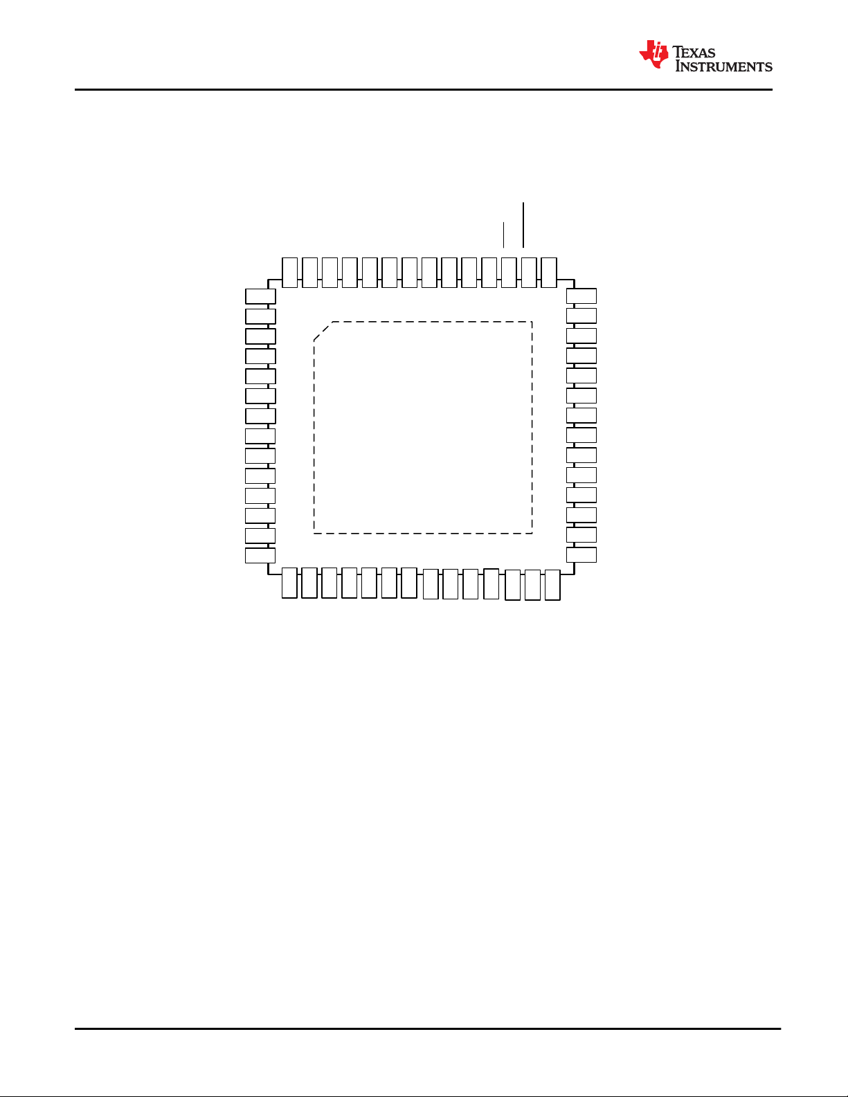
6 Pin Configuration and Functions
www.ti.com
Figure 6-1. RTQ Package With Exposed Thermal Pad 56-Pin VQFN Top View
4 Submit Document Feedback
Product Folder Links: TPS23882
Copyright © 2020 Texas Instruments Incorporated

www.ti.com
Pin Functions
SLVSF21D – AUGUST 2019 – REVISED AUGUST 2020
TPS23882
PIN
NAME NO.
A1-4 48–51 I I2C A1-A4 address lines. These pins are internally pulled up to VDD.
AGND 21 — Analog ground. Connect to GND plane and exposed thermal pad.
DGND 46 — Digital ground. Connect to GND plane and exposed thermal pad.
DRAIN1-8
GAT1-8
INT 45 O Interrupt output. This pin asserts low when a bit in the interrupt register is asserted. This output is open-drain.
KSENSA/B 4, 11 I Kelvin point connection for SEN1-4
KSENSC/D 32, 39 I Kelvin point connection for SEN5-8
NC
OSS 56 I Channel 1-8 fast shutdown. This pin is internally pulled down to DGND.
RESET 44 I Reset input. When asserted low, the TPS23882 is reset. This pin is internally pulled up to VDD.
SCL 53 I Serial clock input for I2C bus.
SDAI 54 I Serial data input for I2C bus. This pin can be connected to SDAO for non-isolated systems.
SDAO 55 O
SEN1-8
TEST0-5
Thermal pad — — The DGND and AGND terminals must be connected to the exposed thermal pad for proper operation.
VDD 43 — Digital supply. Bypass with 0.1 µF to DGND pin.
VPWR 17 — Analog 54-V positive supply. Bypass with 0.1 µF to AGND pin.
3, 5, 10, 12, 31,
33, 38, 40
1, 7, 8, 14, 29, 35,
36, 42
15, 16, 18, 19 O
22, 27, 28, 52 — No connect pin. Leave open.
2, 6, 9, 13, 30, 34,
37, 41
20, 23, 24, 25, 26,
47
I/O DESCRIPTION
I Channel 1-8 output voltage monitor.
O Channel 1-8 gate drive output.
No connect pins. These pins are internally biased at 1/3 and 2/3 of VPWR in order to control the voltage
gradient from VPWR. Leave open.
Serial data output for I2C bus. This pin can be connected to SDAI for non-isolated systems. This output is opendrain.
I Channel 1-8 current sense input.
I/O Used internally for test purposes only. Leave open.
6.1 Detailed Pin Description
The following descriptions refer to the pinout and the functional block diagram.
DRAIN1-DRAIN8: Channels 1-8 output voltage monitor and detect sense. Used to measure the port output
voltage, for port voltage monitoring, port power good detection and foldback action. Detection probe currents
also flow into this pin.
The TPS23882uses an innovative 4-point technique to provide reliable PD detection and avoids powering an
invalid load. The discovery is performed by sinking two different current levels via the DRAINn pin, while the PD
voltage is measured from VPWR to DRAINn. If prior to starting a new detection cycle the port voltage is >2.5 V,
an internal 100-kΩ resistor is connected in parallel with the port and a 400-ms detect backoff period is applied to
allow the port capacitor to be discharged before the detection cycle starts.
There is an internal resistor between each DRAINn pin and VPWR in any operating mode except during
detection or while the port is ON. If the port n is not used, DRAINn can be left floating or tied to GND.
GAT1-GAT8: Channels 1-8 gate drive outputs are used for external N-channel MOSFET gate control. At port
turn on, it is driven positive by a low current source to turn the MOSFET on. GATn is pulled low whenever any of
the input supplies are low or if an overcurrent timeout has occurred. GATn is also pulled low if the port is turned
off by use of manual shutdown inputs. Leave floating if unused.
For improved design robustness, the current foldback functions limit the power dissipation of the MOSFET
during low resistance load or short-circuit events and during the inrush period at port turn on. There is also fast
overload protection comparator for major faults like a direct short that forces the MOSFET to turn off in less than
a microsecond.
Copyright © 2020 Texas Instruments Incorporated
Product Folder Links: TPS23882
Submit Document Feedback
5

TPS23882
SLVSF21D – AUGUST 2019 – REVISED AUGUST 2020
www.ti.com
The circuit leakage paths between the GATn pin and any nearby DRAINn pin, GND or Kelvin point connection
must be minimized (< 250 nA), to ensure correct MOSFET control.
INT: This interrupt output pin asserts low when a bit in the interrupt register is asserted. This output is opendrain.
KSENSA, KSENSB, KSENSC, KSENSD: Kelvin point connection used to perform a differential voltage
measurement across the associated current sense resistors.
Each KSENS is shared between two neighbor SEN pins as following: KSENSA with SEN1 and SEN2, KSENSB
with SEN3 and SEN4, KSENSC with SEN5 and SEN6, KSENSD with SEN7 and SEN8. To optimize the
measurement accuracy, ensure proper PCB layout practices are followed.
OSS: Fast shutdown, active high. This pin is internally pulled down to DGND, with an internal 1-µs to 5-µs
deglitch filter.
The turn off procedure is similar to a port reset using Reset command (1Ah register). The 3-bit OSS function
allows for a series of pulses on the OSS pin to turn off individual or multiple ports with up to 8 levels of priority.
RESET: Reset input, active low. When asserted, the TPS23882 resets, turning off all ports and forcing the
registers to their power-up state. This pin is internally pulled up to VDD, with internal 1-µs to 5-µs deglitch filter.
The designer can use an external RC network to delay the turn-on. There is also an internal power-on-reset
which is independent of the RESET input.
SCL: Serial clock input for I2C bus.
SDAI: Serial data input for I2C bus. This pin can be connected to SDAO for non-isolated systems.
SDAO: Open-drain I2C bus output data line. Requires an external resistive pull-up. The TPS23882 uses
separate SDAO and SDAI lines to allow optoisolated I2C interface. SDAO can be connected to SDAI for nonisolated systems.
A4-A1: I2C bus address inputs. These pins are internally pulled up to VDD. See Section 9.6.2.13 for more
details.
SEN1-8: Channel current sense input relative to KSENSn (see KSENSn description). A differential measurement
is performed using KSENSA-D Kelvin point connection. Monitors the external MOSFET current by use of a
0.200-Ω current sense resistor connected to GND. Used by current foldback engine and also during
classification. Can be used to perform load current monitoring via ADC conversion.
When the TPS23882 performs the classification measurements, the current flows through the external
MOSFETs. This avoids heat concentration in the device and makes it possible for the TPS23882 to perform
classification measurements on multiple ports at the same time. For the current limit with foldback function, there
is an internal 2-µS analog filter on the SEN1-8 pins to provide glitch filtering. For measurements through an
ADC, an anti-aliasing filter is present on the SEN1-8 pins. This includes the port-powered current monitoring,
port policing, and DC disconnect.
If the port is not used, tie SENn to GND.
VDD: 3.3-V logic power supply input.
VPWR: High voltage power supply input. Nominally 54 V.
AGND and DGND: Ground references for internal analog and digital circuitry respectively. Not connected
together internally. Both pins require a low resistance path to the system GND plane. If a robust GND plane is
used to extract heat from the device's thermal pad, these pins may be connected together through the thermal
pad connection on the pcb.
6 Submit Document Feedback
Copyright © 2020 Texas Instruments Incorporated
Product Folder Links: TPS23882
www.ti.com
SLVSF21D – AUGUST 2019 – REVISED AUGUST 2020
7 Specifications
7.1 Absolute Maximum Ratings
TPS23882
over operating free-air temperature range (unless otherwise noted)
VPWR –0.3 70 V
VDD –0.3 4 V
OSS, RESET, A1-A4 –0.3 4 V
SDAI, SDAO, SCL, INT –0.3 4 V
Voltage SEN1-8, KSENSA, KSENSB, KSENSC, KSENSD –0.3 3 V
GATE1-8 –0.3 13 V
DRAIN1-8 –0.3 70 V
AGND-GDND –0.3 0.3 V
Sink Current
Lead Temperature 1/6mm from case for 10 seconds 260 °C
T
stg
INT, SDA 20 mA
Storage temperature –65 150 °C
(1) Stresses beyond those listed underAbsolute Maximum Rating may cause permanent damage to the device. These are stress ratings
only, which do not imply functional operation of the device at these or any other conditions beyond those indicated under
Recommended Operating Condition. Exposure to absolute-maximum-rated conditions for extended periods may affect device
reliability.
7.2 ESD Ratings
(1)
MIN MAX UNIT
V
(ESD)
Electrostatic discharge
Human body model (HBM), per ANSI/ESDA/JEDEC
JS-001, all pins
Charged device model (CDM), per JEDEC
specificationJESD22-C101, all pins
(1)
(2)
(1) JEDEC documentJEP155 states that 500-V HBM allows safe manufacturing with a standard ESD control process.
(2) JEDEC documentJEP157 states that 250-V CDM allows safe manufacturing with a standard ESD control process.
7.3 Recommended Operating Conditions
over operating free-air temperature range (unless otherwise noted)
MIN NOM MAX UNIT
V
V
f
T
SCL
VDD
VPWR
J
Voltage Slew rate on VPWR 1 V/µs
I2C Clock Frequency 400 kHz
Junction temperature –40 125 °C
3 3.3 3.6 V
44 54 57 V
7.4 Thermal Information
TPS23882
R
θJA
R
θJC(top)
R
θJB
Ψ
JT
Ψ
JB
R
θJC(bot)
THERMAL METRIC
Junction-to-ambient thermal resistance 25.3 °C/W
Junction-to-case (top) thermal resistance 9.7 °C/W
Junction-to-board thermal resistance 3.7 °C/W
Junction-to-top characterization parameter 0.2 °C/W
Junction-to-board characterization parameter 3.7 °C/W
Junction-to-case (bottom) thermal resistance 0.5 °C/W
(1)
RTQ Package (VQFN)
56 PINS
VALUE
±2000
± 500
UNIT
V
UNIT
(1) For more information about traditional and new thermal metrics, see the Semiconductor and IC Package Thermal Metrics application
report.
Copyright © 2020 Texas Instruments Incorporated
Submit Document Feedback
Product Folder Links: TPS23882
7

TPS23882
SLVSF21D – AUGUST 2019 – REVISED AUGUST 2020
www.ti.com
7.5 Electrical Characteristics
Conditions are –40 < TJ < 125 °C unless otherwise noted.V
= 3.3 V,V
VDD
VPWR
= 54 V, V
DGND
= V
AGND
,DGND,
KSENSA, KSENSB, KSENSC and KSENSD connected to AGND, and all outputs are unloaded, 2xFBn =0.
Positive currents are into pins. RS = 0.200 Ω, to KSENSA (SEN1 orSEN2), to KSENSB (SEN3 or SEN4), to
KSENSC (SEN5 or SEN6) or to KSENSD (SEN7 or SEN8). Typical values are at 25 °C. All voltages are with
respect to AGND unless otherwise noted. Operating registers loaded with default values unless otherwise noted.
PARAMETER TEST CONDITIONS MIN TYP MAX UNIT
INPUT SUPPLY VPWR
I
VPWR
V
UVLOPW_F
V
UVLOPW_R
V
PUV_F
INPUT SUPPLY VDD
I
VDD
V
UVDD_F
V
UVDD_R
V
UVDD_HYS
V
UVW_F
A/D CONVERTERS
T
CONV_I
T
CONV_V
T
INT_CUR
T
INT_DET
T
INT_channelV
T
INT_inV
δV/V
Channel
δI/I
Channel
δR/R
Channel
I
bias
VPWR Current consumption VVPWR = 54 V 10 12.5 mA
VPWR UVLO falling threshold Check internal oscillator stops operating 14.5 17.5 V
VPWR UVLO rising threshold 15.5 18.5 V
VPWR Undervoltage falling threshold VPUV threshold 25 26.5 28 V
VDD Current consumption 6 12 mA
VDD UVLO falling threshold For channel deassertion 2.1 2.25 2.4 V
VDD UVLO rising threshold 2.45 2.6 2.75 V
Hysteresis VDD UVLO 0.35 V
VDD UVLO warning threshold VDD falling 2.6 2.8 3 V
Conversion time All ranges, each channel 0.64 0.8 0.96 ms
Conversiontime All ranges, each channel 0.82 1.03 1.2 ms
Integration time, Current Each channel, channel ON current 82 102 122 ms
Integration time, Detection 13.1 16.6 20 ms
Integration time, Channel Voltage channel powered 3.25 4.12 4.9 ms
Integration time, Input Voltage 3.25 4.12 4.9 ms
Input voltage conversion scale factor and
accuracy
Powered Channel voltage conversion scale
factor and accuracy
Voltage reading accuracy –2.5 2.5 %
Powered Channel current conversion scale
factor and accuracy
Current reading accuracy
Resistance reading accuracy 15 kΩ ≤ R
Sense Pin bias current Channel ON or during class –2.5 0 µA
VVPWR = 57 V
VVPWR = 44 V
VVPWR - VDRAINn = 57 V
VVPWR - VDRAINn = 44 V
Channel current = 770 mA
Channel Current = 100 mA
Channel Current =100 mA –3 3
Channel Current =770 mA –2 2
Channel
≤ 33 kΩ, C
≤ 0.25 µF –7 7 %
Channel
15175 15565 15955 Counts
55.57 57 58.43 V
11713 12015 12316 Counts
42.89 44 45.10 V
15175 15565 15955 Counts
55.57 57 58.43 V
11713 12015 12316 Counts
42.89 44 45.10 V
8431 8604 8776 Counts
754.5 770 785.4 mA
1084 1118 1152 Counts
97 100 103 mA
%
8 Submit Document Feedback
Copyright © 2020 Texas Instruments Incorporated
Product Folder Links: TPS23882

www.ti.com
SLVSF21D – AUGUST 2019 – REVISED AUGUST 2020
7.5 Electrical Characteristics (continued)
TPS23882
Conditions are –40 < TJ < 125 °C unless otherwise noted.V
= 3.3 V,V
VDD
VPWR
= 54 V, V
DGND
= V
AGND
,DGND,
KSENSA, KSENSB, KSENSC and KSENSD connected to AGND, and all outputs are unloaded, 2xFBn =0.
Positive currents are into pins. RS = 0.200 Ω, to KSENSA (SEN1 orSEN2), to KSENSB (SEN3 or SEN4), to
KSENSC (SEN5 or SEN6) or to KSENSD (SEN7 or SEN8). Typical values are at 25 °C. All voltages are with
respect to AGND unless otherwise noted. Operating registers loaded with default values unless otherwise noted.
PARAMETER TEST CONDITIONS MIN TYP MAX UNIT
GATE 1-8
V
GOH
I
GO-
I
GO short-
I
GO+
t
D_off_OSS
t
OSS_OFF
t
P_off_CMD
t
P_off_RST
DRAIN 1-8
V
PGT
V
SHT
R
DRAIN
AUTOCLASS
t
Class_ACS
t
AUTO_PSE1
t
AUTO
t
AUTO_window
P
AC
Gate drive voltage V
Gate sinking current with Power-on Reset,
OSS detected or channel turnoff command
Gate sinking current with channel short-circuit
Gate sourcing current V
Gate turnoff time from 1-bit OSS input
Gate turnoff time from 3-bit OSS input
Gate turnoff time from channel turnoff
command
Gate turnoff time with /RESET
Power-Good threshold Measured at V
Shorted FET threshold Measured at V
, I
GATEn
V
GATEn
V
GATEn
V
SENn
GATEn
From OSS to VGATEn < 1 V,
VSENn = 0 V, MbitPrty = 0
From Start bit falling edge to VGATEn < 1 V,
VSENn = 0 V, MbitPrty = 1
= -1 µA 10 12.5 V
GATE
= 5 V 60 100 190 mA
= 5 V,
≥ V
short
(or V
short2X
if 2X mode)
60 100 190 mA
= 0 V, default selection 39 50 63 µA
1 5 µs
72 104 µs
From Channel off command (POFFn = 1) to
V
< 1 V, V
GATEn
From /RESET low to V
V
SENn
DRAINn
DRAINn
= 0 V
GATEn
< 1 V, V
SENn
= 0
1 5 µs
1 2.13 3 V
4 6 8 V
300 µs
Any operating mode except during detection
Resistance from DRAINn to VPWR
or while the Channel is ON, including in
80 100 190 kΩ
device RESET state
Start of Autoclass Detection Measured from the start of Class 90 100 ms
Measured from the end of Inrush 1.4 1.6 s
Start of Autoclass Power Measurement
Measured from setting the MACx bit while
channel is already powered
10 ms
Duration of Autoclass Power Measurement 1.7 1.8 1.9 s
Autoclass Power Measurement Sliding
Window
Autoclass Channel Power conversion scale
factor and accuracy
VPWR = 52 V, VDRAINn = 0 V,
Channel current = 770 mA
VPWR = 50 V, VDRAINn = 0 V,
Channel current = 100 mA
0.15 0.3 s
76 80 84 Counts
9 10 11
Copyright © 2020 Texas Instruments Incorporated
Product Folder Links: TPS23882
Submit Document Feedback
9

TPS23882
SLVSF21D – AUGUST 2019 – REVISED AUGUST 2020
www.ti.com
7.5 Electrical Characteristics (continued)
Conditions are –40 < TJ < 125 °C unless otherwise noted.V
= 3.3 V,V
VDD
VPWR
= 54 V, V
DGND
= V
AGND
,DGND,
KSENSA, KSENSB, KSENSC and KSENSD connected to AGND, and all outputs are unloaded, 2xFBn =0.
Positive currents are into pins. RS = 0.200 Ω, to KSENSA (SEN1 orSEN2), to KSENSB (SEN3 or SEN4), to
KSENSC (SEN5 or SEN6) or to KSENSD (SEN7 or SEN8). Typical values are at 25 °C. All voltages are with
respect to AGND unless otherwise noted. Operating registers loaded with default values unless otherwise noted.
PARAMETER TEST CONDITIONS MIN TYP MAX UNIT
DETECTION
I
DISC
ΔI
DISC
V
det_open
R
REJ_LOW
R
REJ_HI
R
ACCEPT
R
SHORT
R
OPEN
t
DET
t
DET_BOFF
t
DET_DLY
CLASSIFICATION
V
CLASS
I
CLASS_Lim
I
CLASS_TH
t
LCE
t
CLE2/3
MARK
V
MARK
I
MARK_Lim
t
ME
First and 3rd detection points
Detection current
2nd – 1st detection currents VVPWR - VDRAINn = 0 V 98 110 118 µA
Open circuit detection voltage Measured as VVPWR - VDRAINn 23.5 26 29 V
Rejected resistance low range 0.86 15 kΩ
Rejected resistance high range 33 100 kΩ
Accepted resistance range 19 25 26.5 kΩ
Shorted Channel threshold 360 Ω
Open Channel Threshold 400 kΩ
Detection Duration Time to complete a detection 275 350 425 ms
Detect backoff pause between discovery
attempts
Detection delay
Capacitance Measurement Cport = 10uF 8.5 10 11.5 uF
Classification Voltage
Classification Current Limit VVPWR - VDRAINn = 0 V 65 75 90 mA
Classification Threshold Current
Classification Duration (1st Finger) From detection complete 95 105 ms
Classification Duration (2nd & 3th Finger) From Mark complete 6.5 12 ms
Mark Voltage
Mark Sinking Current Limit VVPWR - VDRAINn = 0 V 60 75 90 mA
Mark Duration 6 12 ms
VVPWR - VDRAINn = 0 V
2nd and 4th detection points VVPWR VDRAINn = 0 V
VVPWR - VDRAINn > 2.5 V 300 400 500 ms
VVPWR - VDRAINn < 2.5 V 20 100 ms
From command or PD attachment to Channel
detection complete
VVPWR - VDRAINn, VSENn ≥ 0 mV
I
≥ 180 µA
channel
Class 0-1 5 8 mA
Class 1-2 13 16 mA
Class 2-3 21 25 mA
Class 3-4 31 35 mA
Class 4-Class overcurrent 45 51 mA
4 mA ≥ I
VVPWR - VDRAINn
Channel
≥ 180 µA
145 160 190
µA
235 270 300
590 ms
15.5 18.5 20.5 V
7 10 V
10 Submit Document Feedback
Copyright © 2020 Texas Instruments Incorporated
Product Folder Links: TPS23882

www.ti.com
SLVSF21D – AUGUST 2019 – REVISED AUGUST 2020
7.5 Electrical Characteristics (continued)
TPS23882
Conditions are –40 < TJ < 125 °C unless otherwise noted.V
= 3.3 V,V
VDD
VPWR
= 54 V, V
DGND
= V
AGND
,DGND,
KSENSA, KSENSB, KSENSC and KSENSD connected to AGND, and all outputs are unloaded, 2xFBn =0.
Positive currents are into pins. RS = 0.200 Ω, to KSENSA (SEN1 orSEN2), to KSENSB (SEN3 or SEN4), to
KSENSC (SEN5 or SEN6) or to KSENSD (SEN7 or SEN8). Typical values are at 25 °C. All voltages are with
respect to AGND unless otherwise noted. Operating registers loaded with default values unless otherwise noted.
PARAMETER TEST CONDITIONS MIN TYP MAX UNIT
DC DISCONNECT
V
IMIN
t
MPDO
t
MPS
PORT POWER POLICING
δP
CUT/PCUT
δP
CUT/PCUT
t
OVLD
PORT CURRENT INRUSH
V
Inrush
t
START
DC disconnect threshold 0.8 1.3 1.8 mV
TMPDO = 00 320 400 ms
PD Maintain Power signature dropout time
limit
PD Maintain Power Signature time for validity 2.5 3 ms
PCUT tolerance POL ≤ 15W 0 5 10 %
PCUT tolerance 15W < POL < 60W 0 3 6 %
PCUT time limit
IInrush limit, ALTIRNn = 0
IInrush limit, ALTIRNn = 1
Maximum current limit duration in start-up
TMPDO = 01 75 100 ms
TMPDO = 10 150 200 ms
TMPDO = 11 600 800 ms
TOVLD = 00 50 70
TOVLD = 01 25 35
TOVLD = 10 100 140
TOVLD = 11 200 280
VVPWR - VDRAINn = 1 V 19 30 41
VVPWR - VDRAINn = 10 V 19 30 41
VVPWR - VDRAINn = 15 V 33 44 55
VVPWR - VDRAINn = 30 V 80 90
VVPWR - VDRAINn = 55 V 80 90
VVPWR - VDRAINn = 1 V 19 30 41
VVPWR - VDRAINn = 10 V 36 47 58
VVPWR - VDRAINn = 15 V 53 64 75
VVPWR - VDRAINn = 30 V 80 90
VVPWR - VDRAINn = 55 V 80 90
TSTART = 00 50 70
TSTART = 10 100 140
ms
mV
msTSTART = 01 25 35
Copyright © 2020 Texas Instruments Incorporated
Product Folder Links: TPS23882
Submit Document Feedback
11

TPS23882
SLVSF21D – AUGUST 2019 – REVISED AUGUST 2020
www.ti.com
7.5 Electrical Characteristics (continued)
Conditions are –40 < TJ < 125 °C unless otherwise noted.V
= 3.3 V,V
VDD
VPWR
= 54 V, V
DGND
= V
AGND
,DGND,
KSENSA, KSENSB, KSENSC and KSENSD connected to AGND, and all outputs are unloaded, 2xFBn =0.
Positive currents are into pins. RS = 0.200 Ω, to KSENSA (SEN1 orSEN2), to KSENSB (SEN3 or SEN4), to
KSENSC (SEN5 or SEN6) or to KSENSD (SEN7 or SEN8). Typical values are at 25 °C. All voltages are with
respect to AGND unless otherwise noted. Operating registers loaded with default values unless otherwise noted.
PARAMETER TEST CONDITIONS MIN TYP MAX UNIT
PORT CURRENT FOLDBACK
VDRAINn = 1 V 80 90
ILIM 1X limit, 2xFB = 0 and ALTFBn = 0
V
LIM
ILIM 1X limit, 2xFB = 0 and ALTFBn = 1
ILIM 2X limit, 2xFB = 1 and ALTFBn = 0
V
LIM2X
ILIM 2X limit, 2xFB = 1 and ALTFBn = 1
ILIM time limit 2xFBn = 0 55 60 65
t
LIM
SHORT CIRCUIT DETECTION
V
short
V
short2X
t
D_off_SEN
CURRENT FAULT RECOVERY (BACKOFF) TIMING
t
ed
δI
fault
THERMAL SHUTDOWN
2xFBn = 1
I
threshold in 1X mode and during
SHORT
inrush
I
threshold in 2X mode 280 320
SHORT
Gate turnoff time from SENn input
Error delay timing. Delay before next attempt
to power a channel following power removal
due to error condition
Duty cycle of I
Shutdown temperature Temperature rising 135 146 °C
Hysteresis 7 °C
with current fault 5.5 6.7 %
channel
VDRAINn = 15 V 80 90
VDRAINn = 30 V 51 58 65
VDRAINn = 50 V 23 30 37
VDRAINn = 1 V 80 90
VDRAINn = 25 V 80 90
VDRAINn = 40 V 45 51 57
VDRAINn = 50 V 23 30 37
VDRAINn = 1 V 245 250 262
VDRAINn = 10 V 164 180 196
VDRAINn = 30 V 51 58 64
VDRAINn = 50 V 23 30 37
VDRAINn = 1 V 245 250 262
VDRAINn = 20 V 139 147 155
VDRAINn = 40 V 45 51 57
VDRAINn = 50 V 23 30 37
TLIM = 00 55 60 65
TLIM = 01 15 16 17
TLIM = 10 10 11 12
TLIM = 11 6 6.5 7
205 245
2xFBn = 0, VDRAINn = 1 V
From VSENn pulsed to 0.425 V.
2xFBn = 1, VDRAINn = 1 V
From VSENn pulsed to 0.62 V.
P
, I
or I
CUT
LIM
fault Semi-auto mode 0.8 1 1.2 s
Inrush
0.9
0.9
mV
mV
ms
mV
µs
12 Submit Document Feedback
Copyright © 2020 Texas Instruments Incorporated
Product Folder Links: TPS23882

www.ti.com
SLVSF21D – AUGUST 2019 – REVISED AUGUST 2020
7.5 Electrical Characteristics (continued)
TPS23882
Conditions are –40 < TJ < 125 °C unless otherwise noted.V
= 3.3 V,V
VDD
VPWR
= 54 V, V
DGND
= V
AGND
,DGND,
KSENSA, KSENSB, KSENSC and KSENSD connected to AGND, and all outputs are unloaded, 2xFBn =0.
Positive currents are into pins. RS = 0.200 Ω, to KSENSA (SEN1 orSEN2), to KSENSB (SEN3 or SEN4), to
KSENSC (SEN5 or SEN6) or to KSENSD (SEN7 or SEN8). Typical values are at 25 °C. All voltages are with
respect to AGND unless otherwise noted. Operating registers loaded with default values unless otherwise noted.
PARAMETER TEST CONDITIONS MIN TYP MAX UNIT
DIGITAL I/O (SCL, SDAI, A1-A4, /RESET, OSS unless otherwise stated)
V
IH
V
IL
V
IT_HYS
V
OL
R
pullup
R
pulldown
t
FLT_INT
T
RESETmin
T
bit_OSS
t
OSS_IDL
t
r_OSS
t
f_OSS
I2C TIMING REQUIREMENTS
t
POR
f
SCL
t
LOW
t
HIGH
t
fo
C
I2C
C
I2C_SDA
t
SU,DATW
t
HD,DATW
t
HD,DATR
t
fSDA
t
rSDA
t
r
t
f
t
BUF
t
HD,STA
t
SU,STA
t
SU,STO
t
DG
t
WDT_I2C
Digital input High 2.1 V
Digital input Low 0.9 V
Input voltage hysteresis 0.17 V
Digital output Low SDAO at 9mA 0.4 V
Digital output Low /INT at 3mA 0.4 V
Pullup resistor to VDD /RESET, A1-A4, TEST0 30 50 80 kΩ
Pulldown resistor to DGND OSS, TEST1, TEST2 30 50 80 kΩ
Fault to /INT assertion
Time to internally register an Interrupt fault,
from Channel turn off
50 500 µs
/RESET input minimum pulse width 5 µs
3-bit OSS bit period MbitPrty = 1 24 25 26 µs
Idle time between consecutive shutdown code
transmission in 3-bit mode
MbitPrty = 1 48 50 µs
Input rise time of OSS in 3-bit mode 0.8 V → 2.3 V, MbitPrty = 1 1 300 ns
Input fall time of OSS in 3-bit mode 2.3 V → 0.8 V, MbitPrty = 1 1 300 ns
Device power-on reset delay 20 ms
SCL clock frequency 10 400 kHz
LOW period of the clock 0.5 µs
HIGH period of the clock 0.26 µs
SDAO output fall time
SDAO, 2.3 V → 0.8 V, Cb = 10 pF, 10 kΩ pullup to 3.3 V
SDAO, 2.3 V → 0.8 V, Cb = 400 pF, 1.3 kΩ
pull-up to 3.3 V
10 50 ns
10 50 ns
SCL capacitance 10 pF
SDAI, SDAO capacitance 6 pF
Data setup tme (Write operation) 50 ns
Data hold time (Write operation) 0 ns
Data hold time (Read operation) 150 400 ns
Input fall times of SDAI 2.3 V → 0.8 V 20 120 ns
Input rise times of SDAI 0.8 V → 2.3 V 20 120 ns
Input rise time of SCL 0.8 V → 2.3 V 20 120 ns
Input fall time of SCL 2.3 V → 0.8 V 20 120 ns
Bus free time between a STOP and START
condition
0.5 µs
Hold time After (Repeated) START condition 0.26 µs
Repeated START condition setup time 0.26 µs
STOP condition setup time 0.26 µs
Suppressed spike pulse width, SDAI and SCL 50 ns
I2C Watchdog trip delay 1.1 2.2 3.3 sec
Copyright © 2020 Texas Instruments Incorporated
Product Folder Links: TPS23882
Submit Document Feedback
13
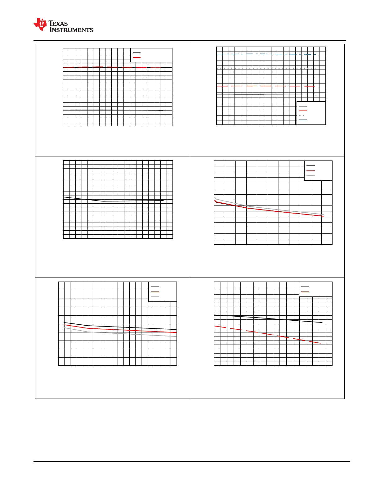
Temperature (qC)
I
VPWR
(mA)
-40 -20 0 20 40 60 80 100 120 140
6.8
7
7.2
7.4
7.6
7.8
8
8.2
8.4
8.6
8.8
9
9.2
9.4
9.6
9.8
D001
Temperature (qC)
V
VPWR
(V)
-40 -20 0 20 40 60 80 100 120 140
14
14.5
15
15.5
16
16.5
17
17.5
18
18.5
19
D002
VUVLO_Falling
VUVLO_Rising
Temperature (qC)
V
VPWR
(V)
-40 -20 0 20 40 60 80 100 120 140
24
24.6
25.2
25.8
26.4
27
27.6
28.2
28.8
29.4
30
D003
VPUV_Falling
VPUV_Rising
Temperature (qC)
I
VDD
(mA)
-40 -20 0 20 40 60 80 100 120 140
3.5
3.75
4
4.25
4.5
4.75
5
5.25
5.5
5.75
6
D004
Temperature (qC)
V
VDD
(V)
-40 -20 0 20 40 60 80 100 120 140
2
2.1
2.2
2.3
2.4
2.5
2.6
2.7
2.8
2.9
D005
VDUV_Falling
VDUV_Rising
Temperature (qC)
I
SENSE
( PA)
-40 -20 0 20 40 60 80 100 120 140
-1.2
-1.1
-1
-0.9
-0.8
-0.7
-0.6
-0.5
-0.4
-0.3
-0.2
-0.1
0
0.1
0.2
D006
Classification
Port On
Port Off
TPS23882
SLVSF21D – AUGUST 2019 – REVISED AUGUST 2020
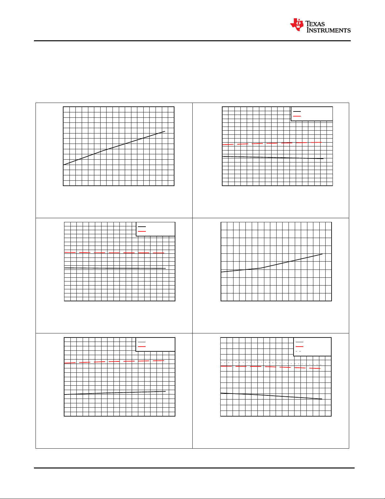
7.6 Typical Characteristics
www.ti.com
Conditions are –40 < TJ < 125 °C unless otherwise noted.V
= 3.3 V, V
VDD
VPWR
= 54 V, V
DGND
= V
AGND
, DGND,
KSENSA, KSENSB, KSENSC and KSENSD connected to AGND, and all outputs are unloaded, 2xFBn = 0.
Positive currents are into pins. RS = 0.200 Ω, to KSENSA (SEN1 or SEN2), to KSENSB (SEN3 or SEN4), to
KSENSC (SEN5 or SEN6) or to KSENSD (SEN7 or SEN8). Typical values are at 25 °C. All voltages are with
respect to AGND unless otherwise noted. Operating registers loaded with default values unless otherwise noted.
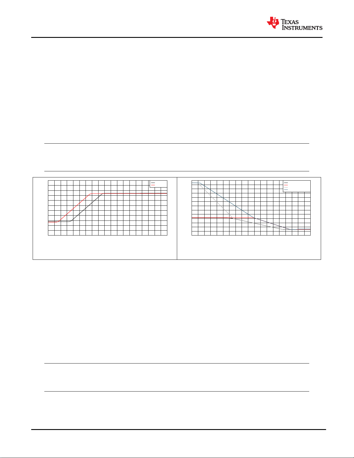
Figure 7-1. VPWR Current Consumption vs
Temperature
Figure 7-2. VPWR UVLO Thresholds vs
Temperature
Figure 7-3. VPUV Thresholds vs Temperature
Figure 7-5. VDUV Thresholds vs Temperature
14 Submit Document Feedback
Figure 7-4. VDD Current Consumption vs
Temperature
Figure 7-6. SENSE Pin Bias Current vs
Temperature
Copyright © 2020 Texas Instruments Incorporated
Product Folder Links: TPS23882
Temperature (qC)
I
DRAIN
(PA)
-40 -20 0 20 40 60 80 100 120 140
120
140
160
180
200
220
240
260
280
300
320
D007
Idiscovery_low
Idiscovery_high
Temperature (qC)
R
DET
(k:)
-40 -20 0 20 40 60 80 100 120 140
2
6
10
14
18
22
26
30
34
D008
15 k:
19 k:
26.5 k:
33 k:
Temperature (qC)
V
PORT
(V)
-40 -20 0 20 40 60 80 100 120 140
24
24.2
24.4
24.6
24.8
25
25.2
25.4
25.6
25.8
26
D009
I
CLASS
(mA)
V
CLASS
(V)
0 5 10 15 20 25 30 35 40 45 50 55
18
18.1
18.2
18.3
18.4
18.5
18.6
18.7
18.8
18.9
19
19.1
19.2
19.3
19.4
19.5
D010
-40 qC
25 qC
125 qC
I
MARK
(mA)
V
MARK
(V)
0 0.4 0.8 1.2 1.6 2 2.4 2.8 3.2 3.6 4
8.5
8.6
8.7
8.8
8.9
9
9.1
9.2
9.3
9.4
9.5
D011
-40 qC
25 qC
125 qC
Temperature (qC)
I
LIM
(mA)
-40 -20 0 20 40 60 80 100 120 140
70
70.8
71.6
72.4
73.2
74
74.8
75.6
76.4
77.2
78
D012
Class I
LIM
Mark I
LIM
www.ti.com
SLVSF21D – AUGUST 2019 – REVISED AUGUST 2020
TPS23882
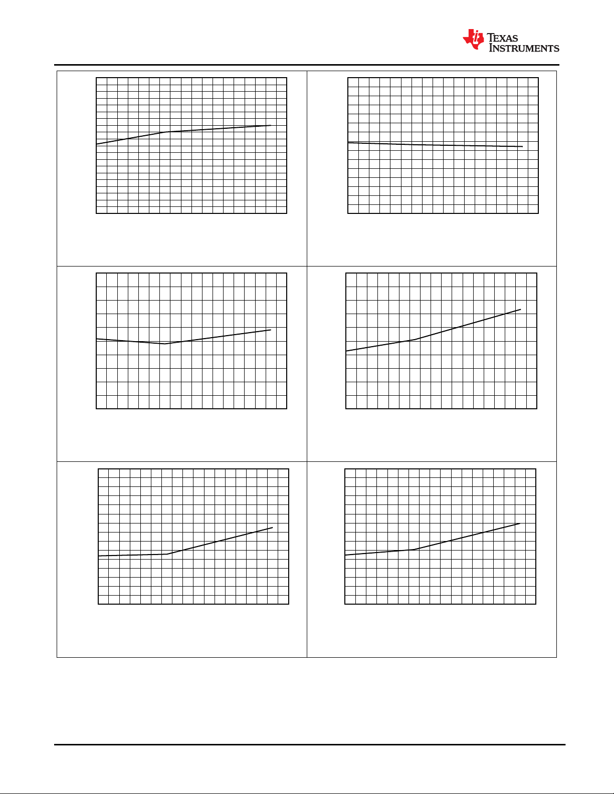
Figure 7-7. Discovery Currents vs Temperature
Figure 7-9. Discovery Open Circuit Voltage vs
Temperature
Figure 7-8. Discovery Resistance Measurement vs
Temperature
Figure 7-10. Classification Voltage vs I
CLASS
and
Temperature
Figure 7-11. Mark Voltage vs I
Copyright © 2020 Texas Instruments Incorporated
Temperature
MARK
and
Figure 7-12. Classification and Mark Current Limit
Product Folder Links: TPS23882
vs Temperature
Submit Document Feedback
15
Temperature (qC)
V
PORT
(V)
-40 -20 0 20 40 60 80 100 120 140
1.8
1.86
1.92
1.98
2.04
2.1
2.16
2.22
2.28
2.34
2.4
D013
Temperature (qC)
V
GATE
(V)
-40 -20 0 20 40 60 80 100 120 140
11.3
11.32
11.34
11.36
11.38
11.4
11.42
11.44
11.46
11.48
11.5
11.52
11.54
11.56
11.58
11.6
D014
Temperature (q C)
Port Voltage (V)
-40 -20 0 20 40 60 80 100 120 140
56.5
56.6
56.7
56.8
56.9
57
57.1
57.2
57.3
57.4
57.5
D015
Temperature (qC)
VPWR Voltage (V)
-40 -20 0 20 40 60 80 100 120 140
56.5
56.6
56.7
56.8
56.9
57
57.1
57.2
57.3
57.4
57.5
D016
Temperature (qC)
I
PORT
Measurement (mA)
-40 -20 0 20 40 60 80 100 120 140
99.5
99.6
99.7
99.8
99.9
100
100.1
100.2
100.3
100.4
100.5
100.6
100.7
100.8
100.9
101
D017
Temperature (qC)
I
PORT
Measurement (mA)
-40 -20 0 20 40 60 80 100 120 140
765
766
767
768
769
770
771
772
773
774
775
776
777
778
779
780
D018
TPS23882
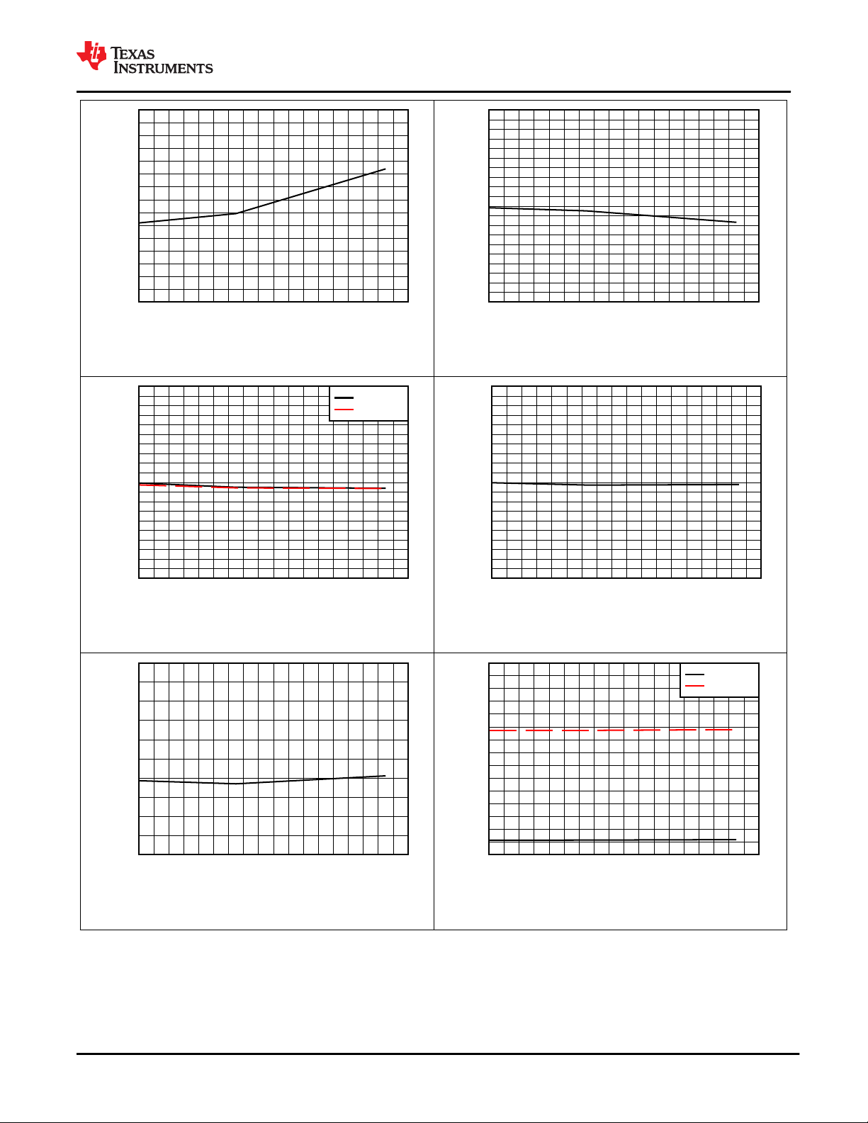
SLVSF21D – AUGUST 2019 – REVISED AUGUST 2020
www.ti.com
Figure 7-13. Power Good Threshold vs
Temperature
Figure 7-15. Port Voltage ADC Measurement vs
Temperature
Figure 7-14. Gate Voltage (Port On) vs Temperature
Figure 7-16. VPWR Voltage ADC Measurement vs
Temperature
Figure 7-17. Port Current ADC Measurement
(100mA) vs Temperature
16 Submit Document Feedback
Product Folder Links: TPS23882
Figure 7-18. Port Current ADC Measurement
(770mA) vs Temperature
Copyright © 2020 Texas Instruments Incorporated
Temperature (qC)
I
PORT
Measurement (A)
-40 -20 0 20 40 60 80 100 120 140
0.995
0.996
0.997
0.998
0.999
1
1.001
1.002
1.003
1.004
1.005
1.006
1.007
1.008
1.009
1.01
D019
Temperature (qC)
P
PCUT
(W)
-40 -20 0 20 40 60 80 100 120 140
30
30.2
30.4
30.6
30.8
31
31.2
31.4
31.6
31.8
32
D020
Temperature (qC)
I
LIM-Inrush
(mA)
-40 -20 0 20 40 60 80 100 120 140
418
418.8
419.6
420.4
421.2
422
422.8
423.6
424.4
425.2
426
D023
2xFBn = 0
2xFBn = 1
Temperature (qC)
I
LIM
(mA)
-40 -20 0 20 40 60 80 100 120 140
418
418.8
419.6
420.4
421.2
422
422.8
423.6
424.4
425.2
426
D024
Temperature (qC)
I
LIM
(A)
-40 -20 0 20 40 60 80 100 120 140
1.24
1.241
1.242
1.243
1.244
1.245
1.246
1.247
1.248
1.249
1.25
D025
Temperature (qC)
I
Port
(A)
-40 -20 0 20 40 60 80 100 120 140
1
1.05
1.1
1.15
1.2
1.25
1.3
1.35
1.4
1.45
1.5
1.55
1.6
1.65
1.7
1.75
D026
2xFBn = 0
2xFBn = 1
www.ti.com
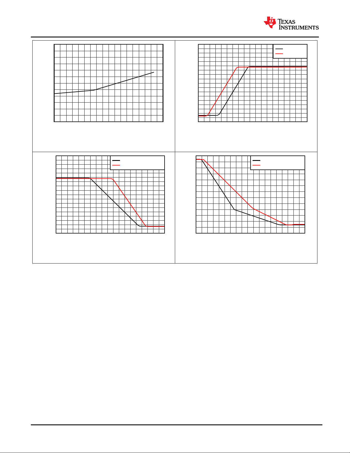
SLVSF21D – AUGUST 2019 – REVISED AUGUST 2020
TPS23882
Figure 7-19. Port Current ADC Measurement (1 A)
vs Temperature
Figure 7-21. Inrush Current Limit vs Temperature
Figure 7-20. PCut Threshold (30W) vs Temperature
Figure 7-22. 1x Mode (2xFBn = 0) Current Limit vs
Temperature
Figure 7-23. 2x Mode (2xFBn = 1) Current Limit vs
Temperature
Copyright © 2020 Texas Instruments Incorporated
Product Folder Links: TPS23882
Figure 7-24. I
Threshold vs Temperature
SHORT
Submit Document Feedback
17
Temperature (qC)
R
VPWR-DRAIN
(k:)
-40 -20 0 20 40 60 80 100 120 140
100
101
102
103
104
105
106
107
108
109
110
111
112
D027
V
PORT
(V)
I
PORT
(A)
0 6 12 18 24 30 36 42 48 54
0.1
0.15
0.2
0.25
0.3
0.35
0.4
0.45
0.5
0.55
D028
ALTIRn = 0
ALTIRn = 1
V
DRAIN
(V)
I
PORT
(A)
0 6 12 18 24 30 36 42 48 54
0.1
0.15
0.2
0.25
0.3
0.35
0.4
0.45
0.5
0.55
D029
2xFBn =0, ALTFBn = 0
2xFBn =0, ALTFBn = 1
V
DRAIN
(V)
I
PORT
(A)
0 6 12 18 24 30 36 42 48 54
0
0.1
0.2
0.3
0.4
0.5
0.6
0.7
0.8
0.9
1
1.1
1.2
1.3
D030
2xFBn =1, ALTFBn = 0
2xFBn =1, ALTFBn = 1
TPS23882
SLVSF21D – AUGUST 2019 – REVISED AUGUST 2020
www.ti.com
Figure 7-25. R
(VPWR to DRAIN) vs
OFF
Temperature
Figure 7-27. 1x Mode (2xFBn = 0) Current Foldback
vs Drain Voltage
Figure 7-26. Inrush Current Foldback vs Port
Voltage
Figure 7-28. 2x Mode (2xFBn = 1) Current Foldback
vs Drain Voltage
18 Submit Document Feedback
Product Folder Links: TPS23882
Copyright © 2020 Texas Instruments Incorporated
t
fSDA
t
fo
Repeated
Start Condition
t
LOW
t
SU,DAT
t
HD,DAT
SCL
SDAI/
SDAO
t
r
t
f
t
rSDA
t
HIGH
Start Condition
Stop Condition
Start Condition
t
SU,STO
t
HD,STA
t
SU,STA
t
BUF
SEN
GATE
0 V
0 V
V
LIM
V
CUT
t
OVLD
www.ti.com
8 Parameter Measurement Information
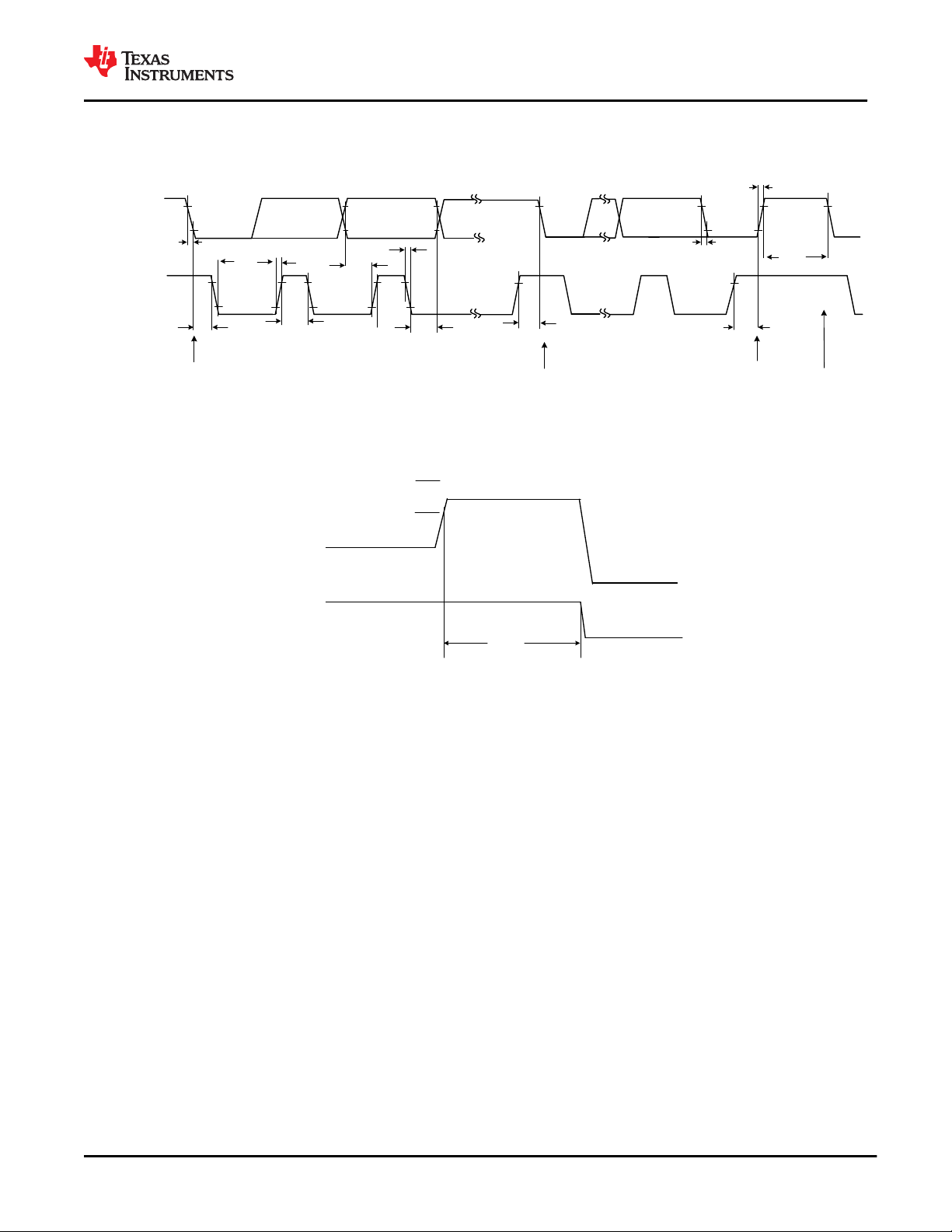
8.1 Timing Diagrams
Figure 8-1. I2C Timings
SPACE
SLVSF21D – AUGUST 2019 – REVISED AUGUST 2020
TPS23882
Figure 8-2. Overcurrent Fault Timing
Copyright © 2020 Texas Instruments Incorporated
Product Folder Links: TPS23882
Submit Document Feedback
19
t
pon
V
PORT
0 V
Four-point
detection
t
DET
t
CLE-1
Class
V
CLASS
V
MARK
Mark
Port turn-on
t
pon
V
PORT
0 V
Four-point
detection
t
DET
t
CLE-1
t
ME
Class
V
CLASS
V
MARK
Mark
Port turn-on
t
CLE
TPS23882
SLVSF21D – AUGUST 2019 – REVISED AUGUST 2020
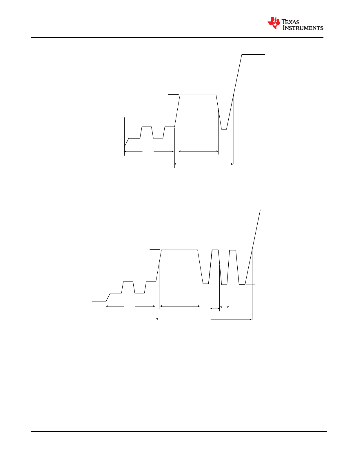
Figure 8-3. 2-Pair Detection, 1-Event Classification and Turn On
SPACE
www.ti.com
Figure 8-4. 2-Pair Detection, 3-Event Classification and Turn On
SPACE
20 Submit Document Feedback
Product Folder Links: TPS23882
Copyright © 2020 Texas Instruments Incorporated

www.ti.com
SLVSF21D – AUGUST 2019 – REVISED AUGUST 2020
TPS23882
9 Detailed Description
9.1 Overview
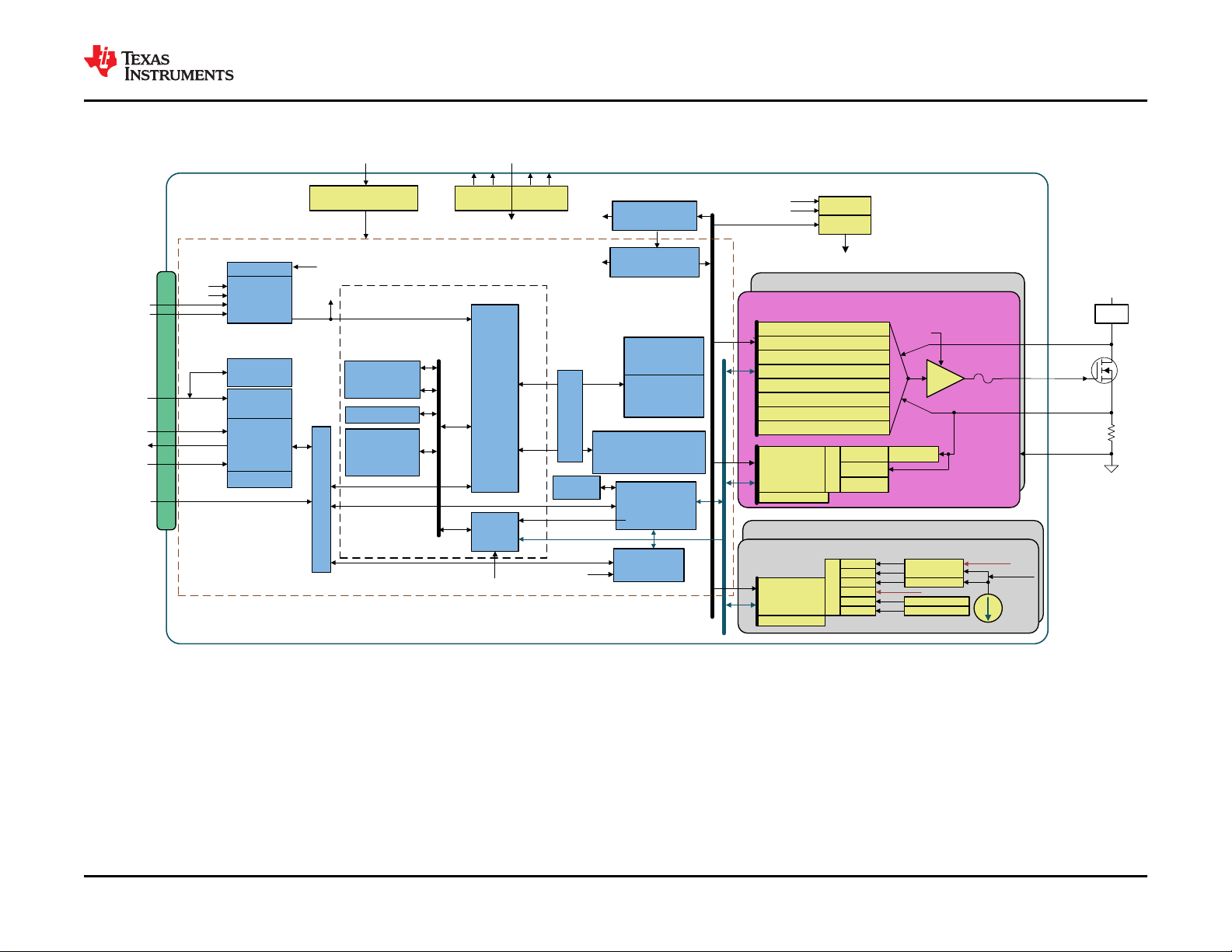
The TPS23882 is an eight-channel PSE for Power over Ethernet applications. Each of the eight channels
provides detection, classification, protection, and shutdown in compliance with the IEEE 802.3bt standard.
Basic PoE features include the following:
• Performs high-reliability 4-point load detection
• Performs multi-finger classification including the 100-ms long first class finger for Autoclass discovery and to
identify as a 802.3bt complainant PSE
• Enables power with protective fold-back current limiting, and an adjustable P
• Shuts down during faults such as overcurrent or outputs shorts
• Performs a maintain power signature function to ensure power is removed if the load is disconnected
• Undervoltage lockout occurs if VPWR falls below V
(typical 26.5 V).
PUV_F
Enhanced features include the following:
• Programable SRAM memory
• Dedicated 14-bit integrating current ADCs per port
• Port re-mapping capability
• 8- and 16-bit access mode selectable
• 1- and 3-bit port shutdown priority
threshold
CUT
9.1.1 Operating Modes
9.1.1.1 Auto
The port performs detection and classification (if valid detection occurs) continuously. Registers are updated
each time a detection or classification occurs. The port power is automatically turned on based on the Power
Allocation settings in register 0x29 if a valid classification is measured.
9.1.1.2 Semiauto
The port performs detection and classification (if valid detection occurs) continuously. Registers are updated
each time a detection or classification occurs. The port power is not automatically turned on. A Power Enable
command is required to turn on the port.
9.1.1.3 Manual/Diagnostic
The use of this mode is intended for system diagnostic purposes only in the event that ports cannot be
powered in accordance with the IEEE 802.3bt standard from Semiauto or Auto modes.
The port performs the functions as configured in the registers. There is no automatic state change. Singular
detection and classification measurements will be performed when commanded. Ports will be turned on
immediately after a Power Enable command without any detection or classification measurements. Even though
multiple classification events may be provided, the port voltage will reset immediately after the last finger,
resetting the PD.
9.1.1.4 Power Off
The port is powered off and does not perform a detection, classification, or power-on. In this mode, Status and
Enable bits for the associated port are reset.
Copyright © 2020 Texas Instruments Incorporated
Product Folder Links: TPS23882
Submit Document Feedback
21

TPS23882
SLVSF21D – AUGUST 2019 – REVISED AUGUST 2020
www.ti.com
9.1.2 PoE Compliance Terminology
With the release of the IEEE 802.3bt standard, compliant PoE equipment has expanded to include four different
"Types" of devices that support power over 2-Pair or 4-Pair, in either Single or Dual signature configurations, with
classifications ranging from 0 to 8. Different manufactures have used varying terminology over time to describe
their equipment capabilities, and it can become difficult to identify how to correctly categorize and brand a
particular piece of equipment. For this reason and in conjunction with the Ethernet Alliance (EA), the industry
leading providers of PoE equipment and devices have agreed to transition to using the "PoE 1" and "PoE 2"
banding per the table below Table 9-1.
SPACE
Table 9-1. Summary Table of PoE Compliance Terminology
Brand /
Acronym
PoE 1
PoE 2 802.3bt 145 Power over Ethernet
(1) "DS" is used to designate "Dual Signature" PDs
IEEE
Standard
802.3af
802.3at 2 0 - 4
Clause Clause Title Types Classes EA Certified Logo
33
Power over Ethernet over 2-
Pairs
1 0 - 3
3
4
1 - 6, or 1-4
7 - 8, or 5
DS
DS
Gen 1 Class 1-4
(1)
Gen 2 Class 1-8
(1)
Note
By design PoE 2 PSEs are fully interoperable with any existing PoE 1 equipment, and although not all
functionality may be enabled, PoE 2 PDs connected to PoE 1 PSEs are required to limit their power
consumption to the PSE presented power capabilities see Power Allocation and Power Demotion.
9.1.3 PoE 2 Type-3 2-Pair PoE
Upon release of the new IEEE 802.3bt standard, the IEEE introduced two new "Types" of PoE equipment. The
addition of Type-3 and Type-4 equipment are most commonly associated with the addition of 4-Pair PoE and
their available power increases of to up to 90 W sourced from a PSE port. However, the new PoE 2 Type-3
designation also applies to new 2-Pair PoE equipment as well. Most notably, the new 802.3bt standard supports
a reduced T
time (6 ms vs. 60 ms) and a new feature called Autoclass, and by definition any device that
MPS
supports these new features is designated as Type-3 equipment even if power is only provided over 2-pairs (one
alternative pairset) in an ethernet cable. Since the TPS23882 supports these new features including its use of
the 100ms long first class finger to identify itself as an IEEE 802.3bt PSE, it is officially classified as a Type-3
PSE even through power delivery is limited to 2-pair.
Please note that as the 802.3at standard created "type-2" equipment that was fully interoperable with the
previous PoE 1 Type-1 (802.3af) equipment, any new 802.3bt Type-3 equipment including the TPS23882 is fully
operable with any existing PoE 1 Type-1 (.af) and Type-2 (.at) equipment.
SPACE
22 Submit Document Feedback
Copyright © 2020 Texas Instruments Incorporated
Product Folder Links: TPS23882

www.ti.com
SLVSF21D – AUGUST 2019 – REVISED AUGUST 2020
TPS23882
9.1.4 Requested Class versus Assigned Class
The requested class is the classification the PSE measures during mutual identification prior to turnon, whereas
the assigned class is the classification level the channel was powered on with based on the power allocation
setting in register 0x29h. In most cases where the power allocation equals or exceeds the requested class, the
requested and assigned classes will be the same. However, in the case of power demotion, these values will
differ.
For example: If a 4-pair Class 8 PD is connected to a 30 W (Class 4) configured PSE port, the requested class
reports "Class 8", while the assigned class reports "Class 4".
The requested classification results are available in registers 0x0C-0F
The assigned classification results are available in registers 0x4C-4F
Note
There is no Assigned Class assigned for ports/channels powered out of Manual/Diagnostic mode.
9.1.5 Power Allocation and Power Demotion
The Power Allocation settings in register 0x29 sets the maximum power level a port will power on. Settings for
each Class level from 2-pair 4 W (Class 1) up to 2-pair 30 W (Class 4) have been provided to maximize system
design flexibility.
Note
The Power Allocation settings in register 0x29 do not set the power limit for a given port. The port and
channel power limiting is configured with the 2P (registers 0x1E- x 21) policing registers
During a turn on attempt, if a PD presents a classification level greater than the power allocation setting for a
port, the TPS23882 limits the number of classification fingers presented to the PD prior to turn on based on the
power allocation settings in register 0x29. This behavior is called Power Demotion as it is the number of fingers
presented to the PD that sets the maximum level of power the PD is allowed to draw before the PSE is allowed
to disable it.
Note
The IEEE 802.3 standard requires PDs that are power demoted by a PSE to limit their total power
draw below the Type/class level set by the number of fingers presented by the PSE during mutual
identification.
In a 2-pair system, Power demotion is limited to either 30 W (3-fingers) or 15.4 W (1-finger) as there is
no other physical means of indicating to a PD over the physical layer that less than 15.4 W is
available.
If register 0x29 is configured for either 4 W (class 1) or 7 W (Class 2), and a Class 3 or higher device
is connected, the port will not be powered and a Start Fault will be reported along with an "Insufficient
Power" indication provided in register 0x24.
Table 9-2. 2-Pair Power Demotion Table
Power Allocation
Register 0x29
2-Pair 4 W Class 1
2-Pair 7 W Class 1 Class 2
2-Pair 15.5 W Class 1 Class 2 Class 3 Class 3 Class 3
2-Pair 30 W Class 1 Class 2 Class 3 Class 4 Class 4
Class 1 PD Class 2 PD Class 3 PD Class 4 PD Class 5+ PDs
Assigned Class Value (based on the PD connected at the port)
Start Fault
Insufficient Power
Start Fault
Insufficient Power
Start Fault
Insufficient Power
Start Fault
Insufficient Power
Start Fault
Insufficient Power
Start Fault
Insufficient Power
Start Fault
Insufficient Power
Copyright © 2020 Texas Instruments Incorporated
Product Folder Links: TPS23882
Submit Document Feedback
23

TPS23882
SLVSF21D – AUGUST 2019 – REVISED AUGUST 2020
www.ti.com
9.1.6 Programmable SRAM
The TPS23882 device has been designed to include programmable SRAM that accommodates future firmware
updates to support interoperability and/or compliance issues that may arise as new equipment is introduced in
conjunction with the release of the IEEE 802.3bt standard.
Note
The latest version of firmware and SRAM release notes may be accessed from the TI mySecure
Software webpage.
The SRAM Release Notes and ROM Advisory document includes more detailed information regarding
any know issues and changes that were associated with each firmware release.
Upon power up, it is recommended that the TPS23882 device's SRAM be programmed with the latest version of
SRAM code via the I2C to ensure proper operation and IEEE complaint performance. All I2C traffic other than
those commands required to program the SRAM should be deferred until after the SRAM programming
sequences are completed.
For systems that include multiple TPS23882 devices, the 0x7F "global" broadcast I2C address may be used to
programmed all of the devices at the same time.
For more detailed instructions on the SRAM programing procedures please refer to Section 9.6.2.67 and the
How to Load TPS2388x SRAM Code document on TI.com.
24 Submit Document Feedback
Copyright © 2020 Texas Instruments Incorporated
Product Folder Links: TPS23882
Common Functions for Ports 5-8
Common Functions for Ports1-4
Port 2-8 Analog Control Functions
Port 1 Analog Control Functions
RANGE
SELECT
14 Bit ADC
(Current)
2X Power
ICLASS
Internal Rails
Good
Temp
VEE
Vds
BIT
4:1 MUX
PTAT DIODES
Analog BIT MUX
RANGE SELECT
14 Bit ADC
(Voltage)
Variable Averager
Vdisco
PORT DIFF
AMP
Vport
Foldback Schedulers
Fast Ishort Protection
dv/dt ramping control
Rapid Overload recovery
GATEx
Enable
SENx
Ilim
320Hz LPFIPORT
BIT
DISCRETE IO CONDITIONERS
RST
to blks
CPU Watchdog
Register File
I2C Interface
External Data
Memory Bus
CPU
Interrupt
Controller
7 bit address
Select
Timers
SFR
BUS
MCU
Scan + Digital
Test
SCL Watchdog
CPU SRAM
ROM
IRAM
Bus
Prog
Mem
Bus
Memory BIST
Bus IF
Analog TRIM
Class Current Limit
Class Port Voltage Control
Variable Averager
SDAI
SDAO
SCL
Firmware Controlled
Update from register File
LDO
UVLO
VDD
Internal Oscillator
RESETB
OSS
RST Block
PG
CLK OK
Clock Distribution
DRAINx
KSENSEx
CLK
to blks
CLK OK
PG
OSS
INT
A1-A4
OSS/
POR
VPWR
IDET
FW Registers
SFR
With BIST
REMAP
Fuse-able
Disconnect
VPWR
VPWR Divider
VPWR
NC
VPWR
1/3
1/3 2/3
2/3
NC NCNC
SRAM
Load at Power
up into holding
latches
VDD
Program Memory
Gm
DRIVER
R
SENSE
GND
PD
LOAD
V48
V48
DRAIN1-4
www.ti.com
9.2 Functional Block Diagram
SLVSF21D – AUGUST 2019 – REVISED AUGUST 2020
TPS23882
Copyright © 2020 Texas Instruments Incorporated
Product Folder Links: TPS23882
Submit Document Feedback
25
IDLE
START bits
SC 2
one-bit
duration
t
bit_OSS
t
OSS_IDL
3.3 V
0 V
SC 1
OSS
SC 0
Shutdown Code
GATE
t
OSS_OFF
IDLE
t
r_OSS
t
f_OSS
TPS23882
SLVSF21D – AUGUST 2019 – REVISED AUGUST 2020
www.ti.com
9.3 Feature Description
9.3.1 Port Remapping
The TPS23882 provides port remapping capability, from the logical ports to the physical channels and pins.
The remapping is between any channel of a 4-port group (1 to 4, 5 to 8).
The following example is applicable to 0x26 register = 00111001, 00111001b.
• Logical port 1 (5) ↔ Physical channel 2 (6)
• Logical port 2 (6) ↔ Physical channel 3 (7)
• Logical port 3 (7) ↔ Physical channel 4 (8)
• Logical port 4 (8) ↔ Physical channel 1 (5)
Note
The device ignores any remapping command unless all four ports are in off mode.
If the TPS23882 receives an incorrect configuration, it ignores the incorrect configuration and retains the
previous configuration. The ACK is sent as usual at the end of communication. For example, if the same
remapping code is received for more than one port, then a read back of the Re-Mapping register (0x26) would
be the last valid configuration.
Note that if an IC reset command (1Ah register) is received, the port remapping configuration is kept unchanged.
However, if there is a Power-on Reset or if the
a default value.
RESET pin is activated, the Re-Mapping register is reinitialized to
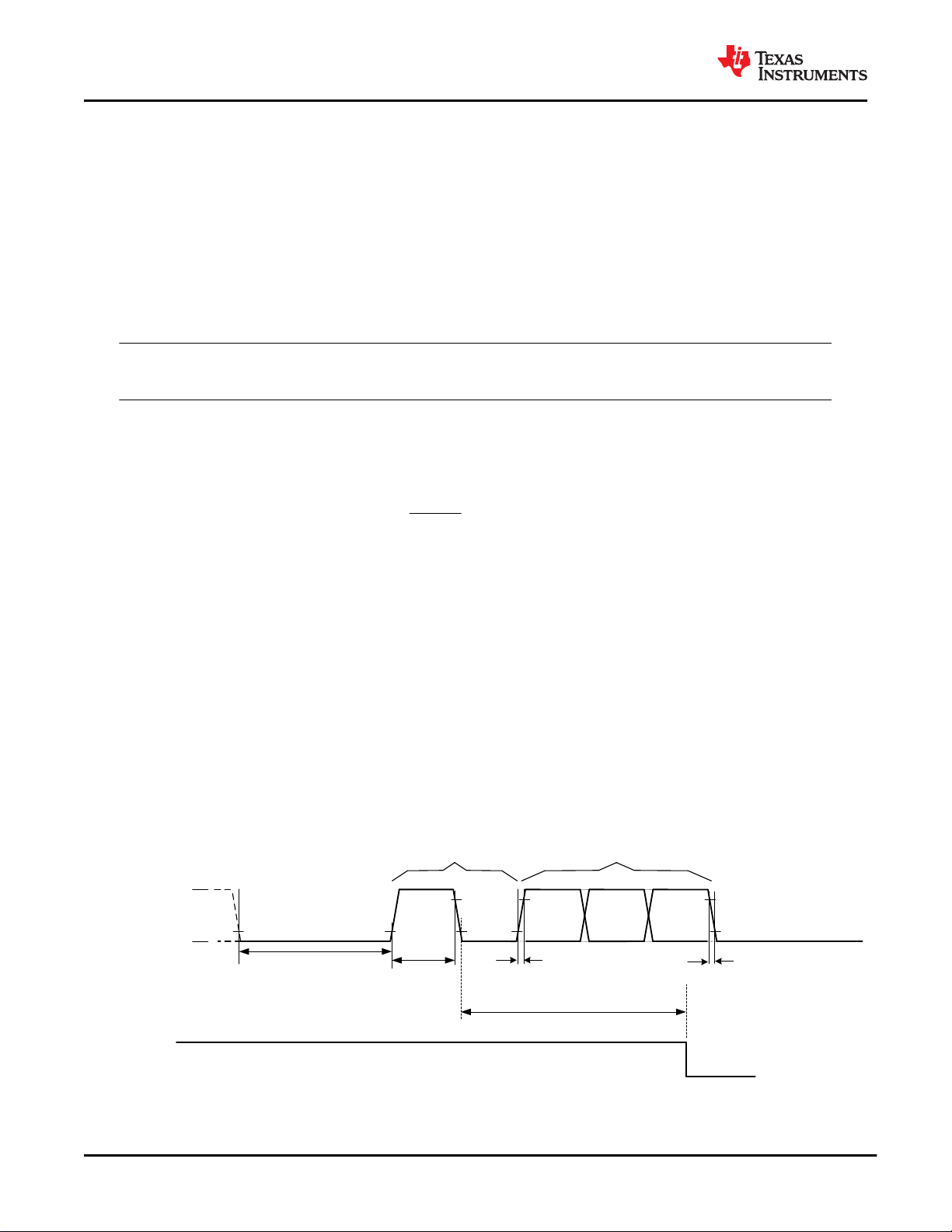
9.3.2 Port Power Priority
The TPS23882 supports 1- and 3-bit shutdown priority, which are selected with the MbitPrty bit of General Mask
register (0x17).
The 1-bit shutdown priority works with the Port Power Priority (0x15) register. An OSSn bit with a value of 1
indicates that the corresponding port is treated as low priority, while a value of 0 corresponds to a high priority.
As soon as the OSS input goes high, the low-priority ports are turned off.
The 3-bit shutdown priority works with the Multi Bit Power Priority (0x27/28) register, which holds the priority
settings. A port with “000” code in this register has highest priority. Port priority reduces as the 3-bit value
increases, with up to 8 priority levels. See Figure 9-1.
The multi bit port priority implementation is defined as the following:
• OSS code ≤ Priority setting (0x27/28 register): Port is disabled
• OSS code > Priority setting (0x27/28 register): Port remains active
26 Submit Document Feedback
Figure 9-1. Multi Bit Priority Port Shutdown if Lower-Priority Port
Product Folder Links: TPS23882
Copyright © 2020 Texas Instruments Incorporated

www.ti.com
SLVSF21D – AUGUST 2019 – REVISED AUGUST 2020
TPS23882
Note
Prior to setting the MbitPrty bit from 0 to 1, make sure the OSS input is in the idle (low) state for a
minimum of 200 µs, to avoid any port misbehavior related to loss of synchronization with the OSS bit
stream.
Note
The OSS input has an internal 1-µs to 5-µs deglitch filter. From the idle state, a pulse with a longer
duration is interpreted as a valid start bit. Ensure that the OSS signal is noise free.
9.3.3 Analog-to-Digital Converters (ADC)
The TPS23882 features 10 multi-slope integrating converters. Each of the first eight converters is dedicated to
current measurement for one channel and operate independently to perform measurements during classification
and when the channel is powered on. When the channel is powered, the converter is used for current (100-ms
averaged) monitoring, power policing, and DC disconnect. Each of the last two converters are shared within a
group of four channels for discovery (16.6-ms averaged), port powered voltage monitoring, power-good status,
and FET short detection. These converters are also used for general-purpose measurements including input
voltage (1 ms) and die temperature.
The ADC type used in the TPS23882 differs from other similar types of converters in that the ADCs continuously
convert while the input signal is sampled by the integrator, providing inherent filtering over the conversion period.
The typical conversion time of the current converters is 800 µs, while the conversion time is 1 ms for the other
converters. Powered-device detection is performed by averaging 16 consecutive samples which provides
significant rejection of noise at 50-Hz or 60-Hz line frequency. While a port is powered, digital averaging provides
a channel current measurement integrated over a 100-ms time period. Note that an anti-aliasing filter is present
for powered current monitoring.
Note
During powered mode, current conversions are performed continuously. Also, in powered mode, the
t
timer must expire before any current or voltage ADC conversion can begin.
START
9.3.4 I2C Watchdog
An I2C Watchdog timer is available on the TPS23882 device. The timer monitors the I2C, SCL line for clock
edges. When enabled, a timeout of the watchdog resets the I2C interface along with any active ports. This
feature provides protection in the event of a hung software situation or I2C bus hang-up by slave devices. In the
latter case, if a slave is attempting to send a data bit of 0 when the master stops sending clocks, then the slave
my drive the data line low indefinitely. Because the data line is driven low, the master cannot send a STOP to
clean up the bus. Activating the I2C watchdog feature of the TPS23882 clears this deadlocked condition. If the
timer of two seconds expires, the ports latch off and the WD status bit is set. Note that WD Status will be set
even if the watchdog is not enabled. The WD status bit may only be cleared by a device reset or writing a 0 to
the WDS status bit location. The 4-bit watchdog disable field shuts down this feature when a code of 1011b is
loaded. This field is preset to 1011b whenever the TPS23882 is initially powered. See I2C WATCHDOG Register
for more details.
Copyright © 2020 Texas Instruments Incorporated
Product Folder Links: TPS23882
Submit Document Feedback
27
V
PORT
(V)
I
PORT
(A)
0 3 6 9 12 15 18 21 24 27 30 33 36 39 42 45 48 51 54 57
0
0.05
0.1
0.15
0.2
0.25
0.3
0.35
0.4
0.45
0.5
0.55
D100
ALTIRn = 0
ALTIRn = 1
V
DRAIN
(V)
I
PORT
(A)
0 3 6 9 12 15 18 21 24 27 30 33 36 39 42 45 48 51 54 57
0
0.1
0.2
0.3
0.4
0.5
0.6
0.7
0.8
0.9
1
1.1
1.2
1.3
D200
2xFBn =0, ALTFBn = 0
2xFBn =0, ALTFBn = 1
2xFBn =1, ALTFBn = 0
2xFBn =1, ALTFBn = 1
TPS23882
SLVSF21D – AUGUST 2019 – REVISED AUGUST 2020
www.ti.com
9.3.5 Current Foldback Protection
The TPS23882 features two types of foldback mechanisms for complete MOSFET protection.
During inrush, at channel turn on, the foldback is based on the channel voltage as shown in Figure 9-2. Note that
the inrush current profile remains the same, regardless of the state of the 2xFBn bits in register 0x40.
After the channel is powered and the Power Good is valid, a dual-slope operational foldback is used, providing
protection against partial and total short-circuit at port output, while still being able to maintain the PD powered
during normal transients at the PSE input voltage. Note that setting the 2xFBn bit selects the 2× curve and
clearing it selects the 1× curve. See Figure 9-3.
In addition to the default foldback curves, the TPS23882 has individually enabled alternative foldback curves for
both inrush and powered operation. These curves have been designed to accommodate certain loads that do
not fully comply with the IEEE standard and requires additional power to be turned on or remain powered. See
Figure 9-2 and Figure 9-3.
Note
If using the Alternative Foldback curves (ALTIRn or ALTFBn = 1), designers need to account for the
additional power dissipation that can occur in the FETs under these conditions.
Figure 9-2. Foldback During Inrush (at Port Turn
On): I
LIM
vs V
9.4 Device Functional Modes
9.4.1 Detection
To eliminate the possibility of false detection, the TPS23882 uses a TI proprietary 4-point detection method to
determine the signature resistance of the PD device. A false detection of a valid 25-kΩ signature can occur with
2-point detection type PSEs in noisy environments or if the load is highly capacitive.
Detection 1 and Detection 2 are merged into a single detection function which is repeated. Detection 1 applies I1
(160 μA) to a channel, waits approximately 60 ms, then measures the channel voltage (V1) with the integrating
ADC. Detection 2 then applies I2 (270 μA) to the channel, waits another approximately 60 ms, then measures
the channel voltage again (V2). The process is then repeated a second time to capture a third (V3) and fourth
(V4) channel voltage measurements. Multiple comparisons and calculations are performed on all four
measurement point combinations to eliminate the effects of a nonlinear or hysteretic PD signature. The resulting
channel signature is then sorted into the appropriate category.
The detection resistance measurement result is also available in the Channel Detect Resistance
registers (0x44 - 0x47).
9.4.2 Classification
Hardware classification (class) is performed by supplying a voltage and sampling the resulting current. To
eliminate the high power of a classification event from occurring in the power controller chip, the TPS23882 uses
the external power FET for classification.
28 Submit Document Feedback
port
Figure 9-3. Foldback When the Port is Already ON:
I
vs V
LIM
drain
Note
Copyright © 2020 Texas Instruments Incorporated
Product Folder Links: TPS23882

www.ti.com
SLVSF21D – AUGUST 2019 – REVISED AUGUST 2020
TPS23882
During classification, the voltage on the gate node of the external MOSFET is part of a linear control loop. The
control loop applies the appropriate MOSFET drive to maintain a differential voltage between VPWR and DRAIN
of 18.5 V. During classification the voltage across the sense resistor in the source of the MOSFET is measured
and converted to a class level within the TPS23882. If a load short occurs during classification, the MOSFET
gate voltage reduces to a linearly controlled, short-circuit value for the duration of the class event.
Classification results are read through the I2C Detection Event and Channel-n Discovery Registers. The
TPS23882 also supports 1, and 3 finger classification for PDs ranging from Class 0 through Class 4, using the
Power Enable and Port Power Allocation registers. Additionally, by providing a 3rdclass finger during discovery in
Semi Auto mode, the TPS23882 is capable of identifying if a 4-pair Class 5-8 PD is connected to the port.
9.4.3 DC Disconnect
Disconnect is the automated process of turning off power to the port. When the port is unloaded or at least falls
below minimum load, it is required to turn off power to the port and restart detection. In DC disconnect, the
voltage across the sense resistors is measured. When enabled, the DC disconnect function monitors the sense
resistor voltage of a powered port to verify the port is drawing at least the minimum current to remain active. The
T
timer counts up whenever the port current is below the disconnect threshold (6.5 mA typical). If a timeout
DIS
occurs, the port is shut down and the corresponding disconnect bit in the Fault Event Register is set. In the case
of a PD implementing MPS (maintain Power Signature) current pulsing, the T
counter is reset each time the
DIS
current goes continuously higher than the disconnect threshold for at least 3 ms.
The T
duration is set by the T
DIS
Bits of the Timing Configuration register (0x16).
MPDO
9.5 I2C Programming
9.5.1 I2C Serial Interface
The TPS23882 features a 3-wire I2C interface, using SDAI, SDAO, and SCL. Each transmission includes a
START condition sent by the master, followed by the device address (7-bit) with R/W bit, a register address byte,
then one or two data bytes and a STOP condition. The recipient sends an acknowledge bit following each byte
transmitted. SDAI/SDAO is stable while SCL is high except during a START or STOP condition.
Figure 9-4 and Figure 9-5 show read and write operations through I2C interface, using configuration A or B (see
Table 9-23 for more details). The parametric read operation is applicable to ADC conversion results. The
TPS23882 features quick access to the latest addressed register through I2C bus. When a STOP bit is received,
the register pointer is not automatically reset.
It is also possible to perform a write operation to many TPS23882 devices at the same time. The slave address
during this broadcast access is 0x7F, as shown in Section 9.6.2.13. Depending on which configuration (A or B) is
selected, a global write proceeds as following:
• Config A: Both 4-port devices (1 to 4 and 5 to 8) are addressed at same time.
• Config B: The whole device is addressed.
Copyright © 2020 Texas Instruments Incorporated
Product Folder Links: TPS23882
Submit Document Feedback
29
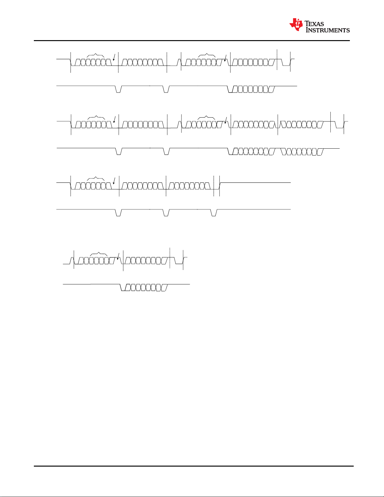
Write Cycle
0 1 A4 A3 A2 A1 A0 R/W D7 D6 D5 D4 D3 D2 D1 D0
Start Bit
Slave Address
R/W=0
R/W
Bit
Data from
Host to Slave
Stop Bit
Ack Bit
Ack Bit
Ack Bit
C7
C6
C5
C4
C3
C2
C1
C0
Command Code
0 1 A4 A3 A2 A1 A0 R/W 0 1 A4 A3 A2 A1 A0
R/W
D7 D6 D5 D4 D3 D2 D1 D0
R/W
Bit
Start Bit
Slave Address
R/W=0
Command Code
Slave Address
R/W=1
R/W
Bit
Data from
Slave to Host
Ack Bit
Ack Bit
Ack Bit
NAck Bit
Stop Bit
C7
C6
C5
C4
C3
C2
C1
C0
D7 D6 D5 D4 D3 D2 D1 D0
Non-Parametric
Read Cycle
Parametric
Read Cycle
SDAO
0 1 A4 A3 A2 A1 A0 R/W 0 1 A4 A3 A2 A1 A0
R/W
D7 D6 D5 D4 D3 D2 D1 D0
R/W
Bit
Start Bit
Slave Address
R/W=0
Command Code
Slave Address
R/W=1
R/W
Bit
LSByte Data from
Slave to Host
Ack Bit
Ack Bit
Bit
SDAI
NAck Bit
Stop Bit
C7
C6
C5
C4
C3
C2
C1
C0
Ack
Bit
Ack
D7 D6 D5 D4 D3 D2 D1 D0
D7 D6 D5 D4 D3 D2 D1 D0
D7 D6 D5 D4 D3 D2 D1 D0
SDAO
SDAI
SDAO
SDAI
Repeated
Start Bit
Repeated
Start Bit
MSByte Data from
Slave to Host
0 1 A4 A3 A2 A1 A0 R/W
D7 D6 D5 D4 D3 D2 D1 D0
Slave Address
R/W=1
R/W
Bit
Data from
Slave to Host
Start Bit
Ack Bit
NAck Bit
Stop Bit
D7 D6 D5 D4 D3 D2 D1 D0
Quick Read Cycle
(latest addressed register)
SDAO
SDAI
Address
Pins
Address
Pins
Address
Pins
Address
Pins
Address
Pins
Address
Pins
TPS23882
SLVSF21D – AUGUST 2019 – REVISED AUGUST 2020
www.ti.com
Figure 9-4. I2C interface Read and Write Protocol – Configuration A
30 Submit Document Feedback
Copyright © 2020 Texas Instruments Incorporated
Product Folder Links: TPS23882

Write Cycle
0 1 A4 A3 A2 A1 0 R/W D7 D6 D5 D4 D3 D2 D1 D0
Start Bit
Slave Address
R/W=0
R/W
Bit
Port 4-1 Data from
Host to Slave
Stop Bit
Ack Bit
Ack Bit
Ack Bit
C7
C6
C5
C4
C3
C2
C1
C0
Command Code
0 1 A4 A3 A2 A1 0 R/W 0 1 A4 A3 A2 A1 0
R/W
D7 D6 D5 D4 D3 D2 D1 D0
R/W
Bit
Start Bit
Slave Address
R/W=0
Command Code
Slave Address
R/W=1
R/W
Bit
Port 4-1 Data from
Slave to Host
Ack Bit
Ack Bit
Ack Bit
C7
C6
C5
C4
C3
C2
C1
C0
D7 D6 D5 D4 D3 D2 D1 D0
Non-Parametric
Read Cycle
Parametric
Read Cycle
SDAO
0 1 A4 A3 A2 A1 0 R/W 0 1 A4 A3 A2 A1 0
R/W
D7 D6 D5 D4 D3 D2 D1 D0
R/W
Bit
Start Bit
Slave Address
R/W=0
Command Code
Slave Address
R/W=1
R/W
Bit
Port 4-1
LSByte Data from
Slave to Host
Ack Bit
Ack Bit
Bit
SDAI
C7
C6
C5
C4
C3
C2
C1
C0
Ack
Bit
Ack
D7 D6 D5 D4 D3 D2 D1 D0
D7 D6 D5 D4 D3 D2 D1 D0
D7 D6 D5 D4 D3 D2 D1 D0
SDAO
SDAI
SDAO
SDAI
Repeated
Start Bit
Repeated
Start Bit
Port 4-1
MSByte Data from
Slave to Host
Address
Pins
Address
Pins
NAck Bit
Stop Bit
Bit
Ack
D7 D6 D5 D4 D3 D2 D1 D0
D7 D6 D5 D4 D3 D2 D1 D0
Port 8-5 Data from
Slave to Host
Address
Pins
Address
Pins
D7 D6 D5 D4 D3 D2 D1 D0
Port 8-5
LSByte Data from
Slave to Host
NAck Bit
Stop Bit
Bit
Ack
D7 D6 D5 D4 D3 D2 D1 D0
D7 D6 D5 D4 D3 D2 D1 D0
D7 D6 D5 D4 D3 D2 D1 D0
Port 8-5
MSByte Data from
Slave to Host
SDAO
SDAI
Ack Bit
...
...
Address
Pins
D7 D6 D5 D4 D3 D2 D1 D0
Ack Bit
Port 8-5 Data from
Host to Slave
www.ti.com
SLVSF21D – AUGUST 2019 – REVISED AUGUST 2020
TPS23882
Figure 9-5. I2C interface Read and Write Protocol – Configuration B
Copyright © 2020 Texas Instruments Incorporated
Product Folder Links: TPS23882
Submit Document Feedback
31

TPS23882
SLVSF21D – AUGUST 2019 – REVISED AUGUST 2020
www.ti.com
9.6 Register Maps
9.6.1 Complete Register Set
Table 9-3. Main Registers
Cmd
Code
00h INTERRUPT RO 1 1000,0000b
01h INTERRUPT MASK R/W 1 1000,0000b SUMSK STMSK IFMSK CLMSK DEMSK DIMSK PGMSK PEMSK
02h
03h CoR 1 PGC4 PGC3 PGC2 PGC1 PEC4 PEC3 PEC2 PEC1
04h
05h CoR 1 CLSC4 CLSC3 CLSC2 CLSC1 DETC4 DETC3 DETC2 DETC1
06h
07h CoR 1 DISF4 DISF3 DISF2 DISF1 PCUT4 PCUT3 PCUT2 PCUT1
08h
09h CoR 1 ILIM4 ILIM3 ILIM2 ILIM1 STRT4 STRT3 STRT2 STRT1
0Ah
0Bh CoR 1
0Ch
0Dh
0Eh
0Fh
10h POWER STATUS RO 1 0000,0000b PG4 PG3 PG2 PG1 PE4 PE3 PE2 PE1
11h PIN STATUS RO 1 0,A[4:0],0,0 Rsvd SLA4 SLA3 SLA2 SLA1 SLA0 Rsvd Rsvd
12h OPERATING MODE R/W 1 0000,0000b Channel 4 Mode Channel 3 Mode Channel 2 Mode Channel 1 Mode
13h
14h
15h
16h TIMING CONFIG R/W 1 0000,0000b TLIM TSTART TOVLD TMPDO
17h GENERAL MASK R/W 1 1000,0000b INTEN Rsvd nbitACC MbitPrty CLCHE DECHE Rsvd
Register or
Command Name
POWER EVENT
DETECTION
EVENT
FAULT EVENT
START/ILIM EVENT
SUPPLY/FAULT
EVENT
CHANNEL 1
DISCOVERY
CHANNEL 2
DISCOVERY
CHANNEL 3
DISCOVERY
CHANNEL 4
DISCOVERY
DISCONNECT
ENABLE
DETECT/CLASS
ENABLE
PWRPR/PCUT
DISABLE
I2C
Data
R/W
RO 1
RO 1
RO 1
RO 1
RO 1
RO 1 0000,0000b Requested CLASS Channel 1 DETECT Channel 1
RO 1 0000,0000b Requested CLASS Channel 2 DETECT Channel 2
RO 1 0000,0000b Requested CLASS Channel 3 DETECT Channel 3
RO 1 0000,0000b Requested CLASS Channel 4 DETECT Channel 4
R/W 1 0000 ,1111b Rsvd Rsvd Rsvd Rsvd DCDE4 DCDE3 DCDE2 DCDE1
R/W 1 0000,0000b CLE4 CLE3 CLE2 CLE1 DETE4 DETE3 DETE2 DETE1
R/W 1 0000,0000b OSS4 OSS3 OSS2 OSS1 DCUT4 DCUT3 DCUT2 DCUT1
RST State Bits Description
Byte
INTERRUPTS
(1)
0000,0000b
0000,0000b
0000,0000b
0000,0000b
0111,0000b
(2)
SUPF STRTF IFAULT CLASC DETC DISF PGC PEC
EVENT
Power Good status change Power Enable status change
Classification Detection
Disconnect occurred PCUT fault occurred
ILIM fault occurred START fault occurred
TSD VDUV VDWRN VPUV Rsvrd Rsvrd OSSE RAMFLT
STATUS
CONFIGURATION
32 Submit Document Feedback
Copyright © 2020 Texas Instruments Incorporated
Product Folder Links: TPS23882

www.ti.com
SLVSF21D – AUGUST 2019 – REVISED AUGUST 2020
Table 9-3. Main Registers (continued)
TPS23882
Cmd
Code
18h
19h POWER ENABLE WO 1 0000,0000b POFF4 POFF3 POFF2 POFF1 PWON4 PWON3 PWON2 PWON1
1Ah RESET WO 1 0000,0000b CLRAIN CLINP Rsvd RESAL RESP4 RESP3 RESP2 RESP1
1Bh ID RO 1 0101,0101b MFR ID IC Version
1Ch AUTOCLASS R/O 1 0000,0000b AC4 AC3 AC2 AC1 Rsvrd Rsvrd Rsvrd Rsvrd
1Dh RESERVED R/W 1 0000,0000b Rsrvd
1Eh
1Fh
20h
21h
22h
23h Reserved R/W 1 0000,0000b Rsvd Rsvd Rsvd Rsvd Rsvd Rsvd Rsvd Rsvd
24h
25h CoR 1
26h RE-MAPPING R/W 1 1110,0100b
27h Multi-Bit Priority 21 R/W 1 0000,0000b Rsvd Channel 2 Rsvd Channel 1
28h Multi-Bit Priority 43 R/W 1 0000,0000b Rsvd Channel 4 Rsvd Channel 3
29h
2A 2Bh
2Ch TEMPERATURE RO 1 0000,0000b Temperature (bits 7 to 0)
2Dh Reserved R/W 1 0000,0000b Rsvd Rsvd Rsvd Rsvd Rsvd Rsvd Rsvd Rsvd
2Eh
2Fh RO 0000,0000b Rsvd Rsvd Input Voltage: MSByte (bits 13 to 8)
30h
31h RO 0000,0000b Rsvd Rsvd Channel 1 Current: MSByte (bits 13 to 8)
32h
33h RO 0000,0000b Rsvd Rsvd Channel 1 Voltage: MSByte (bits 13 to 8)
Register or
Command Name
DETECT/CLASS
Restart
2P POLICE 1
CONFIG
2P POLICE 2
CONFIG
2P POLICE 3
CONFIG
2P POLICE
4CONFIG
CAP
MEASUREMENT
Power-on FAULT
Port Power
Allocation
Reserved R/W 1 1111,1111b Rsrvd
INPUT VOLTAGE
Channel 1
CURRENT
Channel 1
VOLTAGE
I2C
Data
R/W
WO 1 0000,0000b RCL4 RCL3 RCL2 RCL1 RDET4 RDET3 RDET2 RDET1
R/W 1 1111,1111b 2-Pair POLICE Channel 1
R/W 1 1111,1111b 2-Pair POLICE Channel 2
R/W 1 1111,1111b 2-Pair POLICE Channel 3
R/W 1 1111,1111b 2-Pair POLICE Channel 4
R/W 1 0000,0000b Rsvd CDET4 Rsvd CDET3 Rsvd CDET2 Rsvd CDET1
(3)
RO 1
R/W 1 0000,0000b Rsvd MC34 Rsvd MC12
RO
RO
RO
RST State Bits Description
Byte
PUSH BUTTONS
GENERAL/SPECIALIZED
0000,0000b PF Channel 4 PF Channel 3 PF Channel 2 PF Channel 1
Physical re-map
Logical Port 4
0000,0000b Input Voltage: LSByte
2
EXTENDED REGISTER SET – PARAMETRIC MEASUREMENT
0000,0000b Channel 1 Current: LSByte
2
0000,0000b Channel 1 Voltage: LSByte
2
Physical re-map
Logical Port 3
Physical re-map
Logical Port 2
Physical re-map
Logical Port 1
(1) SUPF bit reset state shown is at Power up only
(2) VDUV, VPUV and VDWRN bits reset state shown is at Power up only
(3) Capacitance Measurement is only supported if SRAM code is programmed
Copyright © 2020 Texas Instruments Incorporated
Product Folder Links: TPS23882
Submit Document Feedback
33

TPS23882
SLVSF21D – AUGUST 2019 – REVISED AUGUST 2020
www.ti.com
Table 9-4. Main Registers
Cmd
Code
34h
35h RO 0000,0000b Rsvd Rsvd Channel 2 Current: MSByte (bits 13 to 8)
36h
37h RO 0000,0000b Rsvd Rsvd Channel 2 Voltage: MSByte (bits 13 to 8)
38h
39h RO 0000,0000b Rsvd Rsvd Channel 3 Current: MSByte (bits 13 to 8)
3Ah
3Bh RO 0000,0000b Rsvd Rsvd Channel 3 Voltage: MSByte (bits 13 to 8)
3Ch
3Dh RO 0000,0000b Rsvd Rsvd Channel 4 Current: MSByte (bits 13 to 8)
3Eh
3Fh RO 0000,0000b Rsvd Rsvd Channel 4 Voltage: MSByte (bits 13 to 8)
40h
41h
42h I2C WATCHDOG R/W 1 0001,0110b Rsvd Rsvd Rsvd Watchdog Disable WDS
43h DEVICE ID RO 1 0011,0011b Device ID number Silicon Revision number
44h
45h
46h
47h
48h
49h
4Ah
4Bh
Register or
Command Name
Channel 2
CURRENT
Channel 2
VOLTAGE
Channel 3
CURRENT
Channel 3
VOLTAGE
Channel 4
CURRENT
Channel 4
VOLTAGE
CHANNEL
FOLDBACK
FIRMWARE
REVISION
Ch1 DETECT
RESISTANCE
Ch2 DETECT
RESISTANCE
Ch3 DETECT
RESISTANCE
Ch4 DETECT
RESISTANCE
Ch1 CAP
MEASUREMENT
(3)
Ch2 CAP
MEASUREMENT
(3)
Ch3 CAP
MEASUREMENT
(3)
Ch4 CAP
MEASUREMENT
(3)
I2C
Data
R/W
RO
RO
RO
RO
RO
RO
R/W 1 0000,0000b 2xFB4 2xFB3 2xFB2 2xFB1 Rsvd Rsvd Rsvd Rsvd
RO 1 RRRR,RRRRb Firmware Revision
RO 1 0000,0000b Channel 1 Resistance
RO 1 0000,0000b Channel 2 Resistance
RO 1 0000,0000b Channel 3 Resistance
RO 1 0000,0000b Channel 4 Resistance
RO 1 0000,0000b Channel 1 Capacitance
RO 1 0000,0000b Channel 2 Capacitance
RO 1 0000,0000b Channel 3 Capacitance
RO 1 0000,0000b Channel 4 Capacitance
RST State Bits Description
Byte
0000,0000b Channel 2 Current: LSByte
2
0000,0000b Channel 2 Voltage: LSByte
2
0000,0000b Channel 3 current: LSByte
2
0000,0000b Channel 3 Voltage: LSByte
2
0000,0000b Channel 4 current: LSByte
2
0000,0000b Channel 4 Voltage: LSByte
2
CONFIGURATION/OTHERS
SIGNATURE MEASUREMENTS
34 Submit Document Feedback
Copyright © 2020 Texas Instruments Incorporated
Product Folder Links: TPS23882

www.ti.com
Cmd
Code
Command Name
4Ch
CLASS CHANNEL1RO 1 0000,0000b Assigned CLASS Channel 1 Previous CLASS Channel 1
Register or
ASSIGNED
I2C
R/W
Table 9-4. Main Registers (continued)
Data
RST State Bits Description
Byte
ASSIGNED CHANNEL STATUS
SLVSF21D – AUGUST 2019 – REVISED AUGUST 2020
TPS23882
4Dh
4Eh
4Fh
50h
51h
52h
53h
54h
55h
56h -
5Fh
60h SRAM CONTROL R/W 1 0000,0000b PROG_SEL CPU_RST Rsrvd PAR_EN RAM_EN PAR_SEL RZ/W CLR_PTR
61h SRAM DATA R/W - - SRAM DATA - Read and Write (continuous)
62h
63h R/W 1 0000,0000b Programming Start Address (MSB)
64h -
6Fh
ASSIGNED
CLASS CHANNEL2RO 1 0000,0000b Assigned CLASS Channel 2 Previous CLASS Channel 2
ASSIGNED
CLASS CHANNEL3RO 1 0000,0000b Assigned CLASS Channel 3 Previous CLASS Channel 3
ASSIGNED
CLASS CHANNEL4RO 1 0000,0000b Assigned CLASS Channel 4 Previous CLASS Channel 4
AUTOCLASS CONFIGURATION/MEASUREMENTS
AUTOCLASS
CONTROL
CHANNEL 1
AUTOCLASS
PWR
CHANNEL 2
AUTOCLASS
PWR
CHANNEL 3
AUTOCLASS
PWR
CHANNEL 4
AUTOCLASS
PWR
ALTERNATIVE
FOLDBACK
RESERVED R/W 1 0000,0000b Rsrvd Rsrvd Rsrvd Rsrvd Rsrvd Rsrvd Rsrvd Rsrvd
START ADDRESS
RESERVED R/W 1 0000,0000b Rsrvd Rsrvd Rsrvd Rsrvd Rsrvd Rsrvd Rsrvd Rsrvd
R/W 1 0000,0000b MAC4 MAC3 MAC2 MAC1 AAC4 AAC3 AAC2 AAC1
RO 1 0000,0000b Rsrvd Channel 1 AutoClass Power
RO 1 0000,0000b Rsrvd Channel 2 AutoClass Power
RO 1 0000,0000b Rsrvd Channel 3 AutoClass Power
RO 1 0000,0000b Rsrvd Channel 4 AutoClass Power
MISCELLANEOUS
R/W 1 0000,0000b ALTFB4 ALTFB3
SRAM
R/W 1 0000,0000b Programming Start Address (LSB)
ALTFB
2
ALTFB1 ALTIR4 ALTIR3 ALTIR2 ALTIR1
Copyright © 2020 Texas Instruments Incorporated
Product Folder Links: TPS23882
Submit Document Feedback
35

TPS23882
SLVSF21D – AUGUST 2019 – REVISED AUGUST 2020
www.ti.com
9.6.2 Detailed Register Descriptions
9.6.2.1 INTERRUPT Register
COMMAND = 00h with 1 Data Byte, Read only
Active high, each bit corresponds to a particular event that occurred. Each bit can be individually reset by doing
a read at the corresponding event register address, or by setting bit 7 of Reset register.
Any active bit of Interrupt register activates the INT output if its corresponding Mask bit in INTERRUPT Mask
register (01h) is set, as well as the INTEN bit in the General Mask register.
Figure 9-6. INTERRUPT Register Format
7 6 5 4 3 2 1 0
SUPF STRTF IFAULT CLASC DETC DISF PGC PEC
R-1 R-0 R-0 R-0 R-0 R-0 R-0 R-0
LEGEND: R/W = Read/Write; R = Read only; -n = value after reset
Table 9-5. INTERRUPT Register Field Descriptions
Bit Field Type Reset Description
7 SUPF R 1 Indicates that a Supply Event Fault or SRAM memory fault occurred
SUPF = TSD || VDUV || VDWRN || VPUV || RAMFLT
1 = At least one Supply Event Fault or SRAM memory fault occurred
0 = No such event occurred
6 STRTF R 0 Indicates that a t
STRTF = STRT1 || STRT2 || STRT3 || STRT4
1 = t
Fault occurred for at least one channel
START
0 = No t
START
5 IFAULT R 0 Indicates that a t
IFAULT = PCUT1 || PCUT2 || PCUT3 || PCUT4 || ILIM1 || ILIM2 || ILIM3 || ILIM4
1 = t
and/or t
OVLD
0 = No t
OVLD
4 CLASC R 0 Indicates that at least one classification cycle occurred on at least one channel
CLASC = CLSC1 || CLSC2 || CLSC3 || CLSC4
1 = At least one classification cycle occurred for at least one channel
0 = No classification cycle occurred
3 DETC R 0 Indicates that at least one detection cycle occurred on at least one channel
DETC = DETC1 || DETC2 || DETC3 || DETC4
1 = At least one detection cycle occurred for at least one channel
0 = No detection cycle occurred
2 DISF R 0 Indicates that a disconnect event occurred on at least one channel.
DISF = DISF1 || DISF2 || DISF3 || DISF4
1 = Disconnect event occurred for at least one channel
0 = No disconnect event occurred
1 PGC R 0 Indicates that a power good status change occurred on at least one channel.
PGC = PGC1 || PGC2 || PGC3 || PGC4
1 = Power good status change occurred on at least one channel
0 = No power good status change occurred
0 PEC R 0 Indicates that a power enable status change occurred on at least one channel
PEC = PEC1 || PEC2 || PEC3 || PEC4
1 = Power enable status change occurred on at least one channel
0 = No power enable status change occurred
Fault occurred on at least one channel.
START
Fault occurred
or t
Fault occurred on at least one channel.
LIM
Fault occurred for at least one channel
Fault occurred
nor t
OVLD
LIM
LIM
36 Submit Document Feedback
Copyright © 2020 Texas Instruments Incorporated
Product Folder Links: TPS23882

www.ti.com
SLVSF21D – AUGUST 2019 – REVISED AUGUST 2020
9.6.2.2 INTERRUPT MASK Register
COMMAND = 01h with 1 Data Byte, Read/Write
Each bit corresponds to a particular event or fault as defined in the Interrupt register.
Writing a 0 into a bit will mask the corresponding event/fault from activating the INT output.
Note that the bits of the Interrupt register always change state according to events or faults, regardless of the
state of the state of the Interrupt Mask register.
Note that the INTEN bit of the General Mask register must also be set in order to allow an event to activate the
INT output.
Figure 9-7. INTERRUPT MASK Register Format
TPS23882
7 6 5 4 3 2 1 0
SUMSK STMSK IFMSK CLMSK DEMSK DIMSK PGMSK PEMSK
R/W-1 R/W-0 R/W-0 R/W-0 R/W-0 R/W-0 R/W-0 R/W-0
LEGEND: R/W = Read/Write; R = Read only; -n = value after reset
Table 9-6. INTERRUPT MASK Register Field Descriptions
Bit Field Type Reset Description
7 SUMSK R/W 1 Supply Event Fault mask bit.
1 = Supply Event Fault will activate the INT output.
0 = Supply Event Fault will have no impact on INT output.
6 STMSK R/W 0 t
5 IFMSK R/W 0 t
4 CLMSK R/W 0 Classification cycle mask bit.
3 DEMSK R/W 0 Detection cycle mask bit.
2 DIMSK R/W 0 Disconnect event mask bit.
1 PGMSK R/W 0 Power good status change mask bit.
0 PEMSK R/W 0 Power enable status change mask bit.
Fault mask bit.
START
1 = t
0 = t
OVLD
1 = t
0 = t
1 = Classification cycle occurrence will activate the INT output.
0 = Classification cycle occurrence will have no impact on INT output.
1 = Detection cycle occurrence will activate the INT output.
0 = Detection cycle occurrence will have no impact on INT output.
1 = Disconnect event occurrence will activate th INT output.
0 = Disconnect event occurrence will have no impact on INT output.
1 = Power good status change will activate the INT output.
0 = Power good status change will have no impact on INT output.
1 = Power enable status change will activate the INT output.
0 = Power enable status change will have no impact on INT output.
Fault will activate the INT output.
START
Fault will have no impact on INT output.
START
or t
Fault mask bit.
LIM
OVLD
OVLD
and/or t
and/or t
Fault occurrence will activate the INT output
LIM
Fault occurrence will have no impact on INT output
LIM
SPACE
Copyright © 2020 Texas Instruments Incorporated
Product Folder Links: TPS23882
Submit Document Feedback
37

TPS23882
SLVSF21D – AUGUST 2019 – REVISED AUGUST 2020
www.ti.com
9.6.2.3 POWER EVENT Register
COMMAND = 02h with 1 Data Byte, Read only
COMMAND = 03h with 1 Data Byte, Clear on Read
Active high, each bit corresponds to a particular event that occurred.
Each bit xxx1-4 represents an individual channel.
A read at each location (02h or 03h) returns the same register data with the exception that the Clear on Read
command clears all bits of the register.
If this register is causing the INT pin to be activated, this Clear on Read will release the INT pin.
Any active bit will have an impact on the Interrupt register as indicated in the Interrupt register description.
Figure 9-8. POWER EVENT Register Format
7 6 5 4 3 2 1 0
PGC4 PGC3 PGC2 PGC1 PEC4 PEC3 PEC2 PEC1
R-0 R-0 R-0 R-0 R-0 R-0 R-0 R-0
CR-0 CR-0 CR-0 CR-0 CR-0 CR-0 CR-0 CR-0
LEGEND: R/W = Read/Write; R = Read only; ; CR = Clear on Read, -n = value after reset
Table 9-7. POWER EVENT Register Field Descriptions
Bit Field Type Reset Description
7–4 PGC4–PGC1 R or
CR
3–0 PEC4–PEC1 R or
CR
0 Indicates that a power good status change occurred.
1 = Power good status change occurred
0 = No power good status change occurred
0 Indicates that a power enable status change occurred.
1 = Power enable status change occurred
0 = No power enable status change occurred
SPACE
38 Submit Document Feedback
Copyright © 2020 Texas Instruments Incorporated
Product Folder Links: TPS23882

www.ti.com
SLVSF21D – AUGUST 2019 – REVISED AUGUST 2020
9.6.2.4 DETECTION EVENT Register
COMMAND = 04h with 1 Data Byte, Read only
COMMAND = 05h with 1 Data Byte, Clear on Read
Active high, each bit corresponds to a particular event that occurred.
Each bit xxx1-4 represents an individual channel.
A read at each location (04h or 05h) returns the same register data with the exception that the Clear on Read
command clears all bits of the register. These bits are cleared when channel-n is turned off.
If this register is causing the INT pin to be activated, this Clear on Read will release the INT pin.
Any active bit will have an impact on the Interrupt register as indicated in the Interrupt register description.
Figure 9-9. DETECTION EVENT Register Format
TPS23882
7 6 5 4 3 2 1 0
CLSC4 CLSC3 CLSC2 CLSC1 DETC4 DETC3 DETC2 DETC1
R-0 R-0 R-0 R-0 R-0 R-0 R-0 R-0
CR-0 CR-0 CR-0 CR-0 CR-0 CR-0 CR-0 CR-0
LEGEND: R/W = Read/Write; R = Read only; ; CR = Clear on Read, -n = value after reset
Table 9-8. DETECTION EVENT Register Field Descriptions
Bit Field Type Reset Description
7–4 CLSC4–CLSC1 R or
CR
3–0 DETC4–DETC1 R or
CR
0 Indicates that at least one classification cycle occurred if the CLCHE bit in General Mask
register is low. Conversely, it indicates when a change of class occurred if the CLCHE bit is
set.
1 = At least one classification cycle occurred (if CLCHE = 0) or a change of class occurred
(CLCHE = 1)
0 = No classification cycle occurred (if CLCHE = 0) or no change of class occurred (CLCHE
= 1)
0 Indicates that at least one detection cycle occurred if the DECHE bit in General Mask
register is low. Conversely, it indicates when a change in detection occurred if the DECHE
bit is set.
1 = At least one detection cycle occurred (if DECHE = 0) or a change in detection occurred
(DECHE = 1)
0 = No detection cycle occurred (if DECHE = 0) or no change in detection occurred (DECHE
= 1)
Copyright © 2020 Texas Instruments Incorporated
Product Folder Links: TPS23882
Submit Document Feedback
39

TPS23882
SLVSF21D – AUGUST 2019 – REVISED AUGUST 2020
www.ti.com
9.6.2.5 FAULT EVENT Register
COMMAND = 06h with 1 Data Byte, Read only
COMMAND = 07h with 1 Data Byte, Clear on Read
Active high, each bit corresponds to a particular event that occurred.
Each bit xxx1-4 represents an individual channel.
A read at each location (06h or 07h) returns the same register data with the exception that the Clear on Read
command clears all bits of the register. These bits are cleared when channel-n is turned off.
If this register is causing the INT pin to be activated, this Clear on Read will release the INT pin.
Any active bit will have an impact on the Interrupt register as indicated in the Interrupt register description.
Figure 9-10. FAULT EVENT Register Format
7 6 5 4 3 2 1 0
DISF4 DISF3 DISF2 DISF1 PCUT4 PCUT3 PCUT2 PCUT1
R-0 R-0 R-0 R-0 R-0 R-0 R-0 R-0
CR-0 CR-0 CR-0 CR-0 CR-0 CR-0 CR-0 CR-0
LEGEND: R/W = Read/Write; R = Read only; ; CR = Clear on Read, -n = value after reset
Table 9-9. FAULT EVENT Register Field Descriptions
Bit Field Type Reset Description
7–4 DISF4–DISF1 R or
CR
3–0 PCUT4–PCUT1 R or
CR
0 Indicates that a disconnect event occurred.
1 = Disconnect event occurred
0 = No disconnect event occurred
0 Indicates that a t
1 = t
0 = No t
Fault occurred
OVLD
Fault occurred
OVLD
Fault occurred.
OVLD
SPACE
SPACE
Clearing a PCUT event has no impact on the TLIM or TOVLD counters.
SPACE
40 Submit Document Feedback
Product Folder Links: TPS23882
Copyright © 2020 Texas Instruments Incorporated

www.ti.com
SLVSF21D – AUGUST 2019 – REVISED AUGUST 2020
9.6.2.6 START/ILIM EVENT Register
COMMAND = 08h with 1 Data Byte, Read only
COMMAND = 09h with 1 Data Byte, Clear on Read
Active high, each bit corresponds to a particular event that occurred.
Each bit xxx1-4 represents an individual channel.
A read at each location (08h or 09h) returns the same register data with the exception that the Clear on Read
command clears all bits of the register. These bits are cleared when channel-n is turned off.
If this register is causing the INT pin to be activated, this Clear on Read will release the INT pin.
Any active bit will have an impact on the Interrupt register as indicated in the Interrupt register description.
Figure 9-11. START/ILIM EVENT Register Format
TPS23882
7 6 5 4 3 2 1 0
ILIM4 ILIM3 ILIM2 ILIM1 STRT4 STRT3 STRT2 STRT1
R-0 R-0 R-0 R-0 R-0 R-0 R-0 R-0
CR-0 CR-0 CR-0 CR-0 CR-0 CR-0 CR-0 CR-0
LEGEND: R/W = Read/Write; R = Read only; ; CR = Clear on Read, -n = value after reset
Table 9-10. START/ILIM EVENT Register Field Descriptions
Bit Field Type Reset Description
7–4 ILIM4–ILIM1 R or
CR
3–0 STRT4–STRT1 R or
CR
0 Indicates that a t
I
or the folded back I
LIM
1 = t
fault occurred
LIM
0 = No t
0 Indicates that a t
1 = t
0 = No t
fault occurred
LIM
fault or class/detect error occurred
START
fault or class/detect error occurred
START
fault occurred, which means the channel has limited its output current to
LIM
START
for more than t
LIM
fault occurred during turn on.
LIM
.
SPACE
Note
When a Start Fault is reported and the PECn bit in Power Event register is set, then there is an Inrush
fault.
When a Start Fault is reported and the PECn bit is not set, then the Power-On Fault register (0x24h)
will indicate the cause of the fault.
In AUTO mode, STRTn faults will not be reported and register 0x24h will not be updated due to invalid
discovery results.
Copyright © 2020 Texas Instruments Incorporated
Product Folder Links: TPS23882
Submit Document Feedback
41

TPS23882
SLVSF21D – AUGUST 2019 – REVISED AUGUST 2020
www.ti.com
9.6.2.7 SUPPLY and FAULT EVENT Register
COMMAND = 0Ah with 1 Data Byte, Read only
COMMAND = 0Bh with 1 Data Byte, Clear on Read
Active high, each bit corresponds to a particular event that occurred.
A read at each location (0Ah or 0Bh) returns the same register data with the exception that the Clear on Read
command clears all bits of the register.
If this register is causing the INT pin to be activated, this Clear on Read will release the INT pin.
Any active bit will have an impact on the Interrupt register as indicated in the Interrupt register description.
Figure 9-12. SUPPLY and FAULT EVENT Register Format
7 6 5 4 3 2 1 0
TSD VDUV VDWRN VPUV Rsvrd Rsvrd OSSE RAMFLT
R R R R R R R R
CR CR CR CR CR CR CR CR
LEGEND: R/W = Read/Write; R = Read only; ; CR = Clear on Read, -n = value after reset
Table 9-11. SUPPLY and FAULT EVENT Register Field Descriptions
Bit
Field Type
7 TSD R or CR 0 / P Indicates that a thermal shutdown occurred. When there is thermal shutdown, all channels are turned off
6 VDUV R or CR 1 / P Indicates that a VDD UVLO occurred.
5 VDWRN R or CR 1 / P Indicates that the VDD has fallen under the UVLO warning threshold.
4 VPUV R or CR 1 / P Indicates that a VPWR undervoltage occurred.
3-2 Rsvrd R or CR 0 / 0 Reserved
1 OSSE R or CR 0 / 0 Indicates that an OSS Event occurred
0 RAMFLT R or CR 0 / 0 Indicates that a SRAM fault has occurred
POR/R
ST Description
and are put in OFF mode. The internal circuitry continues to operate however, including the ADCs. Note
that at as soon as the internal temperature has decreased below the low threshold, the channels can be
turned back ON regardless of the status of the TSD bit.
1 = Thermal shutdown occurred
0 = No thermal shutdown occurred
1 = VDD UVLO occurred
0 = No VDD UVLO occurred
1 = VDD UV Warning occurred
0 = No VDD UV warning occurred
1 = VPWR undervoltage occurred
0 = No VPWR undervoltage occurred
1 = one or more channels with a group of 4 were disabled due to the assertion of the OSS pin or
provided 3-bit OSS code
0 = No OSS events occurred
1 = SRAM fault occurred
0 = No SRAM fault occurred
42 Submit Document Feedback
Copyright © 2020 Texas Instruments Incorporated
Product Folder Links: TPS23882

www.ti.com
SLVSF21D – AUGUST 2019 – REVISED AUGUST 2020
SPACE
Note
The RST condition of "P" indicates that the previous state of these bits will be preserved following a
device reset using the RESET pin. Thus, pulling the RESET input low will not clear the TSD, VDUV,
VDWRN, or VPUV bits.
Note
TPS23882
While the VPUV bit is set, any PWONn commands will be ignored until V
VPWR
> 30 V.
During VPUV undervoltage condition, the Detection Event register (CLSCn, DETCn) is not cleared,
unless VPWR also falls below the VPWR UVLO falling threshold (approximately18 V).
A clear on Read will not effectively clear VDUV bit as long as the VPWR undervoltage condition is
maintained.
Note
In 1-bit mode (MbitPrty = 0 in reg 0x17), the OSSE bit will be set anytime a channel within a group of 4
has OSS enabled and the OSS pin is asserted.
In 3-bit mode (MbitPrty = 1 in reg 0x17), the OSSE bit will be set anytime a 3-bit priority code is sent
that is equal to or greater than the MBPn settings in registers 0x27 and 0x28 channel for a group of 4
channels.
SPACE
SPACE
Copyright © 2020 Texas Instruments Incorporated
Product Folder Links: TPS23882
Submit Document Feedback
43

TPS23882
SLVSF21D – AUGUST 2019 – REVISED AUGUST 2020
9.6.2.7.1 Detected SRAM Faults and "Safe Mode"
www.ti.com
The TPS23882 is configured with internal SRAM memory fault monitoring, and in the event that an error is
detected with the SRAM memory, the device will enter “safe mode”. While in “Safe mode” the FW Revision value
in register 0x41 will be set to 0xFFh.
Any channels that are currently powered will remain powered, but the majority of the operation will be disabled
until the SRAM can be reloaded. The device UVLO and Thermal Shutdown features in addition to the disconnect
and current foldback functions for the powered channels will be preserved in “safe mode”.
Any channels that were not powered prior to the SRAM fault detection will be set to OFF mode (see register
0x12h description for additional changes that will occur as a result of the change to OFF mode). Port Remapping
(0x26h) and any other channel configuration settings (ie Power Allocation 0x29h) will be preserved.
Upon detection of a SRAM fault the “RAM_EN” bit in 0x60 will be cleared and the RAMFLT bit will be set in
register 0x0A. The internal firmware will continue to run in “safe mode” until this bit is set again by the host after
the SRAM is reloaded or a POR (Power on Reset) event occurs. In order to ensure a smooth transition into and
out of “safe mode”, any I2C commands other than those to reprogram the SRAM need to be deferred until after
the SRAM is reloaded and determined to be “valid” (see register 0x60 SRAM programing descriptions).
Note
Once set, the RAMFLT bit will remain set even after the device is removed from safe mode. it is
recommend that this bit be cleared prior to setting the RAM_EN bit in register 0x60 following the
SRAM reload.
Note
The PAR_EN bit in reg 0x60 must be set and the corresponding SRAM_Parity code (available for
download from the TI mySecure Software webpage) must be loaded into the device in order for the
SRAM fault monitoring to be active.
Please refer to the How to Load TPS2388x SRAM Code document for more information on the
recommended SRAM programming procedure.
44 Submit Document Feedback
Copyright © 2020 Texas Instruments Incorporated
Product Folder Links: TPS23882

www.ti.com
SLVSF21D – AUGUST 2019 – REVISED AUGUST 2020
9.6.2.8 CHANNEL 1 DISCOVERY Register
COMMAND = 0Ch with 1 Data Byte, Read Only
Figure 9-13. CHANNEL 1 DISCOVERY Register Format
7 6 5 4 3 2 1 0
REQUESTED CLASS Ch1 DETECT Ch1
R-0 R-0 R-0 R-0 R-0 R-0 R-0 R-0
LEGEND: R/W = Read/Write; R = Read only; -n = value after reset
9.6.2.9 CHANNEL 2 DISCOVERY Register
COMMAND = 0Dh with 1 Data Byte, Read Only
Figure 9-14. CHANNEL 2 DISCOVERY Register Format
7 6 5 4 3 2 1 0
REQUESTED CLASS Ch2 DETECT Ch2
R-0 R-0 R-0 R-0 R-0 R-0 R-0 R-0
LEGEND: R/W = Read/Write; R = Read only; -n = value after reset
9.6.2.10 CHANNEL 3 DISCOVERY Register
TPS23882
COMMAND = 0Eh with 1 Data Byte, Read Only
Figure 9-15. CHANNEL 3 DISCOVERY Register Format
7 6 5 4 3 2 1 0
REQUESTED CLASS Ch3 DETECT Ch3
R-0 R-0 R-0 R-0 R-0 R-0 R-0 R-0
LEGEND: R/W = Read/Write; R = Read only; -n = value after reset
9.6.2.11 CHANNEL 4 DISCOVERY Register
COMMAND = 0Fh with 1 Data Byte, Read Only
Figure 9-16. CHANNEL 4 DISCOVERY Register Format
7 6 5 4 3 2 1 0
REQUESTED CLASS Ch4 DETECT Ch4
R-0 R-0 R-0 R-0 R-0 R-0 R-0 R-0
LEGEND: R/W = Read/Write; R = Read only; -n = value after reset
Bit Descriptions: These bits represent the most recent "requested" classification and detection results for
channel n. These bits are cleared when channel n is turned off.
Copyright © 2020 Texas Instruments Incorporated
Product Folder Links: TPS23882
Submit Document Feedback
45

TPS23882
SLVSF21D – AUGUST 2019 – REVISED AUGUST 2020
Table 9-12. CHANNEL n DISCOVERY Register Field Descriptions
Bit Field Type Reset Description
7–4 RCLASS
Ch-n
R 0 Most recent classification result on channel n.
The selection is as following:
RCLASS Ch-n Requested Class
0 0 0 0 Unknown
0 0 0 1 Class 1
0 0 1 0 Class 2
0 0 1 1 Class 3
0 1 0 0 Class 4
0 1 0 1 Reserved – read as Class 0
0 1 1 0 Class 0
0 1 1 1 Class Overcurrent
1 0 0 0 Class 5 - 4-Pair Single Signature
1 0 0 1 Class 6 - 4-Pair Single Signature
1 0 1 0 Class 7 - 4-Pair Single Signature
1 0 1 1 Class 8 - 4-Pair Single Signature
1 1 0 0 Class 4+ - Type-1 Limited
1 1 0 1 Class 5 - 4-Pair Dual Signature
1 1 1 0 Reserved
1 1 1 1 Class Mismatch
www.ti.com
3–0 DETECT
Ch-n
R 0 Most recent detection result on channel n.
The selection is as following:
DETECT Ch-n Detection Status
0 0 0 0 Unknown
0 0 0 1 Short-circuit
0 0 1 0 Reserved
0 0 1 1 Too Low
0 1 0 0 Valid
0 1 0 1 Too High
0 1 1 0 Open Circuit
0 1 1 1 Reserved
1 1 1 0 MOSFET fault
“Requested” vs. “Assigned” Classification: The “requested” class is the classification the PSE measures during
Mutual Identification prior to turn on, whereas the “assigned” class is the classification level the channel was
powered on with based on the Power Allocation setting in register 0x29h. The “assigned” classification values
are available in registers 0x4C-4F
Note
Due to the need to power on after 1 class finger, the "Class 4+ - Type 1 Limited" Requested Class is
reported anytime a Class 4 or higher PD is powered with register 0x29 configured for 15.5W.
Upon being powered, devices that present a class 0 signature during discovery will be given an
assigned class of "Class 3"
Even though the TPS23882 is a 2-pair PSE controller, due to the use of 3-finger classification, it is still
capable of identifying if a Class 5+ 4-pair PDs is connected.
46 Submit Document Feedback
Product Folder Links: TPS23882
Copyright © 2020 Texas Instruments Incorporated

www.ti.com
SLVSF21D – AUGUST 2019 – REVISED AUGUST 2020
9.6.2.12 POWER STATUS Register
COMMAND = 10h with 1 Data Byte, Read only
Each bit represents the actual power status of a channel.
Each bit xx1-4 represents an individual channel.
These bits are cleared when channel-n is turned off, including if the turn off is caused by a fault condition.
Figure 9-17. POWER STATUS Register Format
7 6 5 4 3 2 1 0
PG4 PG3 PG2 PG1 PE4 PE3 PE2 PE1
R-0 R-0 R-0 R-0 R-0 R-0 R-0 R-0
LEGEND: R/W = Read/Write; R = Read only; -n = value after reset
Table 9-13. POWER STATUS Register Field Descriptions
Bit Field Type Reset Description
7–4 PG4–PG1 R 0 Each bit, when at 1, indicates that the channel is on and that the voltage at DRAINn pin has
3–0 PE4–PE1 R 0 Each bit indicates the ON/OFF state of the corresponding channel.
gone below the power good threshold during turn on.
These bits are latched high once the turn on is complete and can only be cleared when the
channel is turned off or at RESET/POR.
1 = Power is good
0 = Power is not good
1 = Channel is on
0 = Channel is off
TPS23882
Copyright © 2020 Texas Instruments Incorporated
Product Folder Links: TPS23882
Submit Document Feedback
47

TPS23882
SLVSF21D – AUGUST 2019 – REVISED AUGUST 2020
9.6.2.13 PIN STATUS Register
COMMAND = 11h with 1 Data Byte, Read Only
Figure 9-18. PIN STATUS Register Format
7 6 5 4 3 2 1 0
0 SLA4 SLA3 SLA2 SLA1 SLA0 0 0
0 A4 pin A3 pin A2 pin A1 pin 0/1
LEGEND: R/W = Read/Write; R = Read only; -n = value after reset
(1) If Configuration A, it can be 0 or 1. If configuration B, it is 0.
Table 9-14. PIN STATUS Register Field Descriptions
Bit Field Type Reset Description
6-3 SLA4-SLA1 R See
2 SLA0 R SLA0 bit is internally defined to 0 or 1
7, 1-0 - R Reserved
I2C device address, as defined while using pins A4-A1.
above
0 = Channel 1-4
1 = Channels 5-8
www.ti.com
(1)
0 0
DESCRIPTION
Broadcast access 1 1 1 1 1 1 1 X X X X
Slave 0 0 1 0 0 0 0 0/1 GND GND GND GND
Slave 15 0 1 1 1 1 1 0/1 HIGH HIGH HIGH HIGH
6 5 4 3 2 1 0 A4 A3 A2 A1
0 1 0 0 0 1 0/1 GND GND GND HIGH
0 1 0 0 1 0 0/1 GND GND HIGH GND
0 1 0 0 1 1 0/1 GND GND HIGH HIGH
0 1 0 1 0 0 0/1 GND HIGH GND GND
0 1 0 1 0 1 0/1 GND HIGH GND HIGH
0 1 0 1 1 0 0/1 GND HIGH HIGH GND
0 1 0 1 1 1 0/1 GND HIGH HIGH HIGH
0 1 1 0 0 0 0/1 HIGH GND GND GND
0 1 1 0 0 1 0/1 HIGH GND GND HIGH
0 1 1 0 1 0 0/1 HIGH GND HIGH GND
0 1 1 0 1 1 0/1 HIGH GND HIGH HIGH
0 1 1 1 0 0 0/1 HIGH HIGH GND GND
0 1 1 1 0 1 0/1 HIGH HIGH GND HIGH
0 1 1 1 1 0 0/1 HIGH HIGH HIGH GND
BINARY DEVICE ADDRESS ADDRESS PINS
48 Submit Document Feedback
Copyright © 2020 Texas Instruments Incorporated
Product Folder Links: TPS23882

www.ti.com
SLVSF21D – AUGUST 2019 – REVISED AUGUST 2020
9.6.2.14 OPERATING MODE Register
COMMAND = 12h with 1 Data Byte, Read/Write
Figure 9-19. OPERATING MODE Register Format
7 6 5 4 3 2 1 0
C4M1 C4M0 C3M1 C3M0 C2M1 C2M0 C1M1 C1M0
R/W-0 R/W-0 R/W-0 R/W-0 R/W-0 R/W-0 R/W-0 R/W-0
LEGEND: R/W = Read/Write; R = Read only; -n = value after reset
Table 9-15. OPERATING MODE Register Field Descriptions
Bit Field Type Reset Description
7-0 CnM1–CnM0 R/W 0 Each pair of bits configures the operating mode per channel.
The selection is as following:
M1 M0 Operating Mode
0 0 OFF
0 1 Diagnostic/Manual
1 0 Semiauto
1 1 Auto
TPS23882
SPACE
Copyright © 2020 Texas Instruments Incorporated
Product Folder Links: TPS23882
Submit Document Feedback
49

TPS23882
SLVSF21D – AUGUST 2019 – REVISED AUGUST 2020
OFF MODE:
In OFF mode, the Channel is OFF and neither detection nor classification is performed independent of the
DETE, CLSE or PWON bits.
The table below depicts what bits will be cleared when a channel is changed to OFF mode from any other
operating mode:
Table 9-16. Transition to OFF Mode
Register Bits to be reset
0x04 CLSCn and DETCn
0x06 DISFn and PCUTn
0x08 STRTn and ILIMn
0x0C-0F Requested Class and Detection
0x10 PGn and PEn
0x14 CLEn and DETEn
0x1C ACn
0x1E-21 2P Policing set to 0xFFh
0x24 PFn
0x30-3F Channel Voltage and Current Measurements
0x40 2xFBn
0x44 - 47 Detection Resistance Measurements
0x4C-4F Assigned Class and Previous Class
0x51-54 Autoclass Measurement
www.ti.com
SPACE
Note
it may take upwards of 5 ms before all of the registers are cleared following a change to OFF mode.
Only the bits associated with the channel/port ("n") being set into OFF mode will be cleared. Those bits
associated with channels/ports remaining in operation will not be changed.
In the event either the PGn or PEn bits were changed from a 1 to a zero, the corresponding PGCn and PECn
bits will be set in the POWER EVENT register 0x02h.
Also, a change of mode from semiauto to manual/diagnostic mode or OFF mode will cancel any ongoing
cooldown time period.
SPACE
50 Submit Document Feedback
Copyright © 2020 Texas Instruments Incorporated
Product Folder Links: TPS23882

www.ti.com
SLVSF21D – AUGUST 2019 – REVISED AUGUST 2020
TPS23882
DIAGNOSTIC/MANUAL MODE:
In Manual/Diagnostic mode, there is no automatic state change. The channel remains idle until DETE, CLSE
(0x14h or 0x18h), or PWON command is provided. Upon the setting of the DETE and/or CLSE bits, the channel
will perform a singular detection and/or classification cycle on the corresponding channel.
SPACE
Note
Setting a PWONn bit in register 0x19 results in the immediate turn on of that channel.
There is no Assigned Class assigned for ports/channels powered out of Manual/Diagnostic mode. Any
settings such as the port power policing and 1x/2x foldback selection that are typically configure based
on the assigned class result need to manually configured by the user.
Note
Setting a PWONn bit in register 0x19 results in the immediate turn on of that channel.
SEMI AUTO MODE:
In Semi Auto mode, as long as the Channel is unpowered, detection and classifications may be performed
continuously depending if the corresponding class and detect enable bits are set (register 0x14h).
Table 9-17. Channel Behavior in Semi Auto Mode
CLEn DETn Channel Operation
0 0 Idle
0 1 Cycling Detection Measurements only
1 0 Idle
1 1 Cycling Detection and Classification Measurements
SPACE
Copyright © 2020 Texas Instruments Incorporated
Product Folder Links: TPS23882
Submit Document Feedback
51

TPS23882
SLVSF21D – AUGUST 2019 – REVISED AUGUST 2020
www.ti.com
AUTO MODE:
In Auto mode, channels will automatically power on any valid detection and classification signature based on
the Port Power Allocation settings in 0x29. The channels will remain idle until DETE and CLSE (0x14 or 0x18)
are set, or a PWON command is given.
Prior to setting DETE and CLE or sending a PWON command in AUTO mode, the following registers need to be
configured according to the system requirements and configuration:
Register Bits
0x26 Port Re-mapping
0x29 Port Power Allocation
0x50 Auto AC Enable
0x55 Alternative Inrush and Powered Foldback Enable
Note
Changes to these registers after the DETE and CLE bits are set in Auto mode may result in undesired
or non IEEE complaint operation.
The following registers may be configured or changed after turn on if changes to the default operation are
desired as these values are internally set during power on based on the port configuration and resulting
assigned PD class:
Register Bits
0x1E-21 2-Pair Policing
0x40 2x Foldback Enable
52 Submit Document Feedback
Copyright © 2020 Texas Instruments Incorporated
Product Folder Links: TPS23882

www.ti.com
SLVSF21D – AUGUST 2019 – REVISED AUGUST 2020
9.6.2.15 DISCONNECT ENABLE Register
COMMAND = 13h with 1 Data Byte, Read/Write
Bit Descriptions: Defines the disconnect detection mechanism for each channel.
Figure 9-20. DISCONNECT ENABLE Register Format
7 6 5 4 3 2 1 0
– – – – DCDE4 DCDE3 DCDE2 DCDE1
R/W-0 R/W-0 R/W-0 R/W-0 R/W-1 R/W-1 R/W-1 R/W-1
LEGEND: R/W = Read/Write; R = Read only; -n = value after reset
Table 9-18. DISCONNECT ENABLE Register Field Descriptions
Bit Field Type Reset Description
7–4 — R/W 0
3–0 DCDE4–DCDE1 R/W 1 DC disconnect enable
1 = DC Disconnect Enabled
0 = DC Disconnect Disabled
Look at the TIMING CONFIGURATION register for more details on how to define the TDIS
time period.
TPS23882
DC disconnect consists in measuring the Channel DC current at SENn, starting a timer (T
) if this current is
DIS
below a threshold and turning the Channel off if a time-out occurs. Also, the corresponding disconnect bit
(DISFn) in the FAULT EVENT register is set accordingly. The T
counter is reset each time the current rises
DIS
above the disconnect threshold for at least 3 msec. The counter does not decrement below zero.
Copyright © 2020 Texas Instruments Incorporated
Product Folder Links: TPS23882
Submit Document Feedback
53

TPS23882
SLVSF21D – AUGUST 2019 – REVISED AUGUST 2020
9.6.2.16 DETECT/CLASS ENABLE Register
COMMAND = 14h with 1 Data Byte, Read/Write
www.ti.com
During t
OVLD
, t
LIM
or t
cool down cycle, any Detect/Class Enable command for that channel will be delayed
START
until end of cool-down period. Note that at the end of cool down cycle, one or more detection/class cycles are
automatically restarted as described previously, if the class and/or detect enable bits are set.
Figure 9-21. DETECT/CLASS ENABLE Register Format
7 6 5 4 3 2 1 0
CLE4 CLE3 CLE2 CLE1 DETE4 DETE3 DETE2 DETE1
R/W-0 R/W-0 R/W-0 R/W-0 R/W-0 R/W-0 R/W-0 R/W-0
LEGEND: R/W = Read/Write; R = Read only; -n = value after reset
Table 9-19. DETECT/CLASS ENABLE Register Field Descriptions
Bit Field Type Reset Description
7–4 CLE4-CLE1 R/W 0 Classification enable bits.
3–0 DETE4-DETE1 R/W 0 Detection enable bits.
Bit Descriptions:
Detection and classification enable for each channel.
When in Manual mode, setting a bit means that only one cycle (detection or classification) is performed for the
corresponding channel. The bit is automatically cleared by the time the cycle has been completed.
Note that similar result can be obtained by writing to the Detect/Class Restart register 0x18.
It is also cleared if a turn off (Power Enable register) command is issued.
When in semiauto mode, as long as the port is kept off, detection and classification are performed continuously,
as long as the class and detect enable bits are kept set, but the class will be done only if the detection was valid.
A Detect/Class Restart PB command can also be used to set the CLEn and DETEn bits, if in semiauto mode.
54 Submit Document Feedback
Copyright © 2020 Texas Instruments Incorporated
Product Folder Links: TPS23882

www.ti.com
SLVSF21D – AUGUST 2019 – REVISED AUGUST 2020
9.6.2.17 Power Priority / 2Pair PCUT Disable Register Name
COMMAND = 15h with 1 Data Byte, R/W
Figure 9-22. Power Priority / 2P-PCUT Disable Register Format
7 6 5 4 3 2 1 0
OSS4 OSS3 OSS2 OSS1 DCUT4 DCUT3 DCUT2 DCUT1
R/W-0 R/W-0 R/W-0 R/W-0 R/W-0 R/W-0 R/W-0 R/W-0
LEGEND: R/W = Read/Write; R = Read only; -n = value after reset
Table 9-20. Power Priority / 2P-PCUT Disable Register Field Descriptions
Bit Field Type Reset Description
7–4 OSS4-OSS1 R/W 0 Power priority bits:
When the MBitPrty bit in 0x17 =0:
1 = When the OSS signal is asserted, the corresponding channel is powered off.
0 = OSS signal has no impact on the channel.
3–0 DCUT4-DCUT1 R/W 0 2-Pair PCUT disable for each channel. Used to prevent removal of the associated
channel’s power due to a 2-Pair PCUT fault, regardless of the programming status of the
Timing Configuration register. Note that there is still monitoring of ILIM faults.
1: Channel’s PCUT is disabled. This means that an PCUT fault alone will not turn off this
channel.
0: Channel’s PCUT is enabled. This enables channel turn off if there is PCUT fault.
TPS23882
SPACE
Note
If the MbitPrty bit = 1 (0x17h): The OSSn bits must be cleared to ensure proper operation. Refer to
registers 0x27/28h for more information on the Multi-bit priority shutdown feature.
Note
If DCUT = 1 for a channel, the channel will not be automatically turned off during a PCUT fault
condition. However, the PCUT fault flag will still be operational, with a fault timeout equal to t
Any change in the state of DCUTn bits will result in the resetting of the T
timer for that channel.
OVLD
OVLD
.
Copyright © 2020 Texas Instruments Incorporated
Product Folder Links: TPS23882
Submit Document Feedback
55

TPS23882
SLVSF21D – AUGUST 2019 – REVISED AUGUST 2020
www.ti.com
The OSSn bits are used to determine which channels are shut down in response to an external assertion of the
OSS fast shutdown signal.
The turn off procedure due to OSS is similar to a channel reset or change to OFF mode, with the exception that
OSS does not cancel any ongoing fault cool down timers. the table below includes the bits that will be cleared
when a channel is disabled due to OSS:
Table 9-21. Channel Turn Off with OSS
Register Bits to be reset
0x04 CLSCn and DETCn
0x06 DISFn and PCUTn
0x08 STRTn and ILIMn
0x0C-0F Requested Class and Detection
0x10 PGn and PEn
0x14 CLEn and DETEn
0x1C ACn
0x1E-21 2P Policing set to 0xFFh
0x24 PFn
0x30-3F Channel Voltage and Current Measurements
0x40 2xFBn
0x44 - 47 Detection Resistance Measurements
0x4C-4F Assigned Class and Previous Class
0x51-54 Autoclass Measurement
SPACE
Note
it may take upwards of 5 ms before all of the registers are cleared following an OSS event.
Only the bits associated with the channel/port ("n") with OSS enabled will be cleared. Those bits associated with
channels/ports remaining in operation will not be changed.
56 Submit Document Feedback
Copyright © 2020 Texas Instruments Incorporated
Product Folder Links: TPS23882

www.ti.com
SLVSF21D – AUGUST 2019 – REVISED AUGUST 2020
9.6.2.18 TIMING CONFIGURATION Register
COMMAND = 16h with 1 Data Byte, Read/Write
Bit Descriptions: These bits define the timing configuration for all four channels.
Figure 9-23. TIMING CONFIGURATION Register Format
7 6 5 4 3 2 1 0
TLIM TSTART TOVLD TMPDO
R/W-0 R/W-0 R/W-0 R/W-0 R/W-0 R/W-0 R/W-0 R/W-0
LEGEND: R/W = Read/Write; R = Read only; -n = value after reset
Table 9-22. TIMING CONFIGURATION Register Field Descriptions
Bit Field Type Reset Description
7 –6 TLIM R/W 0 ILIM fault timing, which is the output current limit time duration before channel turn off.
When a 2xFBn bit in register 0x40 = 0, the t
nominal value (about 60 ms).
This timer is active and increments to the settings defined below after expiration of the TSTART
time window and when the channel is limiting its output current to I
to reach the programmed time-out duration specified below, the channel will be powered off. The 1second cool down timer is then started, and the channel can not be turned-on until the counter has
reached completion.
In other circumstances (ILIM time-out has not been reached), while the channel current is below
I
, the same counter decrements at a rate 1/16th of the increment rate. The counter does not
LIM
decrement below zero. The ILIM counter is also cleared in the event of a turn off due to a Power
Enable or Reset command, a DC disconnect event or the OSS input.
Note that in the event the TLIM setting is changed while this timer is already active for a channel,
this timer is automatically reset then restarted with the new programmed time-out duration.
Note that at the end of cool down cycle, when in semiauto mode, a detection cycle is automatically
restarted if the detect enable bit is set. Also note that the cool down time count is immediately
canceled with a reset command, or if the OFF or Manual mode is selected.
If 2xFBn bit is asserted in register 0x40, then t
following selection:
used for the associated channel is always the
LIM
. If the ILIM counter is allowed
LIM
for associated channel is programmable with the
LIM
TPS23882
5-4 TSTART
(or
TINRUSH)
R/W 0 START fault timing, which is the maximum allowed overcurrent time during inrush. If at the end of
TSTART period the current is still limited to I
This is followed by a 1-second cool down period, during which the channel can not be turned-on
Note that at the end of cool down cycle, when in semiauto mode, a detection cycle is automatically
restarted if the class and detect enable bits are set.
Note that in the event the TSTART setting is changed while this timer is already active for a
channel, this new setting is ignored and will be applied only next time the channel is turned ON.
The selection is as following:
Copyright © 2020 Texas Instruments Incorporated
TLIM Minimum t
0 0 58
0 1 15
1 0 10
1 1 6
TSTART Nominal t
START
0 0 60
0 1 30
1 0 120
1 1 Reserved
Product Folder Links: TPS23882
LIM
(ms)
(ms)
, the channel is powered off.
Inrush
Submit Document Feedback
57
TPS23882
SLVSF21D – AUGUST 2019 – REVISED AUGUST 2020
Table 9-22. TIMING CONFIGURATION Register Field Descriptions (continued)
Bit Field Type Reset Description
3–2 TOVLD R/W 0 PCUT fault timing, which is the overcurrent time duration before turn off. This timer is active and
increments to the settings defined below after expiration of the TSTART time window and when the
current meets or exceeds P
allowed to reach the programmed time-out duration specified below, the channel will be powered
off. The 1-second cool down timer is then started, and the channel can not be turned-on until the
counter has reached completion.
In other circumstances (PCUT time-out has not been reached), while the current is below P
same counter decrements at a rate 1/16th of the increment rate. The counter does not decrement
below zero. The PCUT counter is also cleared in the event of a turn off due to a Power Enable or
Reset command, a DC disconnect event or the OSS input
Note that in the event the TOVLD setting is changed while this timer is already active for a channel,
this timer is automatically reset then restarted with the new programmed time-out duration.
Note that at the end of cool down cycle, when in semiauto mode, a detection cycle is automatically
restarted if the detect enable bit is set. Also note that the cool down time count is immediately
canceled with a reset command, or if the OFF or Manual mode is selected.
Note that if a DCUTn bit is high in the Power Priority/PCUT Disable register, the PCUT fault timing
for the associated channel is still active. However, even though the channel will not be turned off
when the tOVLD time expires, the PCUT fault bits will still be set.
The selection is as following:
, or when it is limited by the current foldback. If the PCUT counter is
CUT
www.ti.com
, the
CUT
TOVLD Nominal t
0 0 60
0 1 30
1 0 120
1 1 240
1–0 TMPDO R/W 0 Disconnect delay, which is the time to turn off a channel once there is a disconnect condition, and if
the dc disconnect detect method has been enabled.
The TDIS counter is reset each time the current goes continuously higher than the disconnect
threshold for nominally 15 ms.
The counter does not decrement below zero.
The selection is as following:
TMPDO Nominal t
0 0 360
0 1 90
1 0 180
1 1 180
OVLD
MPDO
(ms)
(ms)
SPACE
Note
The PGn and PEn bits (Power Status register) are cleared when there is a TLIM, TOVLD, TMPDO, or
TSTART fault condition.
The settings for t
58 Submit Document Feedback
set the minimum timeout based on the IEEE compliance requirements.
LIM
Note
Copyright © 2020 Texas Instruments Incorporated
Product Folder Links: TPS23882

www.ti.com
SLVSF21D – AUGUST 2019 – REVISED AUGUST 2020
9.6.2.19 GENERAL MASK Register
COMMAND = 17h with 1 Data Byte, Read/Write
Figure 9-24. GENERAL MASK Register Format
7 6 5 4 3 2 1 0
INTEN – nbitACC MbitPrty CLCHE DECHE – –
R/W-1 R/W-0 R/W-0 R/W-0 R/W-0 R/W-0 R/W-0 R/W-0
LEGEND: R/W = Read/Write; R = Read only; -n = value after reset
Table 9-23. GENERAL MASK Register Field Descriptions
Bit Field Type Reset Description
7 INTEN R/W 1 INT pin mask bit. Writing a 0 will mask any bit of Interrupt register from activating the INT
6 – R/W 0
5 nbitACC R/W 0 I2C Register Access Configuration bit.
4 MbitPrty R/W 0 Multi Bit Priority bit. Used to select between 1-bit shutdown priority and 3-bit shutdown
3 CLCHE R/W 0 Class change Enable bit. When set, the CLSCn bits in Detection Event register only
2 DECHE R/W 0 Detect Change Enable bit. When set, the DETCn bits in Detection Event register only
1 – R/W 0
0 – R/W 0
output, whatever the state of the Interrupt Mask register. Note that activating INTEN has no
impact on the event registers.
1 = Any unmasked bit of Interrupt register can activate the INT output
INT output cannot be activated
0 =
1 = Configuration B. This means 16-bit access with a single device address (A0 = 0).
0 = Configuration A. This means 8-bit access, while the 8-channel device is treated as 2
separate 4-channel devices with 2 consecutive slave addresses.
See register 0x11 for more information on the I2C address programming
priority.
1 = 3-bit shutdown priority. Register 0x27 and 0x28 need to be followed for priority and OSS
action.
0 = 1-bit shutdown priority. Register 0x15 needs to be followed for priority and OSS action
indicates when the result of the most current classification operation differs from the result
of the previous one.
1 = CLSCn bit is set only when a change of class occurred for the associated channel.
0 = CLSCn bit is set each time a classification cycle occurred for the associated channel.
indicates when the result of the most current detection operation differs from the result of
the previous one.
1 = DETCn bit is set only when a change in detection occurred for the associated channel.
0 = DETCn bit is set each time a detection cycle occurred for the associated channel.
TPS23882
SPACE
Note
If the MbitPrty bit needs to be changed from 0 to 1, make sure the OSS input pin is in the idle (low)
state for a minimum of 200 µsec prior to setting the MbitPrty bit, to avoid any misbehavior related to
loss of synchronization with the OSS bit stream.
Note
Only the nbitACC bit for channels 1-4 needs to be set to enable 16-bit I2C operation.
Copyright © 2020 Texas Instruments Incorporated
Product Folder Links: TPS23882
Submit Document Feedback
59

TPS23882
SLVSF21D – AUGUST 2019 – REVISED AUGUST 2020
Table 9-24. nbitACC = 1: Register Operations in 8-Bit (Config A) and 16-bit (Config B) I2C Mode
Cmd
Register or Command
Code
00h INTERRUPT INT bits P1-4, P5-8
01h INTERRUPT MASK MSK bits P1-4, P5-8
02h
POWER EVENT PGC_PEC P4-1, P8-5
03h
04h
DETECTION EVENT CLS_DET P4-1, P8-5
05h
06h
FAULT EVENT DIS_PCUT P4-1, P8-5
07h
08h
START/ILIM EVENT ILIM_STR P4-1, P8-5
09h
0Ah
SUPPLY/FAULT EVENT
0Bh
CHANNEL 1
0Ch
DISCOVERY
CHANNEL 2
0Dh
DISCOVERY
CHANNEL 3
0Eh
DISCOVERY
CHANNEL 4
0Fh
DISCOVERY
10h POWER STATUS PG_PE P4-1, P8-5 Separate status byte per group of 4 channels
11h PIN STATUS A4-A1,A0
12h OPERATING MODE MODE P4-1, P8-5 Separate Mode byte per group of 4 channels.
13h DISCONNECT ENABLE DCDE P4-1, P8-5 Separate DC disconnect enable byte per group of 4 channels.
DETECT/CLASS
14h
ENABLE
PWRPR/2P-PCUT
15h
DISABLE
16h TIMING CONFIG
17h GENERAL MASK
18h DETECT/CLASS Restart RCL_RDET P4-1, P8-5 Separate DET/CL RST byte per group of 4 channels
19h POWER ENABLE POF_PWON P4-1, P8-5 Separate POF/PWON byte per group of 4 channels
1Ah RESET P4-1, P8-5
1Bh ID
1Ch AUTOCLASS AC4-1, AC8-5 Separate byte per group of 4 channels.
1Eh 2P POLICE 1/5 CONFIG POL1, POL5
1Fh 2P POLICE 2/6 CONFIG POL2, POL6
20h 2P POLICE 3/7 CONFIG POL3, POL7
21h 2P POLICE 4/8 CONFIG POL4, POL8
22h CAP MEASUREMENT CDET4-1, CDET8-5 Separate capacitance measurement enable bytes per group of 4 channels.
24h
Power-on FAULT PF P4-1, P8-5 Separate Power-on FAULT byte per group of 4 channels
25h
Name
Bits Description Configuration A (8-bit) Configuration B (16-bit)
Separate mask and interrupt result per group of 4 channels.
The Supply event bit is repeated twice.
Separate event byte per group of 4 channels.
TSD, VDUV, VDUW, VPUV ,
RAMFLT OSSE4-1, OSSE8-5
CLS&DET1_CLS&DET5
CLS&DET2_CLS&DET6
CLS&DET3_CLS&DET7
CLS&DET4_CLS&DET8
CLE_DETE P4-1, P8-5 Separate Detect/Class Enable byte per group of 4 channels.
OSS_DCUT P4-1, P8-5 Separate OSS/DCUT byte per group of 4 channels.
TLIM_TSTRT_TOVLD_TMPD
O P4-1,
P8-5
P4-1, P8-5 including n-bit
access
Both 8-bit registers (channel 1 to 4 and channel 5 to 8) will show the same results for TSD,
VDUV, VPUV and RAMFLT. The PCUTxx and OSSEx bits will. have separate status per
group of 4 channels.
Clearing at least one VPUV/VDUV also clears the other one.
Separate Status byte per channel
Both 8-bit registers (channel 1 to 4 and
channel 5 to 8) will show the same result,
except that A0 = 0 (channel 1 to 4) or 1
(channel 5 to 8).
Separate Timing byte per group of 4 channels.
Separate byte per group of 4 channels.
n-bit access: Setting this in at least one of the virtual quad register space is enough to
enter Config B mode. To go back to config A, clear both.
MbitPrty: Setting this in at least one of the virtual quad register space is enough to enter 3bit shutdown priority. To go back to 1-bit shutdown, clear both MbitPrty bits.
Separate byte per group of 4 channels, Clear
Int pin and Clear All int.
Both 8-bit registers (channel 1 to 4 and channel 5 to 8) will show the same result unless
modified through I2C.
Separate Policing byte per channel.
Both 8-bit registers (channel 1 to 4 and
channel 5 to 8) will show the same result,
including A0 = 0.
Separate byte per group of 4 channels.
www.ti.com
60 Submit Document Feedback
Copyright © 2020 Texas Instruments Incorporated
Product Folder Links: TPS23882

www.ti.com
SLVSF21D – AUGUST 2019 – REVISED AUGUST 2020
Table 9-24. nbitACC = 1: Register Operations in 8-Bit (Config A) and 16-bit (Config B) I2C Mode
(continued)
Cmd
Register or Command
Code
26h PORT REMAPPING Logical P4-1, P8-5
27h Multi-Bit Priority 21 / 65 MBP2-1, MBP6-5 Separate MBP byte per group of 2 channels
28h Multi-Bit Priority 43 / 87 MBP4-3, MBP8-7 Separate MBP byte per group of 2 channels
PORT POWER
29h
ALLOCATION
2Ch TEMPERATURE TEMP P1-4, P5-8 Both 8-bit registers (channel 1 to 4 and channel 5 to 8) must show the same result.
2Eh
INPUT VOLTAGE VPWR P1-4, P5-8 Both 8-bit registers (channel 1 to 4 and channel 5 to 8) must show the same result.
2Fh
30h
CHANNEL 1 CURRENT I1, I5
31h N/A 2-byte Read at 0x31 gives I5.
32h
CHANNEL 1 VOLTAGE V1, V5
33h N/A 2-byte Read at 0x33 gives V5.
34h
CHANNEL 2 CURRENT I2, I6
35h N/A 2-byte Read at 0x35 gives I6.
36h
CHANNEL 2 VOLTAGE V2, V6
37h N/A 2-byte Read at 0x37 gives V6.
38h
CHANNEL 3 CURRENT I3, I7
39h N/A 2-byte Read at 0x39 gives I7.
3Ah
CHANNEL 3 VOLTAGE V3, V7
3Bh N/A 2-byte Read at 0x3B gives V7.
3Ch
CHANNEL 4 CURRENT I4, I8
3Dh N/A 2-byte Read at 0x3D gives I8.
3Eh
CHANNEL 4 VOLTAGE V4, V8
3Fh N/A 2-byte Read at 0x3F gives V8.
OPERATIONAL
40h
FOLDBACK
41h FIRMWARE REVISION FRV P1-4, P5-8 Both 8-bit registers (channel 1 to 4 and channel 5 to 8) must show the same result.
42h I2C WATCHDOG P1-4, P5-8
43h DEVICE ID DID_SR P1-4, P5-8 Both 8-bit registers (channel 1 to 4 and channel 5 to 8) will show the same result .
CHANNEL 1
44h
RESISTANCE
CHANNEL 2
45h
RESISTANCE
CHANNEL 3
46h
RESISTANCE
CHANNEL 4
47h
RESISTANCE
Name
Bits Description Configuration A (8-bit) Configuration B (16-bit)
Separate Remapping byte per group of 4 channels.
Reinitialized only if POR or RESET pin. Kept unchanged if 0x1A IC reset or CPU watchdog
reset.
MC34-12, MC78-56 Separate MCnn byte per group of 4 channels
Separate 2-byte per group of 4 channels
Separate 2-byte per group of 4 channels
Separate 2-byte per group of 4 channels
Separate 2-byte per group of 4 channels
Separate 2-byte per group of 4 channels
Separate 2-byte per group of 4 channels
Separate 2-byte per group of 4 channels
Separate 2-byte per group of 4 channels
2xFB4-1, 2xFB8-5 Separate 2xFBn config byte per group of 4 channels.
IWD3-0: if at least one of the two 4-port settings is different than 1011b, the watchdog is
enabled for all 8 channels.
WDS: Both 8-bit registers (channel 1 to 4 and channel 5 to 8) must show the same WDS
result. Each WDS bit needs to be cleared individually through I2C.
RDET1, RDET5
RDET2, RDET6
RDET3, RDET7
RDET4, RDET8
Separate byte per channel.
Detection resistance always updated, detection good or bad.
Separate 2-byte per group of 4 channels.
2-byte Read at 0x30 gives I1
4-byte Read at 0x30 gives I1, I5.
2-byte Read at 0x32 gives V1
4-byte Read at 0x32 gives V1, V5.
2-byte Read at 0x34 gives I2
4-byte Read at 0x34 gives I2, I6.
2-byte Read at 0x36 gives V2
4-byte Read at 0x36 gives V2, V6.
2-byte Read at 0x38 gives I3
4-byte Read at 0x38 gives I3, I7.
2-byte Read at 0x3A gives V3
4-byte Read at 0x3A gives V3, V7.
2-byte Read at 0x3C gives I4
4-byte Read at 0x3C gives I4, I8.
2-byte Read at 0x3E gives V4
4-byte Read at 0x3E gives V4, V8.
TPS23882
Copyright © 2020 Texas Instruments Incorporated
Product Folder Links: TPS23882
Submit Document Feedback
61

TPS23882
SLVSF21D – AUGUST 2019 – REVISED AUGUST 2020
Table 9-24. nbitACC = 1: Register Operations in 8-Bit (Config A) and 16-bit (Config B) I2C Mode
(continued)
Cmd
Register or Command
Code
CHANNEL 1 ASSIGNED
4Ch
CLASS
CHANNEL 2 ASSIGNED
4Dh
CLASS
CHANNEL 3 ASSIGNED
4Eh
CLASS
CHANNEL 4 ASSIGNED
4Fh
CLASS
50h AUTOCLASS CONTROL
AUTOCLASS POWER
51h
1/5
AUTOCLASS POWER
52h
2/6
AUTOCLASS POWER
53h
3/7
AUTOCLASS POWER
54h
4/8
ALTERNATIVE
55h
FOLDBACK
60h SRAM CONTROL SRAM CNTRL BITS
61h SRAM DATA Streaming data input is independent of I2C configuration
62h START ADDRESS (LSB)
63h START ADDRESS (MSB)
Name
Bits Description Configuration A (8-bit) Configuration B (16-bit)
ACLS&PCLS1_ACLS&PCLS5
ACLS&PCLS2_ACLS&PCLS6
Separate Status byte per channel
ACLS&PCLS3_ACLS&PCLS7
ACLS&PCLS4_ACLS&PCLS8
MAC4-1, AAC4-1, MAC8-5,
AAC8-5
PAC1, PAC5
PAC2, PAC6
PAC3, PAC7
PAC4, PAC8
ALTFB4-1, ALTIR4-1,
ALTFN8-5, ALTIR8-5
Separate Auto Class control bytes per 4 channels
Separate Auto Class Power Measurement byte per channel
Separate Alternative Foldback byte per group of 4 channels
These bits must be configured for the lower virtual quad (A0=0, CH 1-4)). These bits have
no functionality for the upper virtual quad (A0=1, Ch 5-8) device
These bits must be configured for the lower virtual quad (A0=0, CH 1-4)). These bits have
no functionality for the upper virtual quad (A0=1, Ch 5-8) device
These bits must be configured for the lower virtual quad (A0=0, CH 1-4)). These bits have
no functionality for the upper virtual quad (A0=1, Ch 5-8) device
www.ti.com
62 Submit Document Feedback
Copyright © 2020 Texas Instruments Incorporated
Product Folder Links: TPS23882

www.ti.com
SLVSF21D – AUGUST 2019 – REVISED AUGUST 2020
TPS23882
9.6.2.20 DETECT/CLASS RESTART Register
COMMAND = 18h with 1 Data Byte, Write Only
Push button register.
Each bit corresponds to a particular cycle (detect or class restart) per channel. Each cycle can be individually
triggered by writing a 1 at that bit location, while writing a 0 does not change anything for that event.
In Diagnostic/Manual mode, a single cycle (detect or class restart) will be triggered when these bits are set while
in Semi Auto mode, it sets the corresponding bit in the Detect/Class Enable register 0x14.
A Read operation will return 00h.
During t
OVLD
, t
LIM
or t
cool down cycle, any Detect/Class Restart command for that channel will be
START
accepted but the corresponding action will be delayed until end of cool-down period.
Figure 9-25. DETECT/CLASS RESTART Register Format
7 6 5 4 3 2 1 0
RCL4 RCL3 RCL2 RCL1 RDET4 RDET3 RDET2 RDET1
W-0 W-0 W-0 W-0 W-0 W-0 W-0 W-0
LEGEND: R/W = Read/Write; R = Read only; W = Write only; -n = value after reset
Table 9-25. DETECT/CLASS RESTART Register Field Descriptions
Bit Field Type Reset Description
7–4 RCL4–RCL1 W 0 Restart classification bit
3–0 RDET4–RDET1 W 0 Restart detection bits
SPACE
These bits may be used in place of completing a "Read-Modify-Write" sequence in register 0x14 to enable
detection and classification on a per channel basis.
9.6.2.21 POWER ENABLE Register
COMMAND = 19h with 1 Data Byte, Write Only
Push button register.
Used to initiate a channel(s) turn on or turn off in any mode except OFF mode.
Figure 9-26. POWER ENABLE Register Format
7 6 5 4 3 2 1 0
POFF4 POFF3 POFF2 POFF1 PWON4 PWON3 PWON2 PWON1
W-0 W-0 W-0 W-0 W-0 W-0 W-0 W-0
LEGEND: R/W = Read/Write; R = Read only; W = Write only; -n = value after reset
Table 9-26. POWER ENABLE Register Field Descriptions
Bit Field Type Reset Description
7–4 POFF4–POFF1 W 0 Channel power off bits
3–0 PWON4–PWON1 W 0 Channel power on bits
SPACE
Note
Writing a “1” at POFFn and PWONn on same Channel during the same write operation turns the
Channel off.
Copyright © 2020 Texas Instruments Incorporated
Product Folder Links: TPS23882
Submit Document Feedback
63

TPS23882
SLVSF21D – AUGUST 2019 – REVISED AUGUST 2020
www.ti.com
Note
The t
t
LIM
OVLD
or t
, t
, t
LIM
, cool down cycle, any channel turn on using Power Enable command will be ignored and
START
and disconnect events have priority over the PWON command. During t
START
OVLD
,
the Channel will be kept off.
PWONn in Diagnostic/Manual Mode:
If the PSE controller is configured in Diagnostic mode, writing a “1” at that PWONn bit location will immediately
turn on the associated Channel.
SPACE
PWONn in Semi Auto Mode:
While in Semi Auto mode, writing a “1” at a PWONn bit will attempt to turn on the associated Channel. If the
detection or class results are invalid, the Channel is not turned on, and there will be no additional attempts to
turn on the Channel until this push button is reasserted and the channel will resume its configured semi auto
mode operation.
Note
In Semi Auto mode, the Power Allocation (0x29h) value needs to be set prior to issuing a PWON
command. Any changes to the Power Allocation value after a PWON command is given may be
ignored.
Table 9-27. Channel Response to PWONn Command in Semi Auto Mode
CLEn DETEn Channel Operation Result of PWONn Command
0 0 Idle
0 1 Cycling Detection Measurements only
1 0 Idle
1 1
Cycling Detection and Classification
Measurements
Singular Turn On attempted with Full DET
and CLS cycle
Singular Turn On attempted with Full DET
and CLS cycle
Singular Turn On attempted with Full DET
and CLS cycle
Singular Turn On attempted after next (or
current) DET and CLS cycle
In semi auto mode with DETE and CLE set, as long as the PWONx command is received prior to the start of
classification, the Channel will be powered immediately after classification is complete provided the classification
result is valid and the power allocations settings (see register 0x29h) are sufficient to enable power on.
SPACE
PWONn in Auto Mode:
In Auto mode with DETE or CLE set to 0, a PWONx command will initiate a singular detection and classification
cycle and the port/channel will be powered immediately after classification is complete provided the classification
result is valid and the power allocations settings (see register 0x29h) are sufficient to enable power on.
In Auto mode with DETE and CLE = 1, there is no need for a PWON command. The port/channel will
automatically attempt to turn on after each detection and classification cycle.
Note
In Auto mode, the Power Allocation (0x29h) value needs to be set prior to issuing a PWON command.
Any changes to the Power Allocation value after a PWON command is given may be ignored.
Table 9-28. Channel Response to PWONn Command in Auto Mode
CLEn DETEn Channel Operation Result of PWONn Command
0 0 Idle
64 Submit Document Feedback
Product Folder Links: TPS23882
Singular Turn On attempted with Full DET
and CLS cycle
Copyright © 2020 Texas Instruments Incorporated

www.ti.com
CLEn DETEn Channel Operation Result of PWONn Command
SLVSF21D – AUGUST 2019 – REVISED AUGUST 2020
Table 9-28. Channel Response to PWONn Command in Auto Mode (continued)
0 1 Cycling Detection Measurements only
1 0 Idle
1 1
Cycling Detection and Classification
Measurements
Singular Turn On attempted with Full DET
and CLS cycle
Singular Turn On attempted with Full DET
and CLS cycle
NA - Channel will power automatically after a
valid detection and classification
TPS23882
Copyright © 2020 Texas Instruments Incorporated
Product Folder Links: TPS23882
Submit Document Feedback
65

TPS23882
SLVSF21D – AUGUST 2019 – REVISED AUGUST 2020
PWOFFn in any Mode:
The channel is immediately disabled and the following registers are cleared:
Table 9-29. Channel Turn Off with PWOFFn Command
Register Bits to be Reset
0x04 CLSCn and DETCn
0x06 DISFn and PCUTn
0x08 STRTn and ILIMn
0x0C-0F Requested Class and Detection
0x10 PGn and PEn
0x14 CLEn and DETEn
0x1C ACn
0x1E-21 2P Policing set to 0xFFh
0x24 PFn
0x30-3F Channel Voltage and Current Measurements
0x40 2xFBn
0x44 - 47 Detection Resistance Measurements
0x4C-4F Assigned Class and Previous Class
0x51-54 Autoclass Measurement
www.ti.com
Note
It may take upwards of 5ms after PWOFFn command for all register values to be updated.
Only the bits associated with the channel/port ("n") with PWOFFn set will be cleared. Those bits associated with
channels/ports remaining in operation will not be changed.
66 Submit Document Feedback
Copyright © 2020 Texas Instruments Incorporated
Product Folder Links: TPS23882
www.ti.com
SLVSF21D – AUGUST 2019 – REVISED AUGUST 2020
9.6.2.22 RESET Register
COMMAND = 1Ah with 1 Data Byte, Write Only
Push button register.
Writing a 1 at a bit location triggers an event while a 0 has no impact. Self-clearing bits.
Figure 9-27. RESET Register Format
7 6 5 4 3 2 1 0
CLRAIN CLINP – RESAL RESP4 RESP3 RESP2 RESP1
W-0 W-0 W-0 W-0 W-0 W-0 W-0 W-0
LEGEND: R/W = Read/Write; R = Read only; W = Write only; -n = value after reset
Table 9-30. RESET Register Field Descriptions
Bit Field Type Reset Description
7 CLRAIN W 0 Clear all interrupts bit. Writing a 1 to CLRAIN clears all event registers and all bits in the
6 CLINP W 0 When set, it releases the INT pin without any impact on the Event registers nor on the
5 – W 0
4 RESAL W 0 Reset all bits when RESAL is set. Results in a state similar to a power-up reset. Note that
3–0 RESP4–RESP1 W 0 Reset channel bits. Used to force an immediate channel(s) turn off in any mode, by writing a
Interrupt register. It also releases the INT pin
Interrupt register.
the VDUV and VPUV bits (Supply Event register) follow the state of VDD and VPWR supply
rails.
1 at the corresponding RESPn bit location(s).
TPS23882
Setting the RESAL bit will result in all of the I2C register being restored to the RST condition with the exception
of those in the following table:
Register
0x00 All
0x0A/B TSD, VPUV, VDWRN, and VPUV
0x26 All
0x2C and 0x2E All
0x41 All
Bits RESAL Result
Pre RESAL value will remain
Note
Setting the RESAL bit for only one group of four channels (1-4 or 5-8) will result in only those four
channels being reset.
Note
After using the CLINP command, the INT pin will not be reasserted for any interrupts until all existing
interrupts have been cleared.
Copyright © 2020 Texas Instruments Incorporated
Product Folder Links: TPS23882
Submit Document Feedback
67

TPS23882
SLVSF21D – AUGUST 2019 – REVISED AUGUST 2020
www.ti.com
Setting the RESPn bit will immediate turn off the associated channel and clear the registers according to the
following table:
Table 9-31. Channel Turn Off with RESPn Command
Register Bits to be Reset
0x04 CLSCn and DETCn
0x06 DISFn and PCUTn
0x08 STRTn and ILIMn
0x0C-0F Requested Class and Detection
0x10 PGn and PEn
0x14 CLEn and DETEn
0x1C ACn
0x1E-21 2P Policing set to 0xFFh
0x24 PFn
0x30-3F Channel Voltage and Current Measurements
0x40 2xFBn
0x44 - 47 Detection Resistance Measurements
0x4C-4F Assigned Class and Previous Class
0x51-54 Autoclass Measurement
SPACE
Note
Only the bits associated with the channel/port ("n") with RESPn set will be cleared. Those bits
associated with channels/ports remaining in operation will not be changed.
it may take upwards of 5 ms before all of the registers are cleared following a RESPn command.
The RESPn command will cancel any ongoing cool down cycles .
Users need to wait at least 3ms before trying to reenable discovery or power on ports following a
RESPn command.
68 Submit Document Feedback
Copyright © 2020 Texas Instruments Incorporated
Product Folder Links: TPS23882

www.ti.com
SLVSF21D – AUGUST 2019 – REVISED AUGUST 2020
9.6.2.23 ID Register
COMMAND = 1Bh with 1 Data Byte, Read/Write
Figure 9-28. ID Register Format
7 6 5 4 3 2 1 0
MFR ID ICV
R/W-0 R/W-1 R/W-0 R/W-1 R/W-0 R/W-1 R/W-0 R/W-1
LEGEND: R/W = Read/Write; R = Read only; -n = value after reset
Table 9-32. ID Register Field Descriptions
Bit Field Type Reset Description
7–3 MFR ID R/W 01010bManufacture Identification number (0101,0)
2–0 ICV R/W 101b IC version number (011)
TPS23882
Copyright © 2020 Texas Instruments Incorporated
Product Folder Links: TPS23882
Submit Document Feedback
69

TPS23882
SLVSF21D – AUGUST 2019 – REVISED AUGUST 2020
www.ti.com
9.6.2.24 Connection Check and Auto Class Status Register
COMMAND = 1Ch with 1 Data Byte, Read Only
Figure 9-29. Connection Check and Auto Class Register Format
7 6 5 4 3 2 1 0
AC4 AC3 AC2 AC1 Rsvrd Rsvrd Rsvrd Rsvrd
R-0 R-0 R-0 R-0 R-0 R-0 R-0 R-0
LEGEND: R/W = Read/Write; R = Read only; -n = value after reset
Table 9-33. Connection Check and Auto Class Field Descriptions
Bit Field Type Reset Description
7–4 ACn R 0000b Auto Class Detection Status
1 = PD supports Auto Class
0 = PD does not support Auto Class
3-0 Rsvrd R 00b Reserved
Auto Class:
The auto class detection measurement is completed at the end of the long classification finger, and if a PD is
determined to support auto class, an auto class power measurement will be automatically completed after turn
on in accordance with the IEEE auto class timing requirements.
Note
An Auto Class power measurement will be completed shortly after power on for all channels that are
found to support auto class during classification.
These measurement results are available in registers (0x51h – 0x54h), and the auto class power
measurements are provide per individual channel.
70 Submit Document Feedback
Copyright © 2020 Texas Instruments Incorporated
Product Folder Links: TPS23882

www.ti.com
SLVSF21D – AUGUST 2019 – REVISED AUGUST 2020
9.6.2.25 2-Pair Police Ch-1 Configuration Register
COMMAND = 1Eh with 1 Data Byte, Read/Write
Figure 9-30. 2-Pair Police Ch-1 Register Format
7 6 5 4 3 2 1 0
POL1_7 POL1_6 POL1_5 POL1_5 POL1_3 POL1_2 POL1_1 POL1_0
R/W-1 R/W-1 R/W-1 R/W-1 R/W-1 R/W-1 R/W-1 R/W1
LEGEND: R/W = Read/Write; R = Read only; -n = value after reset
9.6.2.26 2-Pair Police Ch-2 Configuration Register
COMMAND = 1Fh with 1 Data Byte, Read/Write
Figure 9-31. 2-Pair Police Ch-2 Register Format
7 6 5 4 3 2 1 0
POL2_7 POL2_6 POL2_5 POL2_4 POL2_3 POL2_2 POL2_1 POL2_0
R/W-1 R/W-1 R/W-1 R/W-1 R/W-1 R/W-1 R/W-1 R/W1
LEGEND: R/W = Read/Write; R = Read only; -n = value after reset
9.6.2.27 2-Pair Police Ch-3 Configuration Register
TPS23882
COMMAND = 20h with 1 Data Byte, Read/Write
Figure 9-32. 2-Pair Police Ch-3 Register Format
7 6 5 4 3 2 1 0
POL3_7 POL3_6 POL3_5 POL3_5 POL3_3 POL3_2 POL3_1 POL3_0
R/W-1 R/W-1 R/W-1 R/W-1 R/W-1 R/W-1 R/W-1 R/W1
LEGEND: R/W = Read/Write; R = Read only; -n = value after reset
9.6.2.28 2-Pair Police Ch-4 Configuration Register
COMMAND = 21h with 1 Data Byte, Read/Write
Figure 9-33. 2-Pair Police Ch-4 Register Format
7 6 5 4 3 2 1 0
POL4_7 POL4_6 POL4_5 POL4_4 POL4_3 POL4_2 POL4_1 POL4_0
R/W-1 R/W-1 R/W-1 R/W-1 R/W-1 R/W-1 R/W-1 R/W1
LEGEND: R/W = Read/Write; R = Read only; -n = value after reset
Table 9-34. 2-Pair Policing Register Fields Descriptions
Bit Field Type Reset Description
7–0 POLn_7-
POLn_0
R/W 1 1-byte defining 2-Pair P
The equation defining the P
P
= (N × PC
CUT
Where, when assuming 0.200-Ω Rsense resistor is used:
PC
= 0.5 W
STEP
STEP
)
minimum threshold.
CUT
is:
CUT
SPACE
Copyright © 2020 Texas Instruments Incorporated
Product Folder Links: TPS23882
Submit Document Feedback
71

TPS23882
SLVSF21D – AUGUST 2019 – REVISED AUGUST 2020
www.ti.com
Note
These bits set the minimum threshold for the design. Internally, the typical PCUT threshold is set
slightly above this value to ensure that the device does not trip a Pcut fault at or below the set value in
this register due to part to part or temperature variation.
The contents of this register is reset to 0xFFh anytime the port is turned off or disabled either due to
fault condition or user command
Note
Programmed values of less than 2W are not supported. If a value of less than 2W is programmed into
these registers, the device will use 2W as the 2-pair Policing value.
SPACE
Power Policing:
The TPS23882 implements a true Power Policing limit, where the device will adjust the policing limit based on
both voltage and current variation in order to ensure a reliable power limit.
In Semi Auto and Auto modes, these bits are automatically set during power on based on the assigned class
(see tables below). If an alternative value is desired, it needs to be set after the PEn bit is set in 0x10h, or it may
also be configured prior to port turn on in combination with the use of the MPOLn bits in register 0x40 (see
Section 9.6.2.45).
Table 9-35. 2-Pair Policing Settings based on the Assigned Class
Assigned Class POLn7-0 Settings Minimum Power
Class 1 0000 1000 4W
Class 2 0000 1110 7W
Class 3 0001 1111 15.5W
Class 4 0011 1100 30W
72 Submit Document Feedback
Copyright © 2020 Texas Instruments Incorporated
Product Folder Links: TPS23882

www.ti.com
SLVSF21D – AUGUST 2019 – REVISED AUGUST 2020
9.6.2.29 Capacitance (Legacy PD) Detection
COMMAND = 22h with 1 Data Byte, Write Only
Used to do enable capacitance measurement from Maunal mode
Figure 9-34. Capacitance Detection Register Format
TPS23882
7 6 5 4 3 2 1 0
- CDET4 - CDET3 - CDET2 - CDET1
R/W-0 R/W-0 R/W-0 R/W-0 R/W-0 R/W-0 R/W-0 R/W-0
LEGEND: R/W = Read/Write; R = Read only; W = Write only; -n = value after reset
Table 9-36. Capacitance Detection Register Field Descriptions
Bit Field Type Reset Description
7, 5, 3,1Reserved R/W 0
6, 4, 2,0CDETn R/W 0 Enables Capacitance defection for channel "n"
0 = Capacitance defection disabled
1 = Capacitance detection enabled
To complete a capacitance measurement on a channel, the channel must first be placed into diagnostic mode.
Set the bits in register 0x22h to enable capacitance detection on the channel(s) desired. Then set the DETE bits
in register 0x14h to begin the detection and process.
Note
The TPS23882 SRAM needs to be programmed in order for the capacitance measurement to operate
properly.
The capacitance measurement is only supported in Manual/Diagnostic mode.
No capacitance measurement will be made if the result of the resistance detection is returned as
"valid".
Upon completion of the capacitance measurement the DETCn bit will bet in register 0x04h, and the resistance
and capacitance values will be updated in registers 0x44h - 0x4Bh.
Copyright © 2020 Texas Instruments Incorporated
Product Folder Links: TPS23882
Submit Document Feedback
73

TPS23882
SLVSF21D – AUGUST 2019 – REVISED AUGUST 2020
www.ti.com
9.6.2.30 Power-on Fault Register
COMMAND = 24h with 1 Data Byte, Read Only
COMMAND = 25h with 1 Data Byte, Clear on Read
Figure 9-35. Power-on Fault Register Format
7 6 5 4 3 2 1 0
PF4 PF3 PF2 PF1
R-0 R-0 R-0 R-0 R-0 R-0 R-0 R-0
CR-0 CR-0 CR-0 CR-0 CR-0 CR-0 CR-0 CR-0
LEGEND: R/W = Read/Write; R = Read only; W = Write only; CR = Clear on Read; -n = value after reset
Table 9-37. Power-on Fault Register Field Descriptions
Bit Field Type Reset Description
7–0 PF4–PF1 R or CR 0 Represents the fault status of the classification and detection for channel n, following a failed turn
on attempt with the PWONn command. These bits are cleared when channel n is turned off.
PFn: the selection is as follows:
Fault Code Power-on Fault Description
0 0 No fault
0 1 Invalid detection
1 0 Classification Error
1 1 Insufficient Power
SPACE
Note
When a Start Fault occurs and the PECn bit is not set, then this register will indicate the cause of the
fault.
An insufficient power fault is reported anytime the reg 0x29 configuration will not allow a channel to be
powered. See the section describing Section 9.1.5.
74 Submit Document Feedback
Copyright © 2020 Texas Instruments Incorporated
Product Folder Links: TPS23882

www.ti.com
SLVSF21D – AUGUST 2019 – REVISED AUGUST 2020
9.6.2.31 PORT RE-MAPPING Register
COMMAND = 26h with 1 Data Byte, Read/Write
Figure 9-36. PORT RE-MAPPING Register Format
7 6 5 4 3 2 1 0
Physical Channel # of Logical
Channel 4
R/W-1 R/W-1 R/W-1 R/W-0 R/W-0 R/W-1 R/W-0 R/W-0
LEGEND: R/W = Read/Write; R = Read only; W = Write only; CR = Clear on Read; -n = value after reset
Physical Channel # of Logical
Channel 3
Physical Channel # of Logical
Channel 2
Physical Channel # of Logical
Channel 1
Table 9-38. PORT RE-MAPPING Register Field Descriptions
Bit
Field Type
7–0 Physical
Channel # of
Logical
Channel n
R/W 1110
POR /
RST Description
0100b /
Used to re-map channels logically due to physical board constraints. Re-mapping is between any
channel within 4-channel group (1-4 or 5-8). All channels of a group of four must be in OFF mode
P
prior to receiving the port re-mapping command, otherwise the command will be ignored. By
default there is no re-mapping.
Each pair of bits corresponds to the logical port assigned.
The selection per port is as follows:
TPS23882
Re-Map Code
0 0 1 Drain1,Gat1,Sen1
0 1 2 Drain2,Gat2,Sen2
1 0 3 Drain3,Gat3,Sen3
1 1 4 Drain4,Gat4,Sen4
When there is no re-mapping the default value of this register is 1110,0100. The 2 MSbits with a
value 11 indicate that logical channel 4 is mapped onto physical channel #4, the next 2 bits, 10,
suggest logical channel 3 is mapped onto physical channel #3 and so on.
Note: Code duplication is not allowed – that is, the same code cannot be written into the remapping
bits of more than one port – if such a value is received, it will be ignored and the chip will stay with
existing configuration.
Note: Port remapping configuration is kept unchanged if 0x1A IC reset command is received.
Physical
Channel
Package Pins
SPACE
Note
The RST condition of "P" indicates that the previous state of these bits will be preserved following a
device reset using the
RESET pin. Thus, pulling the RESET input low will not overwrite any user
changes to this register.
Note
After port remapping, TI recommends to do at least one detection-classification cycle before turn on.
Copyright © 2020 Texas Instruments Incorporated
Product Folder Links: TPS23882
Submit Document Feedback
75

TPS23882
SLVSF21D – AUGUST 2019 – REVISED AUGUST 2020
www.ti.com
9.6.2.32 Channels 1 and 2 Multi Bit Priority Register
COMMAND = 27h with 1 Data Byte, Read/Write .
Figure 9-37. Channels 1 and 2 MBP Register Format
7 6 5 4 3 2 1 0
– MBP2_2 MBP2_1 MBP2_0 – MBP1_2 MBP1_1 MBP1_0
R/W-0 R/W-0 R/W-0 R/W-0 R/W-0 R/W-0 R/W-0 R/W–0
LEGEND: R/W = Read/Write; R = Read only; -n = value after reset
9.6.2.33 Channels 3 and 4 Multi Bit Priority Register
COMMAND = 28h with 1 Data Byte, Read/Write
Figure 9-38. Channels 3 and 4 MBP Register Format
7 6 5 4 3 2 1 0
– MBP4_2 MBP4_1 MBP4_0 – MBP3_2 MBP3_1 MBP3_0
R/W-0 R/W-0 R/W-0 R/W-0 R/W-0 R/W-0 R/W-0 R/W–0
LEGEND: R/W = Read/Write; R = Read only; -n = value after reset
Table 9-39. Channels n MBP Register Field Descriptions
Bit Field Type Reset Description
7–0 MBPn_2-0 R/W 0 MBPn_2-0: Multi Bit Priority bits, three bits per channel, if 3-bit shutdown priority has been selected
(MbitPrty in General Mask register is high). It is used to determine which channel(s) is (are) shut down
in response to a serial shutdown code received at the OSS shutdown input.
The turn off procedure (including register bits clearing) is similar to a channel reset using Reset
command (1Ah register), except that it does not cancel any ongoing fault cool down time count.
The priority is defined as followings:
OSS code ≤ MBPn_2-0 : when the OSS code is received, the corresponding channel is powered off.
OSS code > MBPn_2-0 : OSS code has no impact on the channel
MBPn_2-0 0x27/28
Register
0 0 0 Highest OSS = ‘000’
0 0 1 2 OSS = ‘000’ or ‘001’
0 1 0 3 OSS ≤ ‘010’
0 1 1 4 OSS ≤ ‘011’
1 0 0 4 OSS ≤ ‘100’
1 0 1 6 OSS = any code except ‘111’
1 1 1 Lowest OSS = any code
Multi Bit Priority OSS Code for Channel Off
The priority reduces as the 3-bit value increases. Thus, a channel with a "000" setting has the highest priority,
while one with a "111" setting has the lowest.
It is permissible to apply the same settings to multiple channels. Doing so will result in all channels with the same
setting will be disabled when the appropriate OSS code is presented.
The turn off procedure due to OSS is similar to a channel reset or change to OFF mode, with the exception that
OSS does not cancel any ongoing fault cool down timers. the table below includes the bits that will be cleared
when a channel is disabled due to OSS:
Table 9-40. Channel Turn Off with MBP OSS
Register Bits to be Reset
0x04 CLSCn and DETCn
76 Submit Document Feedback
Copyright © 2020 Texas Instruments Incorporated
Product Folder Links: TPS23882

www.ti.com
SLVSF21D – AUGUST 2019 – REVISED AUGUST 2020
Table 9-40. Channel Turn Off with MBP OSS (continued)
Register Bits to be Reset
0x06 DISFn and PCUTn
0x08 STRTn and ILIMn
0x0C-0F Requested Class and Detection
0x10 PGn and PEn
0x14 CLEn and DETEn
0x1C ACn
0x1E-21 2P Policing set to 0xFFh
0x24 PFn
0x30-3F Channel Voltage and Current Measurements
0x40 2xFBn
0x44 - 47 Detection Resistance Measurements
0x4C-4F Assigned Class and Previous Class
0x51-54 Autoclass Measurement
SPACE
Note
There is no memory of any preceding 3-bit OSS commands. Each 3-bit OSS command is processed
immediately (prior to the end of the last OSS MBP pulse) based on the MBPn settings for each
Channel. Any attempt to shutdown additional Channels thereafter will require additional 3-bit OSS
commands.
TPS23882
Copyright © 2020 Texas Instruments Incorporated
Product Folder Links: TPS23882
Submit Document Feedback
77

TPS23882
SLVSF21D – AUGUST 2019 – REVISED AUGUST 2020
9.6.2.34 Port Power Allocation Register
COMMAND = 29h with 1 Data Byte, Read/Write
Figure 9-39. Power Allocation Register Format
7 6 5 4 3 2 1 0
Rsvrd MC34_2 MC34_1 MC34_0 Rsvrd MC12_2 MC12_1 MC12_0
R/W-0 R/W-0 R/W-0 R/W-0 R/W-0 R/W-0 R/W-0 R/W–0
LEGEND: R/W = Read/Write; R = Read only; -n = value after reset
Table 9-41. Power Allocation Register Field Descriptions
Bit Field Type Reset Description
7 , 3 Rsvrd R/W 0 Reserved
6 - 4 ,
MCnn_2-0 R/W 0 MCnn_2-0: Port Power Allocation bits. These bits set the maximum power classification level that
2 - 0
a given channel is allowed to power on
In Semi Auto mode these bits need to be set prior to issuing a PWONn command, while in Auto
mode these bits need to be set prior to setting the DETE and CLE bits in 0x14.
Table 9-42. Power Allocation Settings
MCnn_2 MCnn_1 MCnn_0 Power Allocation
0 0 0 2-Pair 15.4W
0 0 1 2-Pair 4 W
0 1 0 2-Pair 7 W
0 1 1 2-Pair 30W
1 x x Reserved
www.ti.com
SPACE
SPACE
Note
The Power Allocation (0x29h) value needs to be set prior to issuing a PWON command in Semi Auto
or Auto modes, and prior to setting the DETE and CLE bits in Auto mode. Any changes to the Power
Allocation value after a PWON command is given may be ignored.
Note
For 2-Pair wired ports, the MCnn_2-0 bits set the power allocation settings for both channels 1 and 2
and 3 and 4 concurrently.
It is possible to have channels 3 and 4 set to 15.4W while channels 1 and 2 are set to 30W, but it is
not possible to have different power allocation settings between channels 1 and 2 or 3 and 4
Note
Setting register 0x29 to the 4 W Power Allocation configuration will only allow Class 1 PDs to be
powered. Attempts to power any other class PDs will result in an insufficient power fault
Setting register 0x29 to the 7 W Power Allocation configuration will only allow Class 1 & 2 PDs to be
powered. Attempts to power a class 3 or 4+ PDs will result in an insufficient power fault
78 Submit Document Feedback
Copyright © 2020 Texas Instruments Incorporated
Product Folder Links: TPS23882

www.ti.com
SLVSF21D – AUGUST 2019 – REVISED AUGUST 2020
9.6.2.35 TEMPERATURE Register
COMMAND = 2Ch with 1 Data Byte, Read Only
Figure 9-40. TEMPERATURE Register Format
7 6 5 4 3 2 1 0
TEMP7 TEMP6 TEMP5 TEMP4 TEMP3 TEMP2 TEMP1 TEMP0
R-0 R-0 R-0 R-0 R-0 R-0 R-0 R-0
LEGEND: R/W = Read/Write; R = Read only; -n = value after reset
Table 9-43. TEMPERATURE Register Field Descriptions
Bit Field Type Reset Description
7–0 TEMP7–TEMP0 R 0 Bit Descriptions: Data conversion result. The I2C data transmission is a 1-byte transfer.
8-bit Data conversion result of temperature, from –20°C to 125°C. The update rate is
around once per second.
The equation defining the temperature measured is:
T = –20 + N × T
Where T
STEP
is defined below as well as the full scale value:
STEP
TPS23882
Mode Full Scale Value T
Any 146.2°C 0.652°C
STEP
Copyright © 2020 Texas Instruments Incorporated
Product Folder Links: TPS23882
Submit Document Feedback
79

TPS23882
SLVSF21D – AUGUST 2019 – REVISED AUGUST 2020
9.6.2.36 INPUT VOLTAGE Register
COMMAND = 2Eh with 2 Data Byte (LSByte first, MSByte second), Read only
Figure 9-41. INPUT VOLTAGE Register Format
7 6 5 4 3 2 1 0
LSB:
VPWR7 VPWR6 VPWR5 VPWR4 VPWR3 VPWR2 VPWR1 VPWR0
R-0 R-0 R-0 R-0 R-0 R-0 R-0 R-0
MSB:
– – VPWR13 VPWR12 VPWR11 VPWR10 VPWR9 VPWR8
R-0 R-0 R-0 R-0 R-0 R-0 R-0 R-0
LEGEND: R/W = Read/Write; R = Read only; -n = value after reset
Table 9-44. INPUT VOLTAGE Register Field Descriptions
Bit Field Type Reset Description
13–0 VPWR13- VPWR0 R 0 Bit Descriptions: Data conversion result. The I2C data transmission is a 2-byte transfer.
14-bit Data conversion result of input voltage.
The equation defining the voltage measured is:
V = N × V
Where V
STEP
is defined below as well as the full scale value:
STEP
www.ti.com
Mode Full Scale Value V
Any 60 V 3.662 mV
Note that the measurement is made between VPWR and AGND.
STEP
80 Submit Document Feedback
Copyright © 2020 Texas Instruments Incorporated
Product Folder Links: TPS23882

www.ti.com
SLVSF21D – AUGUST 2019 – REVISED AUGUST 2020
9.6.2.37 CHANNEL 1 CURRENT Register
COMMAND = 30h with 2 Data Byte, (LSByte First, MSByte second), Read Only
Figure 9-42. CHANNEL 1 CURRENT Register Format
7 6 5 4 3 2 1 0
LSB:
I1_7 I1_6 I1_5 I1_4 I1_3 I1_2 I1_1 I1_0
R-0 R-0 R-0 R-0 R-0 R-0 R-0 R-0
MSB:
– – I1_13 I1_12 I1_11 I1_10 I1_9 I1_8
R-0 R-0 R-0 R-0 R-0 R-0 R-0 R-0
LEGEND: R/W = Read/Write; R = Read only; -n = value after reset
9.6.2.38 CHANNEL 2 CURRENT Register
COMMAND = 34h with 2 Data Byte, (LSByte First, MSByte second), Read Only
Figure 9-43. CHANNEL 2 CURRENT Register Format
7 6 5 4 3 2 1 0
LSB:
I2_7 I2_6 I2_5 I2_4 I2_3 I2_2 I2_1 I2_0
R-0 R-0 R-0 R-0 R-0 R-0 R-0 R-0
MSB:
– – I2_13 I2_12 I2_11 I2_10 I2_9 I2_8
R-0 R-0 R-0 R-0 R-0 R-0 R-0 R-0
TPS23882
LEGEND: R/W = Read/Write; R = Read only; -n = value after reset
9.6.2.39 CHANNEL 3 CURRENT Register
COMMAND = 38h with 2 Data Byte, (LSByte First, MSByte second), Read Only
Figure 9-44. CHANNEL 3 CURRENT Register Format
7 6 5 4 3 2 1 0
LSB:
I3_7 I3_6 I3_5 I3_4 I3_3 I3_2 I3_1 I3_0
R-0 R-0 R-0 R-0 R-0 R-0 R-0 R-0
MSB:
– – I3_13 I3_12 I3_11 I3_10 I3_9 I3_8
R-0 R-0 R-0 R-0 R-0 R-0 R-0 R-0
LEGEND: R/W = Read/Write; R = Read only; -n = value after reset
9.6.2.40 CHANNEL 4 CURRENT Register
COMMAND = 3Ch with 2 Data Byte, (LSByte First, MSByte second), Read Only
Figure 9-45. CHANNEL 4 CURRENT Register Format
7 6 5 4 3 2 1 0
LSB:
I4_7 I4_6 I4_5 I4_4 I4_3 I4_2 I4_1 I4_0
R-0 R-0 R-0 R-0 R-0 R-0 R-0 R-0
MSB:
Copyright © 2020 Texas Instruments Incorporated
Product Folder Links: TPS23882
Submit Document Feedback
81

TPS23882
SLVSF21D – AUGUST 2019 – REVISED AUGUST 2020
Figure 9-45. CHANNEL 4 CURRENT Register Format (continued)
– – I4_13 I4_12 I4_11 I4_10 I4_9 I4_8
R-0 R-0 R-0 R-0 R-0 R-0 R-0 R-0
LEGEND: R/W = Read/Write; R = Read only; -n = value after reset
Table 9-45. CHANNEL n CURRENT Register Field Descriptions
Bit Field Type Reset Description
13-0 In_13- In_0 R 0 Bit Descriptions: Data conversion result. The I2C data transmission is a 2-byte transfer.
Note that the conversion is done using a TI proprietary multi-slope integrating converter.
14-bit Data conversion result of current for channel n. The update rate is around once per 100 ms
in powered state.
The equation defining the current measured is:
I = N × I
STEP
Where I
is defined below as well as the full scale value, according to the operating mode:
STEP
www.ti.com
Mode Full Scale Value I
Powered and
Classification
Note: in any of the following cases, the result through I2C interface is automatically 0000
channel is in OFF mode
channel is OFF while in semiauto mode and detect/class is not enabled
channel is OFF while in semiauto mode and detection result is incorrect
In diagnostic/manual mode, if detect/class has been enabled at least once, the register retains the
result of the last measurement
1.15 A (with0.255-Ω
Rsense)
STEP
70.19 µA
SPACE
Note
1.46A is the theoretical full scale range of the ADC based on 14bits * Istep. However, due to the 1.25A
channel current limit, the channel current will foldback and be disabled when the current exceeds the
ILIM-2X threshold (V
LIM2X
).
SPACE
Class Current Reading
Following the completion of any classification measurement on a channel, the measured classification current is
reported in these registers until either a port current reading is completed following a port turn on or the port is
disabled.
Note
The scaling factor for the class current reading is decreased by a factor of 10x to 8.95uA/bit.
82 Submit Document Feedback
Product Folder Links: TPS23882
Copyright © 2020 Texas Instruments Incorporated

www.ti.com
SLVSF21D – AUGUST 2019 – REVISED AUGUST 2020
9.6.2.41 CHANNEL 1 VOLTAGE Register
COMMAND = 32h with 2 Data Byte, (LSByte First, MSByte second), Read Only
Figure 9-46. CHANNEL 1 VOLTAGE Register Format
7 6 5 4 3 2 1 0
LSB:
V1_7 V1_6 V1_5 V1_4 V1_3 V1_2 V1_1 V1_0
R-0 R-0 R-0 R-0 R-0 R-0 R-0 R-0
MSB:
– – V1_13 V1_12 V1_11 V1_10 V1_9 V1_8
R-0 R-0 R-0 R-0 R-0 R-0 R-0 R-0
LEGEND: R/W = Read/Write; R = Read only; -n = value after reset
9.6.2.42 CHANNEL 2 VOLTAGE Register
COMMAND = 36h with 2 Data Byte, (LSByte First, MSByte second), Read Only
Figure 9-47. CHANNEL 2 VOLTAGE Register Format
7 6 5 4 3 2 1 0
LSB:
V2_7 V2_6 V2_5 V2_4 V2_3 V2_2 V2_1 V2_0
R-0 R-0 R-0 R-0 R-0 R-0 R-0 R-0
MSB:
– – V2_13 V2_12 V2_11 V2_10 V2_9 V2_8
R-0 R-0 R-0 R-0 R-0 R-0 R-0 R-0
TPS23882
LEGEND: R/W = Read/Write; R = Read only; -n = value after reset
9.6.2.43 CHANNEL 3 VOLTAGE Register
COMMAND = 3Ah with 2 Data Byte, (LSByte First, MSByte second), Read Only
Figure 9-48. CHANNEL 3 VOLTAGE Register Format
7 6 5 4 3 2 1 0
LSB:
V3_7 V3_6 V3_5 V3_4 V3_3 V3_2 V3_1 V3_0
R-0 R-0 R-0 R-0 R-0 R-0 R-0 R-0
MSB:
– – V3_13 V3_12 V3_11 V3_10 V3_9 V3_8
R-0 R-0 R-0 R-0 R-0 R-0 R-0 R-0
LEGEND: R/W = Read/Write; R = Read only; -n = value after reset
9.6.2.44 CHANNEL 4 VOLTAGE Register
COMMAND = 3Eh with 2 Data Byte, (LSByte First, MSByte second), Read Only
Figure 9-49. CHANNEL 4 VOLTAGE Register Format
7 6 5 4 3 2 1 0
LSB:
V4_7 V4_6 V4_5 V4_4 V4_3 V4_2 V4_1 V4_0
R-0 R-0 R-0 R-0 R-0 R-0 R-0 R-0
MSB:
Copyright © 2020 Texas Instruments Incorporated
Product Folder Links: TPS23882
Submit Document Feedback
83
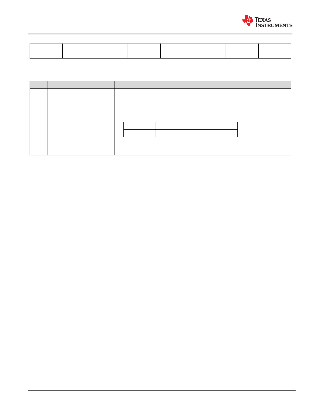
TPS23882
SLVSF21D – AUGUST 2019 – REVISED AUGUST 2020
Figure 9-49. CHANNEL 4 VOLTAGE Register Format (continued)
– – V4_13 V4_12 V4_11 V4_10 V4_9 V4_8
R-0 R-0 R-0 R-0 R-0 R-0 R-0 R-0
LEGEND: R/W = Read/Write; R = Read only; -n = value after reset
Table 9-46. CHANNEL n VOLTAGE Register Field Descriptions
Bit Field Type Reset Description
13-0 Vn_13- Vn_0 R 0 Bit Descriptions: Data conversion result. The I2C data transmission is a 2-byte transfer.
The equation defining the voltage measured is:
V = N × V
Where V
STEP
is defined below as well as the full scale value:
STEP
www.ti.com
Mode Full Scale Value V
STEP
Powered 60 V 3.662 mV
Note that a powered voltage measurement is made between VPWR and DRAINn.
Note: if a channel is OFF, the result through I2C interface is automatically 0000.
84 Submit Document Feedback
Copyright © 2020 Texas Instruments Incorporated
Product Folder Links: TPS23882

V
DRAIN
(V)
I
PORT
(A)
0 3 6 9 12 15 18 21 24 27 30 33 36 39 42 45 48 51 54 57
0
0.025
0.05
0.075
0.1
0.125
0.15
0.175
0.2
0.225
0.25
0.275
0.3
0.325
0.35
0.375
0.4
0.425
0.45
0.475
0.5
D201
2xFBn =0, ALTFBn = 0
2xFBn =0, ALTFBn = 1
V
DRAIN
(V)
I
PORT
(A)
0 3 6 9 12 15 18 21 24 27 30 33 36 39 42 45 48 51 54 57
0
0.1
0.2
0.3
0.4
0.5
0.6
0.7
0.8
0.9
1
1.1
1.2
1.3
D202
2xFBn =1, ALTFBn = 0
2xFBn =1, ALTFBn = 1
www.ti.com
SLVSF21D – AUGUST 2019 – REVISED AUGUST 2020
9.6.2.45 2x FOLDBACK SELECTION Register
COMMAND = 40h with1 Data Byte Read/Write
Figure 9-50. 2x FOLDBACK SELECTION Register Format
7 6 5 4 3 2 1 0
2xFB4 2xFB3 2xFB2 2xFB1 MPOL4 MPOL3 MPOL2 MPOL1
R/W-0 R/W-0 R/W-0 R/W-0 R/W -0 R/W -0 R/W -0 R/W -0
LEGEND: R/W = Read/Write; R = Read only; -n = value after reset
Table 9-47. 2x FOLDBACK SELECTION Register Field Descriptions
Bit Field Type Reset Description
7–4 2xFB4- 2xFB1 R/W 0 When set, this activates the 2x Foldback mode for a channel which increases its I
3-0 MPOL4 -
R/W 0 Manual Policing and Foldback configuration bits
MPOL1
I
levels normal settings, as shown in Figure 9-3. Note that the fault timer starts when the
SHORT
I
threshold is exceeded.
LIM
Notes:
1)
At turn on, the inrush current profile is unaffected by these bits, as shown in Figure 9-2.
2) When a 2xFBn bit is deasserted, the t
setting used for the associated channel is always
LIM
the nominal value (approximately 60 ms). If 2xFBn bit is asserted, then t
channel is programmable as defined in the Timing Configuration register (0x16).
3) If the assigned class for a channel is class 4 or above, the 2xFB bit will be automatically
set during turn on.
0 = The internal device firmware automatically adjusts the Policing (P
) and 2xFBn settings
CUT
based on the assigned class during port turn on
1 = The Policing (P
Note: Independent of these settings, the Policing (P
) and 2xFBn settings will not be changed during port turn on.
CUT
) and 2xFBn settings are returned to
CUT
their default values upon port turn off.
Note: Setting either bit for a 4P configured port disables the automatic configuration on both
channels
The MPOLn bits are cleared upon port turn off.
TPS23882
and
LIM
for associated
LIM
Refer to register 0x55h description for more information on additional Foldback and Inrush
configuration options
Figure 9-51. 1x Mode (2xFBn = 0) Foldback Curves,
I
vs V
PORT
Copyright © 2020 Texas Instruments Incorporated
DRAIN
Note
Figure 9-52. 2x Mode (2xFBn = 1) Foldback Curves,
I
vs V
PORT
Product Folder Links: TPS23882
DRAIN
Submit Document Feedback
85

TPS23882
SLVSF21D – AUGUST 2019 – REVISED AUGUST 2020
www.ti.com
9.6.2.46 FIRMWARE REVISION Register
COMMAND = 41h with 1 Data Byte, Read Only
Figure 9-53. FIRMWARE REVISION Register Format
7 6 5 4 3 2 1 0
FRV
LEGEND: R/W = Read/Write; R = Read only; -n = value after reset
Table 9-48. FIRMWARE REVISION Register Field Descriptions
Bit Field Type Reset Description
7–0 FRV R Firmware Revision number
After a RESET or POR fault this value will default to 0000, 0000b, but upon a “valid” SRAM load, this value will
reflect the corresponding SRAM version of firmware (0x01h – 0xFEh).
Note
If the value of this register = 0xFFh, the device is running in “safe mode”, and the SRAM needs to be
reprogrammed to resume normal operation.
86 Submit Document Feedback
Copyright © 2020 Texas Instruments Incorporated
Product Folder Links: TPS23882

www.ti.com
SLVSF21D – AUGUST 2019 – REVISED AUGUST 2020
9.6.2.47 I2C WATCHDOG Register
COMMAND = 42h with 1 Data Byte, Read/Write
The I2C watchdog timer monitors the I2C clock line in order to prevent hung software situations that could leave
ports in a hazardous state. The timer can be reset by either edge on SCL input. If the watchdog timer expires, all
channels will be turned off and WDS bit will be set. The nominal watchdog time-out period is 2 seconds.
Figure 9-54. I2C WATCHDOG Register Format
TPS23882
7 6 5 4 3 2 1 0
– – – IWDD3 IWDD2 IWDD1 IWDD0 WDS
– – – R/W-1 R/W-0 R/W-1 R/W-1 R/W-0
LEGEND: R/W = Read/Write; R = Read only; -n = value after reset
Table 9-49. I2C WATCHDOG Register Field Descriptions
Bit Field Type Reset Description
4–1 IWDD3–IWDD0 R/W 1011b
0 WDS R/W 0 I2C Watchdog timer status, valid even if the watchdog is masked. When set, it means that
I2C Watchdog disable. When equal to 1011b, the watchdog is masked. Otherwise, it is
umasked and the watchdog is operational.
the watchdog timer has expired without any activity on I2C clock line. Writing 0 at WDS
location clears it.
Note that when the watchdog timer expires and if the watchdog is unmasked, all channels
are also turned off.
When the channels are turned OFF due to I2C watchdog, the corresponding bits are also cleared:
Table 9-50. I2C WATCHDOG Reset
Register Bits to be Reset
0x04 CLSCn and DETCn
0x06 DISFn and PCUTn
0x08 STRTn and ILIMn
0x0C-0F Requested Class and Detection
0x10 PGn and PEn
0x14 CLEn and DETEn
0x1C ACn
0x1E-21 2P Policing set to 0xFFh
0x24 PFn
0x30-3F Channel Voltage and Current Measurements
0x40 2xFBn
0x44 - 47 Detection Resistance Measurements
0x4C-4F Assigned Class and Previous Class
0x51-54 Autoclass Measurement
The corresponding PGCn and PECn bits of Power Event register will also be set if there is a change. The
corresponding PEn and PGn bits of Power Status Register are also updated accordingly.
Note
If the I2C watchdog timer has expired, the Temperature and Input voltage registers will stop being
updated until the WDS bit is cleared. The WDS bit must then be cleared to allow these registers to
work normally.
Copyright © 2020 Texas Instruments Incorporated
Product Folder Links: TPS23882
Submit Document Feedback
87

TPS23882
SLVSF21D – AUGUST 2019 – REVISED AUGUST 2020
9.6.2.48 DEVICE ID Register
COMMAND = 43h with 1 Data Byte, Read Only
Figure 9-55. DEVICE ID Register Format
7 6 5 4 3 2 1 0
DID SR
LEGEND: R/W = Read/Write; R = Read only; -n = value after reset
Table 9-51. DEVICE ID Register Field Descriptions
Bit Field Type Reset Description
7–5 DID R 0011b Device ID number
4–0 SR R 0011b Silicon Revision number
www.ti.com
88 Submit Document Feedback
Copyright © 2020 Texas Instruments Incorporated
Product Folder Links: TPS23882

www.ti.com
SLVSF21D – AUGUST 2019 – REVISED AUGUST 2020
9.6.2.49 CHANNEL 1 DETECT RESISTANCE Register
COMMAND = 44h with 1 Data Byte, Read Only
Figure 9-56. CHANNEL 1 DETECT RESISTANCE Register Format
7 6 5 4 3 2 1 0
R1_7 R1_6 R1_5 R1_4 R1_3 R1_2 R1_1 R1_0
R-0 R-0 R-0 R-0 R-0 R-0 R-0 R-0
LEGEND: R/W = Read/Write; R = Read only; -n = value after reset
9.6.2.50 CHANNEL 2 DETECT RESISTANCE Register
COMMAND = 45h with 1 Data Byte, Read Only
Figure 9-57. CHANNEL 2 DETECT RESISTANCE Register Format
7 6 5 4 3 2 1 0
R2_7 R2_6 R2_5 R2_4 R2_3 R2_2 R2_1 R2_0
R-0 R-0 R-0 R-0 R-0 R-0 R-0 R-0
LEGEND: R/W = Read/Write; R = Read only; -n = value after reset
9.6.2.51 CHANNEL 3 DETECT RESISTANCE Register
TPS23882
COMMAND = 46h with 1 Data Byte, Read Only
Figure 9-58. CHANNEL 3 DETECT RESISTANCE Register Format
7 6 5 4 3 2 1 0
R3_7 R3_6 R3_5 R3_4 R3_3 R3_2 R3_1 R3_0
R-0 R-0 R-0 R-0 R-0 R-0 R-0 R-0
LEGEND: R/W = Read/Write; R = Read only; -n = value after reset
9.6.2.52 CHANNEL 4 DETECT RESISTANCE Register
COMMAND = 47h with 1 Data Byte, Read Only
Figure 9-59. CHANNEL 4 DETECT RESISTANCE Register Format
7 6 5 4 3 2 1 0
R4_7 R4_6 R4_5 R4_4 R4_3 R4_2 R4_1 R4_0
R-0 R-0 R-0 R-0 R-0 R-0 R-0 R-0
LEGEND: R/W = Read/Write; R = Read only; -n = value after reset
Table 9-52. DETECT RESISTANCE Register Fields Descriptions
Bit Field Type Reset Description
7-0 Rn_7- Rn_0 R 0 8-bit data conversion result of detection resistance for channel n.
Most recent 2-point Detection Resistance measurement result. The I2C data transmission is a 1-byte transfer.
Note that the register content is not cleared at turn off.
The equation defining the resistance measured is:
R = N × R
Where R
STEP
is defined below as well as the full scale value:
STEP
Copyright © 2020 Texas Instruments Incorporated
Useable Resistance Range R
2 kΩ to 50 kΩ 195.3125 Ω
Product Folder Links: TPS23882
STEP
Submit Document Feedback
89

TPS23882
SLVSF21D – AUGUST 2019 – REVISED AUGUST 2020
9.6.2.53 CHANNEL 1 DETECT CAPACITANCE Register
COMMAND = 48h with 1 Data Byte, Read Only
Figure 9-60. CHANNEL 1 DETECT CAPACITANCE Register Format
7 6 5 4 3 2 1 0
C1_7 C1_6 C1_5 C1_4 C1_3 C1_2 C1_1 C1_0
R-0 R-0 R-0 R-0 R-0 R-0 R-0 R-0
LEGEND: R/W = Read/Write; R = Read only; -n = value after reset
9.6.2.54 CHANNEL 2 DETECT CAPACITANCE Register
COMMAND = 49h with 1 Data Byte, Read Only
Figure 9-61. CHANNEL 2 DETECT CAPACITANCE Register Format
7 6 5 4 3 2 1 0
C2_7 C2_6 C2_5 C2_4 C2_3 C2_2 C2_1 C2_0
R-0 R-0 R-0 R-0 R-0 R-0 R-0 R-0
LEGEND: R/W = Read/Write; R = Read only; -n = value after reset
9.6.2.55 CHANNEL 3 DETECT CAPACITANCE Register
www.ti.com
COMMAND = 4Ah with 1 Data Byte, Read Only
Figure 9-62. CHANNEL 3 DETECT CAPACITANCE Register Format
7 6 5 4 3 2 1 0
C3_7 C3_6 C3_5 C3_4 C3_3 C3_2 C3_1 C3_0
R-0 R-0 R-0 R-0 R-0 R-0 R-0 R-0
LEGEND: R/W = Read/Write; R = Read only; -n = value after reset
9.6.2.56 CHANNEL 4 DETECT CAPACITANCE Register
COMMAND = 4Bh with 1 Data Byte, Read Only
Figure 9-63. CHANNEL 4 DETECT CAPACITANCE Register Format
7 6 5 4 3 2 1 0
C4_7 C4_6 C4_5 C4_4 C4_3 R4_2C C4_1 C4_0
R-0 R-0 R-0 R-0 R-0 R-0 R-0 R-0
LEGEND: R/W = Read/Write; R = Read only; -n = value after reset
90 Submit Document Feedback
Copyright © 2020 Texas Instruments Incorporated
Product Folder Links: TPS23882

www.ti.com
SLVSF21D – AUGUST 2019 – REVISED AUGUST 2020
Table 9-53. DETECT CAPACITANCE Register Fields Descriptions
Bit Field Type Reset Description
7-0 Cn_7- Cn_0 R 0 8-bit data conversion result of capacitance measurement for channel n.
Most recent capacitance measurement result. The I2C data transmission is a 1-byte transfer.
The equation defining the resistance measured is:
C = N × C
Where C
STEP
is defined below as well as the full scale value:
STEP
TPS23882
Useable Resistance Range C
STEP
1 µF to 12 µF 0.05 µF
Note that the register content is not cleared at turn off.
Note: The capacitance measurement is only supported in Manual/Diagnostic mode.
Note: No capacitance measurement will be made if the result of the resistance detection is
returned as "valid".
Note: The TPS23882 SRAM needs to be programmed in order for the capacitance
measurement to operate properly.
Copyright © 2020 Texas Instruments Incorporated
Product Folder Links: TPS23882
Submit Document Feedback
91

TPS23882
SLVSF21D – AUGUST 2019 – REVISED AUGUST 2020
9.6.2.57 CHANNEL 1 ASSIGNED CLASS Register
COMMAND = 4Ch with 1 Data Byte, Read Only
Figure 9-64. CHANNEL 1 ASSIGNED CLASS Register Format
7 6 5 4 3 2 1 0
ACLASS Ch1 PCLASS Ch1
R-0 R-0 R-0 R-0 R-0 R-0 R-0 R-0
LEGEND: R/W = Read/Write; R = Read only; -n = value after reset
9.6.2.58 CHANNEL 2 ASSIGNED CLASS Register
COMMAND = 4Dh with 1 Data Byte, Read Only
Figure 9-65. CHANNEL 2 ASSIGNED CLASS Register Format
7 6 5 4 3 2 1 0
ACLASS Ch2 PCLASS Ch2
R-0 R-0 R-0 R-0 R-0 R-0 R-0 R-0
LEGEND: R/W = Read/Write; R = Read only; -n = value after reset
9.6.2.59 CHANNEL 3 ASSIGNED CLASS Register
www.ti.com
COMMAND = 4Eh with 1 Data Byte, Read Only
Figure 9-66. CHANNEL 3 ASSIGNED CLASS Register Format
7 6 5 4 3 2 1 0
ACLASS Ch3 PCLASS Ch3
R-0 R-0 R-0 R-0 R-0 R-0 R-0 R-0
LEGEND: R/W = Read/Write; R = Read only; -n = value after reset
9.6.2.60 CHANNEL 4 ASSIGNED CLASS Register
COMMAND = 4Fh with 1 Data Byte, Read Only
Figure 9-67. CHANNEL 4 ASSIGNED CLASS Register Format
7 6 5 4 3 2 1 0
ACLASS Ch4 PCLASS Ch4
R-0 R-0 R-0 R-0 R-0 R-0 R-0 R-0
LEGEND: R/W = Read/Write; R = Read only; -n = value after reset
Bit Descriptions: These bits represent the "assigned" and previous classification results for channel n. These
bits are cleared when channel n is turned off.
92 Submit Document Feedback
Copyright © 2020 Texas Instruments Incorporated
Product Folder Links: TPS23882

www.ti.com
Table 9-54. CHANNEL n ASSIGNED CLASS Register Field Descriptions
Bit Field Type Reset Description
7–4 ACLASS
Ch-n
3–0 PCLASS
Ch-n
R 0 Assigned classification on channel n.
See Table 9-55 below
R 0 Previous Class result on channel n.
See Table 9-56 below
Table 9-55. Assigned Class Designations
ACLASS-Chn Assigned Class
Bit 7 Bit 6 Bit 5 Bit 4
0 0 0 0 Unknown
0 0 0 1 Class 1
0 0 1 0 Class 2
0 0 1 1 Class 3
0 1 0 0 Class 4
0 1 0 1 Reserved
0 1 1 0 Reserved
0 1 1 1 Reserved
1 X X X Reserved
SLVSF21D – AUGUST 2019 – REVISED AUGUST 2020
TPS23882
Table 9-56. Previous Class Designations
PCLASS-Chn Previous Class
Bit 7 Bit 6 Bit 5 Bit 4
0 0 0 0 Unknown
0 0 0 1 Class 1
0 0 1 0 Class 2
0 0 1 1 Class 3
0 1 0 0 Class 4
0 1 0 1 Reserved
0 1 1 0 Class 0
0 1 1 1 Reserved
1 0 0 0 Class 5 - 4-Pair
1 0 0 1 Class 6 - 4-Pair
1 0 1 0 Class 7 - 4-Pair
1 0 1 1 Class 8 - 4-Pair
1 1 X X Reserved
Copyright © 2020 Texas Instruments Incorporated
Product Folder Links: TPS23882
Submit Document Feedback
93

TPS23882
SLVSF21D – AUGUST 2019 – REVISED AUGUST 2020
www.ti.com
“Requested” vs. “Assigned” Classification:
The “requested” class is the classification the PSE measures during Mutual Identification prior to turn on,
whereas the “assigned” class is the classification level the Channel was powered on with based on the Power
Allocation setting in register 0x29h. The “requested” classification values are available in registers 0x0C-0F
Note
Upon being powered, devices that present a class 0 signature during discovery will be given an
assigned class of "Class 3"
Note
There is no Assigned Class assigned for ports/channels powered out of Manual/Diagnostic mode. Any
settings such as the port power policing and 1x/2x foldback selection that are typically configure based
on the assigned class result need to manually configured by the user.
Previous Classification
In certain circumstances the requested class result in 0x0C-0F can not properly reflect the actual classification of
the PD connected to the port/channel. This will happen when a port has a power allocation limit of 15.4W and
the PSE can only provide 1 classification finger during turn on. When this occurs and if the device is configured
to run in Semi Auto mode with det and cls enabled, the 3-finger classification measurement that preceded the
turn on detection and classification cycle will be stored here. This information can be useful in scenarios where a
port had to be demoted to stay under the system power limit at turn on but additional power budget comes
available later on.
Note
The Previous Classification results are only valid for channels being used in semi auto mode with
ongoing discovery (DETE and CLE = 1).
94 Submit Document Feedback
Copyright © 2020 Texas Instruments Incorporated
Product Folder Links: TPS23882

www.ti.com
SLVSF21D – AUGUST 2019 – REVISED AUGUST 2020
9.6.2.61 AUTO CLASS CONTROL Register
COMMAND = 50h with 1 Data Byte, Read/Write
Figure 9-68. AUTO CLASS CONTROL Register Format
7 6 5 4 3 2 1 0
MAC4 MAC3 MAC2 MAC1 AAC4 AAC3 AAC2 AAC1
R/W-0 R/W-0 R/W-0 R/W-0 R/W-0 R/W-0 R/W-0 R/W-0
LEGEND: R/W = Read/Write; R = Read only; -n = value after reset
Table 9-57. AUTO CLASS CONTROL Register Field Descriptions
Bit Field Type Reset Description
7 - 4 MACn R/W 0 Manual Auto Class Measurement bits
1 = Manual Auto Class Measurement enabled
0 = Manual Auto Class measurement complete
The auto class measurement will begin within 10ms of this bit being set.
This bit will be cleared by the internal firmware within 1ms of the updated Autoclass
measurement result(s) in 0x51-54h.
3 -0 AACn R/W 0 Auto Class Auto Adjustment Enable bits
1 = Autoclass auto adjust is enabled and the corresponding PCUT settings will be
automatically adjusted based on the measured autoclass power
0 = Autoclass auto adjust is disabled and it is up to the user to adjust the value of PCUT as
desired.
TPS23882
SPACE
Note
Any MACn bits set prior to turn on will be ignored and cleared during turn on.
Auto Class Pcut Adjustments:
If the ACx bit(s) are set in register 0x50h, the TPS23882 will automatically adjust its PCUT value based on the
auto class power measurement (PAC in registers 0x51-54) and Any Automatic Auto Class facilitated (AACn = 1)
PCut adjustments will be made within 5 ms of the end of the auto class measurement period.
SPACE
Copyright © 2020 Texas Instruments Incorporated
Product Folder Links: TPS23882
Submit Document Feedback
95

TPS23882
SLVSF21D – AUGUST 2019 – REVISED AUGUST 2020
9.6.2.62 CHANNEL 1 AUTO CLASS POWER Register
COMMAND = 51h with 1 Data Byte, Read Only
Figure 9-69. CHANNEL 1 AUTO CLASS POWER Register Format
7 6 5 4 3 2 1 0
- PAC1_6 PAC1_5 PAC1_4 PAC1_3 PAC1_2 PAC1_1 PAC1_0
R-0 R-0 R-0 R-0 R-0 R-0 R-0 R-0
LEGEND: R/W = Read/Write; R = Read only; -n = value after reset
9.6.2.63 CHANNEL 2 AUTO CLASS POWER Register
COMMAND = 52h with 1 Data Byte, Read Only
Figure 9-70. CHANNEL 2 AUTO CLASS POWER Register Format
7 6 5 4 3 2 1 0
- PAC2_6 PAC2_5 PAC2_4 PAC2_3 PAC2_2 PAC2_1 PAC2_0
R-0 R-0 R-0 R-0 R-0 R-0 R-0 R-0
LEGEND: R/W = Read/Write; R = Read only; -n = value after reset
9.6.2.64 CHANNEL 3 AUTO CLASS POWER Register
www.ti.com
COMMAND = 53h with 1 Data Byte, Read Only
Figure 9-71. CHANNEL 3 AUTO CLASS POWER Register Format
7 6 5 4 3 2 1 0
- PAC3_6 PAC3_5 PAC3_4 PAC3_3 PAC3_2 PAC3_1 PAC3_0
R-0 R-0 R-0 R-0 R-0 R-0 R-0 R-0
LEGEND: R/W = Read/Write; R = Read only; -n = value after reset
9.6.2.65 CHANNEL 4 AUTO CLASS POWER Register
COMMAND = 54h with 1 Data Byte, Read Only
Figure 9-72. CHANNEL 4 AUTO CLASS POWER Register Format
7 6 5 4 3 2 1 0
- PAC4_6 PAC4_5 PAC4_4 PAC4_3 PAC4_2 PAC4_1 PAC4_0
R-0 R-0 R-0 R-0 R-0 R-0 R-0 R-0
LEGEND: R/W = Read/Write; R = Read only; -n = value after reset
Table 9-58. AUTO CLASS POWER Register Fields Descriptions
Bit Field Type Reset Description
6-0 PACn_6-
PACn_0
R 0 8-bit data conversion result of the auto class power measurement for channel n.
Peak average power calculation result from channel voltage and current data conversion
measurements taken during the auto class power measurement window.
The equation defining the auto class power measured is:
PAC= N × P
Where, when assuming 0.200-Ω Rsense resistor is used:
PC
STEP
AC_STEP
= 0.5 W
SPACE
96 Submit Document Feedback
Copyright © 2020 Texas Instruments Incorporated
Product Folder Links: TPS23882

V
DRAIN
(V)
I
PORT
(A)
0 3 6 9 12 15 18 21 24 27 30 33 36 39 42 45 48 51 54 57
0
0.025
0.05
0.075
0.1
0.125
0.15
0.175
0.2
0.225
0.25
0.275
0.3
0.325
0.35
0.375
0.4
0.425
0.45
0.475
0.5
D201
2xFBn =0, ALTFBn = 0
2xFBn =0, ALTFBn = 1
V
DRAIN
(V)
I
PORT
(A)
0 3 6 9 12 15 18 21 24 27 30 33 36 39 42 45 48 51 54 57
0
0.1
0.2
0.3
0.4
0.5
0.6
0.7
0.8
0.9
1
1.1
1.2
1.3
D202
2xFBn =1, ALTFBn = 0
2xFBn =1, ALTFBn = 1
V
PORT
(V)
I
PORT
(A)
0 3 6 9 12 15 18 21 24 27 30 33 36 39 42 45 48 51 54 57
0
0.05
0.1
0.15
0.2
0.25
0.3
0.35
0.4
0.45
0.5
0.55
D100
ALTIRn = 0
ALTIRn = 1
www.ti.com
SLVSF21D – AUGUST 2019 – REVISED AUGUST 2020
9.6.2.66 ALTERNATIVE FOLDBACK Register
COMMAND = 55h with 1 Data Byte, Read/Write
Figure 9-73. ALTERNATIVE FOLDBACK Register Format
7 6 5 4 3 2 1 0
ALTFB4 ALTFB3 ALTFB2 ALTFB1 ALTIR4 ALTIR3 ALTIR2 ALTIR1
R/W-0 R/W-0 R/W-0 R/W-0 R/W-0 R/W-0 R/W-0 R/W-0
LEGEND: R/W = Read/Write; R = Read only; -n = value after reset
Table 9-59. ALTERNATIVE FOLDBACK Register Field Descriptions
Bit Field Type Reset Description
7-4 ALTFBn R 0 Alternative Foldback Enable bits: Used to enable the operational alterative foldback curves while powered.
1 = Alternative Foldback is enabled
0 = Alternative Foldback is disabled
The ALTFBn bits should be set prior to issuing a PWONn command to ensure the desired foldback curve is
being used.
3-0 ALTIRn R 0 Alternative Inrush Enable bits: Used to enable the alterative foldback curves during inrush on channel n
1 = Alternative Inrush is enabled
0 = Alternative Inrush is disabled
Note: The ALTIRn bits need to be set prior to sending a PWONn command to ensure the desired inrush
behavior is followed
TPS23882
SPACE
Figure 9-74. 1x Mode (2xFBn = 0) Foldback Curves,
I
vs V
PORT
DRAIN
Figure 9-75. 2x Mode (2xFBn = 1) Foldback Curves,
I
vs V
PORT
DRAIN
Copyright © 2020 Texas Instruments Incorporated
Figure 9-76. Inrush Foldback Curves, I
Product Folder Links: TPS23882
PORT
vs V
PORT
Submit Document Feedback
97

TPS23882
SLVSF21D – AUGUST 2019 – REVISED AUGUST 2020
9.6.2.67 SRAM CONTROL Register
COMMAND = 60h with 1 Data Byte, Read/Write
Figure 9-77. SRAM CONTROL Register Format
7 6 5 4 3 2 1 0
PROG_SEL CPU_RST - PAR_EN RAM_EN PAR_SEL R/WZ CLR_PTR
R/W-0 R/W-0 R/W-0 R/W-0 R/W-0 R/W-0 R/W-0 R/W-0
LEGEND: R/W = Read/Write; R = Read only; -n = value after reset
Table 9-60. SRAM CONTROL Register Field Descriptions
Bit Field Type Reset Description
7 PROG_SEL R/W 0 I2C Programming select bit.
1 = SRAM I2C read/write is enabled
0 = SRAM I2C read/write is disabled.
6 CPU_RST R/W 0 CPU Reset bit
1 = Internal CPU is held in RESET
0 = Internal CPU is active
This is strictly a CPU reset. Toggling this bit reset the cpu only and will not change any
contents of the I2C registers
5 Reserved R/W 0 Reserved
4 PAR_EN R/W 0 SRAM Parity Enable bit:
1 = SRAM Parity Check will be enabled
0 = SRAM Parity Check will be disabled
It is recommended that the Parity function be enable whenever SRAM is being used
3 RAM_EN R/W 0 SRAM Enable bit
1 = SRAM will be enabled and the internal CPU will run from both SRAM and internal ROM
0 = Internal CPU will run from internal ROM only
This bit needs to be set to a 1 after SRAM programing to enable the utilization of the SRAM
code
2 PAR_SEL R/W 0 SRAM Parity Select bit: Setting this bit to a 1 in conjunction with the RZ/W bit enables
access to the SRAM Parity bits.
1 = Parity bits read/write is enabled
0 = Parity bits read/write is disabled
1 R/WZ R/W 0 SRAM Read/Write select bit:
0 = SRAM Write – SRAM data is written with a write to 0x61h
1 = SRAM Read – SRAM data is read with a read from 0x61h
SRAM data can be continuously read/written over I2C until a STOP bit is sent.
0 CLR_PTR R/W 0 Clear Address Pointer bit:
1 = Resets the memory address pointer
0 = Releases pointer for use
In order to ensure proper programming, this bit should be toggled (0-1-0) to writing or
reading the SRAM or Parity memory.
www.ti.com
98 Submit Document Feedback
Copyright © 2020 Texas Instruments Incorporated
Product Folder Links: TPS23882

www.ti.com
SLVSF21D – AUGUST 2019 – REVISED AUGUST 2020
9.6.2.67.1 SRAM START ADDRESS (LSB) Register
COMMAND = 62h with 1 Byte, Read/Write
Figure 9-78. SRAM START ADDRESS (LSB) Register Format
7 6 5 4 3 2 1 0
SA_7 SA_6 SA_5 SA_4 SA_3 SA_2 SA_1 SA_0
R/W-0 R/W-0 R/W-0 R/W-0 R/W-0 R/W-0 R/W-0 R/W-0
LEGEND: R/W = Read/Write; R = Read only; -n = value after reset
9.6.2.67.2 SRAM START ADDRESS (MSB) Register
COMMAND = 63h with 1 Byte, Read/Write
Figure 9-79. SRAM START ADDRESS (MSB) Register Format
7 6 5 4 3 2 1 0
SA_15 SA_14 SA_13 SA_12 SA_11 SA_10 SA_9 SA_8
R/W-0 R/W-0 R/W-0 R/W-0 R/W-0 R/W-0 R/W-0 R/W-0
LEGEND: R/W = Read/Write; R = Read only; -n = value after reset
9.6.2.67.3
TPS23882
Table 9-61. SRAM START ADDRESS Register Field Descriptions
Bit Field Type Reset Description
15-0 SA_15- SA_0 R/W 0 SRAM and Parity Programing Start Address bits:
the value entered into these registers sets the start address location for the SRAM or Parity
programming
Copyright © 2020 Texas Instruments Incorporated
Product Folder Links: TPS23882
Submit Document Feedback
99

TPS23882
SLVSF21D – AUGUST 2019 – REVISED AUGUST 2020
www.ti.com
SRAM Programming:
Upon power up, it is recommended that the TPS23882 device's SRAM be programmed with the latest version of
SRAM code via the I2C to ensure proper operation and IEEE complaint performance. All I2C traffic other than
those commands required to program the SRAM should be deferred until after the SRAM programming
sequences are completed.
Note
The latest version of firmware and SRAM release notes may be accessed from the TI mySecure
Software webpage.
The SRAM Release Notes and ROM Advisory document includes more detailed information regarding
any know issues and changes that were associated with each firmware release.
Note
The SRAM programming control must be completed at the lower I2C address (Channels 1-4, A0 = 0).
Configuring this registers for the upper I2C device address (Channels 5-8) will not program the SRAM
For systems that include multiple TPS23882 devices, the 0x7F "global" broadcast I2C address may be
used to programmed all of the devices at the same time.
Note
The SRAM programming needs to be delayed at least 50ms from the initial power on (VPWR and
VDD above UVLO) of the device to allow for the device to complete its internal hardware initialization
process
Note
For more detailed instructions on the SRAM programing procedures please refer the How to Load
TPS2388x SRAM Code document on TI.com.
SPACE
0x60h setup for SRAM Programming: Prior to programming/writing the SRAM, the following bits sequence
needs to be completed in register 0x60h:
7
PROG_SEL CPU_RST - PAR_EN RAM_EN PAR_SEL R/WZ CLR_PTR
0 → 1 0 → 1 0 0 0 0 1 → 0 0 → 1 → 0
6 5 4 3 2 1 0
The same sequence is required to read the SRAM with the exception that the R/WZ bit needs to be set to “1”.
If the device is in “Safe Mode”, the same sequence as above may be used to reprogram the SRAM.
An I2C write to 0x61h following this sequence actively programs the SRAM program memory starting from the
address set in registers 0x62h and 63h.
100 Submit Document Feedback
Copyright © 2020 Texas Instruments Incorporated
Product Folder Links: TPS23882
 Loading...