

Page 1
TPS23753
M1
R
CS
C
OUT
D
VC
GATE
RTN
V
C
CS
C
VC
CTL
V
B
D1
58V
C1
0.1µF
R
DEN
R
CLS
From Ethernet
Transformers
V
DD1
V
SS
CLS
C
IN
V
OUT
R
CTL
C
CTL
From Spare
Pairs or
Transformers
D
S
DEN
BLNK
FRS
D
A
R
FRS
V
B
C
VB
Adapter
R
FBU
R
FBL
TLV431
R
OB
C
IZ
APD
R
APD2
R
APD1
R
BLNK
V
DD
C
IO
T1
BR1
BR2
R
VC
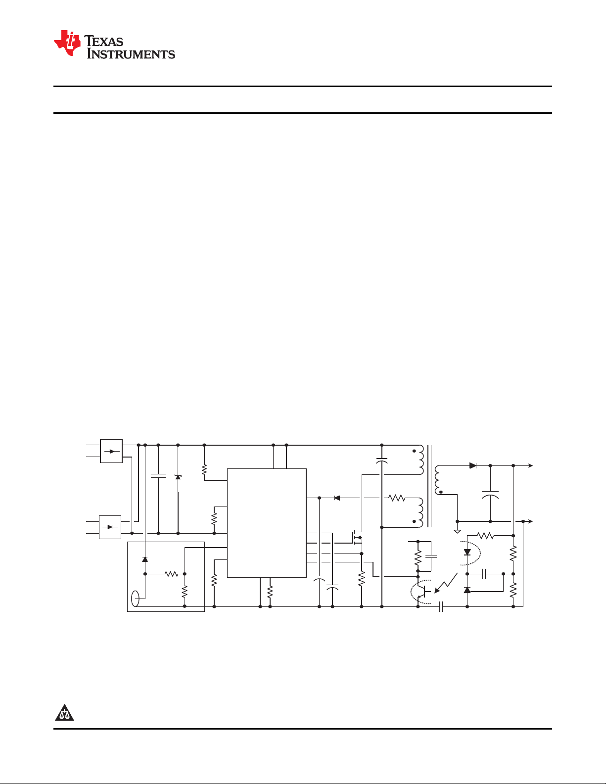
* AdapterinterfaceandR
BLNK
areOptional
*
*
TPS23753
www.ti.com
.............................................................................................................................................................. SLVS853A – JUNE 2008 – REVISED JUNE 2008
IEEE 802.3-2005 PoE INTERFACE AND ISOLATED CONVERTER CONTROLLER
1
FEATURES
• Optimized for Isolated Converters
• Complete PoE Interface
• Adapter ORing Support
• 12 V Adapter Support
• Programmable Frequency with Synch.
• Robust 100 V, 0.7 Ω Hotswap MOSFET
• Small TSSOP 14 Package
• 15 kV / 8 kV System Level ESD Capable
• – 40 ° C to 125 ° C Junction Temperature Range
• Design Procedure Application Note - SLVA305
• Adapter ORing Application Note - SLVA306
APPLICATIONS
• IEEE 802.3-2005 Compliant Powered Devices
• VoIP Telephones
• Access Points
• Security Cameras
DESCRIPTION
The TPS23753 is a combined Power over Ethernet
(PoE) powered device (PD) interface and
current-mode dc/dc controller optimized specifically
for isolated converter designs. The PoE
implementation supports the IEEE 802.3-2005
(previously 802.3af) standard, 12.95 W (13 W) PD.
The TPS23753 supports a number of input-voltage
ORing options including highest voltage, external
adapter preference, and PoE preference.
The PoE interface features an external detection
signature pin that can also be used to disable the
internal hotswap MOSFET. This allows the PoE
function to be turned off. Classification can be
programmed to any of the defined types with a single
resistor.
The dc/dc controller features a bootstrap startup
mechanism with an internal, switched current source.
This provides the advantages of cycling overload fault
protection without the constant power loss of a pull up
resistor.
The programmable oscillator may be synchronized to
a higher-frequency external timing reference.
1
PRODUCTION DATA information is current as of publication date.
Products conform to specifications per the terms of the Texas
Instruments standard warranty. Production processing does not
necessarily include testing of all parameters.
Please be aware that an important notice concerning availability, standard warranty, and use in critical applications of Texas
Instruments semiconductor products and disclaimers thereto appears at the end of this data sheet.
Figure 1. Basic TPS23753 Implementation
Copyright © 2008, Texas Instruments Incorporated
Page 2
TPS23753
SLVS853A – JUNE 2008 – REVISED JUNE 2008 ..............................................................................................................................................................
www.ti.com
This device contains circuits to protect its inputs and outputs against damage due to high static voltages or electrostatic fields.
These circuits have been qualified to protect this device against electrostatic discharges (ESD) of up to 2 kV according to
MIL-STD-883C, Method 3015; however, it is advised that precautions be taken to avoid application of any voltage higher than
maximum-rated voltages to these high-impedance circuits. During storage or handling the device leads should be shorted together
or the device should be placed in conductive foam. In a circuit, unused inputs should always be connected to an appropriate logic
voltage level, preferably either V
Guidelines for Handling Electrostatic-Discharge-Sensitive (ESDS) Devices and Assemblies available from Texas Instruments.
or ground. Specific guidelines for handling devices of this type are contained in the publication
CC
PRODUCT INFORMATION
(1)
DEVICE DUTY CYCLE POE UVLO ON / HYST. PACKAGE MARKING
TPS23753 0 – 80% 35/4.5 PW (TSSOP-14) TP23753
(1) For the most current package and ordering information, see the Package Option Addendum at the end of this document, or see the TI
website at www.ti.com .
ABSOLUTE MAXIMUM RATINGS
Voltags are with respect to V
(unless otherwise noted)
SS
(1)
VALUE UNIT
V
Input voltage range [APD, BLNK
I
VDD, V
V
CLS
DD1
, DEN, RTN
DD1
to RTN – 0.3 to 100 V
(3)
(3)
CS to RTN – 0.3 to V
, CTL, FRS
(2)
– 0.3 to 100 V
– 0.3 to 6.5 V
(3)
(3)
, V
] to RTN – 0.3 to 6.5 V
B
B
VCto RTN – 0.3 to 19 V
GATE to RTN – 0.3 to VC+ 0.3 V
Sourcing current V
B
Internally limited mA
Average sourcing or sinking current GATE 25 mA
ESD rating
ESD – system level (contact/air)
T
Operating junction temperature range ° C
J
(4)
HBM 2 kV
CDM 500 V
8/15 kV
– 40 to Internally
Limited
(1) Stresses beyond those listed under absolute maximum ratings may cause permanent damage to the device. These are stress ratings
only, and functional operation of the device at these or any other conditions beyond those indicated under recommended operating
conditions is not implied. Exposure to absolute-maximum-rated conditions for extended periods may affect device reliability.
(2) I
(3) Do not apply voltage to these pins.
= 0 for V
RTN
> 80V.
RTN
(4) Surges per EN61000-4-2, 1999 applied between RJ-45 and output ground and between adapter input and output ground of the
TPS23753EVM-001 (HPA304-001) evaluation module (documentation available on the web). These were the test levels, not the failure
threshold.
V
RMS
DISSIPATION RATINGS
θ
PACKAGE
JT
(1)
( ° C/W)
PW (TSSOP-14) 0.97 173.6 99.3
(1) JEDEC method with high-k board (4 layers, 2 signal and 2 planes).
(2) JEDEC method with low-k board (2 signal layers).
2 Submit Documentation Feedback Copyright © 2008, Texas Instruments Incorporated
Product Folder Link(s): TPS23753
θ
JA
(2)
( ° C/W)
θ
JA
(1)
( ° C/W)
Page 3
TPS23753
www.ti.com
.............................................................................................................................................................. SLVS853A – JUNE 2008 – REVISED JUNE 2008
RECOMMENDED OPERATING CONDITIONS
Voltage with respect to V
Input voltage range, VDD, V
Input voltage range, VDD, V
V
I
R
BLNK
T
J
Input voltage range, VCto RTN 0 18 V
Input voltage range, APD, CTL to RTN 0 V
Input voltage range, CS to RTN 0 2 V
RTN current (T
VBsourcing current 0 2.5 5 mA
VBcapacitance 0.08 0.1 2.2 µ F
Synchronization pulse width input (when used) 25 150 ns
Operating junction temperature range – 40 125 ° C
(unless otherwise noted)
SS
, RTN 0 57 V
DD1
to RTN 0 57 V
DD1
≤ 125 ° C) 350 mA
J
ELECTRICAL CHARACTERISTICS
Unless otherwise noted: CS = APD = CTL = RTN, GATE open, R
24.9 k Ω , R
Controller Section Only
[V
= RTN and V
SS
V
C
UVLO
1
UVLO
H
t
ST
V
B
FRS
D
MAX
V
SYNC
CTL
V
ZDC
BLNK
CS
V
CSMAX
t
1
V
SLOPE
I
SL_EX
(1) The hysteresis tolerance tracks the rising threshold for a given device.
open, V
CLS
= V
DD
PARAMETER TEST CONDITIONS MIN TYP MAX UNIT
Undervoltage lockout V
Operating current VC= 12 V, CTL = V
Startup time, CVC= 22 µ F ms
Startup current source - I
Voltage 6.5 V ≤ VC≤ 18 V, 0 ≤ IVB≤ 5 mA 4.75 5.10 5.25 V
Switching frequency 223 248 273 kHz
Duty cycle CTL= VB, Measure GATE 76 78.5 81 %
Synchronization Input threshold 2.0 2.2 2.4 V
0% duty cycle threshold V
Softstart period Interval from switching start to V
Input resistance 70 100 145 k Ω
Blanking delay BLNK = RTN 35 52 75 ns
Maximum threshold voltage V
Turn off delay VCS= 0.65 V 25 41 60 ns
Internal slope compensation voltage Peak voltage at maximum duty cycle, referred to CS 90 118 142 mV
Peak slope compensation current V
Bias current (sourcing) Gate high, dc component of CS current 2 3 4.2 µ A
= 48 V, V
VDD-VSS
] or [V
DD1
= RTN = V
SS
VC
VDD1-RTN
= 48 V, 8.5 V ≤ V
], all voltages referred to RTN. Typical specifications are at 25 ° C.
DD
VCrising 8.65 9 9.3
Hysteresis
V
V
V
V
CTL= VB, Measure GATE
R
In addition to t
R
(1)
= 10.2 V, VC(0) = 0 V 50 85 175
DD1
= 35 V, VC(0) = 0 V 30 48 85
DD1
= 10.2 V, VVC= 8.6 V 0.44 1.06 1.80
DD1
= 48 V, VVC= 0 V 2.5 4.3 6.0
DD1
= 60.4 k Ω
FRS
↓ until GATE stops 1.3 1.5 1.7 V
CTL
1
= 49.9 k Ω 41 52 63
BLNK
= VB, VCS↑ until GATE duty cycle drops 0.50 0.55 0.60 V
CTL
= VB, ICSat maximum duty cycle (ac component) 30 42 54 µ A
CTL
MIN NOM MAX UNIT
B
V
0 350 k Ω
= 60.4 k Ω , R
FRS
≤ 18 V, – 40 ° C ≤ TJ≤ 125 ° C
VC-RTN
B
CSMAX
BLNK
= 249 k Ω , C
= C
VB
= 0.1 µ F, R
VC
3.3 3.5 3.7
0.40 0.58 0.85 mA
400 800 µ s
=
DEN
mA
Copyright © 2008, Texas Instruments Incorporated Submit Documentation Feedback 3
Product Folder Link(s): TPS23753
Page 4
TPS23753
SLVS853A – JUNE 2008 – REVISED JUNE 2008 ..............................................................................................................................................................
www.ti.com
ELECTRICAL CHARACTERISTICS (continued)
Unless otherwise noted: CS = APD = CTL = RTN, GATE open, R
24.9 k Ω , R
open, V
CLS
= 48 V, V
VDD-VSS
VDD1-RTN
= 48 V, 8.5 V ≤ V
Controller Section Only
[V
= RTN and V
SS
GATE
APD
V
APDEN
V
APDH
THERMAL SHUTDOWN
(2) The hysteresis tolerance tracks the rising threshold for a given device.
(3) These parameters are provided for reference only, and do not constitute part of TI ' s published device specifications for purposes of TI ' s
product warranty.
= V
DD
] or [V
DD1
= RTN = V
SS
], all voltages referred to RTN. Typical specifications are at 25 ° C.
DD
PARAMETER TEST CONDITIONS MIN TYP MAX UNIT
Source current V
Sink current V
Threshold voltage V
= VB, VC= 12 V, GATE high, Pulsed measurement 0.30 0.46 0.60 A
CTL
= VB, VC= 12 V, GATE low, Pulsed measurement 0.50 0.79 1.1 A
CTL
V
↑ 1.42 1.5 1.58
APD
Hysteresis
(2)
Turn off temperature 135 145 155 ° C
Hysteresis
(3)
= 60.4 k Ω , R
FRS
≤ 18 V, – 40 ° C ≤ TJ≤ 125 ° C
VC-RTN
BLNK
= 249 k Ω , C
= C
VB
VC
0.28 0.3 0.32
= 0.1 µ F, R
20 ° C
DEN
ELECTRICAL CHARACTERISTICS
PoE and Control
[V
= V
DD
] or [V
DD1
DEN (DETECTION) (V
Detection current VDD= 1.6 V 62 64.3 66.5 µ A
Detection bias current VDD= 10 V, DEN open, Measure I
V
PD_DIS
I
lkg
Hotswap disable threshold 3 4 5 V
DEN leakage current V
CLS (CLASSIFICATION) (V
I
CLS
V
CL_ON
V
CL_HYS
V
CU_OFF
V
CU_HYS
I
lkg
Classification current mA
Classification regulator lower
threshold
Classification regulator upper
threshold
Leakage current VDD= 57 V, V
RTN (PASS DEVICE) (V
On resistance 0.7 1.2 Ω
Current limit V
Inrush limit V
Foldback voltage threshold VDDrising 11 12.3 13.6 V
I
lkg
Leakage current VDD= V
UVLO
UVLO_R VDDrising 33.9 35 36.1
UVLO_H Hysteresis
Undervoltage lockout threshold V
(1) The hysteresis tolerance tracks the rising threshold for a given device.
DD1
] = RTN, V
= 0 V, all voltages referred to V
VC-RTN
. Typical specifications are at 25 ° C.
SS
PARAMETER TEST CONDITIONS MIN TYP MAX UNIT
= V
Measure I
DD1
= RTN = V
DD
SUPPLY
positive)
SUPPLY
VDD= 10 V 399 406 413
SUPPLY
= VDD= 57 V, Float V
DEN
13 V ≤ VDD≤ 21 V, Measure I
R
= 1270 Ω 1.8 2.14 2.4
CLS
R
= 243 Ω 9.9 10.6 11.3
CLS
R
= 137 Ω 17.6 18.6 19.4
CLS
R
= 90.9 Ω 26.5 27.9 29.3
CLS
R
= 63.4 Ω 38 39.9 42
CLS
DD1
= V
DD
DD1
SUPPLY
and RTN, Measure I
= RTN = V
SUPPLY
DEN
positive)
5.2 12 µ A
0.1 5 µ A
Regulator turns on, VDDrising 10 11.7 13
Hysteresis
(1)
1.9 2.05 2.2
Regulator turns off, VDDrising 21 22 23
Hysteresis
(1)
= 0 V, DEN = VSS, Measure I
CLS
DD1
= 1.5 V, VDD= 48 V, Pulsed Measurement 405 450 505 mA
RTN
= 2 V, VDD: 0 V → 48 V, Pulsed Measurement 100 140 180 mA
RTN
= 100 V, DEN = V
RTN
(1)
SS
CLS
= RTN)
0.5 0.77 1
4.40 4.55 4.70
1 µ A
40 µ A
=
V
V
4 Submit Documentation Feedback Copyright © 2008, Texas Instruments Incorporated
Product Folder Link(s): TPS23753
Page 5

GATE
RTN
V
C
CS
V
DD
V
SS
DEN
BLNK
FRS
V
B
CTL
CLS
1
2
3
4
5
6
7
8
14
13
11
10
9
12
APD
V
DD1
TPS23753
www.ti.com
.............................................................................................................................................................. SLVS853A – JUNE 2008 – REVISED JUNE 2008
ELECTRICAL CHARACTERISTICS (continued)
PoE and Control
[V
= V
DD
THERMAL SHUTDOWN
(2) These parameters are provided for reference only, and do not constitute part of TI ' s published device specifications for purposes of TI ' s
] or [V
DD1
Turn off temperature 135 145 155 ° C
Hysteresis
product warranty.
] = RTN, V
DD1
PARAMETER TEST CONDITIONS MIN TYP MAX UNIT
(2)
= 0 V, all voltages referred to VSS. Typical specifications are at 25 ° C.
VC-RTN
20 ° C
DEVICE INFORMATION
TOP VIEW
Table 1. Terminal Functions
TERMINAL
NO. NAME
1 CTL I The control loop input to the PWM (pulse width modulator). Use VBas a pull up for CTL.
2 V
3 CS I
4 V
5 GATE O Gate drive output for the dc/dc converter switching MOSFET.
6 RTN RTN is the negative rail input to the dc/dc converter and output of the PoE hotswap.
7 V
8 V
9 V
10 DEN I/O
11 CLS O Connect a resistor from CLS to V
12 APD I
13 BLNK I/O
14 FRS I/O Connect a resistor from FRS to RTN to program the converter switching frequency.
B
C
SS
DD1
DD
I/O DESCRIPTION
O
I/O power this pin. Connect a 0.22 µ F minimum ceramic capacitor to RTN, and a larger capacitor to
5 V bias rail for dc/dc control circuits. Apply a 0.1 µ F to RTN. VBmay be used to bias an external
optocoupler for feedback.
Dc/dc converter switching MOSFET current sense input. Connect CS to the high side of the
RTN-referenced current sense resistor.
Dc/dc converter bias voltage. The internal startup current source and converter bias winding output
facilitate startup.
Negative power rail derived from the PoE source.
Source of dc/dc converter startup current. Connect to V
Positive input power rail for PoE interface circuit. Derived from the PoE source.
Connect a 24.9 k Ω resistor from DEN to V
to V
during powered operation causes the internal hotswap MOSFET to turn off.
SS
to program the classification current per Table 2 .
SS
Pull APD above 1.5 V to disable the internal PD hotswap switch, forcing power to come from an
external adapter. Connect to the adapter through a resistor divider.
Connect to RTN to utilize the internally set blanking period or connect through a resistor to RTN to
program the blanking period.
to provide the PoE detection signature. Pulling this pin
DD
for most applications.
DD
Copyright © 2008, Texas Instruments Incorporated Submit Documentation Feedback 5
Product Folder Link(s): TPS23753
Page 6

D
CLRB
Q
Oscillator
1
GATE
V
DD1
V
B
V
SS
Regulator
enb
Reference
CTL
BLNK
FRS
RTN
Control
enb
CONV.
OFF
+
-
800 sm
400 sm
SoftStart
0.55V
+
0.75V
+
-
CK
RTN
CS
enb
11.5V&
9.5V
22V&
21.25V
35V &
30.5V
Class
Regulator
80mW
1
0
SRQ
12.5V
& 1V
ILIMb
H
L
Common
Circuitsand
PoEThermal
Monitor
RTN
CLS
V
SS
DEN
+
EN
2.53V
CONV.
OFF
4.5V
40 Am
(pk)
Converter
Thermal
Monitor
2.875kW
50kW
50kW
APD
1.5V
& 1.2V
APDb
APDb
AUXb
AUXb
Blank
Switch
Matrix
V
DD
V
C
TPS23753
SLVS853A – JUNE 2008 – REVISED JUNE 2008 ..............................................................................................................................................................
www.ti.com
Pin Description
Refer to Figure 1 for component reference designators (R
for values denoted by reference (V
numerical values used in the following sections.
APD
APD forces power to come from an external adapter connected from V
switch. A resistor divider is recommended on APD when it is connected to an external adapter. The divider
provides ESD protection, leakage discharge for the adapter ORing diode, and input voltage qualification. Voltage
Figure 2. TPS23753 Functional Block Diagram
for example). Electrical Characteristic values take precedence over any
CSMAX
for example ), and the Electrical Characteristics table
CS
to RTN by opening the hotswap
DD1
qualification assures the adapter can support the PD before the PoE current is cut off.
Product Folder Link(s): TPS23753
ADPTR-ON
is the desired adapter voltage that
Select the APD divider resistors per the following equations where V
enables the APD function as adapter voltage rises.
6 Submit Documentation Feedback Copyright © 2008, Texas Instruments Incorporated
Page 7

( )
1 2 _APD APD ADPTR ON APDEN APDEN
R R V V V= ⋅ −
(
)
1 2
_
2
APD APD
ADPTR OFF APDEN APDH
APD
R R
V V V
R
+
= ⋅ −
(
)
(
)
BLNK BLNK
R k t nsΩ =
TPS23753
www.ti.com
The CLS output is disabled when a voltage above V
.............................................................................................................................................................. SLVS853A – JUNE 2008 – REVISED JUNE 2008
is applied to the APD pin.
APDEN
Place the APD pull-down resistor adjacent to the APD pin.
APD should be tied to RTN when not used.
BLNK
Blanking provides an interval between the gate drive going high and the current comparator on CS actively
monitoring the input. This delay allows the normal turn-on current transient (spike) to subside before the
comparator is active, preventing undesired short duty cycles and premature current limiting.
Connect BLNK to RTN to obtain the internally set blanking period. Connect a resistor from BLNK to RTN for a
programmable blanking period. The relationship between the desired blanking period and the programming
resistor is defined by the following equation.
Place the resistor adjacent to the BLNK pin when it is used.
CLS
Connect a resistor from CLS to V
to program the classification current per IEEE 802.3-2005 and preliminary
SS
802.3at specifications. The PD power ranges and corresponding resistor values are listed in Table 2 . The power
assigned should correspond to the maximum average power drawn by the PD during operation. The TPS23753
supports class 0 – 3 power levels.
CS
The current sense input for the dc/dc converter should be connected to the high side of the switching MOSFET ’ s
current sense resistor. The current-limit threshold, V
, defines the voltage on CS above which the GATE ON
CSMAX
time will be terminated regardless of the voltage on CTL.
(1)
(2)
(3)
The TPS23753 provides internal slope compensation to stabilize the current mode control loop. If the provided
slope is not sufficient, the effective slope may be increased by addition of R
per Figure 22 .
S
Routing between the current-sense resistor and the CS pin should be short to minimize cross-talk from noisy
traces such as the gate drive signal.
CTL
CTL is the voltage control loop input to the PWM (pulse width modulator). Pulling V
to stop switching. Increasing V
maximum (peak) current is requested at approximately V
above V
CTL
raises the switching MOSFET programmed peak current. The
ZDC
+ (2 × V
ZDC
). The ac gain from CTL to the PWM
CSMAX
below V
CTL
causes GATE
ZDC
comparator is 0.5.
Use V
as a pull up source for CTL.
B
DEN
Connect a 24.9 k Ω resistor from DEN to V
impedance state when not in the detection voltage range. Pulling DEN to V
to provide the PoE detection signature. DEN goes to a high
DD
during powered operation causes
SS
the internal hotswap MOSFET and class regulator to turn off.
Copyright © 2008, Texas Instruments Incorporated Submit Documentation Feedback 7
Product Folder Link(s): TPS23753
Page 8

15000
( )
( )
FRS
SW
R k
f kHz
Ω =
TPS23753
SLVS853A – JUNE 2008 – REVISED JUNE 2008 ..............................................................................................................................................................
www.ti.com
FRS
Connect a resistor from FRS to RTN to program the converter switching frequency. Select the resistor per the
following relationship.
The converter may be synchronized to a frequency above its maximum free-running frequency by applying short
ac-coupled pulses into the FRS pin. More information is provided in the Applications section.
The FRS pin is high impedance. Keep the connections short and apart from potential noise sources.
GATE
Gate drive output for the dc/dc converter switching MOSFET.
RTN
RTN is internally connected to the drain of the PoE hotswap MOSFET, and the dc/dc controller return. RTN
should be treated as a local reference plane (ground plane) for the dc/dc controller and converter primary to
maintain signal integrity.
V
B
V
is an internal 5V control rail that should be bypassed by a 0.1 µ F capacitor to RTN. V
B
should be used to bias
B
the feedback optocoupler.
V
C
V
is the bias supply for the dc/dc controller. The MOSFET gate driver runs directly from VC. V
C
down from VC, and is the bias voltage for the rest of the converter control. A startup current source from V
V
is controlled by a comparator with hysteresis to implement a bootstrap startup of the converter. V
C
is regulated
B
DD1
must be
C
connected to a bias source, such as a converter auxiliary output, during normal operation.
A minimum 0.22 µ F capacitor, located adjacent to the V
pin, should be connected from V
C
to RTN to bypass the
C
gate driver. A larger total capacitance is required for startup.
V
DD
Positive input power rail for PoE control that is derived from the PoE. V
should be bypassed to V
DD
with a 0.1
SS
µ F (X7R,10%) capacitor as required by the standard. A transient suppressor (Zener) diode, should be connected
from V
V
DD1
Source of dc/dc converter startup current. Connect to V
from V
V
SS
V
SS
hotswap switch that connects it to RTN. V
local V
to V
DD
to support PoE priority operation.
DD
to protect against overvoltage transients.
SS
for most applications. V
DD
DD1
is the PoE input-power return side. It is the reference for the PoE interface circuits, and has a current-limited
is clamped to a diode drop above RTN by the hotswap switch. A
reference plane should be used to connect the input components and the V
SS
SS
may be isolated by a diode
pin.
SS
(4)
to
8 Submit Documentation Feedback Copyright © 2008, Texas Instruments Incorporated
Product Folder Link(s): TPS23753
Page 9
446
448
450
452
454
456
458
-40
-20
0
20
40
60 80 100
120
PoE-CurrentLimit-mA
T -JunctionTemperature-°C
J
0
1
2
3
4
5
6
7
8
0
2
4
6
8
10
I -BiasCurrent- A
VDD
m
V -PoEVoltage-V
VDD-VSS
T =125°C
J
T =25°C
J
T =-40°C
J
0
1
2
3
4
5
6
5 10 15 20 25 30 35 40 45 50 55 60
V =8.6V
VC
I -SourceCurrent-mA
VC
V -V
VDD1-RTN
T =-40°C
J
T =25°C
J
T =125°C
J
20
40
60
80
100
120
140
160
-40 -20 0 20 40 60 80 100 120
ConverterStartTime-ms
T -JunctionTemperature-°C
J
C =22 FVCm
V =10.2V
VDD1
V =19.2V
VDD1
V =35V
VDD1
0
100
200
300
400
500
600
700
800
900
1000
-40 -20 0 20 40 60 80 100 120
T -JunctionTemperature-°C
J
I
-Sinking- A
VC
m
GateOpen
V =12V
VC
500kHz
250kHz
100kHz
50kHz
V =0V
CTL
0
200
400
600
800
1000
1200
7
9 11
13
15 17
V -ControllerBiasVoltage-V
C
V -ControllerBiasCurrent- A
C
m
GateOpen
T =25°C
J
500kHz
250kHz
100kHz
50kHz
V =0V
CTL
TPS23753
www.ti.com
.............................................................................................................................................................. SLVS853A – JUNE 2008 – REVISED JUNE 2008
TYPICAL CHARACTERISTICS
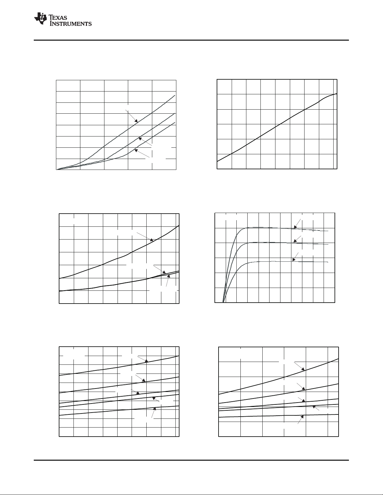
DETECTION BIAS CURRENT PoE CURRENT LIMIT
CONVERTER START TIME CONVERTER STARTUP SOURCE CURRENT
vs vs
VOLTAGE TEMPERATURE
Figure 3. Figure 4.
vs vs
TEMPERATURE V
VDD1
Figure 5. Figure 6.
CONTROLLER BIAS CURRENT CONTROLLER BIAS CURRENT
TEMPERATURE VOLTAGE
Copyright © 2008, Texas Instruments Incorporated Submit Documentation Feedback 9
Figure 7. Figure 8.
vs vs
Product Folder Link(s): TPS23753
Page 10

0
50
100
150
200
250
300
-40
-20
0
20
40
60
80
100 120
350
400
450
500
550
600
650
R =60.4k (250kHz)
FRS
W
R =30.1k (500kHz)
FRS
W
R =148.5k (100kHz)
FRS
W
R =301k (50kHz)
FRS
W
SwitchingFrequency-Hz
SwitchingFrequency-Hz
T -JunctionTemperature-°C
J
0
100
200
300
400
500
600
700
800
0 10 20 30 40 50
SwitchingFrequency-kHz
ProgrammedResistance(10 /R )-
6 -1
FRS
W
Ideal
Typical
76
76.5
77
77.5
78
78.5
79
-40
-20
0
20 40
60 80 100 120
MaximumDutyCycle-%
T -JunctionTemperature-°C
J
R =301k (50kHz)
FRS
W
R =148.5k (100kHz)
FRS
W
R =60.4k (250kHz)
FRS
W
R =30.1k (500kHz)
FRS
W
114
116
118
120
122
124
-40 -20 0 20 40 60 80 100 120
V -SlopeCompensation-mV
SLOPE
PP
T -JunctionTemperature-°C
J
TPS23753
SLVS853A – JUNE 2008 – REVISED JUNE 2008 ..............................................................................................................................................................
www.ti.com
TYPICAL CHARACTERISTICS (continued)
SWITCHING FREQUENCY SWITCHING FREQUENCY
MAXIMUM DUTY CYCLE CURRENT SLOPE COMPENSATION VOLTAGE
vs vs
TEMPERATURE PROGRAMMED RESISTANCE
Figure 9. Figure 10.
vs vs
TEMPERATURE TEMPERATURE
Figure 11. Figure 12.
10 Submit Documentation Feedback Copyright © 2008, Texas Instruments Incorporated
Product Folder Link(s): TPS23753
Page 11

30
35
40
45
50
-40 -20 0 20 40 60 80 100 120
I -SlopeCompensation- A
SL
OPE PP
m
T -JunctionTemperature-°C
J
45
55
65
75
85
95
105
115
-40 -20 0 20 40 60 80 100 120
235
240
245
250
255
260
265
270
T -JunctionTemperature-°C
J
BlankingPeriod(R <115k )-ns
BLNK
W
BlankingPeriod(R >115kW)-ns
BLN
K
R =RTN
BLNK
R =249k
BLNK
W
R =100k
BLNK
W
R =49.9k
BLNK
W
0
50
100
150
200
250
300
350
400
450
0 50 100 150 200 250 300 350 400
-18
-14
-10
-6
-2
2
6
10
14
18
BlankingPeriod-ns
R -k
BLNK
W
DifferencefromComputed-ns
TPS23753
www.ti.com
.............................................................................................................................................................. SLVS853A – JUNE 2008 – REVISED JUNE 2008
TYPICAL CHARACTERISTICS (continued)
CURRENT SLOPE COMPENSATION CURRENT BLANKING PERIOD
vs vs
TEMPERATURE TEMPERATURE
Figure 13. Figure 14.
BLANKING PERIOD
vs
R
BLNK
Copyright © 2008, Texas Instruments Incorporated Submit Documentation Feedback 11
Product Folder Link(s): TPS23753
Figure 15.
Page 12

Normal Operation
57
42
363020.514.510.12.7
Detection
Lower Limit
Detection
Upper Limit
C
l
a
s
s
i
f
i
c
a
t
i
o
n
L
o
w
e
r
L
i
m
i
t
Classification
Upper Limit
Must Turn Off by -
Volta ge Falling
Lower Limit -
Proper Operation
M
u
s
t
T
u
r
n
O
n
b
y
-
V
o
l
t
a
g
e
R
i
s
i
n
g
Maximum
Input
Voltage
Detect
Classify
Shutdown
PI Voltage (V)
0
3/06/08
TPS23753
SLVS853A – JUNE 2008 – REVISED JUNE 2008 ..............................................................................................................................................................
www.ti.com
APPLICATIONS
Classic PoE Overview
The following text is intended as an aid in understanding the operation of the TPS23753 but not as a substitute
for the actual IEEE 802.3-2005 or 802.3at standard. The pending IEEE 802.3at standard is an update to IEEE
802.3-2005 clause 33 (PoE), adding high-power options and enhanced classification. Generally speaking, a
device compliant to IEEE 802.3-2005 will be referred to as a Type 1 device, and devices with high power or
enhanced classification will be referred to as Type 2 devices. Standards change and should always be
referenced when making design decisions.
The IEEE 802.3-2005 (802.3at) standard defines a method of safely powering a PD (powered device) over a
cable, and then removing power if a PD is disconnected. The process proceeds through an idle state and three
operational states of detection, classification, and operation. The PSE leaves the cable unpowered (idle state)
while it periodically looks to see if something has been plugged in; this is referred to as detection. The low power
levels used during detection are unlikely to damage devices not designed for PoE. If a valid PD signature is
present, the PSE may inquire how much power the PD requires; this is referred to as classification. Type 2 PSEs
are required to do hardware classification. The PD may return the default 12.95W (often refered to as 13W)
current-encoded class, or one of four other choices. The PSE may then power the PD if it has adequate capacity.
Once started, the PD must present the maintain power signature (MPS) to assure the PSE that it is still present.
The PSE monitors its output for a valid MPS, and turns the port off if it loses the MPS. Loss of the MPS returns
the PSE to the idle state. Figure 16 shows the operational states as a function of PD input voltage.
Figure 16. IEEE 802.3-2005 (Type 1) Operational States
The PD input is typically an RJ-45 eight-lead connector which is referred to as the power interface (PI). PD input
requirements differ from PSE output requirements to account for voltage drops in the cable and operating
margin. The IEEE 802.3-2005 standard uses a cable resistance of 20 Ω to derive the voltage limits at the PD
based on the PSE output voltage requirements. Although the standard specifies an output power of 15.4 W at
the PSE, only 12.95 W is available at the PI due to the worst-case power loss in the cable. The PSE can apply
voltage either between the RX and TX pairs (pins 1 – 2 and 3 – 6 for 10baseT or 100baseT), or between the two
spare pairs (4 – 5 and 7 – 8). The PSE may only apply voltage to one set of pairs at a time. The PD uses input
diode bridges to accept power from any of the possible PSE configurations. The voltage drops associated with
the input bridges create a difference between the standard limits at the PI and the TPS23753 specifications.
The PSE is permitted to disconnect a PD if it draws more than its maximum class power over a one second
interval. A PSE compliant to IEEE 802.3-2005 is required to limit current to between 400 mA and 450 mA during
powered operation, and it must disconnect the PD if it draws this current for more than 75 ms. Class 0 and 3 PDs
may draw up to 400 mA peak currents for up to 50 ms. The PSE may set lower output current limits based on
the PD ’ s declared power requirements.
Threshold Voltages
The TPS23753 has a number of internal comparators with hysteresis for stable switching between the various
states as shown in Figure 16 . Figure 17 relates the parameters in the Electrical Characteristics section to the
PoE states. The mode labeled idle between classification and operation implies that the DEN, CLS, and RTN
pins are all high impedance.
12 Submit Documentation Feedback Copyright © 2008, Texas Instruments Incorporated
Product Folder Link(s): TPS23753
Page 13

V
UVLO_R
Detection
Classification
PD Powered
Idle
V
CL_ON
V
CL_HYS
1.4V
V
CU_OFF
V
CU_HYS
Note: Variable names refer to Electrical Characteristic
Table parameters
V
VDD-VSS
V
UVLO_H
Operational State
TPS23753
www.ti.com
.............................................................................................................................................................. SLVS853A – JUNE 2008 – REVISED JUNE 2008
Figure 17. Threshold Voltages
PoE Startup Sequence
The waveforms of Figure 18 demonstrate detection, classification, and startup from a PSE. The key waveforms
shown are V
VDD-VSS
four levels are shown in this example. Four levels guard against misdetection of a device when plugged in during
the detection sequence.
, V
RTN-VSS
, and IPI. IEEE 802.3-2005 requires a minimum of two detection levels, however
Figure 18. PoE Startup Sequence
Detection
The TPS23753 is in detection mode whenever V
input voltage rises above V
CL_ON
VDD-VSS
is below the lower classification threshold. When the
, the DEN pin goes to an open-drain condition to conserve power. While in
detection, RTN is high impedance, almost all the internal circuits are disabled, and the DEN pin is pulled to V
An R
of 24.9 k Ω (1%), presents the correct signature. It may be a small, low-power resistor since it only sees
DEN
a stress of about 5 mW. A valid PD detection signature is an incremental resistance between 23.75 k Ω and
26.25 k Ω at the PI.
Copyright © 2008, Texas Instruments Incorporated Submit Documentation Feedback 13
Product Folder Link(s): TPS23753
.
SS
Page 14

TPS23753
SLVS853A – JUNE 2008 – REVISED JUNE 2008 ..............................................................................................................................................................
www.ti.com
The detection resistance seen by the PSE at the PI is the result of the input bridge resistance in series with the
parallel combination of R
and the TPS23753 bias loading. The input diode bridge ’ s incremental resistance
DEN
may be hundreds of Ohms at the very low currents drawn when 2.7 V is applied to the PI. The input bridge
resistance is partially cancelled by the TPS23753's effective resistance during detection.
Hardware Classification
Hardware classification allows a PSE to determine a PD ’ s power requirements before starting and helps with
power management once power is applied. The maximum power entries in Table 2 determine the class the PD
must advertise. A Type 1 PD may not advertise Class 4. The PSE may disconnect a PD if it draws more than its
stated Class power. The standard permits the PD to draw limited current peaks, however the average power
requirement always applies.
Voltage between 14.5 V and 20.5 V is applied to the PD for up to 75 ms during hardware Classification. A fixed
output voltage is sourced by the CLS pin, causing a fixed current to be drawn from V
current drawn from the PSE during classification is the sum of bias and R
currents. PD current is measured
CLS
and decoded by the PSE to determine which of the five available classes is advertised (see Table 2 ). The
TPS23753 disables classification above V
CU_OFF
to avoid excessive power dissipation. CLS voltage is turned off
during PD thermal limit or when APD or DEN are active. The CLS output is inherently current limited, but should
not be shorted to V
for long periods of time.
SS
Table 2. Class Resistor Selection
POWER AT PD PI Class Current Requirement
CLASS RESISTOR ( Ω ) NOTES
0 0.44 12.95 0 4 1270
1 0.44 3.84 9 12 243
2 3.84 6.49 17 20 137
3 6.49 12.95 26 30 90.9
4 12.95 25.5 36 44 63.4
MINIMUM MAXIMUM
(W) (mA)
MAXIMUM (W) MINIMUM (mA)
through R
DD
802.3at only, not allowed for IEEE
802.3-2005 (type 1 devices)
CLS
. The total
Maintain Power Signature (MPS)
The MPS is an electrical signature presented by the PD to assure the PSE that it is still present after operating
voltage is applied. A valid MPS consists of a minimum dc current of 10 mA (at a duty cycle of at least 75 ms on
every 225 ms) and an ac impedance lower than 26.25 k Ω in parallel with 0.05 µ F. The ac impedance is usually
accomplished by the minimum C
requirement of 5 µ F. When APD or DEN are used to force the hotswap switch
IN
off, the dc MPS will not be met. A PSE that monitors the dc MPS will remove power from the PD when this
occurs. A PSE that monitors only the ac MPS may remove power from the PD.
TPS23753 Operation
Startup and Converter Operation
The internal PoE UVLO (Under Voltage Lock Out) circuit holds the hotswap switch off before the PSE provides
full voltage to the PD. This prevents the converter circuits from loading the PoE input during detection and
classification. The converter circuits will discharge C
will be a small voltage just after full voltage is applied to the PD, as seen in Figure 18 .
The PSE drives the PI voltage to the operating range once it has decided to power up the PD. When V
above the UVLO turn-on threshold (V
, ~35 V) with RTN high, the TPS23753 enables the hotswap
UVLO-R
MOSFET with a ~140 mA (inrush) current limit. Refer to the waveforms of Figure 19 for an example. Converter
switching is disabled while C
circuit is allowed to charge C
charges and V
IN
. Once the inrush current falls about 10% below the inrush current limit, the PD
VC
RTN
control switches to the operational level (~450 mA) and converter switching is permitted.
, C
IN
VC
falls from V
, and C
while the PD is unpowered. Thus V
VB
DD
to nearly V
, however the converter startup
SS
RTN-VDD
DD
rises
14 Submit Documentation Feedback Copyright © 2008, Texas Instruments Incorporated
Product Folder Link(s): TPS23753
Page 15

0
1
2
3
4
5
6
7
8
000.0E
10.0E-3 20.0E-3 30.0E-3 40.0E-3 50.0E-3 60.0E-3 70.0E-3 80.0E-3 90.0E-3 100.0E-
t-Time10-ms/DIV
-0.7
-0.6
-0.5
I
PI
VDD-RTN
VC-RTN
INRUSH
TurnON
V
OUT
50V/DIV
2V/DIV
10V/DIV
100mA/Div
Exaggeratedprimarysecondarysoftstarthandoff
TPS23753
www.ti.com
Converter switching is allowed if the PD is not in inrush and the V
Continuing the startup sequence shown in Figure 19 , V
M1 switching is inhibited by the status of the V
V
VC
exceeds UVLO
converter control-bias output rises to support V
startup occurs. Figure 19 shows a small droop in V
.............................................................................................................................................................. SLVS853A – JUNE 2008 – REVISED JUNE 2008
under-voltage lock out (UVLO) permits it.
C
regulator powers the internal converter circuits as
UVLO. The V
C
rises as the startup current source charges C
VC
B
rises. Startup current is turned off, converter switching is enabled, and a softstart cycle starts when V
(~9 V). V
1
falls as it powers both the internal circuits and the switching MOSFET gate. If the
VC
before it falls to UVLO
VC
while the output voltage rises smoothly and a successful
VC
– UVLO
1
(~5.5 V), a successful
1H
startup occurs.
and
VC
VC
Figure 19. Power Up and Start
If V
VDD-VSS
but the converter will still run. The converter will stop if V
~5.5 V), the hotswap is in inrush current limit, or 0% duty cycle is demanded by V
drops below the lower PoE UVLO (UVLO
– UVLO
R
, ~30.5 V), the hotswap MOSFET is turned off,
H
falls below the converter UVLO (UVLO
VC
(V
CTL
CTL
< V
the converter is in thermal shutdown.
PD Interface Features
The PD section has the following functions, with the first four covered above.
• Detection
• Classification
• V
• Orderly sequencing of C
to V
DD
UVLO
SS
charge and converter operation
IN
• Hotswap switch current limit
• Hotswap switch foldback
• Hotswap thermal protection
The internal hotswap MOSFET is protected against output faults with a current limit and deglitched foldback. The
PSE output cannot be relied on to protect the PD MOSFET against transient conditions, so the PD implements
its own protection. High stress conditions include converter output shorts, shorts from V
on the input line. An overload on the pass MOSFET engages the current limit, with V
V
rises above ~12 V for longer than ~400 µ s, the current limit reverts to the inrush limit, and turns the
RTN
converter off. The 400 µ s deglitch feature prevents momentary transients from causing a PD reset, provided that
to RTN, or transients
DD
RTN-VSS
rising as a result. If
recovery lies within the bounds of the hotswap and PSE protection. Figure 20 shows an example of recovery
from a 15 V PSE rising voltage step. The hotswap MOSFET goes into current limit, overshooting to a relatively
low current, recovers to 420 mA full current limit, and charges the input capacitor while the converter continues to
run. The MOSFET did not go into foldback because V
Copyright © 2008, Texas Instruments Incorporated Submit Documentation Feedback 15
Product Folder Link(s): TPS23753
RTN-VSS
was below 12 V after the 400 µ s deglitch.
, ~1.5 V), or
ZDC
– UVLO
1
,
H
Page 16

TPS23753
SLVS853A – JUNE 2008 – REVISED JUNE 2008 ..............................................................................................................................................................
www.ti.com
Figure 20. Response to PSE Step Voltage
The PD control has a thermal sensor that protects the internal hotswap MOSFET. Conditions like startup or
operation into a V
to RTN short cause high power dissipation in the MOSFET. An overtemperature shutdown
DD
(OTSD) turns off the hotswap MOSFET and class regulator, which are restarted after the device cools. The PD
state machine will always restart in inrush current limit when exiting from a PD overtemperature event.
Pulling DEN to V
during powered operation causes the internal hotswap MOSFET to turn off. This feature
SS
allows a PD with secondary-side adapter ORing to achieve adapter priority. Care must be taken with
synchronous converter topologies that can deliver power in both directions.
The hotswap switch will be forced off under the following conditions:
• V
• V
above V
APD
≤ V
DEN
PD_DIS
APDEN
when V
(~1.5 V)
VDD-VSS
is in the operational range
• PD over temperature
• V
VDD-VSS
< PoE UVLO (~30.5 V).
Converter Controller Features
The TPS23753 dc/dc controller implements a typical current-mode control as shown in Figure 2 . Features
include oscillator, overcurrent and PWM comparators, current-sense blanker, softstart, and gate driver. In
addition, an internal current-compensation ramp generator, frequency synchronization logic, thermal shutdown,
and startup current source with control are provided.
The TPS23753 is optimized for isolated converters, and does not provide an internal error amplifier. Instead, the
optocoupler feedback is directly fed to the CTL pin which serves as a current-demand control for the PWM and
converter. There is an offset of V
below V
will stop converter switching, while voltages above (V
ZDC
(~1.5 V) and 2:1 resistor divider between the CTL pin and the PWM. A V
ZDC
+ 2 × V
ZDC
) will not increase the
CSMAX
requested peak current in the switching MOSFET. Optocoupler biasing design is eased by this limited control
range.
The internal startup current source and control logic implement a bootstrap-type startup. The startup current
source charges C
operational power must come from a converter (bias winding) output. Loading on V
while C
charges, otherwise the converter may never start. The optocoupler will not load V
VC
is off. The converter will shut off when V
from V
VC
when the converter is disabled (either by the PD control or the V
DD1
falls below its lower UVLO. This can happen when power is removed
C
control), while
and V
C
C
must be minimal
B
when the converter
B
from the PD, or during a fault on a converter output rail. When one output is shorted, all the outputs fall in voltage
including the one that powers VC. The control circuit discharges V
until it hits the lower UVLO and turns off. A
C
restart will initiate as described in "Startup and Converter Operation" if the converter turns off and there is
sufficient V
voltage. This type of operation is sometimes referred to as “ hiccup mode, ” which provides robust
DD1
output short protection by providing time-average heating reduction of the output rectifier.
16 Submit Documentation Feedback Copyright © 2008, Texas Instruments Incorporated
Product Folder Link(s): TPS23753
CTL
Page 17

R
FBU
R
FBL
TLV431
R
OB
C
IZ
R
SS
C
SS
D
SS
FromRegulated
OutputVoltage
TPS23753
www.ti.com
Care in design of the transformer and V
Leading-edge voltage overshoot on the bias winding may cause V
tracking with output voltage. R
.............................................................................................................................................................. SLVS853A – JUNE 2008 – REVISED JUNE 2008
bias circuit is required to obtain hiccup overload protection.
C
(Figure 1 ) is often required slow the peak charging. Good transformer
VC
to peak-charge, preventing the expected
C
bias-to-output-winding coupling results in reduced overshoot and better voltage tracking.
The startup current source transitions to a resistance as (V
from 12 V adapters within tST(V
≥ 10.2, V~85 ms). The bootstrap source provides reliable startup from widely
DD1
- VC) falls below 7 V, but will start the converter
DD1
varying input voltages, and eliminates the continual power loss of external resistors. The startup current source
will not charge above the maximum recommended V
if the converter is disabled and there is sufficient V
VC
DD1
charge higher.
The peak current limit does not have duty cycle dependency unless R
is used as shown in Figure 22 to increase
S
slope compensation. This makes it easier to design the current limit to a fixed value.
The TPS23753 blanker timing is precise enough that the traditional R-C filters on CS can be eliminated. This
aviods current-sense waveform distortion, which tends to get worse at light output loads. While the internally set
blanking period is relatively precise, almost all converters will require their own blanking period. The TPS23753
provides the BLNK pin to allow this programming. There may be some situations or designers that prefer an R-C
approach. The TPS23753 provides a pull-down on CS during the GATE off time to improve sensing when an
R-C filter must be used. The CS input signal should be protected from nearby noisy signals like GATE drive and
the MOSFET drain.
Converters require a softstart on the voltage error amplifier to prevent output overshoot on startup. Figure 21
shows a common implementation of a secondary-side softstart that works with the typical TL431 error amplifier
shown in Figure 1 . This secondary-side error amplifier will not become active until there is sufficient voltage on
the secondary. The TPS23753 provides a primary-side softstart which persists long enough (~800 µ s) for
secondary side voltage-loop softstart to take over. The primary-side current-loop softstart controls the switching
MOSFET peak current by applying a slowly rising ramp voltage to a second PWM control input. Figure 19 shows
an exaggerated handoff between the primary and secondary-side softstart that is most easily seen in the I
waveform. The output voltage rises in a smooth monotonic fashion with no overshoot. This handoff can be
optimized by decreasing the secondary-side softstart period.
to
PI
Figure 21. Example of Softstart Circuit Added to Error Amplifier
The dc/dc controller has an OTSD that can be triggered by heat sources including the V
bootstrap current source, and bias currents. The controller OTSD turns off VB, the GATE driver, resets the
softstart generator, and forces the V
control into an under-voltage state.
C
regulator, GATE driver,
B
Special Switching MOSFET Considerations
Special care must be used in selecting the converter switching MOSFET. The TPS23753 converter section has
minimum V
output overload, or towards the end of a (failed) bootstrap startup. The MOSFET must be able to carry the
anticipated peak fault current at this gate voltage.
Copyright © 2008, Texas Instruments Incorporated Submit Documentation Feedback 17
C
operating voltage of ~5.5 V, which is reflected in the applied gate voltage. This will occur during an
Product Folder Link(s): TPS23753
Page 18

(
)
(
)
BLNK BLNK
R k t nsΩ =
TPS23753
SLVS853A – JUNE 2008 – REVISED JUNE 2008 ..............................................................................................................................................................
www.ti.com
Thermal Considerations
Sources of nearby local PCB heating should be considered during the thermal design. Typical calculations
assume that the TPS23753 is the only heat source contributing to the PCB temperature rise. It is possible for a
normally operating TPS23753 device to experience an OTSD event if it is excessively heated by a nearby
device.
Blanking – R
The TPS23753 BLNK feature permits programming of the blanking period with specified tolerance. Selection of
the blanking period is often empirical because it is affected by parasitics and thermal effects of every device
between the gate-driver and output capacitors.
There is a critical range of blanking period that is bounded on the short side by erratic operation, and on the long
side by potentially harmful switching-MOSFET and output rectifier currents during a short circuit. The minimum
blanking period prevents the current limit and PWM comparators from being falsely triggered by the inherent
current “ spike ” that occurs when the switching MOSFET turns on. The maximum blanking period is bounded by
the output rectifier's ability to withstand the currents experienced during a converter output short. A short on the
flyback transformer secondary will cause very large peak MOSFET currents that are worsened by longer
blanking periods. A long blanking time also increases the minimum load required before cycle skipping occurs in
a non-synchronous converter.
The TPS23753 provides a choice between internal fixed and programmable blanking periods. The blanking
period is specified as an increase in the minimum GATE on time over the inherent gate driver and comparator
delays. The default period (see the Electrical Characteristics table) is selected by connecting BLNK to RTN, and
the programmable period is set with a resistor from BLNK to RTN per the following equation.
BLNK
For example, a 100 ns period is programmed by a 100 k Ω resistor. For a brand-new design, it is recommended
that an initial blanking period of 125 ns be designed in. This period should be be tuned once the converter is
operational.
Current Slope Compensation
Current-mode control requires addition of a compensation ramp to the sensed inductor (flyback transformer)
current for stability at duty cycles near and over 50%. The TPS23753 has a maximum duty cycle limit of 80%,
permitting the design of wide input-range flyback converters with a lower voltage stress on the output rectifiers.
While the maximum duty cycle is 80%, converters may be designed that run at duty cycles well below 80% for a
narrower, 36 V to 57 V range. The TPS23753 provides a fixed internal compensation ramp that suffices for most
applications. R
works with ramp current (I
specification does not include the ~3 µ A fixed current that flows out of the CS pin.
Most current-mode control papers and application notes define the slope values in terms of V
voltage / switching period), however the electrical characteristics table specifies the slope peak (V
on an 80% duty cycle. Assuming that the desired slope, V
compute R
with voltages in mV, current in µ A, and the duty cycle is unitless (e.g. D
(see Figure 22 ) may be used if the internally provided slope compensation is not enough. It
S
per the following equation where V
S
= I
PK
, ~40 µ A) that flows out of the CS pin when the MOSFET is on. The I
SL-EX
PP
, D
SLOPE
SLOPE-D
, and I
MAX
(in mV/period), is based on the full period,
are from the electrical characteristics table
SL-EX
= 0.8).
MAX
/T
(peak ramp
S
) based
SLOPE
(5)
PK
18 Submit Documentation Feedback Copyright © 2008, Texas Instruments Incorporated
Product Folder Link(s): TPS23753
Page 19

_
_
( )
( )
( ) 1000
( )
SLOPE
SLOPE D
MAX
S
SL EX
V mV
V mV
D
R
I Aµ
−
Ω = ⋅
R
CS
GATE
CS
RTN
R
S
C
S
5/09/08
15000
( )
( )
FRS
SW
R k
f kHz
Ω =
RTN
FRS
R
FRS
47pF
Synchronization
Pulse
4/30/08
V
SYNC
T
SYNC
RTN
FRS
R
FRS
47pF
Synchronization
Pulse
4/30/08
V
SYNC
T
SYNC
1:1
1000pF
Example:
Pulse PA0184
TPS23753
www.ti.com
.............................................................................................................................................................. SLVS853A – JUNE 2008 – REVISED JUNE 2008
Figure 22. Additional Slope Compensation
C
may be required if the presence of R
S
appear at the C
pin. The TPS23753 has an internal pull-down on C
S
causes increased noise, due to adjacent signals like the gate drive, to
S
reduce cycle-to-cycle carry-over voltage on CS.
( ~500 Ω ) while the MOSFET is OFF to
S
(6)
FRS and Synchronization
The FRS pin programs the (free-running) oscillator frequency, and may also be used to synchronize the
TPS23753 converter to a higher frequency. The internal oscillator sets the maximum duty cycle at 80% and
controls the current-compensation ramp circuit. R
The TPS23753 may be synchronized to an external clock to eliminate beat frequencies from a sampled system,
or to place emission spectrum away from an RF input frequency. Synchronization may be accomplished by
applying a short pulse ( > 25 ns) of magnitude V
that the maximum free-running frequency is just below the desired synchronization frequency. The
synchronization pulse terminates the potential on-time period, and the off-time period doesn ’ t begin until the
pulse terminates. A short pulse is preferred to avoid reducing the potential on-time.
Figure 23 shows examples of non-isolated and transformer-coupled synchronization circuits The pulse at the
FRS pin should reach between 2.5 V and VB, with a minimum width of 22 ns (above 2.5 V) and rise/fall times
less than 10 ns. The FRS node should be protected from noise because it is high-impedance.
should be selected per the following equation.
FRS
to FRS as shown in Figure 23 . R
SYNC
should be chosen so
FRS
Adapter ORing
Many PoE-capable devices are designed to operate from either a wall adapter or PoE power. A local power
solution adds cost and complexity, but allows a product to be used if PoE is not available in a particular
Copyright © 2008, Texas Instruments Incorporated Submit Documentation Feedback 19
Figure 23. Synchronization
Product Folder Link(s): TPS23753
Page 20

TPS23753
58V
0.1uF
R
DEN
R
CLS
From Ethernet
Transformers
V
DD
V
SS
CLS
DEN
Low Voltage
Output
RTN
From Spare
Pairs or
Transformers
Power
Circuit
Adapter
Option 3
Adapter
Option 2
Adapter
Option 1
V
DD1
Optional for PoE Priority
5/8/08
TPS23753
SLVS853A – JUNE 2008 – REVISED JUNE 2008 ..............................................................................................................................................................
www.ti.com
installation. While most applications only require that the PD operate when both sources are present, the
TPS23753 supports forced operation from either of the power sources. Figure 24 illustrates three options for
diode ORing external power into a PD. Only one option would be used in any particular design. Option 1 applies
power to the TPS23753 PoE input, option 2 applies power between the TPS23753 PoE section and the power
circuit, and option 3 applies power to the output side of the converter. Each of these options has advantages and
disadvantages. A detailed discussion of the TPS23753 and ORing solutions is covered in application note
Advanced Adapter ORing Solutions using the TPS23753, literature number SLVA306 .
Figure 24. ORing Configurations
Preference of one power source presents a number of challenges. Combinations of adapter output voltage
(nominal and tolerance), power insertion point, and which source is prefered determine solution complexity.
Several factors which add to the complexity are the natural high-voltage selection of diode ORing (the simplest
method of combining sources), the current limit implicit in the PSE, and PD inrush and protection circuits
(necessary for operation and reliability). Creating simple and seamless solutions is difficult if not impossible for
many of the combinations. However the TPS23753 offers several built-in features that simplify some
combinations.
Several examples will demonstrate the limitations inherent in ORing solutions. Diode ORing a 48 V adapter with
PoE (option 1) presents the problem that either source might be higher. A blocking switch would be required to
assure which source was active. A second example is combining a 12 V adapter with PoE using option 2. The
converter will draw approximately four times the current at 12 V from the adapter than it does from PoE at 48 V.
Transition from adapter power to PoE may demand more current than can be supplied by the PSE. The
converter must be turned off while C
capacitance charges, with a subsequent converter restart at the higher
IN
voltage and lower input current. A third example is use of a 12 V adapter with ORing option 1. The PD hotswap
would have to handle four times the current, and have 1/16 the resistance (be 16 times larger) to dissipate equal
power. A fourth example is that MPS is lost when running from the adapter, causing the PSE to remove power
from the PD. If ac power is then lost, the PD will stop operating until the PSE detects and powers the PD.
The most popular preferential ORing scheme is option 2 with adapter priority. The hotswap MOSFET is disabled
when the adapter is used to pull APD high, blocking the PoE source from powering the output. This solution
works well with a wide range of adapter voltages, is simple, and requires few external parts. When the ac power
fails, or the adapter is removed, the hotswap switch is enabled. In the simplest implementation, the PD will
momentarily loose power until the PSE completes its startup cycle.
The DEN pin can be used to disable the PoE input when ORing with option 3. This is an adapter priority
implementation. Pulling DEN low, while creating an invalid detection signature, disables the hotswap MOSFET
and prevents the PD from redetecting. This would typically be accomplished with an optocoupler that is driven
from the secondary side of the converter.
20 Submit Documentation Feedback Copyright © 2008, Texas Instruments Incorporated
Product Folder Link(s): TPS23753
Page 21

+
-
49.9kΩ
10kΩ4.99kΩ
6.04kΩ
10kΩ
0.01µF
301kΩ
1uF
V
B
To
FRS
RTN
TL331IDBV
TPS23753
www.ti.com
.............................................................................................................................................................. SLVS853A – JUNE 2008 – REVISED JUNE 2008
The least popular technique is PoE priority. It is implemented by placing a diode between the PD supply voltage,
V
, and the dc/dc controller bias voltage, V
DD
. The diode prevents reverse biasing of the PoE input diode
DD1
bridges when option 2 adapter ORing is used. The PSE may then detect, classify, and provide power to the PD
while a live adapter is connected. As long as the PoE voltage is greater than the adapter voltage, the PSE will
power the load. The APD function is not used in this technique.
The IEEE standards require that the Ethernet cable be isolated from ground and all other system potentials. The
adapter must meet a minimum 1500 Vac dielectric withstand test between the output and all other connections
for options 1 and 2. The adapter only needs this isolation for option 3 if it is not provided by the converter.
Adapter ORing diodes are shown for all the options to protect against a reverse voltage adapter, a short on the
adapter input pins, and damage to a low-voltage adapter. ORing is sometimes accomplished with a MOSFET in
option 3.
Protection
A TVS across the rectified PoE voltage per Figure 1 must be used. An SMAJ58A, or a part with equal to or better
performance, is recommended for general indoor applications. If an adapter is connected from V
DD1
to RTN, as
in ORing option 2 above, voltage transients caused by the input cable inductance ringing with the internal PD
capacitance can occur. Adequate capacitive filtering or a TVS must limit this voltage to be within the absolute
maximum ratings
Outdoor applications require more extensive protection to lightning standards.
Frequency Dithering for Conducted Emissions Control
The international standard CISPR 22 (and adopted versions) is often used as a requirement for conducted
emissions. Ethernet cables are covered as a telecommunication port under section 5.2 for conducted emissions.
Meeting EMI requirements is often a challenge, with the lower limits of Class B being especially hard. Circuit
board layout, filtering, and snubbing various nodes in the power circuit are the first layer of control techniques. A
more detailed discussion of EMI control is presented in Practical Guidelines to Designing an EMI Compliant PoE
Powered Device With Isolated Flyback, TI literature number SLUA469 . Additionally, IEEE802.3-2005 section 33.4
has requirements for noise injected onto the Ethernet cable based on compatibility with data transmission.
Occasionally, a technique referred to as frequency dithering is utilized to provide additional EMI measurement
reduction. The switching frequency is modulated to spread the narrowband individual harmonics across a wider
bandwidth, thus lowering peak measurements. The circuit of Figure 25 modulates the switching frequency by
feeding a small ac signal into the FRS pin. These values may be adapted to suit individual needs.
Figure 25. Frequency Dithering
Design Procedure
A detailed design procedure for PDs using the TPS23753 is covered in Designing with the TPS23753 Powered
Device and Power Supply Controller , literature number SLVA305 .
Copyright © 2008, Texas Instruments Incorporated Submit Documentation Feedback 21
Product Folder Link(s): TPS23753
Page 22

TPS23753
SLVS853A – JUNE 2008 – REVISED JUNE 2008 ..............................................................................................................................................................
www.ti.com
References
IEEE Standard for Information Technology … Part 3: Carrier sense multiple access with collision detection
(CSMA/CD) access method and physical layer specifications, IEEE Computer Society, IEEE 802.3™-2005
(Clause 33)
Information technology equipment – Radio disturbance characteristics – Limits and methods of measurement,
International Electrotechnical Commission, CISPR 22 Edition 5.2, 2006-03
Designing with the TPS23753 Powered Device and Power Supply Controller, Eric Wright, TI, SLVA305
Advanced Adapter ORing Solutions using the TPS23753, Eric Wright, TI, SLVA306
Practical Guidelines to Designing an EMI-Compliant PoE Powered Device With Isolated Flyback, Donald V.
Comiskey, TI, SLUA469
22 Submit Documentation Feedback Copyright © 2008, Texas Instruments Incorporated
Product Folder Link(s): TPS23753
Page 23

PACKAGE OPTION ADDENDUM
www.ti.com
11-Jul-2008
PACKAGING INFORMATION
Orderable Device Status
(1)
Package
Type
Package
Drawing
Pins Package
Qty
Eco Plan
TPS23753PW ACTIVE TSSOP PW 14 90 Green (RoHS &
no Sb/Br)
TPS23753PWG4 ACTIVE TSSOP PW 14 90 Green (RoHS &
no Sb/Br)
TPS23753PWR ACTIVE TSSOP PW 14 2000 Green (RoHS &
no Sb/Br)
TPS23753PWRG4 ACTIVE TSSOP PW 14 2000 Green (RoHS &
no Sb/Br)
(1)
The marketing status values are defined as follows:
ACTIVE: Product device recommended for new designs.
LIFEBUY: TI has announced that the device will be discontinued, and a lifetime-buy period is in effect.
NRND: Not recommended for new designs. Device is in production to support existing customers, but TI does not recommend using this part in
a new design.
PREVIEW: Device has been announced but is not in production. Samples may or may not be available.
OBSOLETE: TI has discontinued the production of the device.
(2)
Eco Plan - The planned eco-friendly classification: Pb-Free (RoHS), Pb-Free (RoHS Exempt), or Green (RoHS & no Sb/Br) - please check
http://www.ti.com/productcontent for the latest availability information and additional product content details.
TBD: The Pb-Free/Green conversion plan has not been defined.
Pb-Free (RoHS): TI's terms "Lead-Free" or "Pb-Free" mean semiconductor products that are compatible with the current RoHS requirements
for all 6 substances, including the requirement that lead not exceed 0.1% by weight in homogeneous materials. Where designed to be soldered
at high temperatures, TI Pb-Free products are suitable for use in specified lead-free processes.
Pb-Free (RoHS Exempt): This component has a RoHS exemption for either 1) lead-based flip-chip solder bumps used between the die and
package, or 2) lead-based die adhesive used between the die and leadframe. The component is otherwise considered Pb-Free (RoHS
compatible) as defined above.
Green (RoHS & no Sb/Br): TI defines "Green" to mean Pb-Free (RoHS compatible), and free of Bromine (Br) and Antimony (Sb) based flame
retardants (Br or Sb do not exceed 0.1% by weight in homogeneous material)
(2)
Lead/Ball Finish MSL Peak Temp
CU NIPDAU Level-1-260C-UNLIM
CU NIPDAU Level-1-260C-UNLIM
CU NIPDAU Level-1-260C-UNLIM
CU NIPDAU Level-1-260C-UNLIM
(3)
(3)
MSL, Peak Temp. -- The Moisture Sensitivity Level rating according to the JEDEC industry standard classifications, and peak solder
temperature.
Important Information and Disclaimer:The information provided on this page represents TI's knowledge and belief as of the date that it is
provided. TI bases its knowledge and belief on information provided by third parties, and makes no representation or warranty as to the
accuracy of such information. Efforts are underway to better integrate information from third parties. TI has taken and continues to take
reasonable steps to provide representative and accurate information but may not have conducted destructive testing or chemical analysis on
incoming materials and chemicals. TI and TI suppliers consider certain information to be proprietary, and thus CAS numbers and other limited
information may not be available for release.
In no event shall TI's liability arising out of such information exceed the total purchase price of the TI part(s) at issue in this document sold by TI
to Customer on an annual basis.
Addendum-Page 1
Page 24

PACKAGE MATERIALS INFORMATION
www.ti.com
TAPE AND REEL INFORMATION
3-Jul-2008
*All dimensions are nominal
Device Package
TPS23753PWR TSSOP PW 14 2000 330.0 12.4 7.0 5.6 1.6 8.0 12.0 Q1
Type
Package
Drawing
Pins SPQ Reel
Diameter
(mm)
Reel
Width
W1 (mm)
A0 (mm) B0 (mm) K0 (mm) P1
(mm)W(mm)
Pin1
Quadrant
Pack Materials-Page 1
Page 25

PACKAGE MATERIALS INFORMATION
www.ti.com
3-Jul-2008
*All dimensions are nominal
Device Package Type Package Drawing Pins SPQ Length (mm) Width (mm) Height (mm)
TPS23753PWR TSSOP PW 14 2000 346.0 346.0 29.0
Pack Materials-Page 2
Page 26

MECHANICAL DATA
MTSS001C – JANUARY 1995 – REVISED FEBRUARY 1999
PW (R-PDSO-G**) PLASTIC SMALL-OUTLINE PACKAGE
14 PINS SHOWN
0,65
1,20 MAX
14
0,30
0,19
8
4,50
4,30
PINS **
7
Seating Plane
0,15
0,05
8
1
A
DIM
6,60
6,20
14
0,10
0,10
M
0,15 NOM
Gage Plane
0,25
0°–8°
2016
24
28
0,75
0,50
A MAX
A MIN
NOTES: A. All linear dimensions are in millimeters.
B. This drawing is subject to change without notice.
C. Body dimensions do not include mold flash or protrusion not to exceed 0,15.
D. Falls within JEDEC MO-153
3,10
2,90
5,10
4,90
5,10
4,90
6,60
6,40
7,90
7,70
9,80
9,60
4040064/F 01/97
POST OFFICE BOX 655303 • DALLAS, TEXAS 75265
Page 27

IMPORTANT NOTICE
Texas Instruments Incorporated and its subsidiaries (TI) reserve the right to make corrections, modifications, enhancements, improvements,
and other changes to its products and services at any time and to discontinue any product or service without notice. Customers should
obtain the latest relevant information before placing orders and should verify that such information is current and complete. All products are
sold subject to TI’s terms and conditions of sale supplied at the time of order acknowledgment.
TI warrants performance of its hardware products to the specifications applicable at the time of sale in accordance with TI’s standard
warranty. Testing and other quality control techniques are used to the extent TI deems necessary to support this warranty. Except where
mandated by government requirements, testing of all parameters of each product is not necessarily performed.
TI assumes no liability for applications assistance or customer product design. Customers are responsible for their products and
applications using TI components. To minimize the risks associated with customer products and applications, customers should provide
adequate design and operating safeguards.
TI does not warrant or represent that any license, either express or implied, is granted under any TI patent right, copyright, mask work right,
or other TI intellectual property right relating to any combination, machine, or process in which TI products or services are used. Information
published by TI regarding third-party products or services does not constitute a license from TI to use such products or services or a
warranty or endorsement thereof. Use of such information may require a license from a third party under the patents or other intellectual
property of the third party, or a license from TI under the patents or other intellectual property of TI.
Reproduction of TI information in TI data books or data sheets is permissible only if reproduction is without alteration and is accompanied
by all associated warranties, conditions, limitations, and notices. Reproduction of this information with alteration is an unfair and deceptive
business practice. TI is not responsible or liable for such altered documentation. Information of third parties may be subject to additional
restrictions.
Resale of TI products or services with statements different from or beyond the parameters stated by TI for that product or service voids all
express and any implied warranties for the associated TI product or service and is an unfair and deceptive business practice. TI is not
responsible or liable for any such statements.
TI products are not authorized for use in safety-critical applications (such as life support) where a failure of the TI product would reasonably
be expected to cause severe personal injury or death, unless officers of the parties have executed an agreement specifically governing
such use. Buyers represent that they have all necessary expertise in the safety and regulatory ramifications of their applications, and
acknowledge and agree that they are solely responsible for all legal, regulatory and safety-related requirements concerning their products
and any use of TI products in such safety-critical applications, notwithstanding any applications-related information or support that may be
provided by TI. Further, Buyers must fully indemnify TI and its representatives against any damages arising out of the use of TI products in
such safety-critical applications.
TI products are neither designed nor intended for use in military/aerospace applications or environments unless the TI products are
specifically designated by TI as military-grade or "enhanced plastic." Only products designated by TI as military-grade meet military
specifications. Buyers acknowledge and agree that any such use of TI products which TI has not designated as military-grade is solely at
the Buyer's risk, and that they are solely responsible for compliance with all legal and regulatory requirements in connection with such use.
TI products are neither designed nor intended for use in automotive applications or environments unless the specific TI products are
designated by TI as compliant with ISO/TS 16949 requirements. Buyers acknowledge and agree that, if they use any non-designated
products in automotive applications, TI will not be responsible for any failure to meet such requirements.
Following are URLs where you can obtain information on other Texas Instruments products and application solutions:
Products Applications
Amplifiers amplifier.ti.com Audio www.ti.com/audio
Data Converters dataconverter.ti.com Automotive www.ti.com/automotive
DSP dsp.ti.com Broadband www.ti.com/broadband
Clocks and Timers www.ti.com/clocks Digital Control www.ti.com/digitalcontrol
Interface interface.ti.com Medical www.ti.com/medical
Logic logic.ti.com Military www.ti.com/military
Power Mgmt power.ti.com Optical Networking www.ti.com/opticalnetwork
Microcontrollers microcontroller.ti.com Security www.ti.com/security
RFID www.ti-rfid.com Telephony www.ti.com/telephony
RF/IF and ZigBee® Solutions www.ti.com/lprf Video & Imaging www.ti.com/video
Mailing Address: Texas Instruments, Post Office Box 655303, Dallas, Texas 75265
Copyright © 2008, Texas Instruments Incorporated
Wireless www.ti.com/wireless
 Loading...