

Page 1

User's Guide
SLVUB75A–August 2017–Revised September 2017
TPS2372-4EVM-006 Evaluation Module
This user’s guide describes the TPS2372-4 evaluation module (TPS2372-4EVM-006). The TPS23724EVM-006 contains evaluation and reference circuitry for the TPS2372-4. The TPS2372-4 device is an
IEEE 802.3bt compliant, powered-device (PD) controller optimized for high power, power-over-Ethernet
(PoE) PD applications such as LED lighting and high-power module applications.
Contents
1 Introduction ................................................................................................................... 2
1.1 Features.............................................................................................................. 2
1.2 Applications.......................................................................................................... 2
2 Electrical Specifications..................................................................................................... 2
3 Description.................................................................................................................... 2
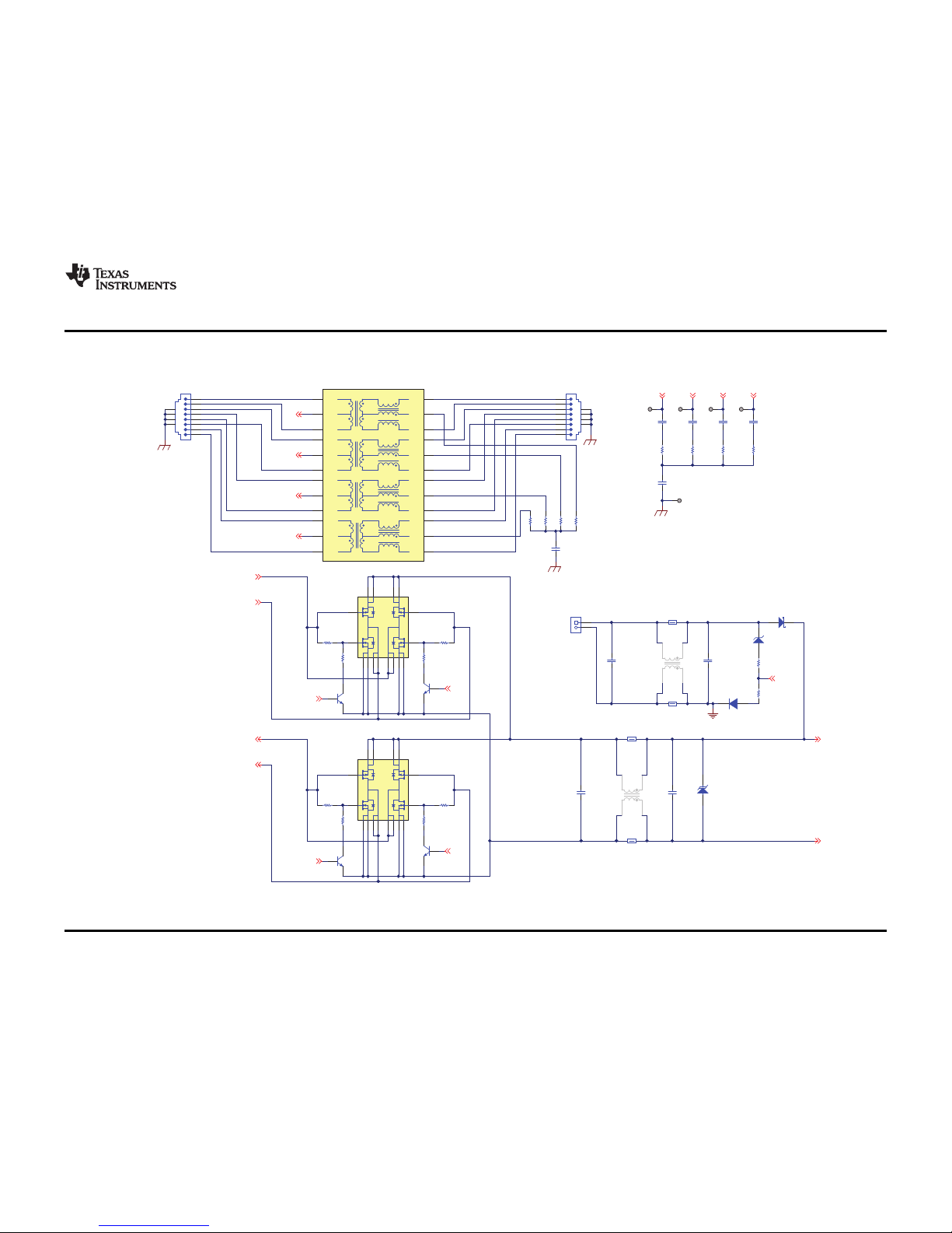
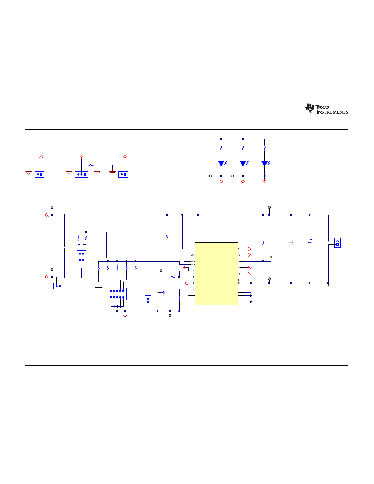
4 Schematic..................................................................................................................... 3
5 General Configuration and Description ................................................................................... 5
5.1 Physical Access..................................................................................................... 5
6 TPS2372-4EVM-006 Performance Data ................................................................................. 6
7 EVM Assembly Drawing and Layout Guidelines ........................................................................ 8
7.1 PCB Drawings....................................................................................................... 8
7.2 Layout Guidelines ................................................................................................. 11
7.3 EMI Containment.................................................................................................. 12
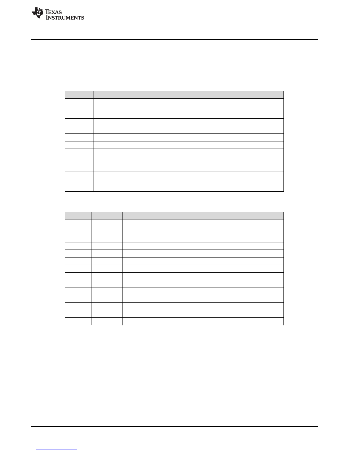
8 Bill of Material............................................................................................................... 13
List of Figures
1 TPS2372-4EVM-006 Front End Interface Schematic................................................................... 3
2 TPS2372-4EVM-006 PD Controller Schematic ......................................................................... 4
3 Startup using.bt PSE and Autoclass Enabled ........................................................................... 6
4 PD Startup With Delay...................................................................................................... 6
5 Current-Limit Protection Performance .................................................................................... 6
6 Auto MPS ..................................................................................................................... 7
7 Top Side Component Placement.......................................................................................... 8
8 Top Side Routing ............................................................................................................ 8
9 Layer 2 Routing .............................................................................................................. 9
10 Layer 3 Routing .............................................................................................................. 9
11 Bottom Side Routing....................................................................................................... 10
12 Bottom Component Placement........................................................................................... 10
List of Tables
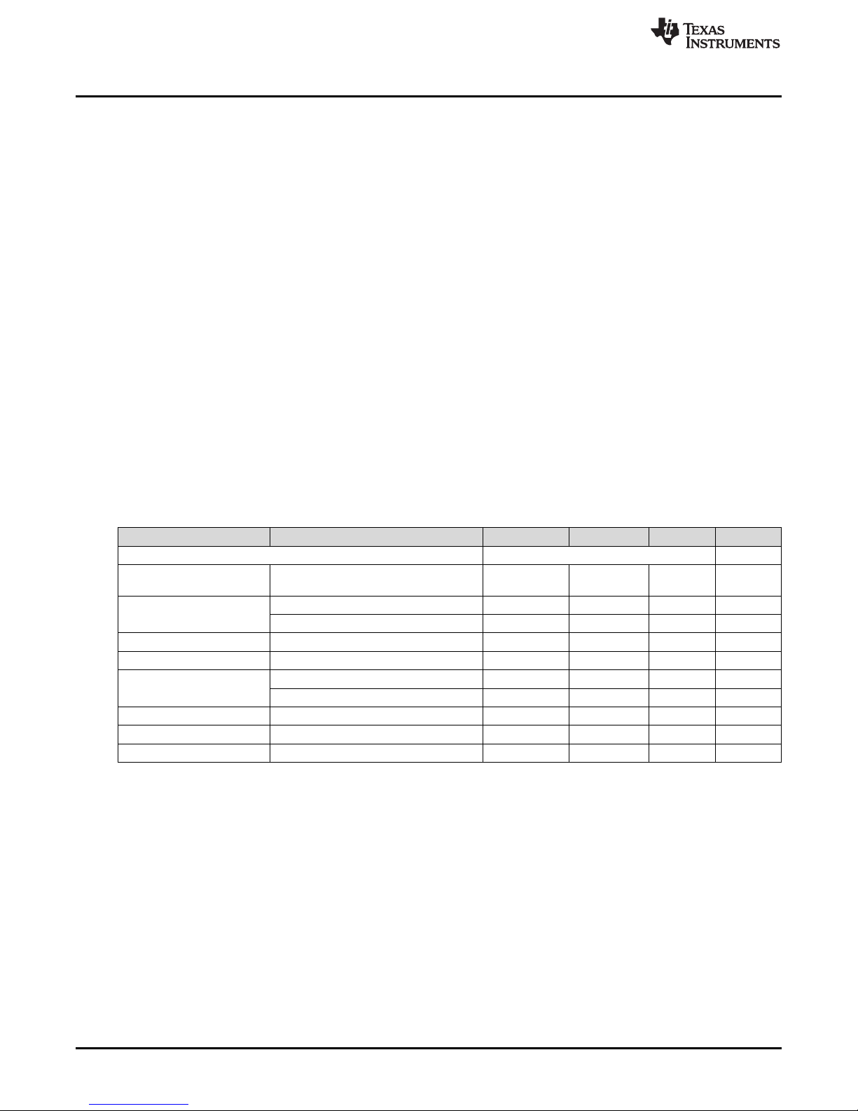
1 TPS2372-4EVM-006 Electrical and Performance Specifications at 25°C............................................ 2
2 Connector Functionality..................................................................................................... 5
3 Test Points.................................................................................................................... 5
4 TPS2372-4EVM-006 BOM ............................................................................................... 13
SLVUB75A–August 2017–Revised September 2017
Submit Documentation Feedback
Copyright © 2017, Texas Instruments Incorporated
TPS2372-4EVM-006 Evaluation Module
1
Page 2
Introduction
1 Introduction
The TPS2372-4EVM-006 allows reference circuitry evaluation of the TPS2372-4. It contains input and
output power connectors and an array of on-board test points for circuit evaluation.
1.1 Features
The TPS2372-4EVM-006 features include:
• High-power PoE
• Selectable classification
• Adjustable auto MPS
• Gigabit Ethernet pass-through interface
1.2 Applications
The TPS2372-4EVM-006 can be used in the following applications:
• Power-over-Ethernet (PoE) lighting
• Internet of Things (IoT)
• PoE modules
2 Electrical Specifications
Table 1 lists the EVM electrical specifications.
www.ti.com
Table 1. TPS2372-4EVM-006 Electrical and Performance Specifications at 25°C
Parameter Test Conditions Min Typ Max Unit
Power Interface
Input voltage Applied to the power pins of connectors
Input UVLO, PoE input J1
Detection voltage At device terminals 3 10 V
Classification voltage At device terminals 10 23 V
Classification current
Inrush current-limit 275 395 mA
Operating current-limit 1.9 2.5 A
Adatper voltage 42.5 57 V
3 Description
The TPS2372-4EVM-006 enables full evaluation of the TPS2372-4 device, see the schematic in Figure 1.
Ethernet power is applied from J1 and is dropped to the FET bridge rectifier. At the output of the FET
bridge is the EMI/EMC filter and transient protection for the TPS2372-4.
Input power can also be applied at J3 from a DC source when power at J1 is not present.
The TPS2372-4 (U1) PD controller is shown in Figure 1. R23 provides the detection signature. To the right
of U2 is the switched side of the PD controller. The TPS2372-4 RTN pin provides inrush limited turn on
and the charge of the bulk capacitor C11.
J2 or J4
0 57 V
Rising input voltage 36 V
Falling input voltage 30 V
RclassA = 63.4 Ω 38 42 mA
RclassB = 90.9 Ω 26.5 29.3 mA
2
TPS2372-4EVM-006 Evaluation Module
SLVUB75A–August 2017–Revised September 2017
Copyright © 2017, Texas Instruments Incorporated
Submit Documentation Feedback
Page 3
1000pF
C9
1000pF
C10
VDD
VSS1
2
1
58V
D3
1000pF
C7
1000pF
C8
42.5-57VDC
GND
D1
300 ohm
L1
300 ohm
L3
300 ohm
L4
300 ohm
L6
1
2
J3
RTN
75.0
R1
75.0R275.0R375.0
R4
ETHERNET POWER
42.5-57VDC
71W MAX
DATA PORT
PR12 PR36 PR45 PR78
EARTH
TCT1
1
TD1+
2
TD1-
3
TCT2
4
TD2+
5
TD2-
6
TCT3
7
TD3+
8
TD3-
9
TCT4
10
TD4+
11
TD4-
12
MX4-
13
MX4+
14
MCT4
15
MX3-
16
MX3+
17
MCT3
18
MX2-
19
MX2+
20
MCT2
21
MX1-
22
MX1+
23
MCT4
24
T1
7490220122
PR12
PR36
PR45
PR78
TP1 TP2 TP3 TP4
PAIR12 PAIR36 PAIR45 PAIR78
EARTH
TP5
1000pF
C5
2
3
4
1
5
6
7
8
9
10
11
12
J2
EARTH
EARTH
75.0
R8
75.0R575.0
R7
75.0
R6
EARTH
1
2
3
4
L5
DNP
1
2
3
4
L2
DNP
131415
16
1
2
3
4
5
678
9
10
11
12
Q1
PR12
PR36
20.0k
R14
20.0k
R13
6.8k
R9
6.8k
R10
8.2k
R11
8.2k
R12
3
1
2
Q2
3
1
2
Q3
12V
D2
131415
16
1
2
3
4
5
678
9
10
11
12
Q4
6.8k
R15
6.8k
R16
8.2k
R17
8.2k
R18
3
1
2
Q5
3
1
2
Q6
PR45
PR78
BR_OFF
BR_OFF
BR_OFF
BR_OFF
BR_OFF
0.01µFC10.01µFC20.01µFC30.01µF
C4
1000pF
C6
D7
2
3
4
1
5
6
7
8
9
10
11
12
J1
Copyright © 2017, Texas Instruments Incorporated
www.ti.com
Schematic
3
SLVUB75A–August 2017–Revised September 2017
Submit Documentation Feedback
Copyright © 2017, Texas Instruments Incorporated
TPS2372-4EVM-006 Evaluation Module
4 Schematic
Figure 1 and Figure 2 illustrate the TPS2372-4EVM-006 schematics.
Figure 1. TPS2372-4EVM-006 Front End Interface Schematic
Page 4
VDD
VSS1
63.4
R24
AUTCLS
Yellow
D4
TPH
TPL
BT
49.9k
R26
MPS_DUTY
MPS_DUTY
AUTCLS
VSS
VSS
123
J4
TSM-103-01-L-SV-P-TR
VSS
53.6k
R22
VSS
49.9k
R34
IRSHDL_EN
IRSHDL_EN
RTN
Yellow
D5
Yellow
D6
TPH TPL BT
47µF
C12
DNP
90.9
R27
21.0k
R19
21.0k
R20
21.0k
R21
2k
R33
1.0k
R32
TP9
TP14
VDD
VSS1
Port Current
Class 8
Class 7
Class 6
Class 5
TP12
AMPS_CTL
AMPS_Connect
TP11
PG
TP13
RTN
TPH TPL BT
63.4
R31
123456789
10
J9
Class 4
4-Pair
90.9
R25
Class 4
Class 3
TP10
VDD
TP15
VSS
0.1µF
C13
J10
J11
J5 J6
TP6 TP7 TP8
123
4
J8
VDD
1
DEN
2
CLS1
3
VSS
4
VSS
5
CLS2
6
REF
7
AMPS_CTL
8
MPS_DUTY
9
AUTCLS
10
RTN
11
RTN
12
PG
13
NC
14
NC
15
IRSHDL_EN
16
TPL
17
TPH
18
BT
19
NC
20
PAD
21
U1
TPS2372-4RGWR
24.9k
R23
1.21k
R30
249
R29
140
R28
1
2
J7
VDD
RTN
RTN
100µF
C11
Copyright © 2017, Texas Instruments Incorporated
Schematic
www.ti.com
4
SLVUB75A–August 2017–Revised September 2017
Submit Documentation Feedback
Copyright © 2017, Texas Instruments Incorporated
TPS2372-4EVM-006 Evaluation Module
Figure 2. TPS2372-4EVM-006 PD Controller Schematic
Page 5
www.ti.com
5 General Configuration and Description
5.1 Physical Access
Table 2 lists the EVM connector functionality and Table 3 describes the test point availability.
Table 2. Connector Functionality
Connector Label Description
J1 ETHERNET
POWER
J2 DATA Ethernet data pass-through. Connect to downstream Ethernet device.
J7 Output Output connector to load
J3 AdapterInput DC Adapter input. Connect to DC power supply.
J4 MPS_Duty Automatic MPS duty cycle selection
J5 /AUTCLS Jump to enable autoclass
J6 IRSHDL_EN Jump to disable inrush delay
J8 CLSA Jump to select Class current level
J9 CLSB Jump to select Class current level
J10 Port Current Jump connect PD front end and PD controller circuits
J11 AMPS_Conn
ect
PoE input. Connect to PSE power and data source.
Jump to add auto MPS current
General Configuration and Description
Table 3. Test Points
Test Point Label Description
TP1 PAIR 12 Data pair from pins 1 and 2 of J1
TP2 PAIR 36 Data pair from pins 3 and 6 of J1
TP3 PAIR 45 Spare pair from pins 4 and 5 of J1
TP4 PAIR 78 Spare pair from pins 7 and 8 of J1
TP5 EARTH Connect to earth ground, when available
TP6 TPH TPH output of the TPS2372-4
TP7 TPL TPL output of the TPS2372-4
TP8 BT BT output of the TPS2372-4
TP9, TP10 VDD Input voltage of PD system
TP11 PG Power Good output fo the TPS2372-4
TP12 AMPS_CTL AMPS_CTL output voltage
TP13 RTN Load side return voltage
TP14 VSS1 EMI filter return side voltage
TP15 VSS PD side return voltage
SLVUB75A–August 2017–Revised September 2017
Submit Documentation Feedback
Copyright © 2017, Texas Instruments Incorporated
TPS2372-4EVM-006 Evaluation Module
5
Page 6
PG
VDD-VSS
IIH
RTH-VSS
PG
VDD-VSS
RTH-VSS
IIN
RTN-VSS
VDD-VSS
IIN
TPS2372-4EVM-006 Performance Data
6 TPS2372-4EVM-006 Performance Data
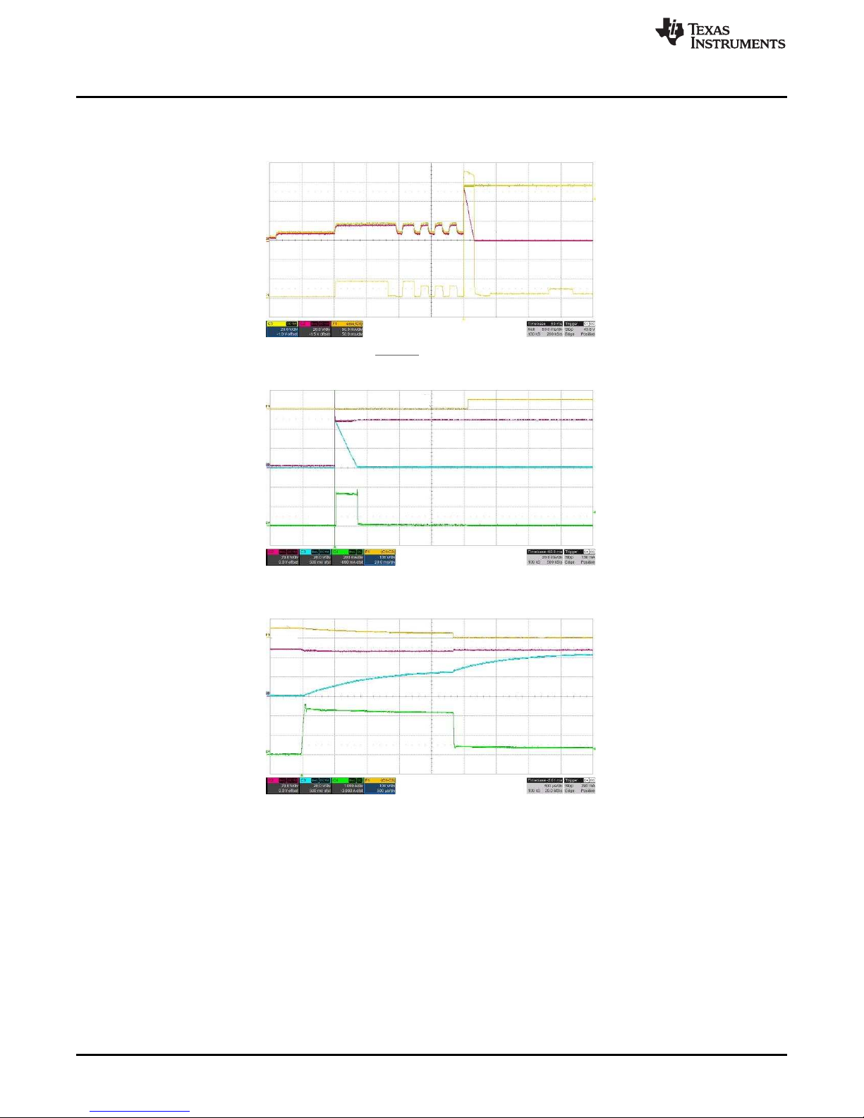
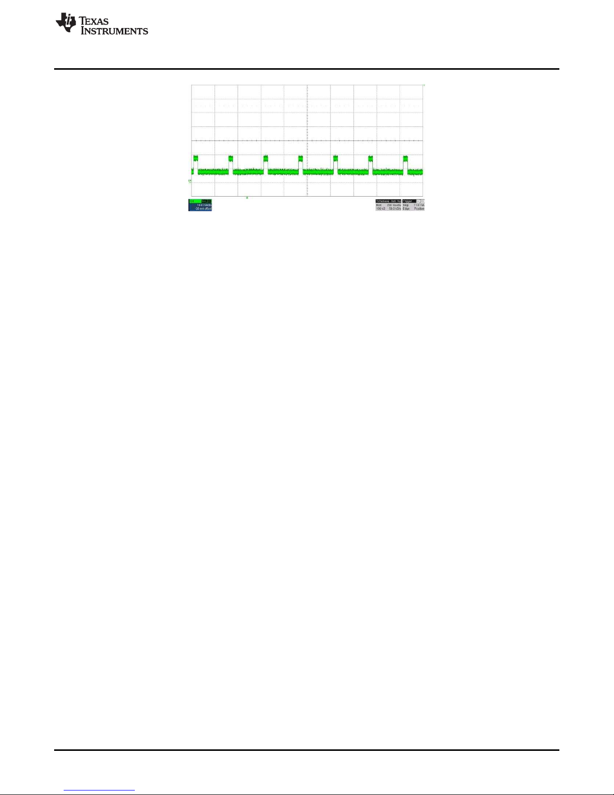
Figure 3 through Figure 6 illustrate EVM performance waveforms.
Figure 3. Startup !~using!~With!~.bt PSE!~ and Autoclass Enabled
www.ti.com
Figure 4. PD Startup With Delay
Figure 5. Current-Limit Protection Performance
6
TPS2372-4EVM-006 Evaluation Module
SLVUB75A–August 2017–Revised September 2017
Copyright © 2017, Texas Instruments Incorporated
Submit Documentation Feedback
Page 7
IIN
www.ti.com
TPS2372-4EVM-006 Performance Data
Figure 6. Auto MPS
SLVUB75A–August 2017–Revised September 2017
Submit Documentation Feedback
Copyright © 2017, Texas Instruments Incorporated
TPS2372-4EVM-006 Evaluation Module
7
Page 8

EVM Assembly Drawing and Layout Guidelines
7 EVM Assembly Drawing and Layout Guidelines
7.1 PCB Drawings
Figure 7 through Figure 12 show component placement and layout of the TPS237xEVM-006.
www.ti.com
Figure 7. Top Side Component Placement
Figure 8. Top Side Routing
8
TPS2372-4EVM-006 Evaluation Module
SLVUB75A–August 2017–Revised September 2017
Copyright © 2017, Texas Instruments Incorporated
Submit Documentation Feedback
Page 9

www.ti.com
EVM Assembly Drawing and Layout Guidelines
Figure 9. Layer 2 Routing
SLVUB75A–August 2017–Revised September 2017
Submit Documentation Feedback
Figure 10. Layer 3 Routing
Copyright © 2017, Texas Instruments Incorporated
TPS2372-4EVM-006 Evaluation Module
9
Page 10

EVM Assembly Drawing and Layout Guidelines
Figure 11. Bottom Side Routing
www.ti.com
10
TPS2372-4EVM-006 Evaluation Module
Figure 12. Bottom Component Placement
SLVUB75A–August 2017–Revised September 2017
Copyright © 2017, Texas Instruments Incorporated
Submit Documentation Feedback
Page 11

www.ti.com
7.2 Layout Guidelines
The layout of the PoE front end should follow power and EMI/ESD best-practice guidelines. A basic set of
recommendations include:
• Parts placement must be driven by power flow in a point-to-point manner; RJ-45, Ethernet transformer,
diode bridges, TVS and 0.1-μF capacitor, and TPS237x converter input bulk capacitor.
• Make all leads as short as possible with wide power traces and paired signal and return.
• No crossovers of signals from one part of the flow to another are allowed.
• Spacing consistent with safety standards like IEC60950 must be observed between the 48-V input
voltage rails and between the input and an isolated converter output.
• Place the TPS237x over split, local ground planes referenced to VSS for the PoE input and to
COM/RTN for the converter. Whereas the PoE side may operate without a ground plane, the converter
side must have one. Do not place logic ground and power layers under the Ethernet input or the
converter primary side.
• Use large copper fills and traces on SMT power-dissipating devices, and use wide traces or overlay
copper fills in the power path.
EVM Assembly Drawing and Layout Guidelines
SLVUB75A–August 2017–Revised September 2017
Submit Documentation Feedback
Copyright © 2017, Texas Instruments Incorporated
TPS2372-4EVM-006 Evaluation Module
11
Page 12

EVM Assembly Drawing and Layout Guidelines
7.3 EMI Containment
The following guidelines are provided for EMI containment:
• Use compact loops for dv/dt and di/dt circuit paths (power loops and gate drives).
• Use minimal, yet thermally adequate, copper areas for heat sinking of components tied to switching
nodes (minimize exposed radiating surface).
• Use copper ground planes (possible stitching) and top-layer copper floods (surround circuitry with
ground floods).
• Use a 4-layer PCB, if economically feasible (for better grounding).
• Minimize the amount of copper area associated with input traces (to minimize radiated pickup).
• Hide copper associated with switching nodes under shielded magnetics, where possible.
• Heat sink the quiet side of components instead of the switching side, where possible (like the output
side of the inductor).
• Use Bob Smith terminations, a Bob Smith EFT capacitor, and Bob Smith plane.
• Use a Bob Smith plane as ground shield on input side of PCB (creating a phantom or literal earth
ground).
• Use an LC filter at the DC/DC input.
• Dampen high-frequency ringing on all switching nodes, if present (allow for possible snubbers).
• Control rise times with gate-drive resistors and possibly snubbers.
• Switching frequency considerations
• Use of EMI bridge capacitor across isolation boundary (isolated topologies).
• Observe the polarity dot on inductors (embed noisy end)
• Use of ferrite beads on input (allow for possible use of beads or 0-Ω resistors)
• Maintain physical separation between input-related circuitry and power circuitry (use ferrite beads as
boundary line).
• Balance efficiency versus acceptable noise margin.
• Possible use of common-mode inductors
• Possible use of integrated RJ-45 jacks (shielded with internal transformer and Bob Smith terminations)
• End-product enclosure considerations (shielding)!~countless
www.ti.com
12
TPS2372-4EVM-006 Evaluation Module
SLVUB75A–August 2017–Revised September 2017
Copyright © 2017, Texas Instruments Incorporated
Submit Documentation Feedback
Page 13

www.ti.com
Bill of Material
13
SLVUB75A–August 2017–Revised September 2017
Submit Documentation Feedback
Copyright © 2017, Texas Instruments Incorporated
TPS2372-4EVM-006 Evaluation Module
8 Bill of Material
Table 4 lists the EVM BOM.
(1)
Unless otherwise noted in the Alternate Part Number or Alternate Manufacturer columns, all parts may be substituted with equivalents.
Table 4. TPS2372-4EVM-006 BOM
(1)
Design
ator
Qty Value Description Package Reference Part Number Manufacturer Alternate Part
Number
Alternate Manufacturer
C1 1 0.01uF CAP, CERM, 0.01 µF, 100 V, +/- 10%, X7R, 0603 0603 06031C103KAT2A AVX
C2 1 0.01uF CAP, CERM, 0.01 µF, 100 V, +/- 10%, X7R, 0603 0603 06031C103KAT2A AVX
C3 1 0.01uF CAP, CERM, 0.01 µF, 100 V, +/- 10%, X7R, 0603 0603 06031C103KAT2A AVX
C4 1 0.01uF CAP, CERM, 0.01 µF, 100 V, +/- 10%, X7R, 0603 0603 06031C103KAT2A AVX
C5 1 1000pF CAP, CERM, 1000 pF, 2000 V, +/- 10%, X7R, 1808 1808 GR442QR73D102KW01L Murata
C6 1 1000pF CAP, CERM, 1000 pF, 2000 V, +/- 10%, X7R, 1808 1808 GR442QR73D102KW01L Murata
C7 1 1000pF CAP, CERM, 1000 pF, 100 V,+/- 5%, X7R, 0603 0603 06031C102JAT2A AVX
C8 1 1000pF CAP, CERM, 1000 pF, 100 V,+/- 5%, X7R, 0603 0603 06031C102JAT2A AVX
C9 1 1000pF CAP, CERM, 1000 pF, 100 V,+/- 5%, X7R, 0603 0603 06031C102JAT2A AVX
C10 1 1000pF CAP, CERM, 1000 pF, 100 V,+/- 5%, X7R, 0603 0603 06031C102JAT2A AVX
C11 1 100uF CAP, AL, 100 µF, 100 V, +/- 20%, 0.17 ohm, AEC-Q200 Grade 2, SMD SMT Radial J16 EEV-FK2A101M Panasonic
C12 0 47uF CAP,AL, 47 µF, 100 V, +/- 20%, 0.42 ohm, AEC-Q200 Grade 1, SMD 12.5x13.5 EEV-TG2A470Q Panasonic
C13 1 0.1uF CAP, CERM, 0.1 µF, 100 V, +/- 10%, X7R, 0805 0805 C0805C104K1RACTU Kemet
D1 1 100V Diode,Schottky, 100 V, 2 A, SMB SMB B2100-13-F DiodesInc.
D2 1 12V Diode, Zener, 12 V, 200 mW, SOD-323 SOD-323 MMSZ5242BS-7-F DiodesInc.
D3 1 58V Diode, TVS, Uni, 58V, 600W, SMB SMB SMBJ58A-13-F Diodes Inc.
D4 1 Yellow LED, Yellow, SMD LED_0603 150060YS75000 Wurth Elektronik
D5 1 Yellow LED, Yellow, SMD LED_0603 150060YS75000 Wurth Elektronik
D6 1 Yellow LED, Yellow, SMD LED_0603 150060YS75000 Wurth Elektronik
FID1 0 Fiducial mark. There is nothing to buy or mount. Fiducial N/A N/A
FID2 0 Fiducial mark. There is nothing to buy or mount. Fiducial N/A N/A
FID3 0 Fiducial mark. There is nothing to buy or mount. Fiducial N/A N/A
H1 1 Bumpon, Cylindrical, 0.312 X 0.200, Black Black Bumpon SJ61A1 3M
H2 1 Bumpon, Cylindrical, 0.312 X 0.200, Black Black Bumpon SJ61A1 3M
H3 1 Bumpon, Cylindrical, 0.312 X 0.200, Black Black Bumpon SJ61A1 3M
H4 1 Bumpon, Cylindrical, 0.312 X 0.200, Black Black Bumpon SJ61A1 3M
J1 1 RJ-45, No LED, tab up, R/A, TH 16.26x14.54x15.75 1-406541-1 TE Connectivity
J2 1 RJ-45, No LED, tab up, R/A, TH 16.26x14.54x15.75 1-406541-1 TE Connectivity
J3 1 Terminal Block, 3.5 mm, 2x1, Tin, TH Terminal Block, 3.5 mm, 2x1, TH 39357-0002 Molex
J4 1 Header, 2.54mm, 3x1, Gold, SMT Header, 2.54mm, 3x1, SMT TSM-103-01-L-SV-P-TR Samtec
J5 1 Header, 2.54 mm, 2x1, Gold, R/A, SMT Header, 2.54 mm, 2x1, R/A, SMT 87898-0204 Molex
J6 1 Header, 2.54 mm, 2x1, Gold, R/A, SMT Header, 2.54 mm, 2x1, R/A, SMT 87898-0204 Molex
J7 1 Terminal Block, 5.08 mm, 2x1, Brass, TH 2x1 5.08 mm Terminal Block ED120/2DS On-Shore Technology
J8 1 Header, 100mil, 2x2, Tin, SMT 2x2 100mil Tin Header 15-91-2040 Molex
J9 1 Header, 100mil, 5x2, Tin, SMT 500x180x290mil TSM-105-01-T-DV-P Samtec
Page 14

Bill of Material
www.ti.com
14
SLVUB75A–August 2017–Revised September 2017
Submit Documentation Feedback
Copyright © 2017, Texas Instruments Incorporated
TPS2372-4EVM-006 Evaluation Module
Table 4. TPS2372-4EVM-006 BOM
(1)
(continued)
Design
ator
Qty Value Description Package Reference Part Number Manufacturer Alternate Part
Number
Alternate Manufacturer
J10 1 Header, 2.54 mm, 2x1, Gold, R/A, SMT Header, 2.54 mm, 2x1, R/A, SMT 87898-0204 Molex
J11 1 Header, 2.54 mm, 2x1, Gold, R/A, SMT Header, 2.54 mm, 2x1, R/A, SMT 87898-0204 Molex
L1 1 300 ohm Ferrite Bead, 300 ohm @ 100 MHz, 2 A, 0603 0603 742792641 Wurth Elektronik
L2 0 250uH Coupled inductor, 250 µH, A, 0.035 ohm, SMD 8.7x10mm 744272251 Wurth Elektronik
L3 1 300 ohm Ferrite Bead, 300 ohm @ 100 MHz, 2 A, 0603 0603 742792641 Wurth Elektronik
L4 1 300 ohm Ferrite Bead, 300 ohm @ 100 MHz, 2 A, 0603 0603 742792641 Wurth Elektronik
L5 0 250uH Coupled inductor, 250 µH, A, 0.035 ohm, SMD 8.7x10mm 744272251 Wurth Elektronik
L6 1 300 ohm Ferrite Bead, 300 ohm @ 100 MHz, 2 A, 0603 0603 742792641 Wurth Elektronik
PSIL-
006
1 Printed Circuit Board PSIL006 Any - -
Q1 1 GreenBridge 2 Series of High-Efficiency Bridge Rectifiers 4.5x5mm FDMQ8205A Fairchild Semiconductor
Q2 1 80 V Transistor, NPN, 80 V, 0.5 A, SOT-23 SOT-23 MMBTA06-7-F DiodesInc.
Q3 1 80 V Transistor, NPN, 80 V, 0.5 A, SOT-23 SOT-23 MMBTA06-7-F DiodesInc.
Q4 1 GreenBridge 2 Series of High-Efficiency Bridge Rectifiers 4.5x5mm FDMQ8205A Fairchild Semiconductor
Q5 1 80 V Transistor, NPN, 80 V, 0.5 A, SOT-23 SOT-23 MMBTA06-7-F DiodesInc.
Q6 1 80 V Transistor, NPN, 80 V, 0.5 A, SOT-23 SOT-23 MMBTA06-7-F DiodesInc.
R1 1 75.0 RES, 75.0 ohm, 1%, 0.1W, 0603 0603 CRCW060375R0FKEA Vishay-Dale
R2 1 75.0 RES, 75.0 ohm, 1%, 0.1W, 0603 0603 CRCW060375R0FKEA Vishay-Dale
R3 1 75.0 RES, 75.0 ohm, 1%, 0.1W, 0603 0603 CRCW060375R0FKEA Vishay-Dale
R4 1 75.0 RES, 75.0 ohm, 1%, 0.1W, 0603 0603 CRCW060375R0FKEA Vishay-Dale
R5 1 75.0 RES, 75.0 ohm, 1%, 0.1W, 0603 0603 CRCW060375R0FKEA Vishay-Dale
R6 1 75.0 RES, 75.0 ohm, 1%, 0.1W, 0603 0603 CRCW060375R0FKEA Vishay-Dale
R7 1 75.0 RES, 75.0 ohm, 1%, 0.1W, 0603 0603 CRCW060375R0FKEA Vishay-Dale
R8 1 75.0 RES, 75.0 ohm, 1%, 0.1W, 0603 0603 CRCW060375R0FKEA Vishay-Dale
R9 1 6.8k RES, 6.8 k, 5%, 0.25 W, 1206 1206 CRCW12066K80JNEA Vishay-Dale
R10 1 6.8k RES, 6.8 k, 5%, 0.25 W, 1206 1206 CRCW12066K80JNEA Vishay-Dale
R11 1 8.2k RES, 8.2 k, 5%, 0.25 W, 1206 1206 CRCW12068K20JNEA Vishay-Dale
R12 1 8.2k RES, 8.2 k, 5%, 0.25 W, 1206 1206 CRCW12068K20JNEA Vishay-Dale
R13 1 20.0k RES, 20.0 k, 1%, 0.1 W, 0603 0603 CRCW060320K0FKEA Vishay-Dale
R14 1 20.0k RES, 20.0 k, 1%, 0.1 W, 0603 0603 CRCW060320K0FKEA Vishay-Dale
R15 1 6.8k RES, 6.8 k, 5%, 0.25 W, 1206 1206 CRCW12066K80JNEA Vishay-Dale
R16 1 6.8k RES, 6.8 k, 5%, 0.25 W, 1206 1206 CRCW12066K80JNEA Vishay-Dale
R17 1 8.2k RES, 8.2 k, 5%, 0.25 W, 1206 1206 CRCW12068K20JNEA Vishay-Dale
R18 1 8.2k RES, 8.2 k, 5%, 0.25 W, 1206 1206 CRCW12068K20JNEA Vishay-Dale
R19 1 21.0k RES, 21.0 k, 1%, 0.1 W, 0603 0603 CRCW060321K0FKEA Vishay-Dale
R20 1 21.0k RES, 21.0 k, 1%, 0.1 W, 0603 0603 CRCW060321K0FKEA Vishay-Dale
R21 1 21.0k RES, 21.0 k, 1%, 0.1 W, 0603 0603 CRCW060321K0FKEA Vishay-Dale
R22 1 53.6k RES, 53.6 k, 1%, 0.1 W, 0603 0603 CRCW060353K6FKEA Vishay-Dale
R23 1 24.9k RES, 24.9 k, 1%, 0.1 W, 0603 0603 CRCW060324K9FKEA Vishay-Dale
R24 1 63.4 RES, 63.4 ohm, 1%, 0.1W, 0603 0603 CRCW060363R4FKEA Vishay-Dale
Page 15

www.ti.com
Bill of Material
15
SLVUB75A–August 2017–Revised September 2017
Submit Documentation Feedback
Copyright © 2017, Texas Instruments Incorporated
TPS2372-4EVM-006 Evaluation Module
Table 4. TPS2372-4EVM-006 BOM
(1)
(continued)
Design
ator
Qty Value Description Package Reference Part Number Manufacturer Alternate Part
Number
Alternate Manufacturer
R25 1 90.9 RES, 90.9, 1%, 0.1 W, 0603 0603 CRCW060390R9FKEA Vishay-Dale
R26 1 49.9k RES, 49.9 k, 1%, 0.1 W, 0603 0603 CRCW060349K9FKEA Vishay-Dale
R27 1 90.9 RES, 90.9, 1%, 0.1 W, 0603 0603 CRCW060390R9FKEA Vishay-Dale
R28 1 140 RES, 140, 1%, 0.1 W, 0603 0603 CRCW0603140RFKEA Vishay-Dale
R29 1 249 RES, 249, 1%, 0.1 W, 0603 0603 CRCW0603249RFKEA Vishay-Dale
R30 1 1.21k RES, 1.21 k, 1%, 0.1 W, 0603 0603 CRCW06031K21FKEA Vishay-Dale
R31 1 63.4 RES, 63.4 ohm, 1%, 0.1W, 0603 0603 CRCW060363R4FKEA Vishay-Dale
R32 1 1.0k RES, 1.0 k, 5%, 0.75 W, AEC-Q200 Grade 0, 2010 2010 CRCW20101K00JNEF Vishay-Dale
R33 1 2k TRIMMER, 2k ohm, 0.5W, TH 375x190x375mil 3386P-1-202LF Bourns
R34 1 49.9k RES, 49.9 k, 1%, 0.1 W, 0603 0603 CRCW060349K9FKEA Vishay-Dale
SH-J1 1 1x2 Shunt, 100mil, Gold plated, Black Shunt 969102-0000-DA 3M SNT-100-BK-G Samtec
SH-J2 1 1x2 Shunt, 100mil, Gold plated, Black Shunt 969102-0000-DA 3M SNT-100-BK-G Samtec
SH-J3 1 1x2 Shunt, 100mil, Gold plated, Black Shunt 969102-0000-DA 3M SNT-100-BK-G Samtec
SH-J4 1 1x2 Shunt, 100mil, Gold plated, Black Shunt 969102-0000-DA 3M SNT-100-BK-G Samtec
SH-J5 1 1x2 Shunt, 100mil, Gold plated, Black Shunt 969102-0000-DA 3M SNT-100-BK-G Samtec
SH-J6 1 1x2 Shunt, 100mil, Gold plated, Black Shunt 969102-0000-DA 3M SNT-100-BK-G Samtec
SH-J7 1 1x2 Shunt, 100mil, Gold plated, Black Shunt 969102-0000-DA 3M SNT-100-BK-G Samtec
T1 1 350 uH Transformer, 350 uH, SMT 14.7x18.29mm 7490220122 Wurth Elektronik
TP1 1 Test Point, Miniature, SMT Test Point, Miniature, SMT 5019 Keystone
TP2 1 Test Point, Miniature, SMT Test Point, Miniature, SMT 5019 Keystone
TP3 1 Test Point, Miniature, SMT Test Point, Miniature, SMT 5019 Keystone
TP4 1 Test Point, Miniature, SMT Test Point, Miniature, SMT 5019 Keystone
TP5 1 Test Point, Miniature, SMT Test Point, Miniature, SMT 5019 Keystone
TP6 1 SMT Test Point, Miniature, SMT Testpoint_Keystone_Miniature 5015 Keystone
TP7 1 SMT Test Point, Miniature, SMT Testpoint_Keystone_Miniature 5015 Keystone
TP8 1 SMT Test Point, Miniature, SMT Testpoint_Keystone_Miniature 5015 Keystone
TP9 1 Test Point, Miniature, SMT Test Point, Miniature, SMT 5019 Keystone
TP10 1 Test Point, Miniature, SMT Test Point, Miniature, SMT 5019 Keystone
TP11 1 Test Point, Miniature, SMT Test Point, Miniature, SMT 5019 Keystone
TP12 1 Test Point, Miniature, SMT Test Point, Miniature, SMT 5019 Keystone
TP13 1 Test Point, Miniature, SMT Test Point, Miniature, SMT 5019 Keystone
TP14 1 Test Point, Miniature, SMT Test Point, Miniature, SMT 5019 Keystone
TP15 1 Test Point, Miniature, SMT Test Point, Miniature, SMT 5019 Keystone
U1 1 Mid Power “bt” PoE PD Interface with “Automatic” Maintain Power
Signature, Advanced Startup and Ultra-Low Standby Power,
RGW0020B (VQFN-20)
RGW0020B TPS2372-4RGWR Texas Instruments TPS2372-4RGWT Texas Instruments
Page 16

Revision History
www.ti.com
Revision History
NOTE: Page numbers for previous revisions may differ from page numbers in the current version.
Changes from Original (August 2017) to A Revision ..................................................................................................... Page
• Changed TPS2372-4EVM-006 Front End Interface schematic. .................................................................... 3
16
Revision History
SLVUB75A–August 2017–Revised September 2017
Copyright © 2017, Texas Instruments Incorporated
Submit Documentation Feedback
Page 17

STANDARD TERMS FOR EVALUATION MODULES
1. Delivery: TI delivers TI evaluation boards, kits, or modules, including any accompanying demonstration software, components, and/or
documentation which may be provided together or separately (collectively, an “EVM” or “EVMs”) to the User (“User”) in accordance
with the terms set forth herein. User's acceptance of the EVM is expressly subject to the following terms.
1.1 EVMs are intended solely for product or software developers for use in a research and development setting to facilitate feasibility
evaluation, experimentation, or scientific analysis of TI semiconductors products. EVMs have no direct function and are not
finished products. EVMs shall not be directly or indirectly assembled as a part or subassembly in any finished product. For
clarification, any software or software tools provided with the EVM (“Software”) shall not be subject to the terms and conditions
set forth herein but rather shall be subject to the applicable terms that accompany such Software
1.2 EVMs are not intended for consumer or household use. EVMs may not be sold, sublicensed, leased, rented, loaned, assigned,
or otherwise distributed for commercial purposes by Users, in whole or in part, or used in any finished product or production
system.
2 Limited Warranty and Related Remedies/Disclaimers:
2.1 These terms do not apply to Software. The warranty, if any, for Software is covered in the applicable Software License
Agreement.
2.2 TI warrants that the TI EVM will conform to TI's published specifications for ninety (90) days after the date TI delivers such EVM
to User. Notwithstanding the foregoing, TI shall not be liable for a nonconforming EVM if (a) the nonconformity was caused by
neglect, misuse or mistreatment by an entity other than TI, including improper installation or testing, or for any EVMs that have
been altered or modified in any way by an entity other than TI, (b) the nonconformity resulted from User's design, specifications
or instructions for such EVMs or improper system design, or (c) User has not paid on time. Testing and other quality control
techniques are used to the extent TI deems necessary. TI does not test all parameters of each EVM.
User's claims against TI under this Section 2 are void if User fails to notify TI of any apparent defects in the EVMs within ten (10)
business days after delivery, or of any hidden defects with ten (10) business days after the defect has been detected.
2.3 TI's sole liability shall be at its option to repair or replace EVMs that fail to conform to the warranty set forth above, or credit
User's account for such EVM. TI's liability under this warranty shall be limited to EVMs that are returned during the warranty
period to the address designated by TI and that are determined by TI not to conform to such warranty. If TI elects to repair or
replace such EVM, TI shall have a reasonable time to repair such EVM or provide replacements. Repaired EVMs shall be
warranted for the remainder of the original warranty period. Replaced EVMs shall be warranted for a new full ninety (90) day
warranty period.
3 Regulatory Notices:
3.1 United States
3.1.1 Notice applicable to EVMs not FCC-Approved:
FCC NOTICE: This kit is designed to allow product developers to evaluate electronic components, circuitry, or software
associated with the kit to determine whether to incorporate such items in a finished product and software developers to write
software applications for use with the end product. This kit is not a finished product and when assembled may not be resold or
otherwise marketed unless all required FCC equipment authorizations are first obtained. Operation is subject to the condition
that this product not cause harmful interference to licensed radio stations and that this product accept harmful interference.
Unless the assembled kit is designed to operate under part 15, part 18 or part 95 of this chapter, the operator of the kit must
operate under the authority of an FCC license holder or must secure an experimental authorization under part 5 of this chapter.
3.1.2 For EVMs annotated as FCC – FEDERAL COMMUNICATIONS COMMISSION Part 15 Compliant:
CAUTION
This device complies with part 15 of the FCC Rules. Operation is subject to the following two conditions: (1) This device may not
cause harmful interference, and (2) this device must accept any interference received, including interference that may cause
undesired operation.
Changes or modifications not expressly approved by the party responsible for compliance could void the user's authority to
operate the equipment.
FCC Interference Statement for Class A EVM devices
NOTE: This equipment has been tested and found to comply with the limits for a Class A digital device, pursuant to part 15 of
the FCC Rules. These limits are designed to provide reasonable protection against harmful interference when the equipment is
operated in a commercial environment. This equipment generates, uses, and can radiate radio frequency energy and, if not
installed and used in accordance with the instruction manual, may cause harmful interference to radio communications.
Operation of this equipment in a residential area is likely to cause harmful interference in which case the user will be required to
correct the interference at his own expense.
Page 18

FCC Interference Statement for Class B EVM devices
NOTE: This equipment has been tested and found to comply with the limits for a Class B digital device, pursuant to part 15 of
the FCC Rules. These limits are designed to provide reasonable protection against harmful interference in a residential
installation. This equipment generates, uses and can radiate radio frequency energy and, if not installed and used in accordance
with the instructions, may cause harmful interference to radio communications. However, there is no guarantee that interference
will not occur in a particular installation. If this equipment does cause harmful interference to radio or television reception, which
can be determined by turning the equipment off and on, the user is encouraged to try to correct the interference by one or more
of the following measures:
• Reorient or relocate the receiving antenna.
• Increase the separation between the equipment and receiver.
• Connect the equipment into an outlet on a circuit different from that to which the receiver is connected.
• Consult the dealer or an experienced radio/TV technician for help.
3.2 Canada
3.2.1 For EVMs issued with an Industry Canada Certificate of Conformance to RSS-210 or RSS-247
Concerning EVMs Including Radio Transmitters:
This device complies with Industry Canada license-exempt RSSs. Operation is subject to the following two conditions:
(1) this device may not cause interference, and (2) this device must accept any interference, including interference that may
cause undesired operation of the device.
Concernant les EVMs avec appareils radio:
Le présent appareil est conforme aux CNR d'Industrie Canada applicables aux appareils radio exempts de licence. L'exploitation
est autorisée aux deux conditions suivantes: (1) l'appareil ne doit pas produire de brouillage, et (2) l'utilisateur de l'appareil doit
accepter tout brouillage radioélectrique subi, même si le brouillage est susceptible d'en compromettre le fonctionnement.
Concerning EVMs Including Detachable Antennas:
Under Industry Canada regulations, this radio transmitter may only operate using an antenna of a type and maximum (or lesser)
gain approved for the transmitter by Industry Canada. To reduce potential radio interference to other users, the antenna type
and its gain should be so chosen that the equivalent isotropically radiated power (e.i.r.p.) is not more than that necessary for
successful communication. This radio transmitter has been approved by Industry Canada to operate with the antenna types
listed in the user guide with the maximum permissible gain and required antenna impedance for each antenna type indicated.
Antenna types not included in this list, having a gain greater than the maximum gain indicated for that type, are strictly prohibited
for use with this device.
Concernant les EVMs avec antennes détachables
Conformément à la réglementation d'Industrie Canada, le présent émetteur radio peut fonctionner avec une antenne d'un type et
d'un gain maximal (ou inférieur) approuvé pour l'émetteur par Industrie Canada. Dans le but de réduire les risques de brouillage
radioélectrique à l'intention des autres utilisateurs, il faut choisir le type d'antenne et son gain de sorte que la puissance isotrope
rayonnée équivalente (p.i.r.e.) ne dépasse pas l'intensité nécessaire à l'établissement d'une communication satisfaisante. Le
présent émetteur radio a été approuvé par Industrie Canada pour fonctionner avec les types d'antenne énumérés dans le
manuel d’usage et ayant un gain admissible maximal et l'impédance requise pour chaque type d'antenne. Les types d'antenne
non inclus dans cette liste, ou dont le gain est supérieur au gain maximal indiqué, sont strictement interdits pour l'exploitation de
l'émetteur
3.3 Japan
3.3.1 Notice for EVMs delivered in Japan: Please see http://www.tij.co.jp/lsds/ti_ja/general/eStore/notice_01.page 日本国内に
輸入される評価用キット、ボードについては、次のところをご覧ください。
http://www.tij.co.jp/lsds/ti_ja/general/eStore/notice_01.page
3.3.2 Notice for Users of EVMs Considered “Radio Frequency Products” in Japan: EVMs entering Japan may not be certified
by TI as conforming to Technical Regulations of Radio Law of Japan.
If User uses EVMs in Japan, not certified to Technical Regulations of Radio Law of Japan, User is required to follow the
instructions set forth by Radio Law of Japan, which includes, but is not limited to, the instructions below with respect to EVMs
(which for the avoidance of doubt are stated strictly for convenience and should be verified by User):
1. Use EVMs in a shielded room or any other test facility as defined in the notification #173 issued by Ministry of Internal
Affairs and Communications on March 28, 2006, based on Sub-section 1.1 of Article 6 of the Ministry’s Rule for
Enforcement of Radio Law of Japan,
2. Use EVMs only after User obtains the license of Test Radio Station as provided in Radio Law of Japan with respect to
EVMs, or
3. Use of EVMs only after User obtains the Technical Regulations Conformity Certification as provided in Radio Law of Japan
with respect to EVMs. Also, do not transfer EVMs, unless User gives the same notice above to the transferee. Please note
that if User does not follow the instructions above, User will be subject to penalties of Radio Law of Japan.
Page 19

【無線電波を送信する製品の開発キットをお使いになる際の注意事項】 開発キットの中には技術基準適合証明を受けて
いないものがあります。 技術適合証明を受けていないもののご使用に際しては、電波法遵守のため、以下のいずれかの
措置を取っていただく必要がありますのでご注意ください。
1. 電波法施行規則第6条第1項第1号に基づく平成18年3月28日総務省告示第173号で定められた電波暗室等の試験設備でご使用
いただく。
2. 実験局の免許を取得後ご使用いただく。
3. 技術基準適合証明を取得後ご使用いただく。
なお、本製品は、上記の「ご使用にあたっての注意」を譲渡先、移転先に通知しない限り、譲渡、移転できないものとします。
上記を遵守頂けない場合は、電波法の罰則が適用される可能性があることをご留意ください。 日本テキサス・イ
ンスツルメンツ株式会社
東京都新宿区西新宿6丁目24番1号
西新宿三井ビル
3.3.3 Notice for EVMs for Power Line Communication: Please see http://www.tij.co.jp/lsds/ti_ja/general/eStore/notice_02.page
電力線搬送波通信についての開発キットをお使いになる際の注意事項については、次のところをご覧ください。http:/
/www.tij.co.jp/lsds/ti_ja/general/eStore/notice_02.page
3.4 European Union
3.4.1 For EVMs subject to EU Directive 2014/30/EU (Electromagnetic Compatibility Directive):
This is a class A product intended for use in environments other than domestic environments that are connected to a
low-voltage power-supply network that supplies buildings used for domestic purposes. In a domestic environment this
product may cause radio interference in which case the user may be required to take adequate measures.
4 EVM Use Restrictions and Warnings:
4.1 EVMS ARE NOT FOR USE IN FUNCTIONAL SAFETY AND/OR SAFETY CRITICAL EVALUATIONS, INCLUDING BUT NOT
LIMITED TO EVALUATIONS OF LIFE SUPPORT APPLICATIONS.
4.2 User must read and apply the user guide and other available documentation provided by TI regarding the EVM prior to handling
or using the EVM, including without limitation any warning or restriction notices. The notices contain important safety information
related to, for example, temperatures and voltages.
4.3 Safety-Related Warnings and Restrictions:
4.3.1 User shall operate the EVM within TI’s recommended specifications and environmental considerations stated in the user
guide, other available documentation provided by TI, and any other applicable requirements and employ reasonable and
customary safeguards. Exceeding the specified performance ratings and specifications (including but not limited to input
and output voltage, current, power, and environmental ranges) for the EVM may cause personal injury or death, or
property damage. If there are questions concerning performance ratings and specifications, User should contact a TI
field representative prior to connecting interface electronics including input power and intended loads. Any loads applied
outside of the specified output range may also result in unintended and/or inaccurate operation and/or possible
permanent damage to the EVM and/or interface electronics. Please consult the EVM user guide prior to connecting any
load to the EVM output. If there is uncertainty as to the load specification, please contact a TI field representative.
During normal operation, even with the inputs and outputs kept within the specified allowable ranges, some circuit
components may have elevated case temperatures. These components include but are not limited to linear regulators,
switching transistors, pass transistors, current sense resistors, and heat sinks, which can be identified using the
information in the associated documentation. When working with the EVM, please be aware that the EVM may become
very warm.
4.3.2 EVMs are intended solely for use by technically qualified, professional electronics experts who are familiar with the
dangers and application risks associated with handling electrical mechanical components, systems, and subsystems.
User assumes all responsibility and liability for proper and safe handling and use of the EVM by User or its employees,
affiliates, contractors or designees. User assumes all responsibility and liability to ensure that any interfaces (electronic
and/or mechanical) between the EVM and any human body are designed with suitable isolation and means to safely
limit accessible leakage currents to minimize the risk of electrical shock hazard. User assumes all responsibility and
liability for any improper or unsafe handling or use of the EVM by User or its employees, affiliates, contractors or
designees.
4.4 User assumes all responsibility and liability to determine whether the EVM is subject to any applicable international, federal,
state, or local laws and regulations related to User’s handling and use of the EVM and, if applicable, User assumes all
responsibility and liability for compliance in all respects with such laws and regulations. User assumes all responsibility and
liability for proper disposal and recycling of the EVM consistent with all applicable international, federal, state, and local
requirements.
5. Accuracy of Information: To the extent TI provides information on the availability and function of EVMs, TI attempts to be as accurate
as possible. However, TI does not warrant the accuracy of EVM descriptions, EVM availability or other information on its websites as
accurate, complete, reliable, current, or error-free.
Page 20

6. Disclaimers:
6.1 EXCEPT AS SET FORTH ABOVE, EVMS AND ANY MATERIALS PROVIDED WITH THE EVM (INCLUDING, BUT NOT
LIMITED TO, REFERENCE DESIGNS AND THE DESIGN OF THE EVM ITSELF) ARE PROVIDED "AS IS" AND "WITH ALL
FAULTS." TI DISCLAIMS ALL OTHER WARRANTIES, EXPRESS OR IMPLIED, REGARDING SUCH ITEMS, INCLUDING BUT
NOT LIMITED TO ANY EPIDEMIC FAILURE WARRANTY OR IMPLIED WARRANTIES OF MERCHANTABILITY OR FITNESS
FOR A PARTICULAR PURPOSE OR NON-INFRINGEMENT OF ANY THIRD PARTY PATENTS, COPYRIGHTS, TRADE
SECRETS OR OTHER INTELLECTUAL PROPERTY RIGHTS.
6.2 EXCEPT FOR THE LIMITED RIGHT TO USE THE EVM SET FORTH HEREIN, NOTHING IN THESE TERMS SHALL BE
CONSTRUED AS GRANTING OR CONFERRING ANY RIGHTS BY LICENSE, PATENT, OR ANY OTHER INDUSTRIAL OR
INTELLECTUAL PROPERTY RIGHT OF TI, ITS SUPPLIERS/LICENSORS OR ANY OTHER THIRD PARTY, TO USE THE
EVM IN ANY FINISHED END-USER OR READY-TO-USE FINAL PRODUCT, OR FOR ANY INVENTION, DISCOVERY OR
IMPROVEMENT, REGARDLESS OF WHEN MADE, CONCEIVED OR ACQUIRED.
7. USER'S INDEMNITY OBLIGATIONS AND REPRESENTATIONS. USER WILL DEFEND, INDEMNIFY AND HOLD TI, ITS
LICENSORS AND THEIR REPRESENTATIVES HARMLESS FROM AND AGAINST ANY AND ALL CLAIMS, DAMAGES, LOSSES,
EXPENSES, COSTS AND LIABILITIES (COLLECTIVELY, "CLAIMS") ARISING OUT OF OR IN CONNECTION WITH ANY
HANDLING OR USE OF THE EVM THAT IS NOT IN ACCORDANCE WITH THESE TERMS. THIS OBLIGATION SHALL APPLY
WHETHER CLAIMS ARISE UNDER STATUTE, REGULATION, OR THE LAW OF TORT, CONTRACT OR ANY OTHER LEGAL
THEORY, AND EVEN IF THE EVM FAILS TO PERFORM AS DESCRIBED OR EXPECTED.
8. Limitations on Damages and Liability:
8.1 General Limitations. IN NO EVENT SHALL TI BE LIABLE FOR ANY SPECIAL, COLLATERAL, INDIRECT, PUNITIVE,
INCIDENTAL, CONSEQUENTIAL, OR EXEMPLARY DAMAGES IN CONNECTION WITH OR ARISING OUT OF THESE
TERMS OR THE USE OF THE EVMS , REGARDLESS OF WHETHER TI HAS BEEN ADVISED OF THE POSSIBILITY OF
SUCH DAMAGES. EXCLUDED DAMAGES INCLUDE, BUT ARE NOT LIMITED TO, COST OF REMOVAL OR
REINSTALLATION, ANCILLARY COSTS TO THE PROCUREMENT OF SUBSTITUTE GOODS OR SERVICES, RETESTING,
OUTSIDE COMPUTER TIME, LABOR COSTS, LOSS OF GOODWILL, LOSS OF PROFITS, LOSS OF SAVINGS, LOSS OF
USE, LOSS OF DATA, OR BUSINESS INTERRUPTION. NO CLAIM, SUIT OR ACTION SHALL BE BROUGHT AGAINST TI
MORE THAN TWELVE (12) MONTHS AFTER THE EVENT THAT GAVE RISE TO THE CAUSE OF ACTION HAS
OCCURRED.
8.2 Specific Limitations. IN NO EVENT SHALL TI'S AGGREGATE LIABILITY FROM ANY USE OF AN EVM PROVIDED
HEREUNDER, INCLUDING FROM ANY WARRANTY, INDEMITY OR OTHER OBLIGATION ARISING OUT OF OR IN
CONNECTION WITH THESE TERMS, , EXCEED THE TOTAL AMOUNT PAID TO TI BY USER FOR THE PARTICULAR
EVM(S) AT ISSUE DURING THE PRIOR TWELVE (12) MONTHS WITH RESPECT TO WHICH LOSSES OR DAMAGES ARE
CLAIMED. THE EXISTENCE OF MORE THAN ONE CLAIM SHALL NOT ENLARGE OR EXTEND THIS LIMIT.
9. Return Policy. Except as otherwise provided, TI does not offer any refunds, returns, or exchanges. Furthermore, no return of EVM(s)
will be accepted if the package has been opened and no return of the EVM(s) will be accepted if they are damaged or otherwise not in
a resalable condition. If User feels it has been incorrectly charged for the EVM(s) it ordered or that delivery violates the applicable
order, User should contact TI. All refunds will be made in full within thirty (30) working days from the return of the components(s),
excluding any postage or packaging costs.
10. Governing Law: These terms and conditions shall be governed by and interpreted in accordance with the laws of the State of Texas,
without reference to conflict-of-laws principles. User agrees that non-exclusive jurisdiction for any dispute arising out of or relating to
these terms and conditions lies within courts located in the State of Texas and consents to venue in Dallas County, Texas.
Notwithstanding the foregoing, any judgment may be enforced in any United States or foreign court, and TI may seek injunctive relief
in any United States or foreign court.
Mailing Address: Texas Instruments, Post Office Box 655303, Dallas, Texas 75265
Copyright © 2017, Texas Instruments Incorporated
Page 21

IMPORTANT NOTICE FOR TI DESIGN INFORMATION AND RESOURCES
Texas Instruments Incorporated (‘TI”) technical, application or other design advice, services or information, including, but not limited to,
reference designs and materials relating to evaluation modules, (collectively, “TI Resources”) are intended to assist designers who are
developing applications that incorporate TI products; by downloading, accessing or using any particular TI Resource in any way, you
(individually or, if you are acting on behalf of a company, your company) agree to use it solely for this purpose and subject to the terms of
this Notice.
TI’s provision of TI Resources does not expand or otherwise alter TI’s applicable published warranties or warranty disclaimers for TI
products, and no additional obligations or liabilities arise from TI providing such TI Resources. TI reserves the right to make corrections,
enhancements, improvements and other changes to its TI Resources.
You understand and agree that you remain responsible for using your independent analysis, evaluation and judgment in designing your
applications and that you have full and exclusive responsibility to assure the safety of your applications and compliance of your applications
(and of all TI products used in or for your applications) with all applicable regulations, laws and other applicable requirements. You
represent that, with respect to your applications, you have all the necessary expertise to create and implement safeguards that (1)
anticipate dangerous consequences of failures, (2) monitor failures and their consequences, and (3) lessen the likelihood of failures that
might cause harm and take appropriate actions. You agree that prior to using or distributing any applications that include TI products, you
will thoroughly test such applications and the functionality of such TI products as used in such applications. TI has not conducted any
testing other than that specifically described in the published documentation for a particular TI Resource.
You are authorized to use, copy and modify any individual TI Resource only in connection with the development of applications that include
the TI product(s) identified in such TI Resource. NO OTHER LICENSE, EXPRESS OR IMPLIED, BY ESTOPPEL OR OTHERWISE TO
ANY OTHER TI INTELLECTUAL PROPERTY RIGHT, AND NO LICENSE TO ANY TECHNOLOGY OR INTELLECTUAL PROPERTY
RIGHT OF TI OR ANY THIRD PARTY IS GRANTED HEREIN, including but not limited to any patent right, copyright, mask work right, or
other intellectual property right relating to any combination, machine, or process in which TI products or services are used. Information
regarding or referencing third-party products or services does not constitute a license to use such products or services, or a warranty or
endorsement thereof. Use of TI Resources may require a license from a third party under the patents or other intellectual property of the
third party, or a license from TI under the patents or other intellectual property of TI.
TI RESOURCES ARE PROVIDED “AS IS” AND WITH ALL FAULTS. TI DISCLAIMS ALL OTHER WARRANTIES OR
REPRESENTATIONS, EXPRESS OR IMPLIED, REGARDING TI RESOURCES OR USE THEREOF, INCLUDING BUT NOT LIMITED TO
ACCURACY OR COMPLETENESS, TITLE, ANY EPIDEMIC FAILURE WARRANTY AND ANY IMPLIED WARRANTIES OF
MERCHANTABILITY, FITNESS FOR A PARTICULAR PURPOSE, AND NON-INFRINGEMENT OF ANY THIRD PARTY INTELLECTUAL
PROPERTY RIGHTS.
TI SHALL NOT BE LIABLE FOR AND SHALL NOT DEFEND OR INDEMNIFY YOU AGAINST ANY CLAIM, INCLUDING BUT NOT
LIMITED TO ANY INFRINGEMENT CLAIM THAT RELATES TO OR IS BASED ON ANY COMBINATION OF PRODUCTS EVEN IF
DESCRIBED IN TI RESOURCES OR OTHERWISE. IN NO EVENT SHALL TI BE LIABLE FOR ANY ACTUAL, DIRECT, SPECIAL,
COLLATERAL, INDIRECT, PUNITIVE, INCIDENTAL, CONSEQUENTIAL OR EXEMPLARY DAMAGES IN CONNECTION WITH OR
ARISING OUT OF TI RESOURCES OR USE THEREOF, AND REGARDLESS OF WHETHER TI HAS BEEN ADVISED OF THE
POSSIBILITY OF SUCH DAMAGES.
You agree to fully indemnify TI and its representatives against any damages, costs, losses, and/or liabilities arising out of your noncompliance with the terms and provisions of this Notice.
This Notice applies to TI Resources. Additional terms apply to the use and purchase of certain types of materials, TI products and services.
These include; without limitation, TI’s standard terms for semiconductor products http://www.ti.com/sc/docs/stdterms.htm), evaluation
modules, and samples (http://www.ti.com/sc/docs/sampterms.htm).
Mailing Address: Texas Instruments, Post Office Box 655303, Dallas, Texas 75265
Copyright © 2017, Texas Instruments Incorporated
 Loading...