

R
SEN SE
OUT3A
SDA
SUM3A
SUM12 A
IN3A
TPS2359
36 QFN
OUT3B
3v 3in
A1
R
SUM3B
SUM3B
R
SUM12B
SUM12 B
VDD3B
R
SEN SE
IN12B
COMMON
CIRCUITRY
3v 3in
12 V in
12 V in
IN12A
IN3B
VDD3A
AGND
GNDA
COMMON
CIRCUITRY
EN3B
VINT
EN3A
A0
A2
SCL
R
SET A
GNDB
SENMA PASSA OUT12ASETA BLKASENPA
SENMB PASSB OUT12BSETB BLKBSENPB
IRPT\
R
SUM3A
R
SUM12A
R
SET B
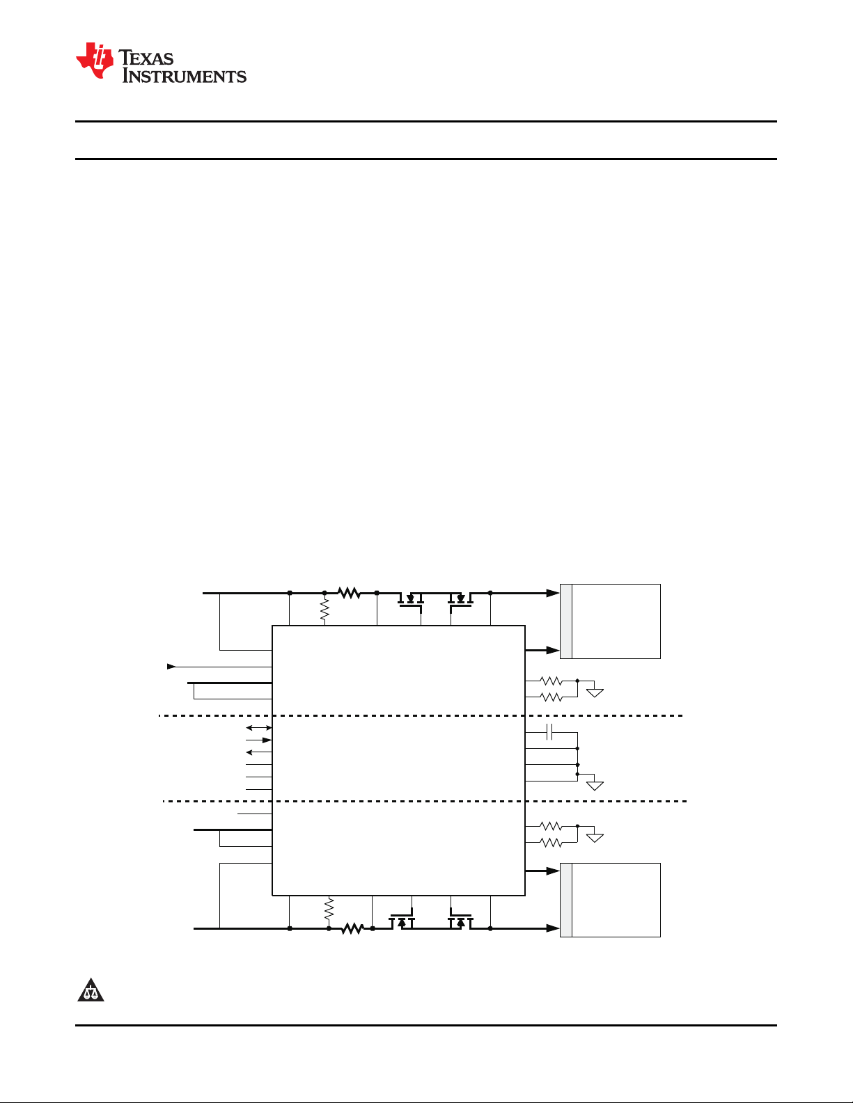
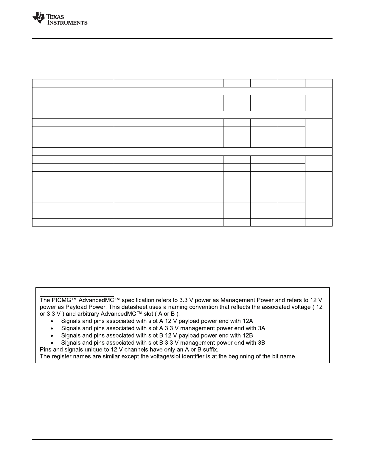
AdvancedMC™
12 V
3.3 V
Slot A
Slot B
AdvancedMC™
12 V
3.3 V
TPS2359
www.ti.com
................................................................................................................................................ SLUS792A – FEBRUARY 2008 – REVISED MARCH 2008
TPS2359 Full Featured Dual-Slot AdvancedMC™ Controller
1
FEATURES
2
• ATCA AdvancedMC™ Compliant
• Full Control for Two AdvancedMC™ Modules
• Independent 12-V Current Limit and Fast Trip
• 3.3-V and 12-V FET ORing for MicroTCA™
• Internal 3.3-V Current Limit and ORing
• Power Good and Fault Reporting Through I2C
• I2C Programmable Fault Times and Current
Limits
• FET Status Bits for all Channels
• 36-Pin PQFN Package
APPLICATIONS
• ATCA Carrier Boards
• MicroTCA™ Power Modules
• AdvancedMC™ Slots
• Systems Using 12 V and 3.3 V
• Base Stations
DESCRIPTION
The TPS2359 dual-slot hot-plug controllers perform
all necessary power interface functions for two
AdvancedMC™ (Advanced Mezzanine Card)
modules.
Two fully integrated 3.3-V channels provide inrush
control, over-current protection, and FET ORing. Two
12-V channels provide the same functions using
external FETs and sense resistors. The 3.3-V current
limits are factory set to AdvancedMC™ compliant
levels and the 12-V current limits are programmed
using external sense resistors. The accurate current
sense comparators of the TPS2359 satisfy the narrow
ATCA™ AdvancedMC™ current limit requirements.
TPS2359 Application Diagram
1
2 AdvancedMC, MicroTCA are trademarks of PICMG.
PRODUCTION DATA information is current as of publication date.
Products conform to specifications per the terms of the Texas
Instruments standard warranty. Production processing does not
necessarily include testing of all parameters.
Copyright © 2008, Texas Instruments Incorporated
Please be aware that an important notice concerning availability, standard warranty, and use in critical applications of
Texas Instruments semiconductor products and disclaimers thereto appears at the end of this data sheet.
Copyright © 2008, Texas Instruments Incorporated
TPS2359
SLUS792A – FEBRUARY 2008 – REVISED MARCH 2008 ................................................................................................................................................
ORDERING INFORMATION
DEVICE TEMPERATURE PACKAGE
TPS2359 -40 ° C to 85 ° C QFN36 TPS2359RHH
(1) Add an R suffix to the device type for tape and reel.
(2) For the most current package and ordering information see the Package Option Addendum at the end of this document or see the TI
Web site at www.ti.com .
ABSOLUTE MAXIMUM RATINGS
(1)
(1)
(2)
ORDERING INFORMATION
www.ti.com
over operating free-air temperature range (unless otherwise noted)
PARAMETER VALUE UNIT
PASSx, BLKx 0 to 30
IN12x; OUT12x; SENPx; SENMx; SETx; IRPT 0 to 17
IN3x; OUT3x; EN3x; VDDx; SUMx; SDA, SCL 0 to 5 V
AGND, GNDx -0.3 to 0.3
A0, A1, A2 0 to VINT
SUMx 5
VINT -1 to 1 mA
OUT3x Internally limited
(1) Stresses beyond those listed under absolute maximum ratings may cause permanent damage to the device. These are stress ratings
only. Functional operation of the device under any conditions beyond those indicated under recommended operating conditions is
neither implied nor guaranteed. Exposure to absolute maximum rated conditions for extended periods of time may affect device
reliability.
ELECTROSTATIC DISCHARGE (ESD) PROTECTION
TEST METHOD MIN UNITS
Human Body Model (HBM) 2
Charged Device model (CDM) 0.5
DISSIPATION RATINGS
PACKAGE θ JA - Low-k ( ° C/W) θ JA - High-k ( ° C/W) TA= 85 ° C POWER RATING (mW)
36 QFN 35
RECOMMENDED OPERATING CONDITIONS
over operating free-air temperature range (unless otherwise noted)
PARAMETER MIN TYP MAX UNIT
V
IN12x
V
IN3x
V
VDD3x,3
I
OUT3x
I
SUMx
T
J
Payload power input voltage 8.5 12 15
Management power input voltage 3 3.3 4 V
Management power supply voltage 3 3.3 4
Management power output current 165 mA
Summing pin current 100 1000
PASSx pin board leakage current -1 1
VINT bypass capacitance 1 10 250 nF
Operating junction temperature range -40 125 ° C
kV
µ A
2 Submit Documentation Feedback Copyright © 2008, Texas Instruments Incorporated
Product Folder Link(s): TPS2359

TPS2359
www.ti.com
ELECTRICAL CHARACTERISTICS
................................................................................................................................................ SLUS792A – FEBRUARY 2008 – REVISED MARCH 2008
(1)
IN3A = IN3B = VDD3A = VDD3B = 3.3 V. IN12A = IN12B = SENPA = SENPB = SENMA = SENMB = SETPA = SETPB = 12
V. EN3A = EN3B = AGND = GNDA = GNDB = 0 V. SUM12A = SUM12B = 6.8 k Ω to ground. SUM3A = SUM3B = 3.3 k Ω to
ground. All other pins open. All I2C bits at default values. Over free air temperature operating range and all voltages
referenced to AGND, unless otherwise noted. over operating free-air temperature range (unless otherwise noted)
PARAMETER CONDITIONS MIN TYP MAX UNITS
ENABLE Inputs
Threshold voltage, falling edge 1.2 1.3 1.4 V
Hysteresis
Pullup current2 EN3x = 0 V 5 8 15
Input bias current EN3x = 5 V 1 5
3.3-V turn off time EN3x deasserts to V
12-V turn off time 20
VINT
Output voltage 0 < I
Power GOOD Outputs
Threshold voltage V
Hysteresis mV
Fault Timer
Minimum fault time 3xFT[4:0] = 12xFT[4:0] = 00001B 1
Fault time bit weight 0.5
Timer duty cycle = (fault time) / (retry period) 1.4% 1.5% 1.6%
12-V Summing node
Input referred offset – 2 2 mV
Summing threshold 12xCL[3:0] = 1111B, VPASSx = 15 V 0.66 0.675 0.69 V
Leakage current VSETx = VSENMx – 10 mV 1 µ A
12-V Current limit
Current limit threshold and measure V
Sink current in current limit V
Fast trip threshold Measure V
Fast turn-off delay
Bleed down resistance V
Bleed down threshold 75 100 130 mV
Timer start threshold V
(1) When setting an address bit to a logic 1 the pin should be connected to VINT.
(2) Not production tested.
(2)
EN3x deasserts to V
Q
= 35 nF
GATE
< 50 µ A 2 2.3 2.8 V
VINT
< 1.0 V, C
OUT3x
< 1.0 V, C
OUT12x
= 0 µ F 10
OUT
= 0 µ F,
OUT
20 50 80 mV
12xPG, falling OUT12x 10.2 10.5 10.8
3xPG, falling OUT3x 2.7 2.8 2.9
12xPG, measured at OUT12x 130
3xPG, measured at OUT3x 50
V
= 10.8 – 13.2 V, V
SENMx
mV, measure V
R
= 6.8 k Ω , R
SUMx
V
= 1 V, V
SUMx
(2)
20-mV overdrive, C
OUT
PASSx
SENPx
= 6 V 1.1 1.6 2.1 k Ω
– V
INx
– V
SETx
= 422 Ω , increase I
SETx
– V
SENPx
= 12 V, measure I
PASSx
– V
SENMx
PASSx
when fault timer starts 5 6 7 V
SENPx
SENMx
SENMx
= 0 pF, t
= V
when V
+ 50
SENMx
LOADx
= 15 47.5 50 52.5 mV
PASSx
PASSx
20 40 µ A
80 100 120 mV
p50-50
200 300 ns
µ A
µ s
ms
Copyright © 2008, Texas Instruments Incorporated Submit Documentation Feedback 3
Product Folder Link(s): TPS2359
TPS2359
SLUS792A – FEBRUARY 2008 – REVISED MARCH 2008 ................................................................................................................................................
www.ti.com
ELECTRICAL CHARACTERISTICS (continued)
IN3A = IN3B = VDD3A = VDD3B = 3.3 V. IN12A = IN12B = SENPA = SENPB = SENMA = SENMB = SETPA = SETPB = 12
V. EN3A = EN3B = AGND = GNDA = GNDB = 0 V. SUM12A = SUM12B = 6.8 k Ω to ground. SUM3A = SUM3B = 3.3 k Ω to
ground. All other pins open. All I2C bits at default values. Over free air temperature operating range and all voltages
referenced to AGND, unless otherwise noted. over operating free-air temperature range (unless otherwise noted)
PARAMETER CONDITIONS MIN TYP MAX UNITS
12-V UVLO
UVLO rising IN12x rising 8.1 8.5 8.9
UVLO hysteresis IN12x falling 0.44 0.5 0.59
12-V BLOCKING
Turn-on threshold Measure V
Turn-off threshold Measure V
Turn-off delay
(3)
20-mV overdrive, C
12-V Gate drivers (PASSx, BLKx)
Output voltage V
Sourcing current V
Sinking current
= V
INx
OUTx
= V
IN12x
Fast turnoff, V
Sustained, V
Pulldown resistance In OTSD (at 150 ° C) 14 20 26 k Ω
Fast turnoff duration
Safety gate pulldown
Startup time
(3)
(3)
(3)
IRF3710, slew S or D 15 V in 1 ms 1.25 V
IN12x rising to PASSx and BLKx sourcing 0.25 ms
3.3-V Summing node
Summing threshold 655 675 695 mV
3.3-V Current limit
On resistance I
Current limit R
= 150 mA 290 500 m Ω
OUT3x
= 3.3 k Ω , V
SUM3x
Fast trip threshold 240 300 400
Fast turn-off delay
Bleed down resistance V
(3)
I
= 400 mA, t
OUT3x
= 1.65 V 280 400 500 Ω
OUT3x
Bleed down threshold 75 100 130 mV
3.3-V UVLO
UVLO rising IN3x rising 2.65 2.75 2.85 V
UVLO hysteresis IN3x falling 200 240 300 mV
3.3-V Blocking
Turn-on threshold Measure V
Turn-off threshold Measure V
V
= 3.3 V, V
IN3x
ORing turn-on delay 300 350 µ s
GND, 3ORON = 1. Remove 3.5 V from OUT3x.
Measure time from V
3.2 V
Fast turnoff delay
(3)
20 mV overdrive, t
(3) Not production tested.
– V
SENPx
SENPx
OUTx
– V
OUTx
= 0 pF, t
BLKx
p50-50
5 10 15
– 6 – 3 0
200 300 ns
= 10 V 21.5 23 24.5 V
= 10 V, V
OUT12x
= V
PASSx
PASSx
BLKx
= V
BLKx
= V
PASSx
= 17 V 20 30 40 µ A
BLKx
= 14 V 0.5 1 A
= 4 – 25 V 10 14 20 mA
5 10 15 ms
= 0 V 170 195 225
OUT3x
p50-50
– V
IN3x
OUT3x
– V
IN3x
OUT3x
= 3.5 V, OUT3x = 100 Ω to
OUT3x
thru 2.9 V to V
OUT3x
p50-50
=
OUT3x
5 10 15
– 6 – 3 0
750 1300 ns
250 350 ns
V
mV
mA
mV
4 Submit Documentation Feedback Copyright © 2008, Texas Instruments Incorporated
Product Folder Link(s): TPS2359
SIGNAL ANDPINNAMING
TPS2359
www.ti.com
................................................................................................................................................ SLUS792A – FEBRUARY 2008 – REVISED MARCH 2008
ELECTRICAL CHARACTERISTICS (continued)
IN3A = IN3B = VDD3A = VDD3B = 3.3 V. IN12A = IN12B = SENPA = SENPB = SENMA = SENMB = SETPA = SETPB = 12
V. EN3A = EN3B = AGND = GNDA = GNDB = 0 V. SUM12A = SUM12B = 6.8 k Ω to ground. SUM3A = SUM3B = 3.3 k Ω to
ground. All other pins open. All I2C bits at default values. Over free air temperature operating range and all voltages
referenced to AGND, unless otherwise noted. over operating free-air temperature range (unless otherwise noted)
PARAMETER CONDITIONS MIN TYP MAX UNITS
Supply Currents (I
All channels enabled I
All channels disabled 2.0 2.8
Thermal Shutdown
Whole-chip shutdown temperature
3.3-V channel shutdown
temperature
Hysteresis
(4)
(4)
Serial Interface (SDA, SCL, A0 – 2, IRPT
Lower logic threshold A0 – A2 0.33 0.35 0.37
Upper logic threshold A0 – A2 1.32 1.35 1.38
Input pullup resistance A0 – A2, V
Input pulldown resistance A0 – A2, V
Input open-circuit voltage IAx = 0 V 0.5 0.8 1.0
Threshold voltage, rising SDA, SCL 2.3 V
Threshold voltage, falling SDA, SCL 1.0
Hysteresis
(4)
Leakage SDA, IRPT 1 mA
(4) Not production tested.
+ I
INx
+ I
SENPx
SENMx
(4)
+ I
SETx
OUT3A
TJrising, I
TJrising, I
+ I
)
VDDx
= I
= 0 3.1 4
OUT3B
= I
OUT3A
or I
OUT3A
= 0 140 150
OUT3B
in current limit 130 140 ° C
OUT3B
Whole chip or 3.3-V channel 10
= 0 V 400 700 1000
Ax
= VINT 200 350 550
Ax
SDA, SCL 165 mV
mA
V
k Ω
Copyright © 2008, Texas Instruments Incorporated Submit Documentation Feedback 5
Signal and Pin Naming Convention
Product Folder Link(s): TPS2359
+
+
+
+
+
R
SEN SE
100mv
vthoc - 675 mv nominal
Q
Pump
Vcp
~25 V
Fault
Timer
Vcp
30 uA
12dis
10 us
R
SUM
6800 W
FLT
10 mv
-3 mv
SQQ
R
PG\
10 us
pgat\
ogat
ogat
OUT12xBLKxPASSxSETx SENMxSENPx
100
us
12xIN
OUT
vpg
OUT pgat\
oren
+
30 uA
R
SET
EN\
SUM12x
TPS2359
SLUS792A – FEBRUARY 2008 – REVISED MARCH 2008 ................................................................................................................................................
www.ti.com
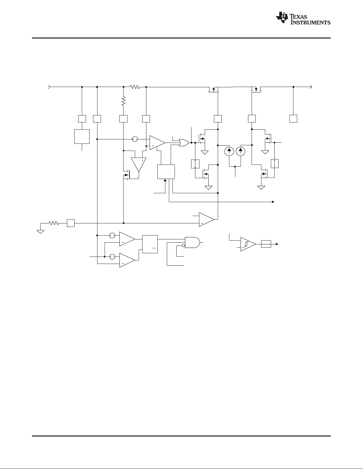
DEVICE INFORMATION
TPS2359 BLOCK DIAGRAMS
Figure 1. Payload Power Channel (two channels per device)
6 Submit Documentation Feedback Copyright © 2008, Texas Instruments Incorporated
Product Folder Link(s): TPS2359
+
+
+
+
0.1 W
30 mv
vthoc - [ 675 mv nominal ]
Fault
Timer
vcpx
R
SU M
3300
FLT \ to I2C
10 mv
-3 mv
SQQ
R
PG\ to I2C
OUT3xIN3x
OUT3x
+
30 uA
245 W
Q
Pump
vcpx
~25 v
VDD3x
+
30 us
2.8 V
gat
EN3x
gat
en
en
30 us
12dis
Control
fromI
2
C
SUM3x
Selector
IN12A
en
V
INT
IN12B
IN3A
IN3B
OUT12A
OUT12B
OUT3A
OUT3B
PREREG
Trim
NVM
SDA
AGND
GNDA
2.2V
POR
por
GNDB
I2C
SCL
A0-2
IRPT\
TPS2359
www.ti.com
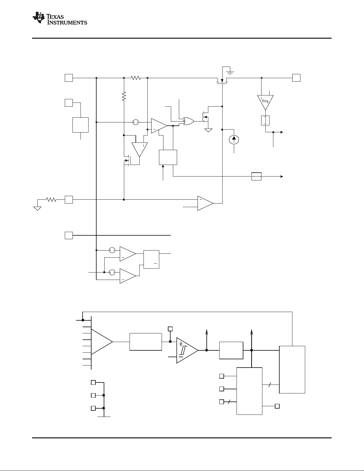
................................................................................................................................................ SLUS792A – FEBRUARY 2008 – REVISED MARCH 2008
Management Power Channel (two channels per device)
Common Circuitry
Copyright © 2008, Texas Instruments Incorporated Submit Documentation Feedback 7
Product Folder Link(s): TPS2359
IN12A
SENPA
SENMA
SDA
VDD3A
12B
3A
SETA
VINT
SUM12A
IN3A
A2
SCL
SUM3A
IN12B
SENPB
SENMB
PASSB
SETB
IRPT\
BLKB
IN3B
SUM3B
OUT12B
VDD3B
OUT3A
A1
OUT3BSUM12B
BLKA
OUT12A
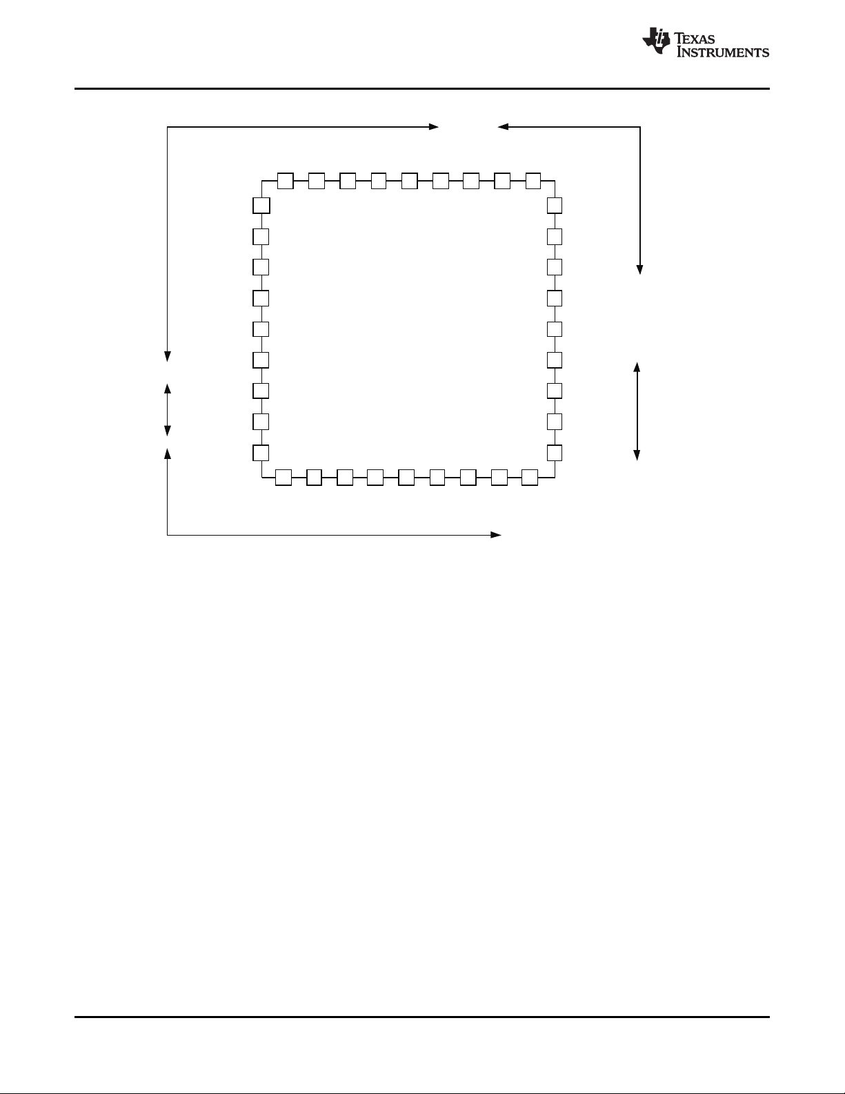
36 Pin QFN
PASSA
GNDB
1
6
5
4
3
2
9
8
7
10 11 12 13 14 15 16 17 18
27
22
23
24
25
26
19
20
21
36 35 34 33 32 31 30 29 28
EN3B
A0
EN3A
12A
3B
I2C
AGND
GNDA
TPS2359
SLUS792A – FEBRUARY 2008 – REVISED MARCH 2008 ................................................................................................................................................
www.ti.com
Top View 36-Pin QFN
8 Submit Documentation Feedback Copyright © 2008, Texas Instruments Incorporated
Product Folder Link(s): TPS2359

TPS2359
www.ti.com
................................................................................................................................................ SLUS792A – FEBRUARY 2008 – REVISED MARCH 2008
TPS2359 TERMINAL FUNCTIONS
PIN # NAME TYPE DESCRIPTION
1 IN12A V
DD
2 SENPA I 12A input sense
3 SETA I 12A current limit set
4 SENMA I 12A current limit sense
5 VINT I/O Bypass capacitor connection point for internal supply, pullup for A0 – A2
6 SUM12A I/O 12A summing node
7 SDA I/O Serial data input/output
8 SCL I Serial data clock
9 SUM12B I/O 12B summing node
10 BLKB O 12B blocking transistor gate drive
11 OUT12B I/O 12B output
12 GNDB GND 12B power ground
13 PASSB O 12B pass transistor gate drive
14 SENMB I 12B current limit sense
15 SETB I 12B current limit set
16 SENPB I 12B input sense
17 IN12B V
18 IN3B V
DD
DD
19 OUT3B I/O 3B output
20 A1 I I2C address programming bit, LSB+1
21 SUM3B I/O 3B summing node
22 VDD3B V
DD
23 AGND GND Analog ground
24 IRPT O Active low interrupt, asserts when a PG deasserts or when a FLT\ asserts
25 SUM3A I/O 3A summing node
26 A2 I I2C address programming bit, LSB+2
27 OUT3A I/O 3A output
28 IN3A V
29 VDD3A V
DD
DD
30 EN3B I 3B enable, active high
31 EN3A I 3A enable, active high
32 PASSA O 12A pass transistor gate drive
33 GNDA GND 12A power ground
34 OUT12A I/O 12A output
35 BLKA O 12A blocking transistor gate drive
36 A0 I I2C address programming bit, LSB
12A input
12B input
3B input
3B charge pump input
3A input
3A charge pump input
Copyright © 2008, Texas Instruments Incorporated Submit Documentation Feedback 9
Product Folder Link(s): TPS2359

TPS2359
SLUS792A – FEBRUARY 2008 – REVISED MARCH 2008 ................................................................................................................................................
www.ti.com
DETAILED PIN DESCRIPTION
A0, A1, A2 These three pins select one of 27 unique I2C addresses for address of the TPS2359. Each pin may
be tied to ground, tied to the VINT pin, or left open. See TPS2359 I2C Interface section for details.
AGND Ground pin for analog circuitry inside the TPS2359.
BLKx Gate drive pin for the 12x channel BLK FET. This pin sources 30 µ A to turn the FET on. An internal clamp
prevents this pin from rising more than 14.5 V above OUT12x. Setting the ORENx bit low holds the BLKx pin
low.
EN3x Active-high enable input. Pulling this pin low turns off channel 3x by pulling the gate of the internal pass
FET to GND. An internal 200-k Ω resistor pulls this pin up to VINTwhen disconnected.
GNDx Ground pin for power circuitry associated with the 12x channel. These pins should connect to a ground
plane shared with the AGND pin.
IN12x Supply pin for channel 12x internal circuitry.
IN3x Supply pin for channel 3x internal pass FET.
IRPT Open drain output that pulls low when internal circuitry sets any of the eight status bits in Register 7.
Reading Register 7 restores IRPT to its high-Z state.
OUT12x Senses the output voltage of the channel 12x path.
OUT3x Output of the channel 3x internal pass FET.
PASSx Gate drive pin for the 12x channel PASS FET. This pin sources 30 µ A to turn the FET on. An internal
clamps prevents this pin from rising more than 14.5 V above IN12x.
SCL Serial clock input for the I2C interface. For details of the SCL line, see TPS2359 I2C Interface section.
SDA Bidirectional I2C data line. For details of the SDA line, see TPS2359 I2C Interface section for details.
SENMx Senses the voltage on the low side of the channel 12x current sense resistor.
SENPx Senses the voltage on the high side of the channel 12x current sense resistor.
SETx A resistor connected from this pin to SENPx sets the current limit level in conjunction with the current
sense resistor and the resistor connected to the SUM12x pin, as described in 12-V thresholds – setting current
limit and fast over current trip section.
SUMx A resistor connected from this pin to ground forms part of the channel x current limit. As the current
delivered to the load increases, so does the voltage on this pin. When the voltage on this pin reaches a threshold
(by default 675 mV), the current limit amplifier acts to prevent the current from further increasing.
VDD3x Supply pin for channel3x internal circuitry.
VINT This pin connects to the internal 2.35-V rail. A 0.1- µ F capacitor must be connected from this pin to ground.
One can connect the A0 – A2 pins to this supply to pull them high, but no other external circuitry should connect to
VINT.
10 Submit Documentation Feedback Copyright © 2008, Texas Instruments Incorporated
Product Folder Link(s): TPS2359
12V VDD vs IDD @ 25C
2.1
2.15
2.2
2.25
2.3
2.35
2.4
2.45
10 11 12 13 14
VDD
IDD (mA)
3V Channel ORing Turn On Threshold
8.00
9.00
10.00
11.00
12.00
-50 0 50 100 150
Temperature De grees C
mV
3V Channel ORing Turn Off Thre shold
-5.00
-4.00
-3.00
-2.00
-1.00
0.00
-50 0 50 100 150
Temperature C Degree s
mV
12 V Fast Curr ent Limit Thres hold
50.00
50.20
50.40
50.60
50.80
51.00
-50 0 50 100 150
Temperature De grees C
mV
3.3V IDD Vs Tem pe rature
0.2
0.21
0.22
0.23
0.24
0.25
0.26
-50 0 50 100 150
Temperature Degree s C
IDD (mA)
12V Channel ORing Turn Off Thre shold
-5.0 0
-4.0 0
-3.0 0
-2.0 0
-1.00
0.00
-50 0 50 100 150
Temperature De gree C
mV
12V Cur re nt (mA) Vs Te mper ature
2
2.1
2.2
2.3
2.4
-50 0 50 100 150
Temperature Degree s C
Current (mA)
6
12V Channel ORing Turn On Thr eshold
8.00
8.50
9.00
9.50
10.00
10.50
11.0 0
11.50
12.00
-50 0 50 10 0 150
Temperature De grees C
mV
TPS2359
www.ti.com
................................................................................................................................................ SLUS792A – FEBRUARY 2008 – REVISED MARCH 2008
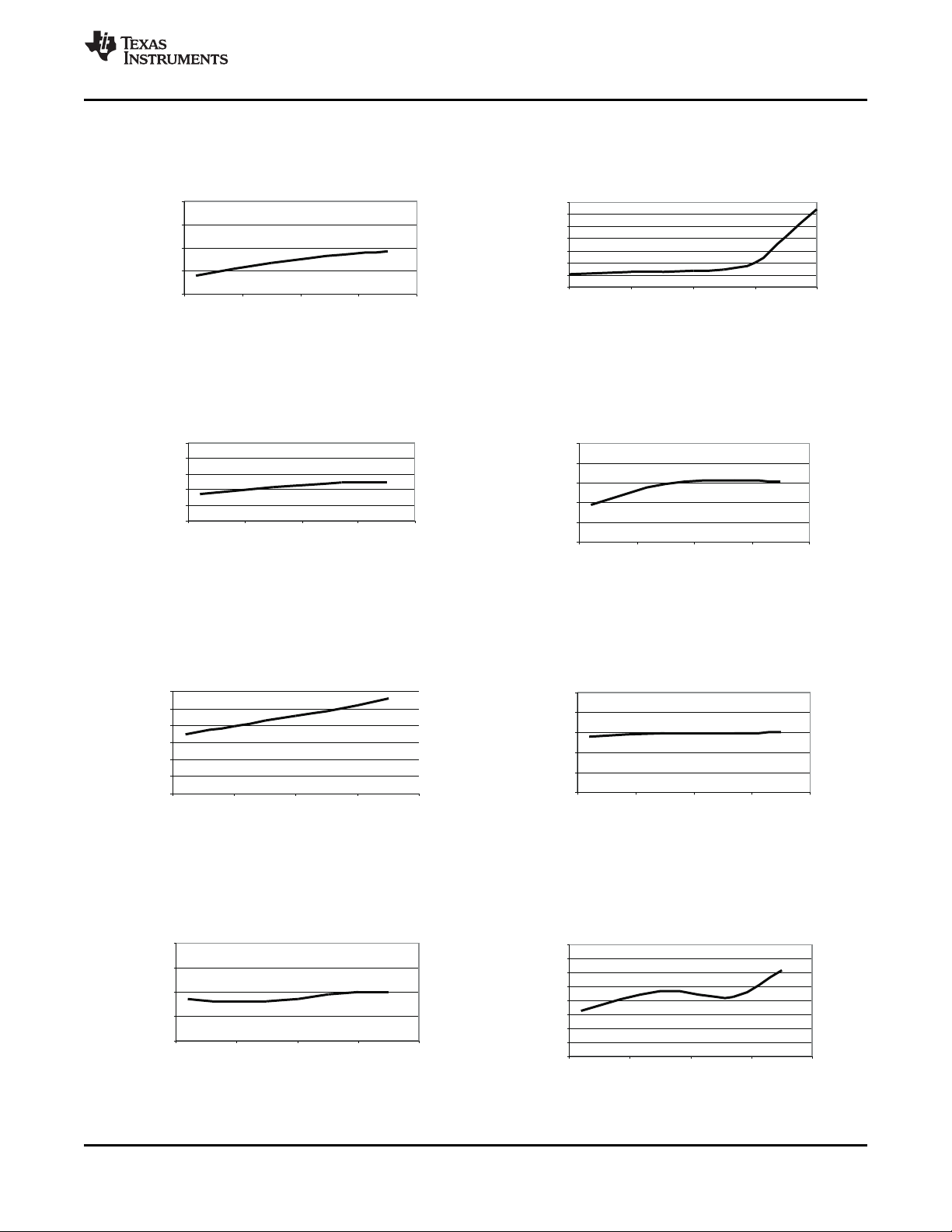
TYPICAL CHARACTERISTICS
Figure 2. Figure 3.
Figure 4. Figure 5.
Figure 6. Figure 7.
Figure 8. Figure 9.
Copyright © 2008, Texas Instruments Incorporated Submit Documentation Feedback 11
Product Folder Link(s): TPS2359
TPS2359
SLUS792A – FEBRUARY 2008 – REVISED MARCH 2008 ................................................................................................................................................
TYPICAL CHARACTERISTICS (continued)
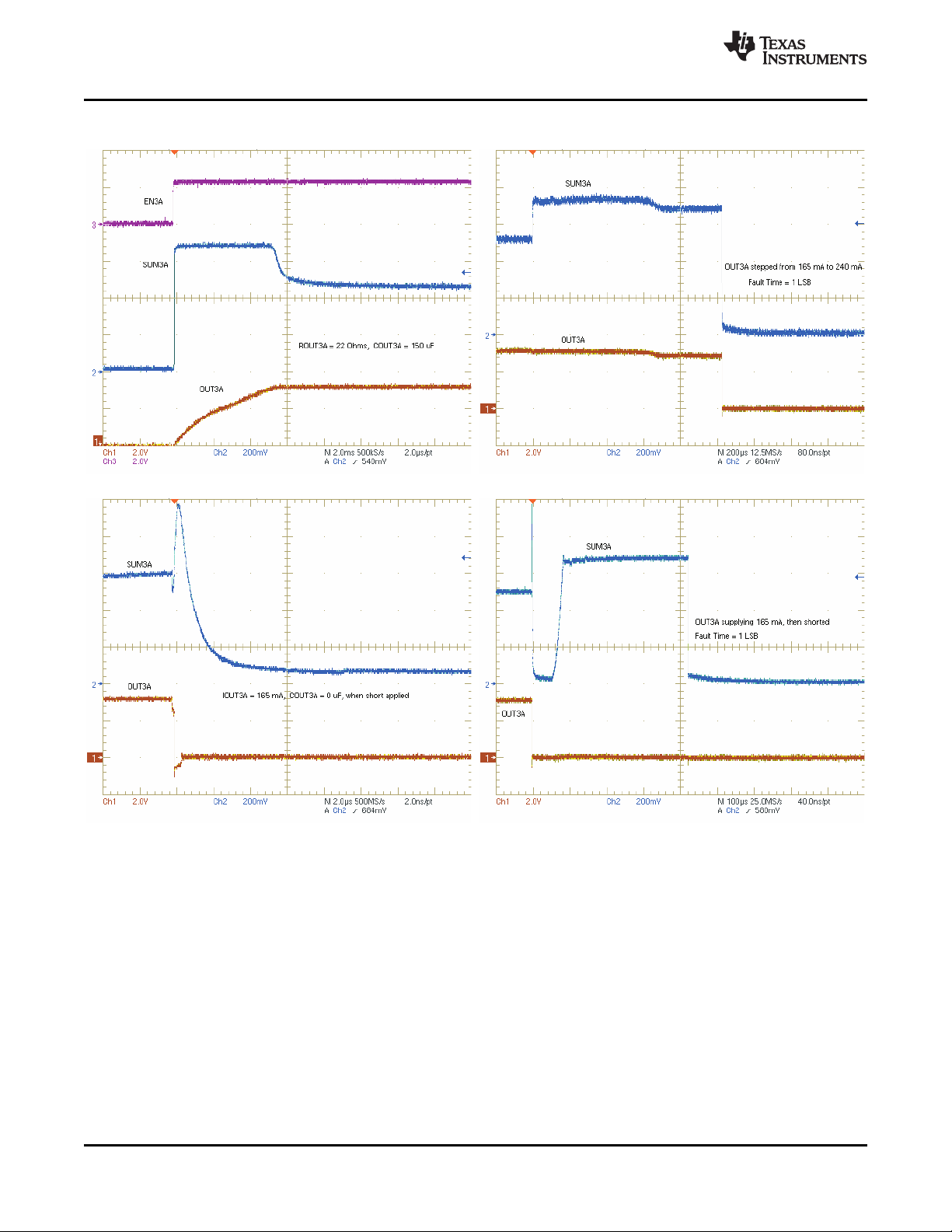
Figure 10. OUT3A Startup Into 22- Ω (150 mA) 150- µ F Load Figure 11. OUT3A Load Stepped from 165 mA to 240 mA
www.ti.com
Figure 12. OUT3A Short Circuit Under Full Load (165 mA) Figure 13. OUT3A Short Circuit Under Full Load (165 mA)
12 Submit Documentation Feedback Copyright © 2008, Texas Instruments Incorporated
Zoom View Wide View
Product Folder Link(s): TPS2359
TPS2359
www.ti.com
................................................................................................................................................ SLUS792A – FEBRUARY 2008 – REVISED MARCH 2008
TYPICAL CHARACTERISTICS (continued)
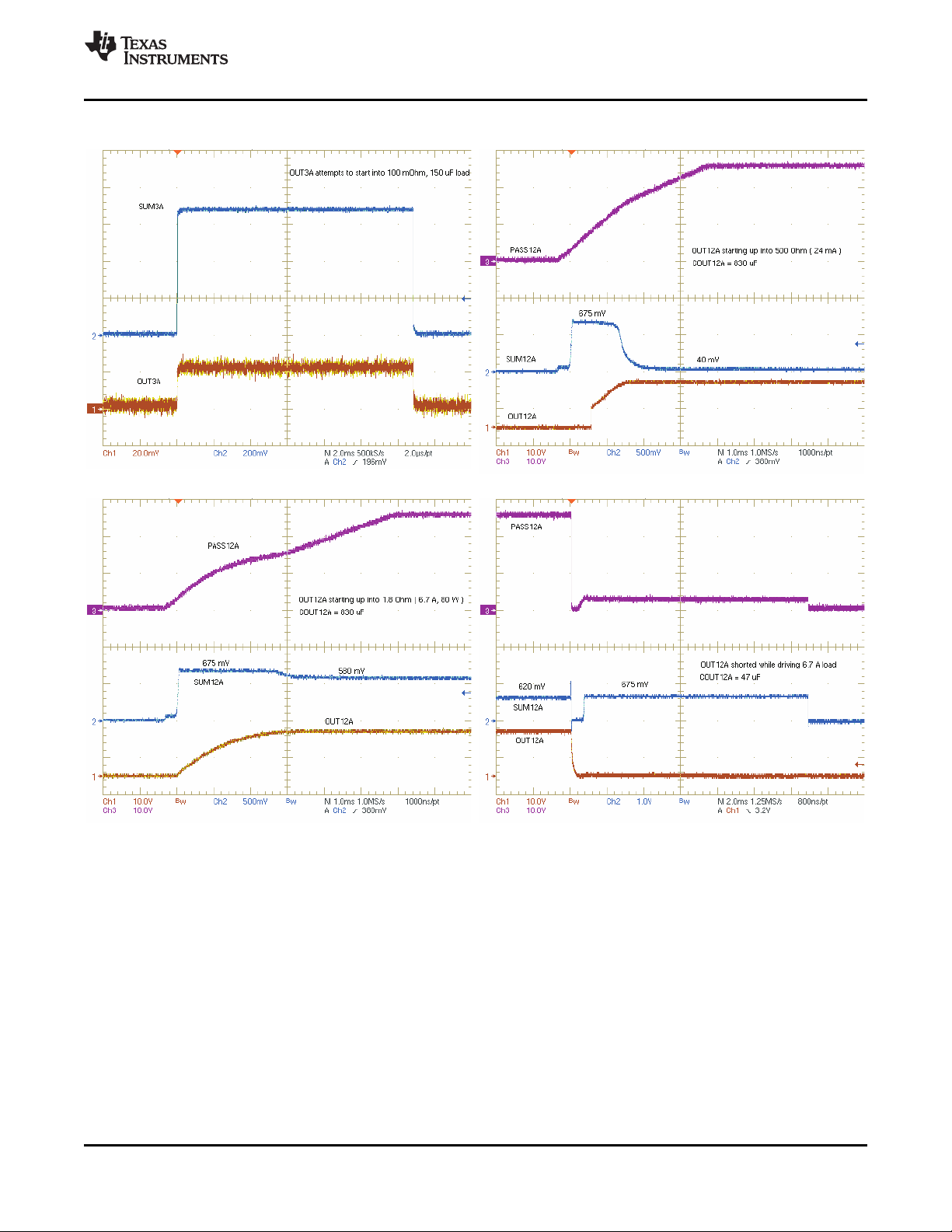
Figure 14. OUT3A Startup Into Short Circuit Figure 15. OUT12A Startup Into 500- Ω , 830- µ F Load
Figure 16. OUT12A Startup Into 80-Watt, 830- µ F Load Figure 17. OUT12A Short Circuit Under Full Load (6.7 A)
Copyright © 2008, Texas Instruments Incorporated Submit Documentation Feedback 13
Product Folder Link(s): TPS2359
Wide View
TPS2359
SLUS792A – FEBRUARY 2008 – REVISED MARCH 2008 ................................................................................................................................................
www.ti.com
TYPICAL CHARACTERISTICS (continued)
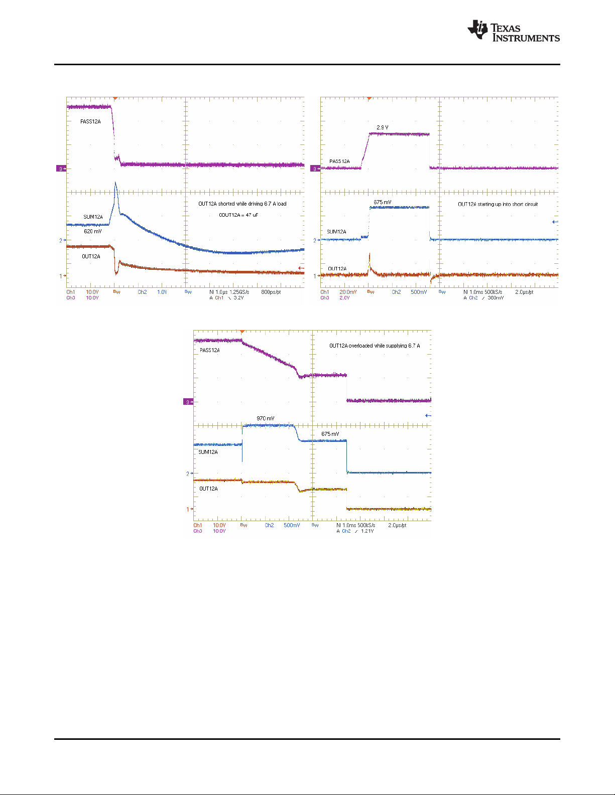
Figure 18. OUT12A Short Circuit Under Full Load (6.7 A) Figure 19. OUT12A Startup Into Short Circuit
Zoom View
Figure 20. OUT12A Overloaded While Supplying 6.7 A
14 Submit Documentation Feedback Copyright © 2008, Texas Instruments Incorporated
Product Folder Link(s): TPS2359
TPS2359
www.ti.com
................................................................................................................................................ SLUS792A – FEBRUARY 2008 – REVISED MARCH 2008
REFERENCE INFORMATION
The TPS2359 has been designed to simplify compliance with the PICMG-AMC.R2.0 and PICMG-MTCA.0
specifications. These specifications were developed by the PCI Industrial Computer Manufacturers Group
(PICMG). These two specifications are derivations of the PICMG-ATCA (Advanced Telecommunication
Computing Architecture) specification originally released in December, 2002.
PICMG-AMC Highlights
• AMC - Advanced Mezzanine Cards
• Designed to Plug into ATCA Carrier Boards
• AdvancedMC™ Focuses on Low Cost
• 1 to 8 AdvancedMC™ per ATCA Carrier Board
• 3.3-V Management Power – Maximum Current Draw of 150 mA
• 12-V Payload Power – Converted to Required Voltages on AMC
• Maximum 80-W Dissipation per AdvancedMC™
• Hotswap and Current Limiting Must Be Present on Carrier Board
• For Details, see www.picmg.org/v2internal/AdvancedMC.htm
PICMG-MTCA Highlights
• MTCA – MicroTelecommunications Computing Architecture
• Architecture for Using AMCs Without an ATCA Carrier Board
• Up to 12 AMCs per System, Plus Two MCHs, Plus Two CUs
• Focuses on Low Cost
• All functions of ATCA Carrier Board Must Be Provided
• MicroTCA is Also Known as MTCA, mTCA, or uTCA For Details, see
www.picmg.org/v2internal/microTCA.htm
Control and Status Registers
Ten 8 bit registers are used to control and read the status of the TPS2359. Registers 0 and 1 control the 12A
channel and register 2 controls the 3A channel. Similarly, registers 3 and 4 control the 12B channel and register
5 controls the 3B channel. Register 6 contains eight general configuration bits. Read-only registers 7, 8, and 9
report back system status to the I2C controller. All ten registers use the I2C protocol and are organized as
follows:
Table 1. Top Level Register Functions
REG R/W SLOT VOLTAGE FUNCTION
0 R/W A 12 Set current limit, power good threshold, and OR functions of 12A.
1 R/W A 12 Set fault time, enable, and bleed down functions of 12A.
2 R/W A 3.3 Set fault time, enable, and bleed down functions of 3A.
3 R/W B 12 Set current limit, power good threshold, and OR functions of 12B.
4 R/W B 12 Set fault time, enable, and bleed down functions of 12B.
5 R/W B 3.3 Set fault time, enable, and bleed down functions of 3B.
6 R/W A, B 3.3, 12 System configuration controls.
7 R A, B 3.3, 12 Fault and PG outputs for 3A, 12A, 3B, 12B – these bits set IRPT.
8 R A, B 12 Over current and fast trip latches for 3A, 12A, 3B, 12B.
9 R A, B 3.3, 12 Channel status indicators for 3A, 12A, 3B, 12B.
Copyright © 2008, Texas Instruments Incorporated Submit Documentation Feedback 15
Product Folder Link(s): TPS2359

TPS2359
SLUS792A – FEBRUARY 2008 – REVISED MARCH 2008 ................................................................................................................................................
Summary of Registers
Table 2. Summary of Registers
BIT NAME DEFAULT DESCRIPTION
Register 0 Read/Write channel 12A configuration
0 12ACL0 1 Clearing bit reduces 12A current limit & fast threshold by 5%.
1 12ACL1 1 Clearing bit reduces 12A current limit & fast threshold by 10%.
2 12ACL2 1 Clearing bit reduces 12A current limit & fast threshold by 20%.
3 12ACL3 1 Clearing bit reduces 12A current limit & fast threshold by 40%.
4 12APG0 1 Clearing bit reduces 12A power good threshold by 600mV.
5 12APG1 1 Clearing bit reduces 12A power good threshold by 1.2 V.
6 12AHP 0 Setting bit shifts 12A OR VTURNOFF from – 3 mV to +3 mV nominal.
7 12AOR 1 Clearing bit turns off 12A ORing FET by pulling BLKA low.
Register 1 Read/Write channel 12A configuration
0 12AFT0 1 Setting bit increases 12A fault time by 0.5 ms.
1 12AFT1 0 Setting bit increases 12A fault time by 1 ms.
2 12AFT2 0 Setting bit increases 12A fault time by 2 ms.
3 12AFT3 0 Setting bit increases 12A fault time by 4 ms.
4 12AFT4 0 Setting bit increases 12A fault time by 8 ms.
5 12AEN 0 Clearing bit disables 12A by pulling PASSA and BLKA to 0 V.
6 12AUV 0 Setting bit prevents enabling unless OUT12A < bleed down threshold.
7 12ADS 0 Clearing bit disconnects OUT12A bleed down resistor.
Register 2 Read/Write channel 3A configuration
0 3AFT0 1 Setting bit increases 3A fault time by 0.5 ms.
1 3AFT1 0 Setting bit increases 3A fault time by 1 ms.
2 3AFT2 0 Setting bit increases 3A fault time by 2 ms.
3 3AFT3 0 Setting bit increases 3A fault time by 4 ms.
4 3AFT4 0 Setting bit increases 3A fault time by 8 ms.
5 3AEN 0 Clearing bit disables 3A.
6 3AUV 0 Setting bit prevents enabling unless OUT3A < bleed down threshold.
7 3ADS 0 Clearing bit disconnects OUT3A bleed down resistor.
Register 3 Read/Write channel 12B configuration
0 12BCL0 1 Clearing bit reduces 12B current limit & fast threshold by 5%.
1 12BCL1 1 Clearing bit reduces 12B current limit & fast threshold by 10%.
2 12BCL2 1 Clearing bit reduces 12B current limit & fast threshold by 20%.
3 12BCL3 1 Clearing bit reduces 12B current limit & fast threshold by 40%.
4 12BPG0 1 Clearing bit reduces 12B power good threshold by 600 mV.
5 12BPG1 1 Clearing bit reduces 12B power good threshold by 1.2 V.
6 12BHP 0 Setting bit shifts 12B OR VTURNOFF from – 3 mV to +3 mV nominal.
7 12BOR 1 Clearing bit turns off 12B ORing FET by pulling BLKB low.
Register 4 Read/Write channel 12B configuration
0 12BFT0 1 Setting bit increases 12B fault time by 0.5 ms.
1 12BFT1 0 Setting bit increases 12B fault time by 1 ms.
2 12BFT2 0 Setting bit increases 12B fault time by 2 ms.
3 12BFT3 0 Setting bit increases 12B fault time by 4 ms.
4 12BFT4 0 Setting bit increases 12B fault time by 8 ms.
5 12BEN 0 Clearing bit disables 12B by pulling PASSB and BLKB to 0 V.
6 12BUV 0 Setting bit prevents enabling unless OUT12B < bleed down threshold.
7 12BDS 0 Clearing bit disconnects OUT12B bleed down resistor.
www.ti.com
16 Submit Documentation Feedback Copyright © 2008, Texas Instruments Incorporated
Product Folder Link(s): TPS2359

TPS2359
www.ti.com
................................................................................................................................................ SLUS792A – FEBRUARY 2008 – REVISED MARCH 2008
Table 2. Summary of Registers (continued)
BIT NAME DEFAULT DESCRIPTION
0 12ACL0 1 Clearing bit reduces 12A current limit & fast threshold by 5%.
1 12ACL1 1 Clearing bit reduces 12A current limit & fast threshold by 10%.
2 12ACL2 1 Clearing bit reduces 12A current limit & fast threshold by 20%.
3 12ACL3 1 Clearing bit reduces 12A current limit & fast threshold by 40%.
4 12APG0 1 Clearing bit reduces 12A power good threshold by 600 mV.
5 12APG1 1 Clearing bit reduces 12A power good threshold by 1.2 V.
6 12AHP 0 Setting bit shifts 12A OR VTURNOFF from – 3 mV to +3 mV nominal.
7 12AOR 1 Clearing bit turns off 12A ORing FET by pulling BLKA low.
Register 1 Read/Write channel 12A configuration
0 12AFT0 1 Setting bit increases 12A fault time by 0.5 ms.
1 12AFT1 0 Setting bit increases 12A fault time by 1 ms.
2 12AFT2 0 Setting bit increases 12A fault time by 2 ms.
3 12AFT3 0 Setting bit increases 12A fault time by 4 ms.
4 12AFT4 0 Setting bit increases 12A fault time by 8 ms.
5 12AEN 0 Clearing bit disables 12A by pulling PASSA and BLKA to 0 V.
6 12AUV 0 Setting bit prevents enabling unless OUT12A < bleed down threshold.
7 12ADS 0 Clearing bit disconnects OUT12A bleed down resistor.
Register 2 Read/Write channel 3A configuration
0 3AFT0 1 Setting bit increases 3A fault time by 0.5 ms.
1 3AFT1 0 Setting bit increases 3A fault time by 1 ms.
2 3AFT2 0 Setting bit increases 3A fault time by 2 ms.
3 3AFT3 0 Setting bit increases 3A fault time by 4 ms.
4 3AFT4 0 Setting bit increases 3A fault time by 8 ms.
5 3AEN 0 Clearing bit disables 3A.
6 3AUV 0 Setting bit prevents enabling unless OUT3A < bleed down threshold.
7 3ADS 0 Clearing bit disconnects OUT3A bleed down resistor.
Register 3 Read/Write channel 12B configuration
0 12BCL0 1 Clearing bit reduces 12B current limit & fast threshold by 5%.
1 12BCL1 1 Clearing bit reduces 12B current limit & fast threshold by 10%.
2 12BCL2 1 Clearing bit reduces 12B current limit & fast threshold by 20%.
3 12BCL3 1 Clearing bit reduces 12B current limit & fast threshold by 40%.
4 12BPG0 1 Clearing bit reduces 12B power good threshold by 600 mV.
5 12BPG1 1 Clearing bit reduces 12B power good threshold by 1.2 V.
6 12BHP 0 Setting bit shifts 12B OR VTURNOFF from – 3 mV to +3 mV nominal.
7 12BOR 1 Clearing bit turns off 12B ORing FET by pulling BLKB low.
Register 4 Read/Write channel 12B configuration
0 12BFT0 1 Setting bit increases 12B fault time by 0.5 ms.
1 12BFT1 0 Setting bit increases 12B fault time by 1 ms.
2 12BFT2 0 Setting bit increases 12B fault time by 2 ms.
3 12BFT3 0 Setting bit increases 12B fault time by 4 ms.
4 12BFT4 0 Setting bit increases 12B fault time by 8 ms.
5 12BEN 0 Clearing bit disables 12B by pulling PASSB and BLKB to 0 V.
6 12BUV 0 Setting bit prevents enabling unless OUT12B < bleed down threshold.
7 12BDS 0 Clearing bit disconnects OUT12B bleed down resistor.
7 12BDS 0 Clearing bit disconnects OUT12B bleed down resistor.
Copyright © 2008, Texas Instruments Incorporated Submit Documentation Feedback 17
Product Folder Link(s): TPS2359

TPS2359
SLUS792A – FEBRUARY 2008 – REVISED MARCH 2008 ................................................................................................................................................
www.ti.com
Detailed Description of Registers
Register 0
Table 3. Register 0: Channel 12A Configuration (Read/write)
BIT NAME DEFAULT DESCRIPTION
0 12ACL0 1 Clearing bit reduces 12A current limit & fast threshold by 5%.
1 12ACL1 1 Clearing bit reduces 12A current limit & fast threshold by 10%.
2 12ACL2 1 Clearing bit reduces 12A current limit & fast threshold by 20%.
3 12ACL3 1 Clearing bit reduces 12A current limit & fast threshold by 40%.
4 12APG0 1 Clearing bit reduces 12A power good threshold by 600 mV.
5 12APG1 1 Clearing bit reduces 12A power good threshold by 1.2 V.
6 12AHP 0 Setting bit shifts 12A OR VTURNOFF from – 3 mV to +3 mV nominal.
7 12AOR 1 Clearing bit turns off 12A ORing FET by pulling BLKA low.
12ACL[3:0] These four bits adjusts the 12A current limit and fast trip threshold using the I2C interface. Setting
the bits to 1111B places the 12A current limit at its maximum level, corresponding to 675 mV at SUM12A. The
fast trip threshold then equals 100 mV. Clearing all bits reduces the current limit and fast trip threshold to 25% of
these maximums.
12APG[1:0] These two bits adjust the 12A power good threshold. Setting the bits to 11B places the power good
threshold at its maximum level of 10.5 V . Setting the bits to 00B places the threshold at its minimum level of 8.7
V. The lower thresholds may prove desirable in systems that routinely experience large voltage droops.
12AHP Setting this bit moves the 12A ORing turn off threshold from – 3 mV to +3 mV. A positive threshold
prevents reverse current from flowing through the channel, but it may cause the ORing FET to repeatedly cycle
on-and-off if the load cannot maintain the required positive voltage drop across the combined resistance of the
external FETs and the sense resistor. For further information, see Adjusting Oring Turn Off threshold For High
Power Loads section
12AOR Clearing this bit forces the BLKA pin low, keeping the 12A ORing FET off. Clearing this bit does not
prevent current from flowing through the FET ’ s body diode.
18 Submit Documentation Feedback Copyright © 2008, Texas Instruments Incorporated
Product Folder Link(s): TPS2359

TPS2359
www.ti.com
................................................................................................................................................ SLUS792A – FEBRUARY 2008 – REVISED MARCH 2008
Register 1
Table 4. Register 1: Channel 12A Configuration (Read/write)
BIT NAME DEFAULT DESCRIPTION
0 12AFT0 1 Setting bit increases 12A fault time by 0.5 ms.
1 12AFT1 0 Setting bit increases 12A fault time by 1 ms.
2 12AFT2 0 Setting bit increases 12A fault time by 2 ms.
3 12AFT3 0 Setting bit increases 12A fault time by 4 ms.
4 12AFT4 0 Setting bit increases 12A fault time by 8 ms.
5 12AEN 0 Clearing bit disables 12A by pulling PASSA and BLKA to 0 V.
6 12AUV 0 Setting bit prevents enabling unless OUT12A < bleed down threshold.
7 12ADS 0 Clearing bit disconnects OUT12A bleed down resistor.
12AFT[4:0] These five bits adjust the 12A channel fault time. The least-significant bit has a nominal weight of 0.5
ms, so fault times ranging from 0.5 ms (for code 00001B) to 15.5 ms (for code 11111B) can be programmed. In
general the shortest fault time that fully charges downstream bulk capacitors without generating a fault should be
used. Once the load capacitors have fully charged, the fault time can be reduced to provide faster short circuit
protection. See Setting Fault Time section.
12AEN This bit serves as a master enable for channel 12A. Setting this bit allows the 12A channel to operate
normally. Clearing this bit disables the channel by pulling PASSA and BLKA low.
12AUV Setting this bit prevents channel 12A from turning on until OUT12A falls below the bleed down threshold
of 100 mV. This feature ensures that downstream devices reset by requiring their supply voltage to fall to nearly
zero before the channel can enable them.
12ADS Clearing this bit disconnects the bleed down resistor that otherwise connects from OUT12A to ground.
Systems using redundant power supplies should clear 12ADS to prevent the bleed down resistor from
continuously sinking current.
Copyright © 2008, Texas Instruments Incorporated Submit Documentation Feedback 19
Product Folder Link(s): TPS2359

TPS2359
SLUS792A – FEBRUARY 2008 – REVISED MARCH 2008 ................................................................................................................................................
www.ti.com
Register 2
Table 5. Register 2: Channel 3A Configuration (Read/write)
BIT NAME DEFAULT DESCRIPTION
0 3AFT0 1 Setting bit increases 3A fault time by 0.5 ms.
1 3AFT1 0 Setting bit increases 3A fault time by 1 ms.
2 3AFT2 0 Setting bit increases 3A fault time by 2 ms.
3 3AFT3 0 Setting bit increases 3A fault time by 4 ms.
4 3AFT4 0 Setting bit increases 3A fault time by 8 ms.
5 3AEN 0 Clearing bit disables 3A.
6 3AUV 0 Setting bit prevents enabling unless OUT3A < bleed down threshold.
7 3ADS 0 Clearing bit disconnects OUT3A bleed down resistor.
3AFT[4:0] These five bits adjust the 3A channel fault time. The least-significant bit has a nominal weight of 0.5
ms, so fault times ranging from 0.5 ms (for code 00001B) to 15.5 ms (for code 11111B) can be programmed. In
general the shortest fault time that fully charges downstream bulk capacitors without generating a fault should be
used. See Setting Fault Time section.
3AEN This bit serves as a master enable for channel 3A. Setting this bit allows the 3A channel to operate
normally, provided the EN3A pin is also asserted. Clearing this bit disables the channel by removing gate drive to
the internal pass FET, regardless of the state of the EN3A pin.
3AUV Setting this bit prevents channel 3A from turning on until OUT3A falls below the bleed down threshold of
100 mV. This feature ensures that downstream devices reset by requiring their supply voltage to fall to nearly
zero before the channel can enable them.
3ADS Clearing this bit disconnects the bleed down resistor that otherwise connects from OUT3A to ground.
Systems using redundant power supplies should clear 3ADS to prevent the bleed down resistor from
continuously sinking current.
20 Submit Documentation Feedback Copyright © 2008, Texas Instruments Incorporated
Product Folder Link(s): TPS2359

TPS2359
www.ti.com
................................................................................................................................................ SLUS792A – FEBRUARY 2008 – REVISED MARCH 2008
Register 3
Table 6. Register 3: Channel 12B Configuration (Read/write)
BIT NAME DEFAULT DESCRIPTION
0 12BCL0 1 Clearing bit reduces 12B current limit & fast threshold by 5%.
1 12BCL1 1 Clearing bit reduces 12B current limit & fast threshold by 10%.
2 12BCL2 1 Clearing bit reduces 12B current limit & fast threshold by 20%.
3 12BCL3 1 Clearing bit reduces 12B current limit & fast threshold by 40%.
4 12BPG0 1 Clearing bit reduces 12B power good threshold by 600 mV.
5 12BPG1 1 Clearing bit reduces 12B power good threshold by 1.2 V.
6 12BHP 0 Setting bit shifts 12B OR VTURNOFF from – 3 mV to +3 mV nominal.
7 12BOR 1 Clearing bit turns off 12B ORing FET by pulling BLKB low.
12BCL[3:0] These four bits adjusts the 12B current limit and fast trip threshold using the I2C interface. Setting
the bits to 1111B places the 12B current limit at its maximum level, corresponding to 675 mV at SUM12B. The
fast trip threshold then equals 100 mV. Clearing all bits reduces the current limit and fast trip threshold to 25% of
these maximums.
12BPG[1:0] These two bits adjust the 12B power good threshold. Setting the bits to 11B places the power good
threshold at its maximum level of 10.5 V . Setting the bits to 00B places the threshold at its minimum level of 8.7
V. The lower thresholds may prove desirable in systems that routinely experience large voltage droops.
12BHP Setting this bit moves the 12B ORing turn off threshold from – 3 mV to +3 mV. A positive threshold
prevents reverse current from flowing through the channel, but it may cause the ORing FET to repeatedly cycle
on-and-off if the load cannot maintain the required positive voltage drop across the combined resistance of the
external FETs and the sense resistor. For further information, see Adjusting ORing Turn Off threshold For High
Power Loads section.
12BOR Clearing this bit forces the BLKB pin low, keeping the 12B ORing FET off. Clearing this bit does not
prevent current from flowing through the FET ’ s body diode.
Copyright © 2008, Texas Instruments Incorporated Submit Documentation Feedback 21
Product Folder Link(s): TPS2359

TPS2359
SLUS792A – FEBRUARY 2008 – REVISED MARCH 2008 ................................................................................................................................................
www.ti.com
Register 4
Table 7. Register 4: Channel 12B Configuration (Read/write)
BIT NAME DEFAULT DESCRIPTION
0 12BFT0 1 Setting bit increases 12B fault time by 0.5 ms.
1 12BFT1 0 Setting bit increases 12B fault time by 1 ms.
2 12BFT2 0 Setting bit increases 12B fault time by 2 ms.
3 12BFT3 0 Setting bit increases 12B fault time by 4 ms.
4 12BFT4 0 Setting bit increases 12B fault time by 8 ms.
5 12BEN 0 Clearing bit disables 12B by pulling PASSB and BLKB to 0 V.
6 12BUV 0 Setting bit prevents enabling unless OUT12B < bleed down threshold.
7 12BDS 0 Clearing bit disconnects OUT12B bleed down resistor.
12BFT[4:0] These five bits adjust the 12B channel fault time. The least-significant bit has a nominal weight of 0.5
ms, so fault times ranging from 0.5 ms (for code 00001B) to 15.5 ms (for code 11111B) can be programmed. In
general the shortest fault time that fully charges downstream bulk capacitors without generating a fault should be
used. Once the load capacitors have fully charged, the fault time can be reduced to provide faster short circuit
protection. See Setting Fault Time section.
12BEN This bit serves as a master enable for channel 12B. Setting this bit allows the 12B channel to operate
normally. Clearing this bit disables the channel by pulling PASSB and BLKB low.
12BUV Setting this bit prevents channel 12B from turning on until OUT12B falls below the bleed down threshold
of 100 mV. This feature ensures that downstream devices reset by requiring their supply voltage to fall to nearly
zero before the channel can enable them.
12BDS Clearing this bit disconnects the bleed down resistor that otherwise connects from OUT12B to ground.
Systems using redundant power supplies should clear 12BDS to prevent the bleed down resistor from
continuously sinking current.
22 Submit Documentation Feedback Copyright © 2008, Texas Instruments Incorporated
Product Folder Link(s): TPS2359

TPS2359
www.ti.com
................................................................................................................................................ SLUS792A – FEBRUARY 2008 – REVISED MARCH 2008
Register 5
Table 8. Register 5: Channel 3B Configuration (Read/write)
BIT NAME DEFAULT DESCRIPTION
0 3BFT0 1 Setting bit increases 3B fault time by 0.5 ms.
1 3BFT1 0 Setting bit increases 3B fault time by 1 ms.
2 3BFT2 0 Setting bit increases 3B fault time by 2 ms.
3 3BFT3 0 Setting bit increases 3B fault time by 4 ms.
4 3BFT4 0 Setting bit increases 3B fault time by 8 ms.
5 3BEN 0 Clearing bit disables 3B.
6 3BUV 0 Setting bit prevents enabling unless OUT3B < bleed down threshold.
7 3BDS 0 Clearing bit disconnects OUT3B bleed down resistor.
3BFT[4:0] These five bits adjust the 3B channel fault time. The least-significant bit has a nominal weight of 0.5
ms, so fault times ranging from 0.5 ms (for code 00001B) to 15.5 ms (for code 11111B) can be programmed. In
general the shortest fault time that fully charges downstream bulk capacitors without generating a fault should be
used. See Setting Fault Time section.
3BEN This bit serves as a master enable for channel 3B. Setting this bit allows the 3B channel to operate
normally, provided the EN3B pin is also asserted. Clearing this bit disables the channel by removing gate drive to
the internal pass FET, regardless of the state of the EN3B pin.
3BUV Setting this bit prevents channel 3B from turning on until OUT3B falls below the bleed down threshold of
100 mV. This feature ensures that downstream devices reset by requiring their supply voltage to fall to nearly
zero before the channel can enable them.
3BDS Clearing this bit disconnects the bleed down resistor that otherwise connects from OUT3B to ground.
Systems using redundant power supplies should clear 3BDS to prevent the bleed down resistor from
continuously sinking current.
Copyright © 2008, Texas Instruments Incorporated Submit Documentation Feedback 23
Product Folder Link(s): TPS2359

TPS2359
SLUS792A – FEBRUARY 2008 – REVISED MARCH 2008 ................................................................................................................................................
www.ti.com
Register 6
Table 9. Register 6: System Configuration (Read/write)
BIT NAME DEFAULT DESCRIPTION
0 PPTEST 0 12-V pulldown test pin. Asserting this pulls the PASSx and BLKx pins to 0 V.
1 FLTMODE 0
2 SPARE 0 This bit must always be set to 0.
3 3ORON 0
4 12VNRS 0
5 AIRM 0 Setting this masking bit prevents REG7 bits 3:0 from setting IRPT.
6 BIRM 0 Setting this masking bit prevents REG7 bits 7:4 from setting IRPT.
7 DCC 0
Clearing bit forces channels to latch off after over-current fault. Setting bit allows
channels to automatically attempt restart after fault.
Setting bit enables 3A and 3B to prevent reverse current flow.Clearing bit disables 3A
and 3B ORing.
Non Redundant System in rush control bit. Setting bit allows increased inrush current
in 12A and 12B.
Setting bit allows the 12 V channels to operate despite loss of 3.3 V. For uTCA and
AMC applications this bit should be low.
PPTEST This bit is used for testing the fast turnoff feature of the PASSx and BLKx pins. Setting this bit enables
the fast turnoff drivers for all four pins. Clearing this bit restores normal operation. PPTEST allows the fast turnoff
drivers to operate at full current indefinitely, whereas they would normally operate for only about 15 S. While
using PPTEST the energy dissipated in the fast turnoff drivers must be externally limited to 1 mJ per driver to
prevent damage to the TPS2359.
FLTMODE Setting this bit allows a channel to attempt an automatic restart after an overcurrent condition has
caused it to time out and shut off. The retry interval equals approximately 100 times the programmed fault time.
The FLTMODE bit affects all four channels. If cross-connection is enabled (DCC = 0), a fault on channel 3A turns
off channel 12A, and a fault on channel 3B turns off channel 12B. If a 3.3-V channel automatically restarts
because FLTMODE = 1, the associated 12-V channel remains disabled until its enable bit (12AEN or 12BEN) is
cycled on and off.
SPARE This bit must always be set to 0.
3ORON Setting this bit allows the 3.3-V ORing function to operate normally. Clearing this bit prevents the 3.3-V
channels from disabling if their output voltage exceeds their input voltage . This bit is typically cleared for
non-redundant systems.
12VNRS Setting this bit increases the current limit for either 12-V channel to its maximum value during the initial
inrush period that immediately follows the enabling of the channel. During inrush, the current limit behaves as if
12xCL[3:0] = 1111B. After the current drops below this limit, signifying the end of the inrush period, the current
limit returns to normal operation.
AIRM Setting this bit prevents the 12APG, 12AFLT, 3APG, and 3AFLT bits from setting the IRPT pin.
BIRM Setting this bit prevents the 12APG, 12BFLT, 3BPG, and 3BFLT bits from setting the IRPT pin.
DCC Setting this bit disables cross-connection. If DCC = 0, when a 3.3-V channel experiences a fault, both it and
its associated 12-V channel turn off. Specifically, a fault on channel 3A turns off channel 12A, and a fault on
channel 3B turns off channel 12B. If DCC = 1, then the 12-V channels continue to operate even if their
associated 3.3-V channels experience faults.
24 Submit Documentation Feedback Copyright © 2008, Texas Instruments Incorporated
Product Folder Link(s): TPS2359

TPS2359
www.ti.com
................................................................................................................................................ SLUS792A – FEBRUARY 2008 – REVISED MARCH 2008
Register 7
Table 10. Register 7: Latched IRPT Channel Status Indicators (Read-only, cleared on read)
BIT NAME DEFAULT DESCRIPTION
0 12APG 0 Latches high when OUT12A goes from above V
1 12AFLT 0 Latches high when 12A fault timer has run out.
2 3APG 0 Latches high when OUT3A goes from above V
3 3AFLT 0 Latches high when 3A fault timer has run out.
4 12BPG 0 Latches high when OUT12B goes from above V
5 12BFLT 0 Latches high when 12B fault timer has run out.
6 3BPG 0 Latches high when OUT3B goes from above V
7 3BFLT 0 Latches high when 3B fault timer has run out.
to below V
TH_PG
to below V
TH_PG
to below V
TH_PG
to below V
TH_PG
.
TH_PG
.
TH_PG
.
TH_PG
.
TH_PG
12APG This bit is set if the voltage on OUT12A drops below the power-good threshold set by the 12APG[1:0]
bits, and it remains set until Register 7 is read. If AIRM = 0, setting this bit asserts the IRPT pin.
12AFLT This bit is set if the fault timer on channel 12A has run out, and it remains set until Register 7 is read. If
AIRM = 0, setting this bit asserts the IRPT pin.
3APG This bit is set if the voltage on OUT3A drops below the power-good threshold, and it remains set until
Register 7 is read. If AIRM = 0, setting this bit asserts the IRPT pin.
3AFLT This bit is set if the fault timer on channel 3A has run out, and it remains set until Register 7 is read. If
AIRM = 0, setting this bit asserts the IRPT pin.
12BPG This bit is set if the voltage on OUT12B drops below the power-good threshold set by the 12BPG[1:0]
bits, and it remains set until Register 7 is read. If BIRM = 0, setting this bit asserts the IRPT pin.
12BFLT This bit is set if the fault timer on channel 12B has run out, and it remains set until Register 7 is read. If
BIRM = 0, setting this bit asserts the IRPT pin.
3BPG This bit is set if the voltage on OUT3B drops below the power-good threshold, and it remains set until
Register 7 is read. if BIRM = 0, setting this bit asserts the IRPT pin.
3BFLT This bit is set if the fault timer on channel 3B has run out, and it remains set until Register 7 is read. If
BIRM = 0, setting this bit asserts the IRPT pin.
Copyright © 2008, Texas Instruments Incorporated Submit Documentation Feedback 25
Product Folder Link(s): TPS2359

TPS2359
SLUS792A – FEBRUARY 2008 – REVISED MARCH 2008 ................................................................................................................................................
Register 8
Table 11. Register 8: Latched Status Indicators (Read-only, cleared on read)
BIT NAME DEFAULT DESCRIPTION
0 12AOC 0 Latches high when 12A enters over-current.
1 12AFTR 0 Latches high if 12A fast trip threshold exceeded.
2 3AOC 0 Latches high when 3A enters over-current.
3 3AFTR 0 Latches high if 3A fast trip threshold exceeded.
4 12BOC 0 Latches high when 12B enters over-current.
5 12BFTR 0 Latches high if 12B fast trip threshold exceeded.
6 3BOC 0 Latches high when 3B enters over-current.
7 3BFTR 0 Latches high if 3B fast trip threshold exceeded.
12AOC This bit is set if the voltage on the PASSA pin drops below the timer start threshold, signifying a current
limit condition. This bit remains set until Register 8 is read.
12AFTR This bit is set if the voltage across the sense resistor for channel 12A exceeds the fast trip threshold.
This bit remains set until Register 8 is read.
3AOC This bit is set if the gate-to-source voltage on the channel 3A pass FET drops low enough to start the fault
timer. This bit remains set until Register 8 is read.
3AFTR This bit is set if the current through channel 3A exceeds the fast trip threshold. This bit remains set until
Register 8 is read.
12BOC This bit is set if the voltage on the PASSB pin drops below the timer start threshold, signifying a current
limit condition. This bit remains set until Register 8 is read.
12BFTR This bit is set if the voltage across the sense resistor for channel 12B exceeds the fast trip threshold.
This bit remains set until Register 8 is read.
3BOC This bit is set if the gate-to-source voltage on the channel 3B pass FET drops low enough to start the fault
timer. This bit remains set until Register 8 is read.
3BFTR This bit is set if the current through channel 3B exceeds the fast trip threshold. This bit remains set until
Register 8 is read.
www.ti.com
26 Submit Documentation Feedback Copyright © 2008, Texas Instruments Incorporated
Product Folder Link(s): TPS2359

TPS2359
www.ti.com
................................................................................................................................................ SLUS792A – FEBRUARY 2008 – REVISED MARCH 2008
Register 9
Table 12. Register 9: Unlatched Status Indicators (Read-only)
BIT NAME DEFAULT DESCRIPTION
0 12ABS - High indicates BLKA commanded high.
1 12APS - Low indicates V
2 3ABS - Low indicates IN3A > OUT3A.
3 12BBS - High indicates BLKB commanded high.
4 12BPS - Low indicates V
5 3BBS - Low indicates IN3B > OUT3B.
6 3AGS - Low indicates channel 3A gate is driven on (VGATE > VIN + 1.75 V).
7 3BGS - Low indicates channel 3B gate is driven on (VGATE > VIN + 1.75 V).
PASSA
PASSB
> VOUT12A + 61V.
> VOUTB + 61V.
12ABS This bit goes high when the 12A ORing logic commands the BLKA pin high (25 V) and the BLKA FET
should be on.
12APS This bit goes low when the 12A PASS pin is above the timer start threshold (OUT12A + 7 V), indicating
that the 12A PASS FET should be on.
3ABS This bit goes low when the 3A ORing logic commands the pass 3A FET on, indicating that a reverse
blocking condition does not exist.
12BBS This bit goes high when the 12B ORing logic commands the BLKB pin high ( 25 V ) and the BLKB FET
should be on.
12BPS This bit goes low when the 12B PASS pin is above the timer start threshold (OUT12B + 7 V), indicating
that the 12B PASS FET should be on.
3BBS This bit goes low when the 3B ORing logic commands the 3B pass FET on, indicating that a reverse
blocking condition does not exist.
3AGS This bit goes low when the 3A FET gate-to-source voltage exceeds 1.75 V, indicating that the 3A FET
should be on.
3BGS This bit goes low when the 3B FET gate-to-source voltage exceeds 1.75 V, indicating that the 3B FET
should be on.
Copyright © 2008, Texas Instruments Incorporated Submit Documentation Feedback 27
Product Folder Link(s): TPS2359

TPS2359
SLUS792A – FEBRUARY 2008 – REVISED MARCH 2008 ................................................................................................................................................
www.ti.com
APPLICATION INFORMATION
Introduction
The TPS2359 controls two 12-V power paths and two 3.3-V power paths. Each power path can draw from a
single common supply, or from two independent supplies. The TPS2359 occupies a 36-pin QFN package. An I2C
interface not only enables the implementation of two AdvancedMC™ slots using one small integrated circuit, but
it also provides many opportunities for design customization. The following sections describe the main functions
of the TPS2359 and provide guidance for designing systems around this device.
Control Logic and Power-On Reset
The TPS2359's circuitry, including the I2C interface, draws power from an internal bus fed by a preregulator. A
capacitor attached to the VINT pin provides decoupling and output filtering for this preregulator. It can draw
power from any of four inputs (IN12A, IN12B, IN3A, or IN3B) or from any of four outputs (OUT12A, OUT12B,
OUT3A, or OUT3B). This feature allows the internal circuitry to function regardless of which channels receive
power, or from what source. The four external FET drive pins (PASSA, PASSB, BLKA, and BLKB) are held low
during startup to ensure that the two 12-V channels remain off. The internal 3.3-V channels are also held off.
When the voltage on the internal VINT rail exceeds approximately 1 V, the power-on reset circuit loads the
internal registers with the default values listed in Detailed Description of Registers section.
Enable Functions
Table 13 lists the specific conditions required to enable each of the four channels of the TPS2359. The 3.3-V
channels each have an active-high enable pin with a 200-k Ω internal pullup resistor. The enable pin must be
pulled high, or allowed to float high, in order to enable the channel. The I2C interface includes an enable bit for
each of the four channels. The bit corresponding to a channel must be set in order to enable it. All four channels
also include bleed down threshold comparators. Setting the bleed down control bit ensures that a channel cannot
turn on until its output voltage drops below about 100 mV. This feature supports applications in which removal
and restoration of power re-initializes the state of downstream loads. The 12-V channels also include a
cross-connection feature to support PICMG.AMC™ and MicroTCA™ requirements. When enabled, this feature
ensures that when a 3.3-V output drops below 2.85 V the associated 12-V channel will automatically shut off.
This feature can be disabled by setting the DCC bit in Register 6.
Table 13. Enable Requirements
Channel Enable pins Enable bits Bleed down Cross connection
3A EN3A > 1.4 V 3AEN = 1 OUT3A > 0.1 V or 3AUV = 0
3B EN3B > 1.4 V 3BEN = 1 OUT3B > 0.1 V or 3BUV = 0
12A 12AEN = 1 OUT12A > 0.1 V or 12AUV = 0 3APG = 0 or DCC = 1
12B 12BEN = 1 OUT12B > 0.1 V or 12BUV = 0 3BPG = 0 or DCC = 1
28 Submit Documentation Feedback Copyright © 2008, Texas Instruments Incorporated
Product Folder Link(s): TPS2359

TPS2359
www.ti.com
................................................................................................................................................ SLUS792A – FEBRUARY 2008 – REVISED MARCH 2008
Fault, Power Good, Overcurrent, and FET Status Bits
The TPS2359 I2C interface includes six status bits for each channel, for a total of 24 bits. These status bits
occupy registers 7, 8, and 9. The following table summarizes the locations of these bits:
Table 14. TPS2359 Status Bit Locations
FUNCTION
Power Good ( PG) R7[0] R7[2] R7[4] R7[6]
Overcurrent Time out Fault ( FLT) R7[1] R7[3] R7[5] R7[7]
Momentary Overcurrent (OC) R8[0] R8[2] R8[4] R8[6]
Overcurrent Fast Trip (FTR) R8[1] R8[3] R8[5] R8[7]
12 V Block FET Status (12xBS) R9[0] R9[3]
12 V Pass FET Status ( 12xPS) R9[1] R9[4]
3 V Block Status ( 3xBS) R9[2] R9[5]
3 V Gate Status ( 3xGS) R9[6] R9[7]
(1) For a description of each bit, refer to Detailed Description of Registers section.
12A 3A 12B 3B
(1)
REGISTER [bit]
Current Limit and Fast Trip Thresholds
All four channels monitor current by sensing the voltage across a resistor. The 3.3-V channels use internal sense
resistors with a nominal value of 290 m Ω . The 12-V channels use external sense resistors that typically lie in the
range of 4 - 10 m Ω . Each channel features two distinct thresholds: a current limit threshold and a fast trip
threshold.
The current limit threshold sets the regulation point of a feedback loop. If the current flowing through the channel
exceeds the current limit threshold, then this feedback loop reduces the gate-to-source voltage imposed on the
pass FET. This causes the current flowing through the channel to settle to the value determined by the current
limit threshold. For example, when a module first powers up, it draws an inrush current to charge its load
capacitance. The current limit feedback loop ensures that this inrush current does not exceed the current limit
threshold.
The current limit feedback loop has a finite response time. Serious faults such as shorted loads require a faster
response in order to prevent damage to the pass FETs or voltage sags on the supply rails. A comparator
monitors the current flowing through the sense resistor, and if it ever exceeds the fast trip threshold, then it
immediately shuts off the channel. The channel turns back on slowly, allowing the current limit feedback loop
time to respond. One normally sets the fast trip threshold some 2 – 5 times higher than the current limit.
Copyright © 2008, Texas Instruments Incorporated Submit Documentation Feedback 29
Product Folder Link(s): TPS2359

3
650
LIMIT
SUM x
V
I
R
=
100
FT
SENSE
mV
IR=
TPS2359
SLUS792A – FEBRUARY 2008 – REVISED MARCH 2008 ................................................................................................................................................
www.ti.com
3.3V Current Limiting
The 3.3-V management power channels include internal pass FETs and current sense resistors. The
on-resistance of a management channel - including pass FET, sense resistor, metallization resistance, and bond
wires - typically equals 290 m Ω and never exceeds 500 m Ω . The AdvancedMC™ specification allows a total of 1
Ω between the power source and the load. The TPS2359 never consumes more than half of this budget.
The 3.3-V fast trip function protects the channel against short-circuit events. If the current through the channel
exceeds a nominal value of 300 mA, then the TPS2359 immediately disables the internal pass transistor and
then allows it to slowly turn back on into current limiting.
The 3.3-V current limit function internally limits the current to comply with the AdvancedMC™ and MicroTCA™
specifications. External resistor RSUM3x allows the user to adjust the current limit threshold. The nominal current
limit threshold ILIMIT equals
A 3320- Ω resistor gives a nominal current limit of I
= 195 mA which complies with AdvancedMC™ and
LIMIT
MicroTCA™ specifications. This resistance corresponds to an EIA 1% value. Alternatively, a 3.3-k Ω resistor will
also suffice. Whenever a 3.3-V channel enters current limit, its fault timer begins to operate (see Fault Timer
Programming section).
The 3.3-V over-temperature shutdown trips if a 3.3-V channel remains in current limit so long that the die
temperature exceeds approximately 140 ° C. When this occurs, any 3.3-V channel operating in current limit turns
off until the chip cools by approximately 10 ° C. This feature prevents a prolonged fault on one 3.3-V channel from
disabling the other 3.3-V channel, or disabling either of the 12-V channels.
(1)
3.3-V ORing
The 3.3-V channels limit reverse current flow by sensing the input-to-output voltage differential and turning off the
internal pass FET when this differential drops below -3 mV, which corresponds to a nominal reverse current flow
of 10 mA. The pass FET turns back on when the differential exceeds +10 mV. These thresholds provide a
nominal 13 mV of hysteresis to help prevent false triggering. This feature allows the implementation of redundant
power supplies (also known as supply ORing).
If the 3.3-V channels do not use redundant supplies, then one can clear the 3ORON bit to disable the ORing
circuitry. This precaution eliminates the chance that transients might trigger the ORing circuitry and upset system
operation.
12-V Fast Trip and Current Limiting
Figure 21 shows a simplified block diagram of the circuitry associated with the fast trip and current limit circuitry
within a 12-V channel. Each 12-V channel requires an external N-channel pass FET and three external resistors.
These resistors allow the user to independently set the fast trip threshold and the current limit threshold, as
described below.
The 12-V fast trip function protects the channel against short-circuit events. If the voltage across external resistor
R
exceeds the fast trip threshold, then the TPS2359 immediately disables the pass transistor. The 12xCL
SENSE
bits set the magnitude of the fast trip threshold. When 12xCL = 0000B, the fast trip threshold nominally equals
100 mV. The fast trip current IFTcorresponding to this threshold equals
(2)
30 Submit Documentation Feedback Copyright © 2008, Texas Instruments Incorporated
Product Folder Link(s): TPS2359

12
SENSE SUM
SUMx SENSE
SET
R R
V I
R
æ ö
=
ç ÷
è ø
0 675
SET
LIMIT
SUM SENSE
R
I . V
R R
æ ö
= ´
ç ÷
è ø
0 0198
LIMIT SET
( . A )
I R= ´
W
R
SEN SE
R
SU M
R
SET
+
SENPx
SENMx
SUM12x
IN12x
675 m V
+
100 m V
Fa stTrip
Comparator
Curren tLimit
Amp
+
30 mA
PASSx
A2
A1
MPAS S
TPS2359
www.ti.com
The recommended value of R
................................................................................................................................................ SLUS792A – FEBRUARY 2008 – REVISED MARCH 2008
= 5 m Ω sets the fast trip threshold at 20 A for 12xCL = 0000B. This choice of
SENSE
sense resistor corresponds to the maximum 19.4-A inrush current allowed by the MicroTCA™ specification.
The 12-V current limit function regulates the PASSx pin voltage to prevent the current through the channel from
exceeding I
A1 forces the voltage across external resistor R
current that flows through R
. The current limit circuitry includes two amplifiers, A1 and A2, as shown in Figure 21 . Amplifier
LIMIT
also flows through external resistor R
SET
to equal the voltage across external resistor R
SET
, generating a voltage on the 12SUMx
SUM
SUM
pin equal to:
Amplifier A2 senses the voltage on the 12SUMx pin. As long as this voltage is less than the reference voltage on
its positive input (nominally 0.675 V for 12xCL = 0000B), the amplifier sources current to PASSx. When the
voltage on the 12SUMx pin exceeds the reference voltage, amplifier A2 begins to sink current from PASSx. The
gate-to-source voltage of pass FET MPASS drops until the the voltages on the two inputs of amplifier A2
balance. The current flowing through the channel then nominally equals:
The recommended value of R
excessive currents from flowing through the internal circuitry. Using the recommended values of R
and R
= 6810 Ω gives:
SUM
is 6810 Ω . This resistor should never equal less than 675 Ω to prevent
SUM
= 5 m Ω
SENSE
. The
(3)
(4)
A system capable of powering an 80-Watt AdvancedMC™ module should provide 8.25 A, +/- 10%, according to
MicroTCA™ specifications. The above equation suggests R
Ω . The selection of R
for MicroTCA™ power modules is described in the Redundant vs. Non-redundant Inrush
SET
= 417 Ω . The nearest 1% EIA value equals 422
SET
Current Limiting section.
(5)
Copyright © 2008, Texas Instruments Incorporated Submit Documentation Feedback 31
Figure 21. 12-V Channel Threshold Circuitry
Product Folder Link(s): TPS2359

0
I
LIMIT
12VNRS = 1
12xCL[3:0] = 0111B
T
I
MAX
.6I
MAX
0
T
FAULT
0
I
LIMIT
12VNRS = 0
12xCL[3:0] = 0111B
T
I
MAX
.6I
MAX
0
T
FAULT
0
I
LIMIT
12VNRS = X
12xCL[3:0] = 1111B
T
I
MAX
.6I
MAX
0
T
FAULT
If 12xCL[3:0] = 1111B,
12VNRS has no effect
CBA
TPS2359
SLUS792A – FEBRUARY 2008 – REVISED MARCH 2008 ................................................................................................................................................
www.ti.com
Redundant vs Non-Redundant Inrush Current Limiting
The TPS2359 can support either redundant or non-redundant systems. Redundant systems generally use a
single fixed current limit, as described above. Non-redundant systems can benefit from a higher current limit
during inrush to compensate for the lack of a redundant supply. The MicroTCA™ standard allows up to 19.4 A
for up to 200 ms in non-redundant systems, while limiting individual supplies in redundant systems to 9.1 A at all
times. One can optimize the performance of the system for either application by properly setting the 12VNRS bit
that controls inrush limiting. The ability to change the inrush profile using 12VNRS makes it possible to
reconfigure a controller for redundant or non-redundant operation with a single bit. This is particularly useful for
MicroTCA Power Modules which may be deployed in redundant or non-redundamnt systems.
The 12VNRS bit affects the value of the 12xCL bits during inrush. Setting 12VNRS causes the current limit
threshold and fast trip threshold to behave as if 12xCL = 1111B during inrush. Once the current flowing through
the channel falls below the current limit threshold, the current limit threshold and fast trip threshold correspond to
the actual values of the 12xCL bits.
Figure 22 helps illustrate the behavior of the 12VNRS bit. Figure 22 A shows that setting the 12xCL bits to 1111B
results in a current limit equal to IMAX. Figure 22 B shows how the 12xCL bits affect the current limit when the
12VNRS bit is cleared. Setting 12xCL = 0111B reduces the current limit to 60% of I
the 12xCL bits affect the current limit when the 12VNRS bit is set. The current limit initially equals I
soon as the current drops below this level, the current limit resets to 60% of I
MAX
. Figure 22 C shows how
MAX
, but as
MAX
and remains there so long as
the channel remains enabled.
Figure 22. Current Limits in Redundant and Non-Redundant Systems
32 Submit Documentation Feedback Copyright © 2008, Texas Instruments Incorporated
Product Folder Link(s): TPS2359

Example 1:
Setup12A tostartintoan80Wloadandcharge
a1600uFcapacitorinlessthan3ms.Setan
operationalI
LIMIT
of8.25 A +/ - 10%.
First,calculatehowmuchcurrentisneededfor
capacitorchargingandpoweringtheload;
I
STARTUP
=I
CHARGE
+ I
LOAD
=6.4A +6.67 A =13.7 A
Where;
I
CHARGE
=CV/T =1600uFx12V/.003s=6.4 A
I
LOAD
=P
LOAD
/V
LOAD
=80W/12V=6.67 A
NowcalculateR
SET
foranI
LIMIT
of13.7 A.
R
SET
= (I
LIMIT
xR
SENSE
xR
SUM
)/0.675
= 691 W (closest1%value=698 W )
Where;
R
SUM
=6810 W
R
SENSE
=5mW
NowI
LIMIT
=0.675R
SET
/(R
SUMRSENSE
)=13.83 A
IfR0[3:0]aresetto0111andR0[6]=1the
currentlimitwilldropto60%oftheprogrammed
maximumafterdroppingoutofcurrentlimit
followinginrush. Theoperationalcurrentlimitis
now;
I
LIMIT
=0.6xI
INRUSH
=0.6x13.83=8.3 A
The8.3 A limitcomplieswith8.25 A +/ - 10%.
TPS2359
www.ti.com
................................................................................................................................................ SLUS792A – FEBRUARY 2008 – REVISED MARCH 2008
Figure 23. Inrush Current Limiting Example 1
Copyright © 2008, Texas Instruments Incorporated Submit Documentation Feedback 33
Product Folder Link(s): TPS2359

Example 2:
Setup12A tostartupintoan80Wloadand
chargea1600uFatnotmorethan17 A nominal.
ThendroptoanoperationalI
LIMIT
of8.25 A +/ -
10%.
I
STARTUP
=17 A
First,thecorrectR
SET
mustbefoundtoset
maximumI
LIMIT
tolessthan17 A.
R
SET
=(I
LIMIT
xR
SENSE
xR
SUM
)/0.675
= 857 W (closest1%value= 845 W )
Where;
R
SUM
=6810 W
R
SENSE
=5mW
NowI
LIMIT
=0.675R
SET
/(R
SUMRSENSE
)=16.75 A
Neglectingcurrentslewtime,thiswillchargethe
1600uFcapacitorin1.9ms.
IfR0[3:0]aresetto0101andR0[6]=1the
current limitwilldropto50%oftheprogrammed
maximumafterdroppingoutofcurrentlimit
followinginrush. Theoperationalcurrentlimitis
now;
I
LIMIT
=0.5xI
INRUSH
=0.5x16.75=8.38 A
Thenew8.38 A currentlimitiswithinthespecof
TPS2359
SLUS792A – FEBRUARY 2008 – REVISED MARCH 2008 ................................................................................................................................................
www.ti.com
R
SET
412 1111 8.17 8.17 8.17 80 6.4 12.8 8.5 17
698 111 13.84 8.3 8.3 80 1.34 2.68 2 3.5
845 101 16.75 8.38 8.38 80 0.95 1.9 1.5 3
12xCLx
[3:0]
Table 15. Configuring 12-V Current Limits in Non-Redundant Systems
I
LIMIT
R6[4]=0 R6[4]=1 800 µ F 1600 µ F 800 µ F 1600 µ F
Figure 24. Inrush Current Limiting Example 2
- INRUSH 12VNRS FAULT TIME (ms)
I
LIMIT
OPERATIO (ms)
NAL P
12VNRS =
1
LOAD
C
BULK
(W)
CHARGE TIME
34 Submit Documentation Feedback Copyright © 2008, Texas Instruments Incorporated
Product Folder Link(s): TPS2359

TPS2359
Backplane
SUM3xSUM12x
R
SUM3x
R
SUM12x
Power Source 1
TPS2359
SUM3xSUM12x
Power Source 2
TPS2359
SUM3xSUM12x
Power Source 1
TPS2359
SUM3xSUM12x
Power Source 2
MicroTCATMRedundancy
Multiswap Redundancy
Backplane
R
SUM12x
R
SUM3x
mC
R
SUM3x
R
SUM12x
mC
out src
g
dV I
dt C
@
TPS2359
www.ti.com
................................................................................................................................................ SLUS792A – FEBRUARY 2008 – REVISED MARCH 2008
Multiswap Operation in Redundant Systems
TheTPS2359 features an additional mode of operation called Multiswap redundancy. This technique does not
require a microcontroller, making it simpler and faster than the redundancy schemes described in the
MicroTCA™ standard. Multiswap is especially attractive for AdvancedMC™ applications requiring redundancy,
but need not comply with the MicroTCA™ power module standard.
In order to implement multiswap redundancy, connect the SUM pins of the redundant channels together and tie a
single R
resistor from this node to ground. The current limit thresholds now apply to the sum of the currents
SUM
delivered by the redundant supplies. When implementing multiswap redundancy on 12-V channels, all of the
channels must use the same values of resistors for R
and R
SENSE
.
SET
Figure 25 compares the redundancy technique advocated by the MicroTCA™ specification with multiswap
redundancy. MicroTCA™ redundancy independently limits the current delivered by each power source. The
current drawn by the load cannot exceed the sum of the current limits of the individual power sources. Multiswap
redundancy limits the current drawn by the load to a fixed value regardless of the number of operational power
sources. Removing or inserting power sources within a multiswap system does not affect the current limit seen
by the load.
Figure 25. MicroTCA Redundancy vs. Multiswap Redundancy
12-V Inrush Slew Rate Control
As normally configured, the turn-on slew rate of the 12-V channel output voltage V
where I
SRC
capacitance. For purposes of this computation, one can assume that the effective gate capacitance
approximately equals the reverse transfer capacitance, C
equals the current sourced by the PASSx pin (nominally 30 µ A) and C
. To reduce the slew rate, increase C
RSS
equals:
OUT12x
equals the effective gate
g
by connecting
g
additional capacitance from PASSx to ground. Place a resistor of at least 1000 Ω in series with the additional
capacitance to prevent it from interfering with the fast turn off of the FET.
Copyright © 2008, Texas Instruments Incorporated Submit Documentation Feedback 35
Product Folder Link(s): TPS2359
(6)

10
LOAD
SENSE DSonPASS DSonBLK
mV
I
R R R
>
+ +
25 V
Gnd
10 mV
- 3 mV
V
GATE
12xHP = 0
V
OR
25 V
Gnd
10 mV
3 mV
V
GATE
12xHP = 1
V
OR
TPS2359
SLUS792A – FEBRUARY 2008 – REVISED MARCH 2008 ................................................................................................................................................
www.ti.com
12-V ORing Operation for Redundant Systems
The 12-V channels use external pass FETs to provide reverse current blocking. The TPS2359 pulls the BLKx pin
high when the input-to-output differential voltage IN12x-OUT12x exceeds a nominal value of 10 mV, and it pulls
the pin low when this differential falls below a nominal value of -3 mV. These thresholds provide a nominal 13
mV of hysteresis to help prevent false triggering.
The source of the blocking FET connects to the source of the pass FET, and the drain of the blocking FET
connects to the load. This orients the body diode of the blocking FET such that it conducts forward current and
blocks reverse current. The body diode of the blocking FET does not normally conduct current because the FET
turns on when the voltage differential across it exceeds 10 mV.
Applications that do not use the blocking FET should clear the associated 12xOR bit to turn off the internal
circuitry that drives the BLKx pin.
12-V ORing for High-Power Loads
The 12AHP and 12BHP bits adjust the ORing turn-off thresholds of the 12A and 12B channels, respectively.
Clearing these bits sets the ORing turn-off thresholds to the default nominal value of -3 mV. Setting these bits
shifts the thresholds up by 6 mV to a nominal value of +3 mV (Figure 26 ). Shifting the turn-off threshold to a
postive value ensures that the blocking FET shuts off before any reverse current flows.
A light load may not draw sufficient current to keep the input-to-output differential VIN12x – OUT12x above 3 mV.
When this happens, the blocking FET shuts off and then the differential voltage increases until it turns back on.
This process endlessly repeats, wasting power and generating noise. Therefore 12AHP or 12BHP should only be
set for high-power loads that satisfy the relationship
where I
equals the maximum on-resistance of the pass FET, and R
equals the current drawn by the load, R
LOAD
equals the value of the sense resistor, R
SENSE
DSo(n)BLK
equals the maximum on-resistance of the
blocking FET.
Example: If R
= R
SENSE
= R
HSFET
= 5 m Ω then a high-power load must always draw at least 667 mA. Most,
ORFET
although not all, AdvancedMC™ loads can benefit from using the high-power bits 12AHP and 12BHP.
Figure 26. 12-V ORing Thresholds - High Power vs. Low Power
(7)
DS(on)PASS
36 Submit Documentation Feedback Copyright © 2008, Texas Instruments Incorporated
Product Folder Link(s): TPS2359

12
0 01
fault IN x CL
P . V I» ×
TPS2359
www.ti.com
................................................................................................................................................ SLUS792A – FEBRUARY 2008 – REVISED MARCH 2008
Internal Bleed-Down Resistors and Bleed-Down Thresholds
The TPS2359 includes two features intended to support downstream loads that require removal and
reapplication of power to properly reset their internal circuitry. Disabling and re-enabling a channel of the
TPS2359 will not necessarily reset such a load because the capacitance attached to the output bus may not fully
discharge.
The TPS2359 includes four bleed down comparators that monitor the output rails through pins OUT12A,
OUT12B, OUT3A, and OUT3B. The I2C interface includes four bits that enable these comparators — 3ADS,
3BDS, 12ADS, and 12BDS. Enabling a bleed down comparator prevents its corresponding channel from turning
on until the output voltage drops below about 100 mV. This precaution ensures that the output rail drops so low
that all downstream loads properly reset.
In case the downstream load cannot quickly bleed off charge from the output capacitance, the TPS2359 also
includes bleed down resistors connected to each output rail through pins OUT12A, OUT12B, OUT3A, and
OUT3B. Internal switches connect these resistors from their corresponding rails to ground when the channels are
disabled, providing that one sets the appropriate bits in the I2C interface. These bits are named 12AUV, 12BUV,
3AUV, and 3BUV. Clearing these bits ensures that the corresponding resistors never connect to their buses.
If redundant supplies connect to an output, then one should clear the corresponding bleed-down threshold and
bleed-down resistor bits. Failing to clear the bleed-down threshold bit will prevent the channel from enabling so
long as the redundant supply continues to hold up the output rail. Failing to clear the bleed-down resistor bit will
cause current to continually flow through the resistor when the TPS2359 is disabled and the redundant supply
holds up the output bus.
Fault Timer Programming
Each of the TPS2359's four channels includes a fault timer. This timer begins operating whenever the channel
enters current limit. If the channel remains in current limit so long that the fault timer runs out, then the channel
turns off the pass FET and reports a fault condition by means of the xFLT bit in the I2C interface.
The four fault timers are independently programmable from 0.5 to 32 ms in steps of 0.5 ms using the appropriate
xFT bits. A code of xFT = 00001B corresponds to the minimum programmable time of 0.5 ms. The code xFT =
00000B corresponds to an extremely short time interval of no practical use.
The locations of the fault timer programming bits are:
Table 16. Fault Time Control Bits
CHANNEL
12A R1[4] R1[3] R1[2] R1[1] R1[0]
12B R4[4] R4[3] R4[2] R4[1] R4[0]
3A R2[4] R2[3] R2[2] R2[1] R2[0]
3B R5[4] R5[3] R5[2] R5[1] R5[0]
8 ms 4 ms 2 ms 1 ms 0.5 ms
REGISTER [bit]
The user should select the shortest fault times sufficient to allow down-stream loads and bulk capacitors to
charge. Shorter fault times reduce the stresses imposed on the pass FETs under fault conditions. This
consideration may allow the use of smaller and less expensive pass FETs for the 12-V channels.
The TPS2359 supports two modes of fault timer operation. Clearing the FLTMODE bit causes a channel to latch
off whenever its fault timer runs out. The channel remains off until it has been disabled and re-enabled (see
Enable Functions section). The TPS2359 operates in this manner by default. Setting the FLTMODE bit causes a
faulted channel to automatically attempt to turn back on after a delay roughly one hundred times the fault time.
This process repeats until either the fault disappears or the user disables the channel. The pass FET for a 12-V
channel with a shorted output must therefore continuously dissipate
where VIN12x equals the voltage present at the input of the 12-V channel and ICLequals the current limit setting
for this channel (the inrush current if 12VNRS is set).
(8)
Copyright © 2008, Texas Instruments Incorporated Submit Documentation Feedback 37
Product Folder Link(s): TPS2359

TPS2359
SLUS792A – FEBRUARY 2008 – REVISED MARCH 2008 ................................................................................................................................................
www.ti.com
TPS2359 I2C Interface
The TPS2359 digital interface meets the specifications for an I2C bus operating in the high-speed mode. One can
configure the interface to recognize any one of 27 separate I2C addresses using the A0, A1, and A2 pins
(Table 17 I2C Addressing). These pins accept any of three distinct voltage levels. Connecting a pin to ground
generates a low level (L). Connecting a pin to VINT generates a high level (H). Leaving a pin floating generates a
no-connect level (NC).
Table 17. I2C Addressing
EXTERNAL PINS I2C (Device) ADDRESS
A2 A1 A0 Dec Hex Binary
L L L 8 8 1000
L L NC 9 9 1001
L L H 10 0A 1010
L NC L 11 0B 1011
L NC NC 12 0C 1100
L NC H 13 0D 1101
L H L 14 0E 1110
L H NC 15 0F 1111
L H H 16 10 10000
NC L L 17 11 10001
NC L NC 18 12 10010
NC L H 19 13 10011
NC NC L 20 14 10100
NC NC NC 21 15 10101
NC NC H 22 16 10110
NC H L 23 17 10111
NC H NC 24 18 11000
NC H H 25 19 11001
H L L 26 1A 11010
H L NC 27 1B 11011
H L H 28 1C 11100
H NC L 29 1D 11101
H NC NC 30 1E 11110
H NC H 31 1F 11111
H H L 32 20 100000
H H NC 33 21 100001
H H H 34 22 100010
38 Submit Documentation Feedback Copyright © 2008, Texas Instruments Incorporated
Product Folder Link(s): TPS2359

Start
A ddress
Ack
Register Number
Ack
Data
Ack
Stop
0
Start
I2C Address
Ack
Register Number
Ack
0
Start
I2C Address
Ack
Data
Ack
Stop
1
TPS2359
www.ti.com
................................................................................................................................................ SLUS792A – FEBRUARY 2008 – REVISED MARCH 2008
The I2C hardware interface consists of two wires known as serial data (SDA) and serial clock (SCL). The
interface is designed to operate from a nominal 3.3-V supply. SDA is a bidirectional wired-OR bus that requires
an external pullup resistor, typically a 2.2-k Ω resistor connected from SDA to the 3.3-V supply.
The I2C protocol assumes one device on the bus acts as a master and another device acts as a slave. The
TPS2359 supports only slave operation with two basic functions called register write and register read.
Register Write: Figure 27 Format of a Register Writeshows the format of a register write. First the master issues
a start condition, followed by a seven-bit I2C address. Next the master writes a zero to signify that it wishes to
conduct a write operation. Upon receiving an acknowledge from the slave, the master writes the eight-bit register
number across the bus. Following a second acknowledge, the master writes the eight-bit data value for the
register across the bus. Upon receiving a third acknowledge, the master issues a stop condition. This action
concludes the register write.
Figure 27. Format of a Register Write. Shaded Regions Denote Bus Control by TPS2358/9
Register Read: Figure 28 Format of a Register Read shows the format of a register read. First the master issues
a start condition followed by a seven-bit I2C address. Next, the master writes a zero to signify that it will conduct
a write operation. Upon receiving an acknowledge from the slave, the master writes the eight-bit register number
across the bus. Following a second acknowledge, the master issues a repeat start condition. Then the master
issues a seven-bit I2C address followed by a one to signify that it will conduct a read operation. Upon receiving a
third acknowledge, the master releases the bus to the TPS2359. The TPS2359 then writes the eight-bit data
value from the register across the bus. The master acknowledges receiving this byte and issues a stop condition.
This action concludes the register read.
Figure 28. Format of a Register Read. Shaded Regions Denote Bus Control by TPS2358/9
Copyright © 2008, Texas Instruments Incorporated Submit Documentation Feedback 39
Product Folder Link(s): TPS2359

SENM A PASSA
OUT3A
OUT12ASETA BLKASENPA
EN3A
SUM3 A
SUM1 2A
IN3A
TPS2359
36 PIN QFN
6mm x 6mm
3.3 V
12 V in
IN12A
VDD3A
AMC A
Fr om IPM C
12 V
3.3 V
SDA
A1
COMMON
CIRCUITRY
AGND
GND0
VINT
A0
A2
IRPT\
SCL
GND1
HS FET
To IPM C
SENM B PASSB
OUT3B
OUT12BSETB BLKBSENPB
EN3B
IN3B
IN12B
VDD3B
AMC B
12 V
3.3 V
HS FET
SUM3 B
SUM1 2B
R
SE NSE
R
SE NSE
R
SE T
R
SE T
TPS2359
SLUS792A – FEBRUARY 2008 – REVISED MARCH 2008 ................................................................................................................................................
www.ti.com
Using the TPS2359 to Control Two AdvancedMC™Slots
The TPS2359 has been designed for use in systems under I2C control. Figure 29 shows the TPS2359 in a
typical system implementing redundant power sources. A non-redundant application would omit the blocking
FETs and leave the BLKx pins unconnected.
Figure 29. Block Diagram of TPS2359 In a Redundant System
40 Submit Documentation Feedback Copyright © 2008, Texas Instruments Incorporated
Product Folder Link(s): TPS2359

LOADCURRENT
PATH
LOADCURRENT
PATH
(a) (b)
*ADDITIONAL DETAILSOMITTEDFORCLARITY.
SENSE
RESISTOR
TPS2359
2
34
R
SET
TPS2359
234
R
SET
TPS2359
www.ti.com
................................................................................................................................................ SLUS792A – FEBRUARY 2008 – REVISED MARCH 2008
Layout Consideration
TPS2359 applications require careful attention to layout in order to ensure proper performance and minimize
susceptibility to transients and noise. Important points to consider include:
1. Connect AGND, GNDA, and GNDB to a ground plane.
2. Place 0.01- µ F or larger ceramic bypass capacitors on IN12A, IN12B, VDD3A, and VDD3B. Minimize the loop
area created by the leads running to these devices.
3. Minimize the loop area between the SENMx and SENPx leads by running them side-by-side. Use Kelvin
connections at the points of contact with R
4. Minimize the loop area between the SETx and SENPx leads. Connect the SETx leads to the same Kelvin
points as the SENPx leads, or as close to these points as possible.
5. Size the following runs to carry at least 20 Amps:
– Runs on both sides of R
SENSE
– Runs from the drains and sources of the external FETs
6. Minimize the loop area between the OUT12x and SENPx leads.
7. Size the runs to IN3x and OUT3x to carry at least 1 Amp.
8. Soldering the powerpad of the TPS2359 to the board will improve thermal performance.
SENSE
(Figure 30 ).
Figure 30. SENMx and SENPx Runs Side-by-Side to Maximize Common Mode Rejection
Copyright © 2008, Texas Instruments Incorporated Submit Documentation Feedback 41
Product Folder Link(s): TPS2359

SPIKE NOM LOAD
L
V V I
C
= +
4
0 2 0 75
StraightWire
L
L . L ln . nH
D
æ ö
» ´ ´ -
ç ÷
è ø
TPS2359
SLUS792A – FEBRUARY 2008 – REVISED MARCH 2008 ................................................................................................................................................
www.ti.com
Transient Protection
The need for transient protection in conjunction with hot-swap controllers should always be considered. When
the TPS2359 interrupts current flow, input inductance generates a positive voltage spike on the input and output
inductance generates a negative voltage spike on the output. The following equation estimates the magnitude of
these voltage spikes:
where V
at the input or output of the TPS2359, and L equals the effective inductance seen looking into the source or the
load. The inductance due to a straight length of wire equals approximately
where L equals the length of the wire and D equals its diameter.
If sufficient capacitance to prevent transients from exceeding the absolute ratings of the TPS2359 cannot be
included the application will require the addition of transient protectors.
equals the nominal supply voltage, I
NOM
equals the load current, C equals the capacitance present
LOAD
(9)
(10)
42 Submit Documentation Feedback Copyright © 2008, Texas Instruments Incorporated
Product Folder Link(s): TPS2359

PACKAGE MATERIALS INFORMATION
www.ti.com
TAPE AND REEL INFORMATION
15-Apr-2008
*All dimensions are nominal
Device Package
TPS2359RHHR QFN RHH 36 2500 330.0 16.4 6.3 6.3 1.5 12.0 16.0 Q2
TPS2359RHHT QFN RHH 36 250 180.0 16.4 6.3 6.3 1.5 12.0 16.0 Q2
Type
Package
Drawing
Pins SPQ Reel
Diameter
(mm)
Reel
Width
W1 (mm)
A0 (mm) B0 (mm) K0 (mm) P1
(mm)W(mm)
Pin1
Quadrant
Pack Materials-Page 1

PACKAGE MATERIALS INFORMATION
www.ti.com
15-Apr-2008
*All dimensions are nominal
Device Package Type Package Drawing Pins SPQ Length (mm) Width (mm) Height (mm)
TPS2359RHHR QFN RHH 36 2500 346.0 346.0 33.0
TPS2359RHHT QFN RHH 36 250 190.5 212.7 31.8
Pack Materials-Page 2


IMPORTANT NOTICE
Texas Instruments Incorporated and its subsidiaries (TI) reserve the right to make corrections, modifications, enhancements, improvements,
and other changes to its products and services at any time and to discontinue any product or service without notice. Customers should
obtain the latest relevant information before placing orders and should verify that such information is current and complete. All products are
sold subject to TI’s terms and conditions of sale supplied at the time of order acknowledgment.
TI warrants performance of its hardware products to the specifications applicable at the time of sale in accordance with TI’s standard
warranty. Testing and other quality control techniques are used to the extent TI deems necessary to support this warranty. Except where
mandated by government requirements, testing of all parameters of each product is not necessarily performed.
TI assumes no liability for applications assistance or customer product design. Customers are responsible for their products and
applications using TI components. To minimize the risks associated with customer products and applications, customers should provide
adequate design and operating safeguards.
TI does not warrant or represent that any license, either express or implied, is granted under any TI patent right, copyright, mask work right,
or other TI intellectual property right relating to any combination, machine, or process in which TI products or services are used. Information
published by TI regarding third-party products or services does not constitute a license from TI to use such products or services or a
warranty or endorsement thereof. Use of such information may require a license from a third party under the patents or other intellectual
property of the third party, or a license from TI under the patents or other intellectual property of TI.
Reproduction of TI information in TI data books or data sheets is permissible only if reproduction is without alteration and is accompanied
by all associated warranties, conditions, limitations, and notices. Reproduction of this information with alteration is an unfair and deceptive
business practice. TI is not responsible or liable for such altered documentation. Information of third parties may be subject to additional
restrictions.
Resale of TI products or services with statements different from or beyond the parameters stated by TI for that product or service voids all
express and any implied warranties for the associated TI product or service and is an unfair and deceptive business practice. TI is not
responsible or liable for any such statements.
TI products are not authorized for use in safety-critical applications (such as life support) where a failure of the TI product would reasonably
be expected to cause severe personal injury or death, unless officers of the parties have executed an agreement specifically governing
such use. Buyers represent that they have all necessary expertise in the safety and regulatory ramifications of their applications, and
acknowledge and agree that they are solely responsible for all legal, regulatory and safety-related requirements concerning their products
and any use of TI products in such safety-critical applications, notwithstanding any applications-related information or support that may be
provided by TI. Further, Buyers must fully indemnify TI and its representatives against any damages arising out of the use of TI products in
such safety-critical applications.
TI products are neither designed nor intended for use in military/aerospace applications or environments unless the TI products are
specifically designated by TI as military-grade or "enhanced plastic." Only products designated by TI as military-grade meet military
specifications. Buyers acknowledge and agree that any such use of TI products which TI has not designated as military-grade is solely at
the Buyer's risk, and that they are solely responsible for compliance with all legal and regulatory requirements in connection with such use.
TI products are neither designed nor intended for use in automotive applications or environments unless the specific TI products are
designated by TI as compliant with ISO/TS 16949 requirements. Buyers acknowledge and agree that, if they use any non-designated
products in automotive applications, TI will not be responsible for any failure to meet such requirements.
Following are URLs where you can obtain information on other Texas Instruments products and application solutions:
Products Applications
Amplifiers amplifier.ti.com Audio www.ti.com/audio
Data Converters dataconverter.ti.com Automotive www.ti.com/automotive
DSP dsp.ti.com Broadband www.ti.com/broadband
Clocks and Timers www.ti.com/clocks Digital Control www.ti.com/digitalcontrol
Interface interface.ti.com Medical www.ti.com/medical
Logic logic.ti.com Military www.ti.com/military
Power Mgmt power.ti.com Optical Networking www.ti.com/opticalnetwork
Microcontrollers microcontroller.ti.com Security www.ti.com/security
RFID www.ti-rfid.com Telephony www.ti.com/telephony
RF/IF and ZigBee® Solutions www.ti.com/lprf Video & Imaging www.ti.com/video
Mailing Address: Texas Instruments, Post Office Box 655303, Dallas, Texas 75265
Copyright © 2008, Texas Instruments Incorporated
Wireless www.ti.com/wireless
 Loading...