

Page 1
User's Guide
SLVU951–August 2013
TPS22967EVM-023 Single 4A Load Switch
The TPS22967EVM-023 evaluation module contains a single channel, ultra low ON resistance, 4-A load
switch with controlled turn-on and adjustable rise time
Contents
1 Description ................................................................................................................... 2
1.1 Typical Applications ................................................................................................ 2
1.2 Features ............................................................................................................. 2
2 Electrical Performance Specifications .................................................................................... 3
3 Schematic .................................................................................................................... 4
4 List of Test Points ........................................................................................................... 4
5 Layout ........................................................................................................................ 5
5.1 Typical Test Setups ................................................................................................ 8
5.2 Test Setup Equipment List ........................................................................................ 9
5.3 Test Procedure (Standalone Setup) ........................................................................... 10
5.4 R
5.5 Trise/Ton Tfall/Toff Test Procedure ............................................................................ 10
6 Performance Data and Typical Characteristic Curves ................................................................ 10
6.1 Trise/Tfall Curves ................................................................................................. 11
7 Bill of Materials ............................................................................................................. 13
Test Procedure .............................................................................................. 10
ON
List of Figures
1 TPS22967EVM-023 Schematic........................................................................................... 4
2 TPS22967EVM-023 Top Assembly....................................................................................... 5
3 TPS22967EVM-023 Topside.............................................................................................. 6
4 TPS22967EVM-023 Bottomside .......................................................................................... 7
5 TPS22967EVM-023 Recommended Ron Test Set Up ................................................................ 8
6 TPS22967EVM-023 Recommended Rise Time Test Set Up ......................................................... 9
7 TPS22967EVM-023 Trise/Ton VIN=5V VBIAS=5V ct=1nF Load =10Ω............................................ 11
8 TPS22967EVM-023 Tfall/Toff VIN=5V VBIAS=5V ct=1nF Load =10Ω............................................. 12
List of Tables
1 The Functions of Each Test Points....................................................................................... 4
2 EVM Components List.................................................................................................... 13
SLVU951–August 2013 TPS22967EVM-023 Single 4A Load Switch
Submit Documentation Feedback
1
Copyright © 2013, Texas Instruments Incorporated
Page 2

Description
1 Description
The TPS22967 is a small, ultra-low ON-resistance (RON) single channel load switch with controlled turn on.
The device contains a low Rds
V to 5.5 V and can support a maximum continuous current of up to 4-A. The switch is controlled by an
active high on/off input (ON), which is capable of interfacing directly with low-voltage GPIO control signals.
In the TPS22967, a 225-Ω on-chip load resistor is added for quick output discharge (QOD). When the
switch is turned off, the output of the switch is discharged to ground through the 225-Ω load resistor. The
rise time of the device is internally controlled in order to avoid in-rush current and can be adjusted using
an external ceramic capacitor on the CT pin.
The TPS22967 is available in a small, space-saving 2mm x 2mm 8-pin SON package with integrated
thermal pad allowing for high power dissipation.
1.1 Typical Applications
• Ultrabooks™
• Notebooks/Netbooks
• Tablet PC
• Consumer Electronics
• Set-top Boxes/Residential Gateways
• Industrial Systems
• Telecom Systems
• Solid State Drivers (SSD)
www.ti.com
N-channel MOSFET that can operate over an input voltage range of 0.8
(ON)
1.2 Features
• Integrated single channel load switch
• Input voltage range: 0.8V to 5.5V
• Ultra-low on-resistance (22 mΩ typical)
• 4A maximum continuous switch current
• Low threshold control input
• Adjustable slew-rate control
• Quick Output Discharge transistor
• SON 8-pin package with thermal pad
2
TPS22967EVM-023 Single 4A Load Switch SLVU951–August 2013
Copyright © 2013, Texas Instruments Incorporated
Submit Documentation Feedback
Page 3
www.ti.com
2 Electrical Performance Specifications
ELECTRICAL CHARACTERISTICS
Unless otherwise noted, the specification in the following table applies over the operating ambient
temperature –40°C ≤ TA≤ 85°C (Full) and V
Electrical Performance Specifications
= 5.0 V. Typical values are for TA= 25°C.
BIAS
PARAMETER TEST CONDITIONS T
POWER SUPPLIES AND CURRENTS
I
IN(VBIAS-ON)
I
IN(VBIAS-OFF)
I
IN(VIN-OFF)
I
ON
V
quiescent current I
BIAS
V
shutdown current VON= GND, V
BIAS
VINoff-state supply current VON= GND, V
ON pin input leakage current VON= 5.5 V Full 0.5 µA
RESISTANCE CHARACTERISTICS
R
ON
R
PD
ON-state resistance
Output pulldown resistance VIN= 5.0 V, VON= 0 V, I
= 0, VIN= VON= V
OUT
I
= –200 mA,
OUT
V
= 5.0 V
BIAS
MIN TYP MAX UNIT
A
= 5.0 V Full 50 75 µA
BIAS
= 0 V Full 2 µA
OUT
VIN= 5.0 V 0.2
= 0 V Full µA
OUT
VIN= 3.3 V 0.02
VIN=1.8 V 0.01
VIN= 0.8 V 0.005
VIN= 5.0 V mΩ
VIN= 3.3 V mΩ
VIN= 1.8 V mΩ
VIN= 1.5 V mΩ
VIN= 1.2 V mΩ
VIN= 0.8 V mΩ
= 15 mA Full 225 300 Ω
OUT
25°C 22 33
Full 35
25°C 22 33
Full 35
25°C 22 33
Full 35
25°C 22 33
Full 35
25°C 22 33
Full 35
25°C 22 33
Full 35
SLVU951–August 2013 TPS22967EVM-023 Single 4A Load Switch
Submit Documentation Feedback
3
Copyright © 2013, Texas Instruments Incorporated
Page 4
Schematic
Users may refer to Datasheet Document SLVSC42 for additional Electrical Specifications.
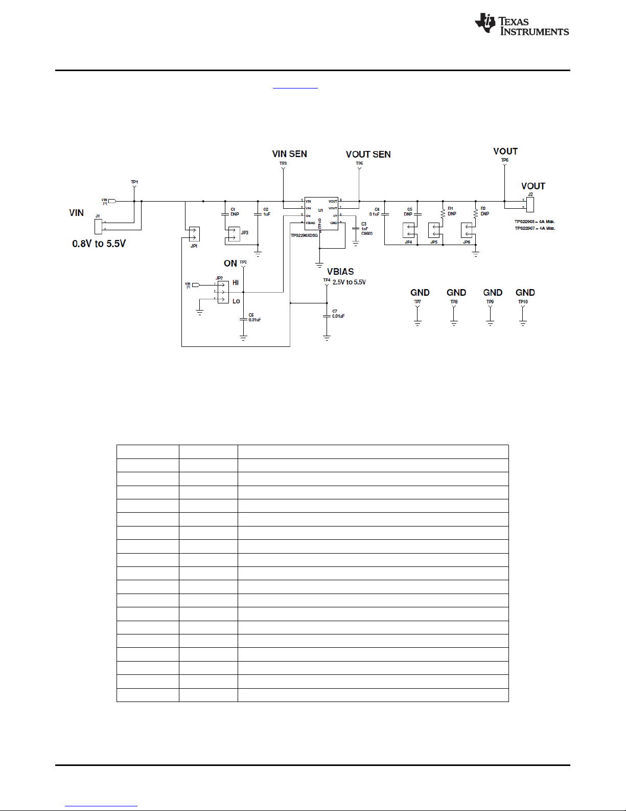
3 Schematic
www.ti.com
4 List of Test Points
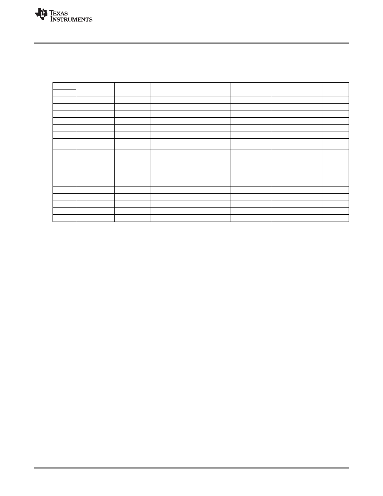
Test Points Name Description
J1 VIN DC Input to VIN
J2 VOUT VOUT Connection
JP1 VBIAS Connects VBIAS to VIN
JP2 ON Connects ON to VIN or GND
JP3 C1 Connects C1 to VIN
JP4 C5 Connects C5 to VOUT
JP5 R1 Connects R1 to VOUT
JP6 R2 Connects R2 to VOUT
TP1 VIN VIN of TPS22967
TP2 ON ON of TPS22967
TP3 VIN SEN Sense connect to VIN of TPS22967
TP4 VBIAS VBIAS of TPS22967
TP5 VOUT SEN Sense connect to VOUT of TPS22967
TP6 VOUT VOUT of TPS22967
TP7 GND Ground Connection
TP8 GND Ground Connection
TP9 GND Ground Connection
TP10 GND Ground Connection
Figure 1. TPS22967EVM-023 Schematic
Table 1. The Functions of Each Test Points
4
TPS22967EVM-023 Single 4A Load Switch SLVU951–August 2013
Copyright © 2013, Texas Instruments Incorporated
Submit Documentation Feedback
Page 5
www.ti.com
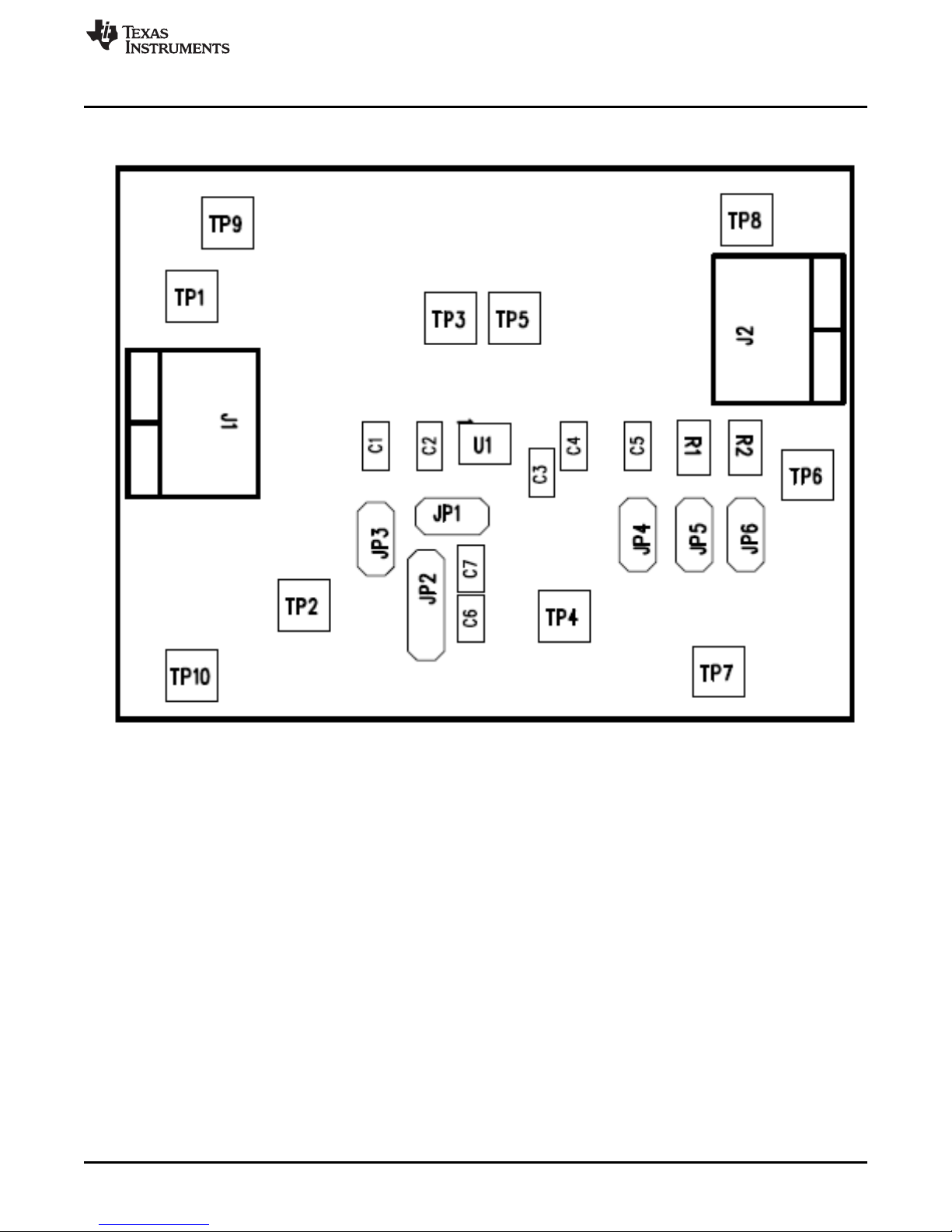
5 Layout
Layout
Figure 2. TPS22967EVM-023 Top Assembly
SLVU951–August 2013 TPS22967EVM-023 Single 4A Load Switch
Submit Documentation Feedback
5
Copyright © 2013, Texas Instruments Incorporated
Page 6

Layout
www.ti.com
6
TPS22967EVM-023 Single 4A Load Switch SLVU951–August 2013
Figure 3. TPS22967EVM-023 Topside
Copyright © 2013, Texas Instruments Incorporated
Submit Documentation Feedback
Page 7

www.ti.com
Layout
SLVU951–August 2013 TPS22967EVM-023 Single 4A Load Switch
Submit Documentation Feedback
Figure 4. TPS22967EVM-023 Bottomside
7
Copyright © 2013, Texas Instruments Incorporated
Page 8

Layout
5.1 Typical Test Setups
www.ti.com
Figure 5. TPS22967EVM-023 Recommended Ron Test Set Up
8
TPS22967EVM-023 Single 4A Load Switch SLVU951–August 2013
Copyright © 2013, Texas Instruments Incorporated
Submit Documentation Feedback
Page 9

www.ti.com
Layout
Figure 6. TPS22967EVM-023 Recommended Rise Time Test Set Up
5.2 Test Setup Equipment List
• Voltage Source:
– 1 Power Source capable of 10V 10A.
• Multimeters:
– 2 voltmeters
• Output Loads:
– Electronic Load or Resistor(If testing 4A operation of the switch at 5.5V a 22W power rated resistor
is needed)
• Oscilloscope:
– 2 channel 100MHz
• Signal Generator:
– Dual Channel Preferred
• Recommended Wire Gauge: 18 AWG
SLVU951–August 2013 TPS22967EVM-023 Single 4A Load Switch
Submit Documentation Feedback
9
Copyright © 2013, Texas Instruments Incorporated
Page 10

Performance Data and Typical Characteristic Curves
5.3 Test Procedure (Standalone Setup)
Figure 5 shows a typical setup for RONtesting of the EVM. VBIAS voltage must be present for the device
to function. Place a shunt across JP1 to connect VBIAS to VIN voltage source, if VIN supply is used below
2.5V remove the shunt and connect VBIAS voltage to a voltage source greater or equal to 2.5V.
5.4 RONTest Procedure
1. Setup the EVM per Figure 5.
2. Set SOURCE1 level to 5.0V.
3. Place a shunt on JP2 shorting pins 1 to 2. This connects ON to VIN voltage, ON voltage must be
between 1.2V and 5.5V for a valid ON state. (When testing RONit is desired to have the switch
operating in the always ON condition.)
4. Place a load on VOUT.
5. Turn on SOURCE1.
6. Record the voltage reading from Meter1, record the input current reading from Source1. Calculate R
by dividing Meter1 voltage level by the current reading from Source1. The results will be the RONvalue
for the Switch.
7. Turn off Source1.
5.5 Trise/Ton Tfall/Toff Test Procedure
1. Set up the EVM per Figure 6.
2. Set SOURCE1 level to 5.0V VBIAS is operational between 2.5V and 5.25V, Datasheet limits are
specified with VBIAS set at 5.0V.
3. Remove shunt from JP2.
4. Place a load on VOUT1 (a 10Ω 3.25W resistor is recommended for this test).
5. Set signal generator outputs to 0-2Vpp levels, 10–100Hz, and 25% duty cycle. Connect signal
generator output to TP2.
6. Turn on SOURCE1.
7. Turn ON the signal generator output.
8. Trise and Ton can be observed from the oscilloscope channel2. A detailed description of tR, tON, tF, and
t
are listed in the TPS22967 Datasheet under the Switching Characteristics Section.
OFF
9. Turn off Source1, and the signal generator output.
www.ti.com
ON
6 Performance Data and Typical Characteristic Curves
Figure 7 through Figure 8 present typical performance curves for TPS22967EVM-023.
10
TPS22967EVM-023 Single 4A Load Switch SLVU951–August 2013
Copyright © 2013, Texas Instruments Incorporated
Submit Documentation Feedback
Page 11

www.ti.com
6.1 Trise/Tfall Curves
Performance Data and Typical Characteristic Curves
Figure 7. TPS22967EVM-023 Trise/Ton VIN=5V VBIAS=5V ct=1nF Load =10Ω.
SLVU951–August 2013 TPS22967EVM-023 Single 4A Load Switch
Submit Documentation Feedback
11
Copyright © 2013, Texas Instruments Incorporated
Page 12

Performance Data and Typical Characteristic Curves
www.ti.com
Figure 8. TPS22967EVM-023 Tfall/Toff VIN=5V VBIAS=5V ct=1nF Load =10Ω.
12
TPS22967EVM-023 Single 4A Load Switch SLVU951–August 2013
Copyright © 2013, Texas Instruments Incorporated
Submit Documentation Feedback
Page 13
www.ti.com
7 Bill of Materials
Table 2 shows the EVM components list according to the schematic shown in Figure 1.
-002
Count
RefDes Value Description Size Part Number MFR
0 C1, C5 DNP Capacitor, Ceramic, 25V, X7R, 20% 0603 Std Std
1 C2 1 µF Capacitor, Ceramic, 25V, Y5R, 20% 0603 GRM188F51E105ZA12D Murata
1 C3 1 nf Capacitor, Ceramic, 50V, X7R, 10% 0603 ECJ-1VB1H102K Panasonic
1 C4 0.1 µF Capacitor, Ceramic, 50V, Y5R, 20% 0603 GRM188F51H104ZA01D Murata
2 C6, C7 0.01 µF Capacitor, Ceramic, 50V, X7R, 10% 0603 0603B103K500BT Vishay
2 J1, J2 ED120/2DS Terminal Block 2-pin, 15-A, 5.1mm 0.40 x 0.35 inch ED120/2DS OST
JP1, JP3, JP4, JP5,
5 PEC02SAAN Header, Male 2-pin, 100mil spacing 0.100 inch x 2 PEC02SAAN Sullins
JP6
1 JP2 PEC03SAAN Header,Male3-pin, 100mil spacing 0.100 inch x 3 PEC03SAAN Sullins
0 R1, R2 DNP Resistor, Chip, 1.16W, x% 0805 Std Std
TP1, TP2, TP3,
6 5010 Test Point, Red, Thru Hole Compact Style 0.125 x 0.125 inch 5005 Keystone
TP4, TP5, TP6
TP7, TP8, TP9,
4 5011 Test Point, Black, Thru Hole Compact Style 0.125 x 0.125 inch 5006 Keystone
TP10
0 U1 TPS22965DSG IC, 6-A Load Switch with Controlled Turn-on SON-8 TPS22965DSG TI
1 U1 TPS22967DSG IC, 4-A Load Switch with Controlled Turn-on SON-8 TPS22967DSG TI
2 Shunt, Black 100-mil 929950-00 3M
1 — PCB, 2 In x 1.5 In x 0.062 In HVL023 Any
1 NA Label (see Note 5) 1.25 x 0.25 inch THT-13-457-10 Brady
Bill of Materials
Table 2. EVM Components List
SLVU951–August 2013 TPS22967EVM-023 Single 4A Load Switch
Submit Documentation Feedback
13
Copyright © 2013, Texas Instruments Incorporated
Page 14

IMPORTANT NOTICE
Texas Instruments Incorporated and its subsidiaries (TI) reserve the right to make corrections, enhancements, improvements and other
changes to its semiconductor products and services per JESD46, latest issue, and to discontinue any product or service per JESD48, latest
issue. Buyers should obtain the latest relevant information before placing orders and should verify that such information is current and
complete. All semiconductor products (also referred to herein as “components”) are sold subject to TI’s terms and conditions of sale
supplied at the time of order acknowledgment.
TI warrants performance of its components to the specifications applicable at the time of sale, in accordance with the warranty in TI’s terms
and conditions of sale of semiconductor products. Testing and other quality control techniques are used to the extent TI deems necessary
to support this warranty. Except where mandated by applicable law, testing of all parameters of each component is not necessarily
performed.
TI assumes no liability for applications assistance or the design of Buyers’ products. Buyers are responsible for their products and
applications using TI components. To minimize the risks associated with Buyers’ products and applications, Buyers should provide
adequate design and operating safeguards.
TI does not warrant or represent that any license, either express or implied, is granted under any patent right, copyright, mask work right, or
other intellectual property right relating to any combination, machine, or process in which TI components or services are used. Information
published by TI regarding third-party products or services does not constitute a license to use such products or services or a warranty or
endorsement thereof. Use of such information may require a license from a third party under the patents or other intellectual property of the
third party, or a license from TI under the patents or other intellectual property of TI.
Reproduction of significant portions of TI information in TI data books or data sheets is permissible only if reproduction is without alteration
and is accompanied by all associated warranties, conditions, limitations, and notices. TI is not responsible or liable for such altered
documentation. Information of third parties may be subject to additional restrictions.
Resale of TI components or services with statements different from or beyond the parameters stated by TI for that component or service
voids all express and any implied warranties for the associated TI component or service and is an unfair and deceptive business practice.
TI is not responsible or liable for any such statements.
Buyer acknowledges and agrees that it is solely responsible for compliance with all legal, regulatory and safety-related requirements
concerning its products, and any use of TI components in its applications, notwithstanding any applications-related information or support
that may be provided by TI. Buyer represents and agrees that it has all the necessary expertise to create and implement safeguards which
anticipate dangerous consequences of failures, monitor failures and their consequences, lessen the likelihood of failures that might cause
harm and take appropriate remedial actions. Buyer will fully indemnify TI and its representatives against any damages arising out of the use
of any TI components in safety-critical applications.
In some cases, TI components may be promoted specifically to facilitate safety-related applications. With such components, TI’s goal is to
help enable customers to design and create their own end-product solutions that meet applicable functional safety standards and
requirements. Nonetheless, such components are subject to these terms.
No TI components are authorized for use in FDA Class III (or similar life-critical medical equipment) unless authorized officers of the parties
have executed a special agreement specifically governing such use.
Only those TI components which TI has specifically designated as military grade or “enhanced plastic” are designed and intended for use in
military/aerospace applications or environments. Buyer acknowledges and agrees that any military or aerospace use of TI components
which have not been so designated is solely at the Buyer's risk, and that Buyer is solely responsible for compliance with all legal and
regulatory requirements in connection with such use.
TI has specifically designated certain components as meeting ISO/TS16949 requirements, mainly for automotive use. In any case of use of
non-designated products, TI will not be responsible for any failure to meet ISO/TS16949.
Products Applications
Audio www.ti.com/audio Automotive and Transportation www.ti.com/automotive
Amplifiers amplifier.ti.com Communications and Telecom www.ti.com/communications
Data Converters dataconverter.ti.com Computers and Peripherals www.ti.com/computers
DLP® Products www.dlp.com Consumer Electronics www.ti.com/consumer-apps
DSP dsp.ti.com Energy and Lighting www.ti.com/energy
Clocks and Timers www.ti.com/clocks Industrial www.ti.com/industrial
Interface interface.ti.com Medical www.ti.com/medical
Logic logic.ti.com Security www.ti.com/security
Power Mgmt power.ti.com Space, Avionics and Defense www.ti.com/space-avionics-defense
Microcontrollers microcontroller.ti.com Video and Imaging www.ti.com/video
RFID www.ti-rfid.com
OMAP Applications Processors www.ti.com/omap TI E2E Community e2e.ti.com
Wireless Connectivity www.ti.com/wirelessconnectivity
Mailing Address: Texas Instruments, Post Office Box 655303, Dallas, Texas 75265
Copyright © 2013, Texas Instruments Incorporated
 Loading...