

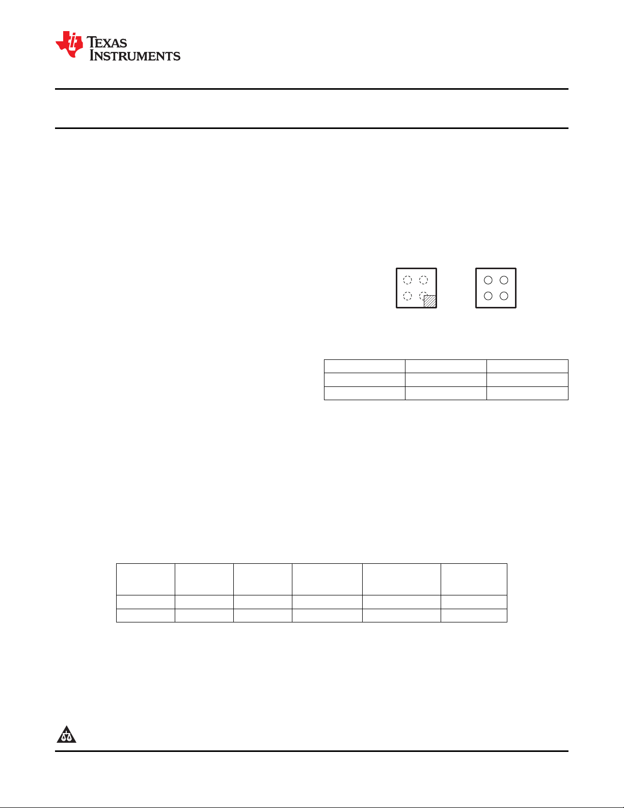
Bump View
1
2
B
A
Laser Marking View
2
1
B
A
www.ti.com
TPS22903
TPS22904
SLVS827C –FEBRUARY 2009–REVISED APRIL 2010
ULTRA-SMALL LOW-INPUT-VOLTAGE LOW rONLOAD SWITCH
Check for Samples: TPS22903, TPS22904
1
FEATURES
• Input Voltage: 1.1 V to 3.6 V
• Ultra-Low ON-State Resistance
– rON= 66 mΩ at VIN= 3.6 V
– rON= 75 mΩ at VIN= 2.5 V
– rON= 90 mΩ at VIN= 1.8 V
– rON= 135 mΩ at VIN= 1.2 V
• 500-mA Maximum Continuous Switch Current
• Quiescent Current < 1 mA
• Shutdown Current < 1 mA
• Low Control Input Threshold Enables Use of
1.2-V/1.8-V/2.5-V/3.3-V Logic
• Controlled Slew Rate (5 ms Max at 3.6 V)
• Quick Output Discharge (TPS22904 Only)
• ESD Performance Tested Per JESD 22
– 2000-V Human-Body Model
(A114-B, Class II)
– 1000-V Charged-Device Model (C101)
• 4-Terminal Wafer Chip-Scale Package (WCSP)
– 0.8 mm × 0.8 mm,
0.4-mm Pitch, 0.5-mm Height
APPLICATIONS
• PDAs
• Cell Phones
• GPS Devices
• MP3 Players
• Digital Cameras
• Peripheral Ports
• Portable Instrumentation
YFP PACKAGE
TERMINAL ASSIGNMENTS
B GND ON
A V
OUT
2 1
V
IN
DESCRIPTION
The TPS22903 and TPS22904 are ultra-small, low rONsingle channel load switches with controlled turn on. The
device contains a P-channel MOSFET that can operate over an input voltage range of 1.1 V to 3.6 V. The switch
is controlled by an on/off input (ON), which is capable of interfacing directly with low-voltage control signals. In
TPS22904, a 85-Ω on-chip load resistor is added for output quick discharge when switch is turned off.
TPS22903 and TPS22904 are available in a space-saving 4-terminal WCSP 0.4-mm pitch (YFP). The devices
are characterized for operation over the free-air temperature range of –40°C to 85°C.
1
PRODUCTION DATA information is current as of publication date.
Products conform to specifications per the terms of the Texas
Instruments standard warranty. Production processing does not
necessarily include testing of all parameters.
FEATURE LIST
DEVICE OUTPUT ENABLE
TPS22903 66 mΩ 5 ms max No 500 mA Active high
TPS22904 66 mΩ 5 ms max Yes 500 mA Active high
(1) This feature discharges the output of the switch to ground through a 85-Ω resistor, preventing the
output from floating.
Please be aware that an important notice concerning availability, standard warranty, and use in critical applications of Texas
Instruments semiconductor products and disclaimers thereto appears at the end of this data sheet.
rONTYPICAL SLEW RATE QUICK OUTPUT
AT 3.6 V AT 3.6 V DISCHARGE
(1)
MAXIMUM
CURRENT
Copyright © 2009–2010, Texas Instruments Incorporated
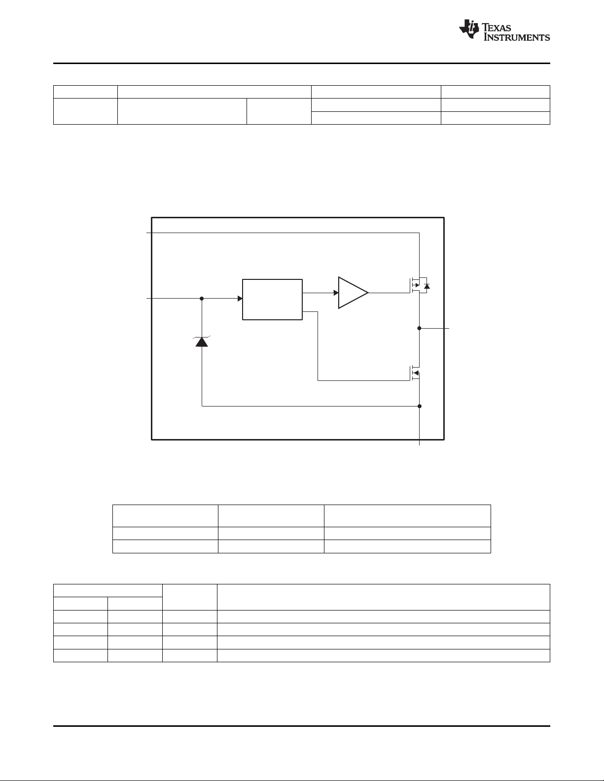
ON
V
OUT
GND
Turn-On Slew Rate
Controlled Driver
ESD Protection
V
IN
Control
Logic
A1
B1
A2
B2
Output Discharge
TPS22904 Only
TPS22903
TPS22904
SLVS827C –FEBRUARY 2009–REVISED APRIL 2010
ORDERING INFORMATION
T
A
–40°C to 85°C WCSP – YFP (0.4-mm pitch) Tape and reel
(1) For the most current package and ordering information, see the Package Option Addendum at the end of this document, or see the TI
web site at www.ti.com.
(2) Package drawings, thermal data, and symbolization are available at www.ti.com/packaging.
(3) The actual top-side marking has three preceding characters to denote year, month, and sequence code, and one following character to
designate the wafer fab/assembly site. Pin 1 identifier indicates solder-bump composition (1 = SnPb, • = Pb-free).
PACKAGE
(2)
ORDERABLE PART NUMBER TOP-SIDE MARKING
TPS22903YFPR _ _ _4P_
TPS22904YFPR _ _ _4R_
(1)
BLOCK DIAGRAM
www.ti.com
(3)
Figure 1. Functional Block Diagram
FUNCTION TABLE
IN
OUT
ON
L OFF ON
H ON OFF
I/O DESCRIPTION
I Input of the switch, bypass this input with a ceramic capacitor to ground
O Output of the switch
(CONTROL INPUT)
TERMINAL
BALL NO. NAME
A1 V
A2 V
B1 ON I Switch control input, active high, do not leave floating
B2 GND – Ground
2 Submit Documentation Feedback Copyright © 2009–2010, Texas Instruments Incorporated
VINTO V
OUT
V
TO GND (TPS22904 ONLY)
OUT
TERMINAL FUNCTIONS
Product Folder Link(s): TPS22903 TPS22904
www.ti.com
TPS22903
TPS22904
SLVS827C –FEBRUARY 2009–REVISED APRIL 2010
ABSOLUTE MAXIMUM RATINGS
(1)
MIN MAX UNIT
V
IN
V
OUT
V
ON
P
D
I
MAX
T
A
T
stg
T
lead
ESD Electrostatic discharge protection V
Input voltage range –0.3 4 V
Output voltage range VIN+ 0.3 V
Input voltage range –0.3 4 V
Power dissipation at TA= 25°C 0.48 W
Maximum continuous switch current 0.5 A
Operating free-air temperature range –40 85 °C
Storage temperature range –65 150 °C
Maximum lead temperature (10-s soldering time) 300 °C
Human-Body Model (HBM) 2000
Charged Device Model (CDM) 1000
(1) Stresses beyond those listed under absolute maximum ratings may cause permanent damage to the device. These are stress ratings
only, and functional operation of the device at these or any other conditions beyond those indicated under Recommended Operating
Conditions is not implied. Exposure to absolute-maximum-rated conditions for extended periods may affect device reliability.
THERMAL IMPEDANCE RATINGS
TYP UNIT
q
Package thermal impedance
JA
(1)
YFP package 205 °C/W
(1) The package thermal impedance is calculated in accordance with JESD 51-7.
RECOMMENDED OPERATING CONDITIONS
MIN MAX UNIT
V
V
V
V
C
(1) See Application Information
Input voltage range 1.1 3.6 V
IN
Output voltage range V
OUT
High-level input voltage, ON 0.85 3.6 V
IH
Low-level input voltage, ON 0.4 V
IL
IN
Input capacitor
(1)
IN
1 mF
V
Copyright © 2009–2010, Texas Instruments Incorporated Submit Documentation Feedback 3
Product Folder Link(s): TPS22903 TPS22904
TPS22903
TPS22904
SLVS827C –FEBRUARY 2009–REVISED APRIL 2010
ELECTRICAL CHARACTERISTICS
VIN= 1.1 V to 3.6 V, TA= –40°C to 85°C (unless otherwise noted)
PARAMETER TEST CONDITIONS T
I
IN
I
IN(OFF)
I
IN(LEAKAGE)
r
ON
r
PD
I
ON
(1) Typical values are at VIN= 3.3 V and TA= 25°C.
Quiescent current I
= 0, VIN= V
OUT
ON
OFF-state supply current VON= GND, OUT = Open Full 1 mA
OFF-state switch current VON= GND, V
ON-state resistance I
Output pulldown resistance 85 135 Ω
= –200 mA VIN= 1.8 V mΩ
OUT
VIN= 3.3 V, VON= 0 (TPS22904 only),
I
= 30 mA
OUT
OUT
ON-state input leakage current VON= 1.1 V to 3.6 V or GND Full 1 mA
www.ti.com
A
MIN TYP
(1)
MAX UNIT
Full 1 mA
= 0 Full 1 mA
VIN= 3.6 V
VIN= 2.5 V
25°C 66 90
Full 95
25°C 75 95
Full 110
25°C 90 115
Full 125
VIN= 1.2 V
VIN= 1.1 V
25°C 135 175
Full 185
25°C 157 275
Full 300
SWITCHING CHARACTERISTICS
VIN= 3.6 V, TA= –40°C to 85°C (unless otherwise noted)
PARAMETER TEST CONDITIONS
t
ON
t
OFF
t
r
t
f
(1) Typical values are at TA= 25°C.
Turn-ON time I
Turn-OFF time I
V
rise time I
OUT
V
fall time I
OUT
= 100 mA, CL= 0.1 mF 0.9 1.5 0.9 1.5 ms
OUT
= 100 mA, CL= 0.1 mF 5.8 8 5.3 7 ms
OUT
= 100 mA, CL= 0.1 mF 0.80 5 0.8 5 ms
OUT
= 100 mA, CL= 0.1 mF 8.3 10 5.8 7 ms
OUT
TPS22903 TPS22904
MIN TYP
(1)
MAX MIN TYP
(1)
MAX UNIT
4 Submit Documentation Feedback Copyright © 2009–2010, Texas Instruments Incorporated
Product Folder Link(s): TPS22903 TPS22904
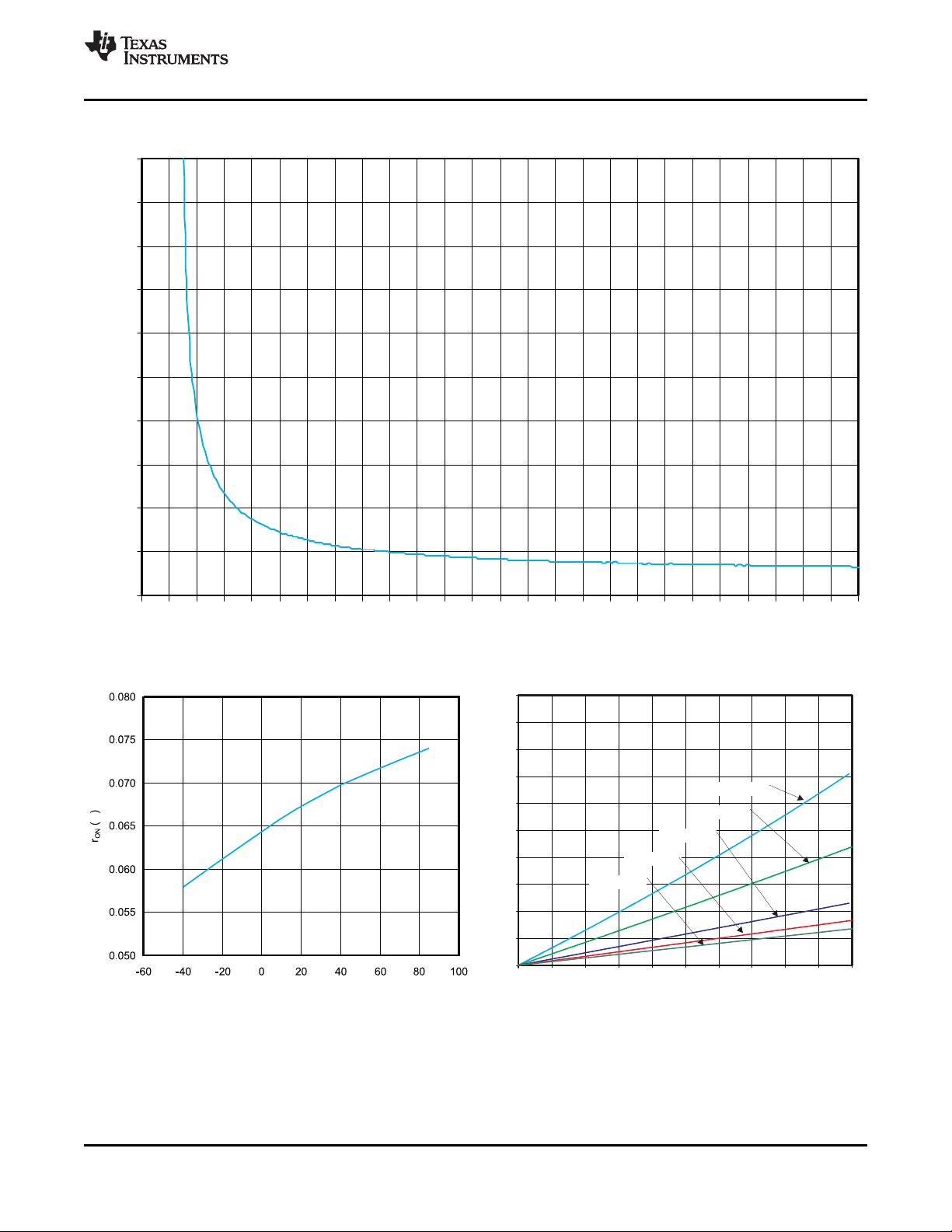
Input Voltage, (V)V
IN
ON-State Resistance, ( )r
ON
Ω
0.0
0.1
0.2
0.3
0.4
0.5
0.6
0.7
0.8
0.9
1.0
0.7 0.8 0.9 1.0 1.1 1.2 1.3 1.4 1.5 1.6 1.7 1.8 1.9 2.0 2.1 2.2 2.3 2.4 2.5 2.6 2.7 2.8 2.9 3.0 3.1 3.2 3.3
0.00 0.05 0.10 0.15 0.20 0.25 0.30 0.35 0.40 0.45 0.50
Load Current (A)
0
10
20
30
40
50
60
70
80
90
100
Voltage Drop (mV)
V = 1.0 V
drop
V = 1.2 V
drop
V = 1.8 V
drop
V = 2.5 V
drop
V = 3.3 V
drop
W
Temperature(°C)
www.ti.com
TPS22903
TPS22904
SLVS827C –FEBRUARY 2009–REVISED APRIL 2010
TYPICAL CHARACTERISTICS
Figure 2. rONvs V
IN
Copyright © 2009–2010, Texas Instruments Incorporated Submit Documentation Feedback 5
Figure 3. rONvs Temperature (VIN= 3.3 V) Figure 4. Voltage Drop vs Load Current
Product Folder Link(s): TPS22903 TPS22904

–40 25 85
Temperature(°C)
0
50
100
150
200
250
Quiescent Current, I (nA)
IN
Input Voltage, V (V)
IN
Quiescent Current, I (nA)
IN
0
20
40
60
80
100
120
140
160
180
200
0.5 1.0 1.5 2.0 2.5 3.0 3.5 4.0
–40 25 85
Temperature(°C)
I Current (nA)
IN(OFF)
25
50
75
100
125
150
175
200
225
250
0
Input Voltage, V (V)
IN
0
20
40
60
80
100
120
0.5 1.0 1.5 2.0 2.5 3.0 3.5 4.0
I Current (nA)
IN(OFF)
TPS22903
TPS22904
SLVS827C –FEBRUARY 2009–REVISED APRIL 2010
TYPICAL CHARACTERISTICS (continued)
www.ti.com
Figure 5. Quiescent Current vs V
(VON= VIN, I
Figure 7. I
IN(OFF)
= 0) (VIN= 3.3 V, I
OUT
vs VIN(VON= 0 V) Figure 8. I
IN
Figure 6. Quiescent Current vs Temperature
= 0)
OUT
vs Temperature (VIN= 3.3 V)
IN(OFF)
6 Submit Documentation Feedback Copyright © 2009–2010, Texas Instruments Incorporated
Product Folder Link(s): TPS22903 TPS22904

I (Leakage) Current (nA)
IN
0
25
50
75
100
125
150
175
200
225
250
–40 25 85
Temperature (°C)
Input Voltage, (V)V
IN
1.5 2.0 2.5 3.0 3.5 4.01.00.5
20
40
60
80
100
120
0
I (Leakage) Current (nA)
IN
–0.5
0.0
0.5
1.0
1.5
2.0
2.5
3.0
3.5
4.0
0.3 0.4 0.5 0.6 0.7 0.8
V (V)
OUT
Input Voltage, V (V)
ON
VIN= 3.6 V
VIN= 1.1 V
VIN= 1.2 V
VIN= 1.5 V
VIN= 1.8 V
VIN= 2.5 V
VIN= 3 V
VIN= 3.3 V
www.ti.com
TPS22903
TPS22904
SLVS827C –FEBRUARY 2009–REVISED APRIL 2010
TYPICAL CHARACTERISTICS (continued)
Figure 9. IIN(Leakage) vs VIN(I
= 0) Figure 10. IIN(Leakage) vs Temperature (VIN= 3.3 V)
OUT
Figure 11. ON-Input Threshold
Copyright © 2009–2010, Texas Instruments Incorporated Submit Documentation Feedback 7
Product Folder Link(s): TPS22903 TPS22904

t /t ( s)
Irise fall
m
0
7
Temperature (°C)
1
2
3
4
5
6
–40 –20 0 20 40 60 80 100
t
fall
C = 0.1 µF
I = 100 mA
L
L
t
rise
t /t ( s)
ON OFF
m
0.0
6.0
Temperature (°C)
–40 –20 0 20 40 60 80 100
0.5
1.0
1.5
2.0
2.5
3.0
3.5
4.0
4.5
5.0
5.5
C = 0.1 µF
I = 100 mA
L
L
t
ON
t
OFF
0
1
2
3
4
5
6
-40 -20 0 20 40 60 80 100
Temperature (°C)
t
fall
(µs)
CL= 0.1 µF
IL= 100 mA
t
fall
4
4.5
5
5.5
6
-40 -20 0 20 40 60 80 100
Temperature (°C)
t
OFF
(µs)
CL= 0.1 µF
IL= 100 mA
t
OFF
TPS22903
TPS22904
SLVS827C –FEBRUARY 2009–REVISED APRIL 2010
TYPICAL CHARACTERISTICS (continued)
www.ti.com
Figure 12. t
Figure 14. t
(TPS22903/4) / t
rise
fall
(VIN= 3.3 V) (VIN= 3.3 V)
(TPS22904) vs Temperature (VIN= 3.3 V) Figure 15. t
(TPS22903) vs Temperature Figure 13. tON(TPS22903/4) / t
fall
(TPS22903) vs Temperature
OFF
(TPS22904) vs Temperature (VIN= 3.3 V)
OFF
8 Submit Documentation Feedback Copyright © 2009–2010, Texas Instruments Incorporated
Product Folder Link(s): TPS22903 TPS22904

I
20 mA/DIV
OUT
V
200 mV/DIV
ON
5 s/DIVm
C = 0.1 F
I = 100 mA
V = 1.2 V
L
OUT
IN
m
I
20 mA/DIV
OUT
V
200 mV/DIV
ON
20 s/DIVm
C = 10 F
I = 100 mA
V = 1.2 V
L
OUT
IN
m
I
20 mA/DIV
OUT
V
200 mV/DIV
ON
5 s/DIVm
C = 0.1 F
I = 100 mA
V = 3.3 V
L
OUT
IN
m
I
20 mA/DIV
OUT
V
200 mV/DIV
ON
20 s/DIVm
C = 10 F
I = 100 mA
V = 3.3 V
L
OUT
IN
m
www.ti.com
TPS22903
TPS22904
SLVS827C –FEBRUARY 2009–REVISED APRIL 2010
TYPICAL CHARACTERISTICS (continued)
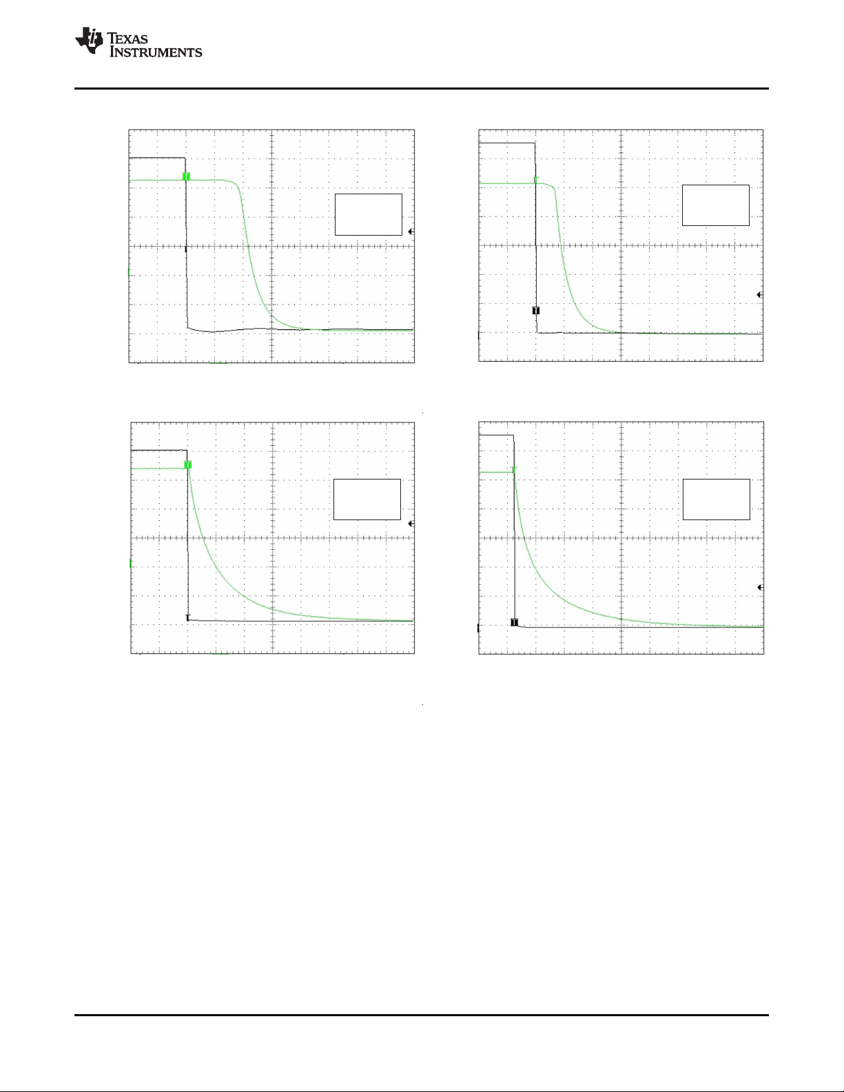
Figure 16. tONResponse Figure 17. tONResponse
Figure 18. tONResponse Figure 19. tONResponse
Copyright © 2009–2010, Texas Instruments Incorporated Submit Documentation Feedback 9
Product Folder Link(s): TPS22903 TPS22904

I
20 mA/DIV
OUT
V
200 mV/DIV
ON
2 s/DIVm
C = 0.1 F
I = 100 mA
V = 1.2 V
L
OUT
IN
m
I
20 mA/DIV
OUT
V
200 mV/DIV
ON
100 s/DIVm
C = 10 F
I = 100 mA
V = 1.2 V
L
OUT
IN
m
I
20 mA/DIV
OUT
V
200 mV/DIV
ON
5 s/DIVm
C = 0.1 F
I = 100 mA
V = 3.3 V
L
OUT
IN
m
I
20 mA/DIV
OUT
V
200 mV/DIV
ON
200 s/DIVm
C = 10 F
I = 100 mA
V = 3.3 V
L
OUT
IN
m
TPS22903
TPS22904
SLVS827C –FEBRUARY 2009–REVISED APRIL 2010
TYPICAL CHARACTERISTICS (continued)
www.ti.com
Figure 20. t
Figure 22. t
Response (TPS22903) Figure 21. t
OFF
Response (TPS22903) Figure 23. t
OFF
Response (TPS22903)
OFF
Response (TPS22903)
OFF
10 Submit Documentation Feedback Copyright © 2009–2010, Texas Instruments Incorporated
Product Folder Link(s): TPS22903 TPS22904
I
20 mA/DIV
OUT
V
200 mV/DIV
ON
5 s/DIVm
C = 0.1 F
I = 100 mA
V = 3.3 V
L
OUT
IN
m
I
20 mA/DIV
OUT
V
200 mV/DIV
ON
2 s/DIVm
C = 0.1 F
I = 100 mA
V = 1.2 V
L
OUT
IN
m
I
20 mA/DIV
OUT
V
200 mV/DIV
ON
100 s/DIVm
C = 10 F
I = 100 mA
V = 1.2 V
L
OUT
IN
m
I
20 mA/DIV
OUT
V
200 mV/DIV
ON
200 s/DIVm
C = 10 F
I = 100 mA
V = 3.3 V
L
OUT
IN
m
www.ti.com
TPS22903
TPS22904
SLVS827C –FEBRUARY 2009–REVISED APRIL 2010
TYPICAL CHARACTERISTICS (continued)
Figure 24. t
Figure 26. t
Response (TPS22904) Figure 25. t
OFF
Response (TPS22904) Figure 27. t
OFF
Response (TPS22904)
OFF
Response (TPS22904)
OFF
Copyright © 2009–2010, Texas Instruments Incorporated Submit Documentation Feedback 11
Product Folder Link(s): TPS22903 TPS22904

ON
(A)
OFF
TPS22903
GND
GND
GND
R
L
C
L
V
OUT
V
IN
CIN=10 x C
L
+
–
90% 90%
V
OUT
t
r
t
f
10%10%
V /2
OUT
V
OUT
V /2
OUT
V /2
ON
V /2
ON
V
ON
V
ON
0 V
0 V
1.8 V
V
OH
V
OL
t
ON
t
OFF
TEST CIRCUIT
t /t WAVEFORMS
ON OFF
TPS22903
TPS22904
SLVS827C –FEBRUARY 2009–REVISED APRIL 2010
PARAMETER MEASUREMENT INFORMATION
www.ti.com
A. t
and t
rise
of the control signal is 100 ns.
fall
Figure 28. Test Circuit and tON/t
Waveforms
OFF
12 Submit Documentation Feedback Copyright © 2009–2010, Texas Instruments Incorporated
Product Folder Link(s): TPS22903 TPS22904

TPS22903
TPS22904
www.ti.com
APPLICATION INFORMATION
ON/OFF Control
The ON pin controls the state of the switch. Activating ON continuously holds the switch in the on state as there
is no fault. ON is active-high and has a low threshold, making it capable of interfacing with low-voltage signals.
The ON pin is compatible with standard GPIO logic thresholds. It can be used with any microcontroller with
1.2-V, 1.8-V, 2.5-V, or 3.3-V GPIOs.
Input Capacitor
To limit the voltage drop on the input supply caused by transient in-rush currents when the switch turns on into a
discharged load capacitor or short-circuit, a capacitor needs to be placed between VINand GND. A 1-mF ceramic
capacitor, CIN, placed close to the pins, is usually sufficient. Higher values of CINcan be used to further reduce
the voltage drop during high-current application. When switching heavy loads, it is recommended to have an
input capacitor about 10 times higher than the output capacitor to avoid excessive voltage drop.
Output Capacitor
Due to the integral body diode in the PMOS switch, a CINgreater than CLis highly recommended. A CLgreater
than CINcan cause V
through the body diode from V
to exceed VINwhen the system supply is removed. This could result in current flow
OUT
OUT
to VIN.
Board Layout
For best performance, all traces should be as short as possible. To be most effective, the input and output
capacitors should be placed close to the device to minimize the effects that parasitic trace inductances may have
on normal and short-circuit operation. Using wide traces for VIN, V
electrical effects along with minimizing the case-to-ambient thermal impedance.
SLVS827C –FEBRUARY 2009–REVISED APRIL 2010
, and GND helps minimize the parasitic
OUT
Copyright © 2009–2010, Texas Instruments Incorporated Submit Documentation Feedback 13
Product Folder Link(s): TPS22903 TPS22904

PACKAGE OPTION ADDENDUM
www.ti.com 24-Apr-2010
PACKAGING INFORMATION
Orderable Device Status
(1)
Package
Type
Package
Drawing
Pins Package
Qty
Eco Plan
TPS22903YFPR ACTIVE DSBGA YFP 4 3000 Green (RoHS &
(2)
Lead/Ball Finish MSL Peak Temp
SNAGCU Level-1-260C-UNLIM
(3)
no Sb/Br)
TPS22904YFPR ACTIVE DSBGA YFP 4 3000 Green (RoHS &
SNAGCU Level-1-260C-UNLIM
no Sb/Br)
TPS22904YFPT ACTIVE DSBGA YFP 4 250 Green (RoHS &
Call TI Level-1-260C-UNLIM
no Sb/Br)
(1)
The marketing status values are defined as follows:
ACTIVE: Product device recommended for new designs.
LIFEBUY: TI has announced that the device will be discontinued, and a lifetime-buy period is in effect.
NRND: Not recommended for new designs. Device is in production to support existing customers, but TI does not recommend using this part in
a new design.
PREVIEW: Device has been announced but is not in production. Samples may or may not be available.
OBSOLETE: TI has discontinued the production of the device.
(2)
Eco Plan - The planned eco-friendly classification: Pb-Free (RoHS), Pb-Free (RoHS Exempt), or Green (RoHS & no Sb/Br) - please check
http://www.ti.com/productcontent for the latest availability information and additional product content details.
TBD: The Pb-Free/Green conversion plan has not been defined.
Pb-Free (RoHS): TI's terms "Lead-Free" or "Pb-Free" mean semiconductor products that are compatible with the current RoHS requirements
for all 6 substances, including the requirement that lead not exceed 0.1% by weight in homogeneous materials. Where designed to be soldered
at high temperatures, TI Pb-Free products are suitable for use in specified lead-free processes.
Pb-Free (RoHS Exempt): This component has a RoHS exemption for either 1) lead-based flip-chip solder bumps used between the die and
package, or 2) lead-based die adhesive used between the die and leadframe. The component is otherwise considered Pb-Free (RoHS
compatible) as defined above.
Green (RoHS & no Sb/Br): TI defines "Green" to mean Pb-Free (RoHS compatible), and free of Bromine (Br) and Antimony (Sb) based flame
retardants (Br or Sb do not exceed 0.1% by weight in homogeneous material)
(3)
MSL, Peak Temp. -- The Moisture Sensitivity Level rating according to the JEDEC industry standard classifications, and peak solder
temperature.
Important Information and Disclaimer:The information provided on this page represents TI's knowledge and belief as of the date that it is
provided. TI bases its knowledge and belief on information provided by third parties, and makes no representation or warranty as to the
accuracy of such information. Efforts are underway to better integrate information from third parties. TI has taken and continues to take
reasonable steps to provide representative and accurate information but may not have conducted destructive testing or chemical analysis on
incoming materials and chemicals. TI and TI suppliers consider certain information to be proprietary, and thus CAS numbers and other limited
information may not be available for release.
In no event shall TI's liability arising out of such information exceed the total purchase price of the TI part(s) at issue in this document sold by TI
to Customer on an annual basis.
Addendum-Page 1


IMPORTANT NOTICE
Texas Instruments Incorporated and its subsidiaries (TI) reserve the right to make corrections, modifications, enhancements, improvements,
and other changes to its products and services at any time and to discontinue any product or service without notice. Customers should
obtain the latest relevant information before placing orders and should verify that such information is current and complete. All products are
sold subject to TI’s terms and conditions of sale supplied at the time of order acknowledgment.
TI warrants performance of its hardware products to the specifications applicable at the time of sale in accordance with TI’s standard
warranty. Testing and other quality control techniques are used to the extent TI deems necessary to support this warranty. Except where
mandated by government requirements, testing of all parameters of each product is not necessarily performed.
TI assumes no liability for applications assistance or customer product design. Customers are responsible for their products and
applications using TI components. To minimize the risks associated with customer products and applications, customers should provide
adequate design and operating safeguards.
TI does not warrant or represent that any license, either express or implied, is granted under any TI patent right, copyright, mask work right,
or other TI intellectual property right relating to any combination, machine, or process in which TI products or services are used. Information
published by TI regarding third-party products or services does not constitute a license from TI to use such products or services or a
warranty or endorsement thereof. Use of such information may require a license from a third party under the patents or other intellectual
property of the third party, or a license from TI under the patents or other intellectual property of TI.
Reproduction of TI information in TI data books or data sheets is permissible only if reproduction is without alteration and is accompanied
by all associated warranties, conditions, limitations, and notices. Reproduction of this information with alteration is an unfair and deceptive
business practice. TI is not responsible or liable for such altered documentation. Information of third parties may be subject to additional
restrictions.
Resale of TI products or services with statements different from or beyond the parameters stated by TI for that product or service voids all
express and any implied warranties for the associated TI product or service and is an unfair and deceptive business practice. TI is not
responsible or liable for any such statements.
TI products are not authorized for use in safety-critical applications (such as life support) where a failure of the TI product would reasonably
be expected to cause severe personal injury or death, unless officers of the parties have executed an agreement specifically governing
such use. Buyers represent that they have all necessary expertise in the safety and regulatory ramifications of their applications, and
acknowledge and agree that they are solely responsible for all legal, regulatory and safety-related requirements concerning their products
and any use of TI products in such safety-critical applications, notwithstanding any applications-related information or support that may be
provided by TI. Further, Buyers must fully indemnify TI and its representatives against any damages arising out of the use of TI products in
such safety-critical applications.
TI products are neither designed nor intended for use in military/aerospace applications or environments unless the TI products are
specifically designated by TI as military-grade or "enhanced plastic." Only products designated by TI as military-grade meet military
specifications. Buyers acknowledge and agree that any such use of TI products which TI has not designated as military-grade is solely at
the Buyer's risk, and that they are solely responsible for compliance with all legal and regulatory requirements in connection with such use.
TI products are neither designed nor intended for use in automotive applications or environments unless the specific TI products are
designated by TI as compliant with ISO/TS 16949 requirements. Buyers acknowledge and agree that, if they use any non-designated
products in automotive applications, TI will not be responsible for any failure to meet such requirements.
Following are URLs where you can obtain information on other Texas Instruments products and application solutions:
Products Applications
Amplifiers amplifier.ti.com Audio www.ti.com/audio
Data Converters dataconverter.ti.com Automotive www.ti.com/automotive
DLP® Products www.dlp.com Communications and www.ti.com/communications
DSP dsp.ti.com Computers and www.ti.com/computers
Clocks and Timers www.ti.com/clocks Consumer Electronics www.ti.com/consumer-apps
Interface interface.ti.com Energy www.ti.com/energy
Logic logic.ti.com Industrial www.ti.com/industrial
Power Mgmt power.ti.com Medical www.ti.com/medical
Microcontrollers microcontroller.ti.com Security www.ti.com/security
RFID www.ti-rfid.com Space, Avionics & www.ti.com/space-avionics-defense
RF/IF and ZigBee® Solutions www.ti.com/lprf Video and Imaging www.ti.com/video
Mailing Address: Texas Instruments, Post Office Box 655303, Dallas, Texas 75265
Copyright © 2010, Texas Instruments Incorporated
Telecom
Peripherals
Defense
Wireless www.ti.com/wireless-apps
 Loading...