

Datasheet TPS2231MRGPR, TPS2231MRGPR-2, TPS2231MRGPR-3, TPS2231PW, TPS2231PWP Datasheet (Texas Instruments) [ru]
...
RGP PW PWP DAP
AUXIN
3.3VIN
1.5VIN
AUXOUT
3.3VOUT
1.5VOUT
PERST
CPPE
CPUSB
SHDN
STBY
SYSRST
OC
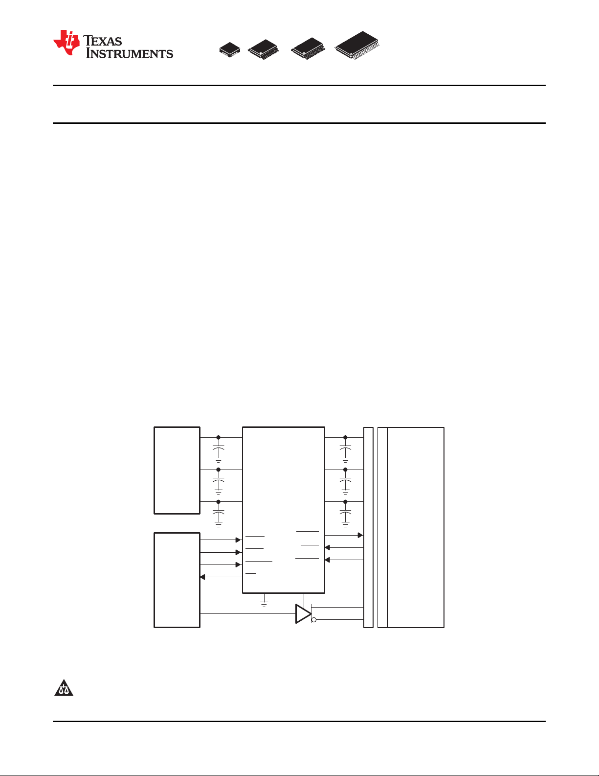
TPS2231
Host Connector
ExpressCard Connector
GND RCLKEN
REFCLK+
REFCLK−
Express Card
Host
Power
Source
Host
Chip
Set/Lock
Circuits
www.ti.com
TPS2231
TPS2236
.................................................................................................................................................. SLVS536J –JULY 2004–REVISED SEPTEMBER 2009
ExpressCard™ POWER INTERFACE SWITCH
Check for Samples: TPS2231 TPS2236
1
FEATURES
23
• Meets the ExpressCard™ Standard
• Available in a 20-pin TSSOP, a 20-pin QFN, or
24-pin PowerPAD™ HTSSOP (Single)
(ExpressCard|34 or ExpressCard|54) • Available in a 32-pin PowerPAD™ HTSSOP
• Compliant with the ExpressCard™
(Dual)
Compliance Checklists
• Fully Satisfies the ExpressCard™
Implementation Guidelines
• Supports Systems with WAKE Function
• TTL-Logic Compatible Inputs
• Short Circuit and Thermal Protection
• –40°C to 85°C Ambient Operating
APPLICATIONS
• Notebook Computers
• Desktop Computers
• Personal Digital Assistants (PDAs)
• Digital Cameras
• TV and Set Top Boxes
Temperature Range
DESCRIPTION
The TPS2231 and TPS2236 ExpressCard power interface switches provide the total power management solution
required by the ExpressCard specification. The TPS2231 and TPS2236 ExpressCard power interface switches
distribute 3.3 V, AUX, and 1.5 V to the ExpressCard socket. Each voltage rail is protected with integrated
current-limiting circuitry.
The TPS2231 supports systems with single-slot ExpressCard|34 or ExpressCard|54 sockets. The TPS2236
supports systems with dual-slot ExpressCard sockets.
End equipment for the TPS2231 and TPS2236 include notebook computers, desktop computers, personal digital
assistants (PDAs), and digital cameras.
1
2PowerPAD is a trademark of Texas Instruments.
3ExpressCard is a trademark of Personal Computer Memory Card International Association.
PRODUCTION DATA information is current as of publication date.
Products conform to specifications per the terms of the Texas
Instruments standard warranty. Production processing does not
necessarily include testing of all parameters.
Please be aware that an important notice concerning availability, standard warranty, and use in critical applications of Texas
Instruments semiconductor products and disclaimers thereto appears at the end of this data sheet.
Copyright © 2004–2009, Texas Instruments Incorporated
TPS2231
TPS2236
SLVS536J –JULY 2004–REVISED SEPTEMBER 2009..................................................................................................................................................
This integrated circuit can be damaged by ESD. Texas Instruments recommends that all integrated circuits be handled with
appropriate precautions. Failure to observe proper handling and installation procedures can cause damage.
ESD damage can range from subtle performance degradation to complete device failure. Precision integrated circuits may be more
susceptible to damage because very small parametric changes could cause the device not to meet its published specifications.
www.ti.com
AVAILABLE OPTIONS
T
A
NUMBER OF CHANNELS
TSSOP PowerPAD HTSSOP QFN
PACKAGED DEVICES
–40°C to 85°C Single TPS2231PW TPS2231PWP TPS2231MRGP-1
Dual TPS2236DAP
(1) The package is available taped and reeled. Add an R suffix to device types (e.g., TPS2231PWPR).
(2) For the most current package and ordering information, see the Package Option Addendum at the end of this document, or see the TI
website at www.ti.com.
(3) The TPS2231MRGP is identical to the TPS2231 with the exception of the PowerPAD dimensions. See the Thermal Pad Mechanical
data portion of this data sheet for specific information. The thermal pad for the TPS2231MRGP and TPS2231MRGP-1 is 2,2 mm × 2,2
mm; the thermal pad for the TPS2231RGP is 2,7 mm × 2,7 mm.
(4) The TPS2231MRGP-1 is identical to the TPS2231MGRP with the exception that the orientation of the part in the reel is rotated 180°.
See the Package Materials Information portion of this data sheet for specific information.
(5) The TPS2231MRGP-2 is identical to the TPS2231MRGP with the exception that the orientation of the part in the reel is rotated 90° and
does not have an internal pull-up resistor between AUX IN and SYSRST. See the Package Materials Information portion of this data
sheet for specific information.
(6) The TPS2231MRGP-3 is identical to the TPS2231MRGP with the exception that the 1.5VIN and 3.3VIN UVLO circuits are independent.
(1) (2)
TPS2231RGP
TPS2231MRGP
TPS2231MRGP-2
TPS2231MRGP-3
(3)
(4)
(5)
(6)
ABSOLUTE MAXIMUM RATINGS
over operating free-air temperature range (unless otherwise noted)
V
V
I
Input voltage range for card
power
Logic input/output voltage –0.3 to 6 V
V
O
Output voltage range V
Continuous total power dissipation See Dissipation Rating Table
I
O
Output current I
OC sink current 10 mA
PERST sink/source current 10 mA
T
J
T
stg
Operating virtual junction temperature range –40 to 120 °C
Storage temperature range –55 to 150 °C
Lead temperature 1,6 mm (1/16 inch) from case for 10 seconds 260 °C
ESD
Electrostatic discharge
protection
(1) Stresses beyond those listed under absolute maximum ratings may cause permanent damage to the device. These are stress ratings
only, and functional operation of the device at these or any other conditions beyond those indicated under recommended operating
conditions is not implied. Exposure to absolute-maximum-rated conditions for extended periods may affect device reliability.
I(3.3VIN)
V
I(1.5VIN)
V
I(AUXIN)
V
O(3.3VOUT)
O(1.5VOUT)
V
O(AUXOUT)
I
O(3.3VOUT)
O(AUXOUT)
I
O(1.5VOUT)
Human body model TPS2236, all pins except
(HBM) MIL-STD-883C PERSTx and OCx
Charge device model (CDM) 500 V
(1)
TPS223x UNIT
–0.3 to 6 V
–0.3 to 6 V
–0.3 to 6 V
–0.3 to 6 V
–0.3 to 6 V
–0.3 to 6 V
Internally limited
Internally limited
Internally limited
TPS2231
2 kV
TPS2236, PERSTx and OCx 1.5 kV
2 Submit Documentation Feedback Copyright © 2004–2009, Texas Instruments Incorporated
Product Folder Link(s): TPS2231 TPS2236
TPS2231
TPS2236
www.ti.com
DISSIPATION RATINGS (Thermal Resistance = °C/W)
PowerPAD not soldered down
(1) These devices are mounted on an JEDEC low-k board (2-oz. traces on surface), (The table is assuming that the maximum junction
(2) This device is mounted on a JEDEC JESO51.5 high-k board (2 signal, 2 plane). The values assume a maximum junction temperature of
RECOMMENDED OPERATING CONDITIONS
V
I(3.3VIN)
V
I(1.5VIN)
V
I(AUXIN)
I
O(3.3VOUT)
I
O(1.5VOUT)
I
O(AUXOUT)
T
J
.................................................................................................................................................. SLVS536J –JULY 2004–REVISED SEPTEMBER 2009
PACKAGE
PW (20)
PWP (24)
RGP (20)
DAP (32)
DAP (32)
(1)
(1)
(2)
(1)
(1)
TA≤ 25°C DERATING FACTOR TA= 70°C TA= 85°C
POWER RATING ABOVE TA= 25°C POWER RATING POWER RATING
704.2 mW 7.41 mW/°C 370.6 mW 259.5 mW
3153 mW 33.19 mW/°C 1659.5 mW 1161.6 mW
3277.5 mW 34.5 mW/°C 1725 mW 1207.3 mW
993.4 mW 10.46 mW/°C 522.8 mW 366 mW
4040.8 mW 42.55 mW/°C 2126.8 mW 1488.7 mW
temperature is 120°C). The power pad on the device must be soldered down to the power pad on the board if best thermal performance
is needed.
120°C.
MIN MAX UNIT
3.3VIN is only required for its respective functions 3 3.6
Input voltage 1.5VIN is only required for its respective functions 1.35 1.65 V
AUXIN is required for all circuit operations 3 3.6
0 1.3 A
Continuous output current TJ= 120°C 0 650 mA
0 275 mA
Operating virtual junction temperature –40 120 °C
ELECTRICAL CHARACTERISTICS
TJ= 25°C, V
V
I(/SYSRST)
POWER SWITCH
R
(DIS_FET)
I
OS
= 3.3 V, OCx and RCLKENx and PERSTx are open, all voltage outputs unloaded (unless otherwise noted)
Power switch 1.5VIN to 1.5VOUT With two switches
resistance on for dual
Discharge resistance on 3.3V/1.5V/AUX outputs V
Short-circuit
output current
Thermal
shutdown
Current-limit
response time
I(3.3VIN)
= V
(1)
= 3.3 V, V
I(AUXIN)
PARAMETER TEST CONDITIONS MIN TYP MAX UNIT
3.3VIN to 3.3VOUT with two switches
on for dual
AUXIN to AUXOUT with two switches
on for dual
I
OS(3.3VOUT)
I
OS(1.5VOUT)
I
OS(AUXOUT)
Trip point, T
Hysteresis 10
From short to the 1stthreshold within 1.1
times of final current limit, TJ= 25°C
I(1.5VIN)
(steady-state value) 1.35 2 2.5 A
(steady-state value) TJ(–40, 120°C]. Output powered into a short 0.67 1 1.3 A
(steady-state value) 275 450 600 mA
J
= 1.5 V, V
, V
I(/SHDNx)
TJ= 25°C, I = 1300 mA each 45
TJ= 100°C, I = 1300 mA each 68
TJ= 25°C, I = 650 mA each 46
TJ= 100°C, I = 650 mA each 70
TJ= 25°C, I = 275 mA each 120
TJ= 100°C, I = 275 mA each 200
= 0 V, I
I(/SHDNx)
Rising temperature, not in overcurrent condition 155 165
Overcurrent condition 120 130
V
O(3.3VOUT)
V
O(1.5VOUT)
V
O(1.5VOUT)
V
O(AUXOUT)
= 3.3 V, V
I(/STBYx)
= 1 mA 100 500 Ω
(discharge)
with 100-mΩ short 43 100
with 100-mΩ short, TPS2231 100 140
with 100-mΩ short, TPS2236 110 150
with 100-mΩ short 38 100
I(/CPPEx)
= V
I(/CPUSBx)
= 0 V,
mΩ
mΩ
mΩ
°C
μs
(1) Pulse-testing techniques maintain junction temperature close to ambient temperature; thermal effects must be taken into account
separately.
Copyright © 2004–2009, Texas Instruments Incorporated Submit Documentation Feedback 3
Product Folder Link(s): TPS2231 TPS2236
TPS2231
TPS2236
SLVS536J –JULY 2004–REVISED SEPTEMBER 2009..................................................................................................................................................
ELECTRICAL CHARACTERISTICS (continued)
TJ= 25°C, V
V
I(/SYSRST)
I
I
I
I
I
lkg(FWD)
I
lkg(RVS)
LOGIC SECTION (SYSRST, SHDNx, STBYx, PERSTx, RCLKENx, OCx, CPUSBx, CPPEx)
= 3.3 V, OCx and RCLKENx and PERSTx are open, all voltage outputs unloaded (unless otherwise noted)
Operation input
quiescent current
Total input
quiescent current
Forward leakage present, discharge FETs are on); current measured
current at input pins, TJ= 120°C, includes RCLKEN pullup
Reverse leakage
current
(TPS2236 and
TPS2231)
Logic input
supply current
Logic input
voltage
RCLEN output low voltage Output I
PERST assertion threshold of output voltage (PERST
asserted when any output voltage falls below the threshold)
PERST assertion delay from output voltage 3.3VOUT, AUXOUT, or 1.5VOUT falling 500 ns
I(3.3VIN)
= V
I(AUXIN)
= 3.3 V, V
I(1.5VIN)
= 1.5 V, V
I(/SHDNx)
, V
I(/STBYx)
= 3.3 V, V
I(/CPPEx)
= V
I(/CPUSBx)
= 0 V,
PARAMETER TEST CONDITIONS MIN TYP MAX UNIT
Normal operation of
TPS2236
Normal operation of
TPS2231
Normal operation of
TPS2236
Normal operation of
TPS2231
Shutdown mode of
TPS2236
Shutdown mode of
TPS2231
TPS2236 I
TPS2231 I
I
I(AUXOUT)
I
I(3.3VOUT)
I
I(1.5VOUT)
I
I(AUXIN)
I
I(3.3VIN)
I
I(1.5VIN)
I
I(AUXIN)
I
I(3.3VIN)
I
I(1.5VIN)
I
I(AUXIN)
I
I(3.3VIN)
I
I(1.5VIN)
I
I(AUXIN)
I
I(3.3VIN)
I
I(1.5VIN)
I
I(AUXIN)
I
I(3.3VIN)
I
I(1.5VIN)
I
I(AUXIN)
I
I(3.3VIN)
I
I(1.5VIN)
I
I(AUXIN)
I(3.3VIN)
I
I(1.5VIN)
I
I(AUXIN)
I(3.3VIN)
I
I(1.5VIN)
Outputs are unloaded,
TJ[–40, 120°C] (does not include CPPEx and
CPUSBx logic pullup currents)
Outputs are unloaded, TJ[–40, 120°C] (include
CPPEx and CPUSBx logic pullup currents)
CPUSB = CPPE = 0 V SHDN = 0 V (discharge
FETs are on) (include CPPEx and CPUSBx logic
pullup currents and SHDN pullup current) TJ[–40,
120°C]
SHDN = 3.3 V, CPUSB = CPPE = 3.3 V (no card
current
TJ= 25°C 0.1 10
TJ= 120°C 50
V
TJ= 25°C 0.1 10
TJ= 120°C 50
O(AUXOUT)
V
O(1.5VOUT)
(current measured from output pins going in)
= V
= 1.5 V; All voltage inputs are grounded
O(3.3VOUT)
= 3.3 V;
TJ= 25°C 0.1 10
TJ= 120°C 50
125 200
17.5 25 μA
5.5 15
85 150
10 15 μA
2.5 10
200 320
17.5 25 μA
5.5 15
120 210
10 15 μA
2.5 10
250 440
3.5 20 μA
0.1 20
144 270
3.5 10 μA
0.5 10
40 100
0.1 100 μA
0.1 100
20 50
0.1 50 μA
0.1 50
SYSRST = 3.6 V, sinking 0 1
I
(SYSRST)
I
(SHDNx)
I
(STBYx)
I
(RCLKENx)
I
(CPUSBx)
I
(CPPEx)
or
Input TPS2231-2 0 1 μA
Input μA
Input μA
SYSRST = 0 V, sourcing
TPS2231, TPS2231-1 10 30
SHDNx = 3.6 V, sinking 0 1
SHDNx = 0 V, sourcing 10 30
STBYx = 3.6 V, sinking 0 1
STBYx = 0 V, sourcing 10 30
Input RCLKENx = 0 V, sourcing 10 30 μA
Inputs μA
CPUSB or CPPE = 0 V, sinking 0 1
CPUSB or CPPE = 3.6 V, sourcing 10 30
High level 2
Low level 0.8
O(RCLKEN)
= 60 μA 0.4 V
3.3VOUT falling 2.7 3
AUXOUT falling 2.7 3 V
1.5VOUT falling 1.2 1.35
www.ti.com
μA
μA
μA
V
4 Submit Documentation Feedback Copyright © 2004–2009, Texas Instruments Incorporated
Product Folder Link(s): TPS2231 TPS2236
www.ti.com
.................................................................................................................................................. SLVS536J –JULY 2004–REVISED SEPTEMBER 2009
ELECTRICAL CHARACTERISTICS (continued)
TJ= 25°C, V
V
I(/SYSRST)
t
W(PERST)
UNDERVOLTAGE LOCKOUT (UVLO)
= 3.3 V, OCx and RCLKENx and PERSTx are open, all voltage outputs unloaded (unless otherwise noted)
PERST de-assertion delay from output voltage 4 10 20 ms
PERST assertion delay from SYSRST Max time from SYSRST asserted or de-asserted 500 ns
PERST minimum pulse width 100 250 μs
PERST output low voltage 0.4 V
PERST output high voltage 2.4 V
OC output low voltage I
OC leakage current V
OC deglitch Falling into or out of an overcurrent condition 6 20 mS
3.3VIN UVLO 2.6 2.9
1.5VIN UVLO 1 1.25
AUXIN UVLO AUXIN level, below which all switches are off 2.6 2.9
UVLO hysteresis 100 mV
I(3.3VIN)
= V
= 3.3 V, V
I(AUXIN)
PARAMETER TEST CONDITIONS MIN TYP MAX UNIT
I(1.5VIN)
= 1.5 V, V
I(/SHDNx)
3.3VOUT, AUXOUT, and 1.5VOUT rising within
tolerance
3.3VOUT, AUXOUT, or 1.5VOUT falling out of
tolerance or triggered by SYSRST
I
3.3VIN level, below which 3.3VIN and 1.5VIN
switches are off
3.3VIN level, below which 3.3VIN switch is off
(TPS2231-3 only)
1.5VIN level, below which 3.3VIN and 1.5VIN V
switches are off
1.5VIN level, below which 1.5VIN switch is off
(TPS2231-3 only)
, V
= 500 μA
O(PERST)
= 2 mA 0.4 V
O(/OC)
= 3.6 V 1 μA
O(/OC)
I(/STBYx)
= 3.3 V, V
I(/CPPEx)
= V
I(/CPUSBx)
= 0 V,
TPS2231
TPS2236
Copyright © 2004–2009, Texas Instruments Incorporated Submit Documentation Feedback 5
Product Folder Link(s): TPS2231 TPS2236
TPS2231
TPS2236
SLVS536J –JULY 2004–REVISED SEPTEMBER 2009..................................................................................................................................................
SWITCHING CHARACTERISTICS
TJ= 25°C, V
V
I(/SYSRST)
t
r
t
f
t
f
t
pd(on)
t
pd(off)
= 3.3 V, OCx and RCLKENx and PERSTx are open, all voltage outputs unloaded (unless otherwise noted)
Output rise times ms
Output fall times
when card removed
(both CPUSB and
CPPE de-asserted)
Output fall times
when SHDN
asserted (card is
present)
Turn-on propagation
delay
Turn-off propagation
delay
I(3.3VIN)
= V
I(AUXIN)
= 3.3 V, V
I(1.5VIN)
= 1.5 V, V
I(/SHDNx)
, V
I(/STBYx)
= 3.3 V, V
I(/CPPEx)
= V
I(/CPUSBx)
= 0 V,
PARAMETER TEST CONDITIONS MIN TYP MAX UNIT
3.3VIN to 3.3VOUT C
AUXIN to AUXOUT C
1.5VIN to 1.5VOUT C
3.3VIN to 3.3VOUT C
AUXIN to AUXOUT C
1.5VIN to 1.5VOUT C
3.3VIN to 3.3VOUT C
AUXIN to VAUXOUT C
1.5VIN to 1.5VOUT C
3.3VIN to 3.3VOUT C
AUXIN to VAUXOUT C
1.5VIN to 1.5VOUT C
3.3VIN to 3.3VOUT C
AUXIN to VAUXOUT C
1.5VIN to 1.5VOUT C
3.3VIN to 3.3VOUT C
AUXIN to VAUXOUT C
1.5VIN to 1.5VOUT C
3.3VIN to 3.3VOUT C
AUXIN to VAUXOUT C
1.5VIN to 1.5VOUT C
3.3VIN to 3.3VOUT C
AUXIN to VAUXOUT C
1.5VIN to 1.5VOUT C
3.3VIN to 3.3VOUT C
AUXIN to VAUXOUT C
1.5VIN to 1.5VOUT C
3.3VIN to 3.3VOUT C
AUXIN to VAUXOUT C
1.5VIN to 1.5VOUT C
L(3.3VOUT)
L(AUXOUT)
L(1.5VOUT)
L(3.3VOUT)
L(AUXOUT)
L(1.5VOUT)
L(3.3VOUT)
L(AUXOUT)
L(1.5VOUT)
L(3.3VOUT)
L(AUXOUT)
L(1.5VOUT)
L(3.3VOUT)
L(AUXOUT)
L(1.5VOUT)
L(3.3VOUT)
L(AUXOUT)
L(1.5VOUT)
L(3.3VOUT)
L(AUXOUT)
L(1.5VOUT)
L(3.3VOUT)
L(AUXOUT)
L(1.5VOUT)
L(3.3VOUT)
L(AUXOUT)
L(1.5VOUT)
L(3.3VOUT)
L(AUXOUT)
L(1.5VOUT)
= 0.1 μF, I
= 0.1 μF, I
= 0.1 μF, I
O(3.3VOUT)
O(AUXOUT)
O(1.5VOUT)
= 100 μF, RL= V
= 100 μF, RL= V
= 100 μF, RL= V
= 0.1 μF, I
= 0.1 μF, I
= 0.1 μF, I
= 20 μF, I
= 20 μF, I
= 20 μF, I
= 0.1 μF, I
= 0.1 μF, I
= 0.1 μF, I
O(3.3VOUT)
O(AUXOUT)
O(1.5VOUT)
O(3.3VOUT)
O(AUXOUT)
O(1.5VOUT)
O(3.3VOUT)
O(AUXOUT)
O(1.5VOUT)
= 100 μF, RL= V
= 100 μF RL= V
= 100 μF, RL= V
= 0.1 μF, I
= 0.1 μF, I
= 0.1 μF, I
O(3.3VOUT)
O(AUXOUT)
O(1.5VOUT)
= 100 μF, RL= V
= 100 μF, RL= V
= 100 μF, RL= V
= 0.1 μF, I
= 0.1 μF, I
= 0.1 μF, I
O(3.3VOUT)
O(AUXOUT)
O(1.5VOUT)
= 100 μF, RL= V
= 100 μF, RL= V
= 100 μF, RL= V
= 0 A 0.1 3
= 0 A 0.1 3
= 0 A 0.1 3
/1 A 0.1 6
I(3.3VIN)
/0.250 A 0.1 6
I(AUXIN)
/0.500 A 0.1 6
I(1.5VIN)
= 0 A 10 150
= 0 A 10 150 μs
= 0 A 10 150
= 0 A 2 30
= 0 A 2 30 ms
= 0 A 2 30
= 0 A 10 150
= 0 A 10 150 μs
= 0 A 10 150
/1 A 0.1 5
I(3.3VIN)
/0.250 A 0.1 5 ms
I(AUXIN)
/0.500 A 0.1 5
I(1.5VIN)
= 0 A 0.1 1
= 0A 0.05 0.5
= 0 A 0.1 1
/1 A 0.1 1.5
I(3.3VIN)
/0.250 A 0.05 1
I(AUXIN)
/0.500 A 0.1 1.5
I(1.5VIN)
= 0 A 0.1 1.5
= 0 A 0.05 0.5
= 0 A 0.1 1.5
/1 A 0.1 1.5
I(3.3VIN)
/0.250 A 0.05 0.5
I(AUXIN)
/0.500 A 0.1 1
I(1.5VIN)
www.ti.com
ms
ms
6 Submit Documentation Feedback Copyright © 2004–2009, Texas Instruments Incorporated
Product Folder Link(s): TPS2231 TPS2236
1
2
3
4
5
6
7
8
9
10
11
12
24
23
22
21
20
19
18
17
16
15
14
13
NC
SYSRST
SHDN
STBY
3.3VIN
3.3VIN
3.3VOUT
3.3VOUT
PERST
NC
GND
NC
NC
OC
RCLKEN
AUXIN
AUXOUT
1.5VIN
1.5VIN
1.5VOUT
1.5VOUT
CPPE
CPUSB
NC
TPS2231
PWP PACKAGE
(TOP VIEW)
NC-Nointernalconnection
1
2
3
4
5
6
7
8
9
10
20
19
18
17
16
15
14
13
12
11
SYSRST
SHDN
STBY
3.3VIN
3.3VIN
3.3VOUT
3.3VOUT
PERST
NC
GND
OC
RCLKEN
AUXIN
AUXOUT
1.5VIN
1.5VIN
1.5VOUT
1.5VOUT
CPPE
CPUSB
TPS2231
PWPACKAGE
(TOP VIEW)
1
2
3
4
5
6
7
8
9
10
11
12
13
14
15
16
32
31
30
29
28
27
26
25
24
23
22
21
20
19
18
17
CPPE1
CPPE2
CPUSB1
NC
NC
CPUSB2
3.3VOUT1
3.3VIN
3.3VIN
3.3VOUT2
PERST2
NC
PERST1
AUXOUT1
AUXIN
AUXOUT2
RCLKEN1
RCLKEN2
SYSRST
NC
STBY1
STBY2
1.5VOUT1
1.5VIN
1.5VIN
1.5VOUT2
NC
GND
OC2
OC1
SHDN2
SHDN1
TPS2236
DAP PACKAGE
(TOP VIEW)
TPS2231
RGP PACKAGE
(TOP VIEW)
NC
NC
3.3VIN
3.3VOUT
1.5VIN
AUXOUT
NC
NC
1.5VOUT
SHDN
OC
RCLKEN
AUXIN
NC
SYSRST
GND
PERST
CPUSB
CPPE
STBY
1
2
3
4
5
15
14
13
12
11
6 7 8 9 10
1617181920
www.ti.com
TPS2231
TPS2236
.................................................................................................................................................. SLVS536J –JULY 2004–REVISED SEPTEMBER 2009
PIN ASSIGNMENTS
Copyright © 2004–2009, Texas Instruments Incorporated Submit Documentation Feedback 7
Product Folder Link(s): TPS2231 TPS2236
TPS2231
TPS2236
SLVS536J –JULY 2004–REVISED SEPTEMBER 2009..................................................................................................................................................
TERMINAL FUNCTIONS
TERMINAL
TPS2231 TPS2236
NAME NO. NAME NO.
PW PWP RGP DAP
3.3VIN 4, 5 5, 6 2 3.3VIN 8, 9 I 3.3-V input for 3.3VOUT
1.5VIN 15, 16 18, 19 12 1.5VIN 24, 25 I 1.5-V input for 1.5VOUT
AUXIN 18 21 17 AUXIN 15 I AUX input for AUXOUT and chip power
GND 10 11 7 GND 21 Ground
3.3VOUT 6, 7 7, 8 3 3.3VOUT1 7 O
1.5VOUT 13, 14 16, 17 11 1.5VOUT1 26 O
AUXOUT 17 20 15 AUXOUT1 14 O
3.3VOUT2 10 O
1.5VOUT2 23 O
AUXOUT2 16 O
SYSRST 1 2 6 SYSRST 30 I
CPPE 12 15 10 CPPE1 1 I
CPUSB 11 14 9 CPUSB1 3 I Card Present input for USB cards. Internally pulled up to AUXIN.
CPPE2 2 I
CPUSB2 6 I Card Present input for USB cards. Internally pulled up to AUXIN.
PERST 8 9 8 PERST1 13 O A logic level power good to slot 0 (with delay)
PERST2 11 O A logic level power good to slot 1 (with delay)
SHDN 2 3 20 SHDN1 17 I
SHDN2 18 I
STBY 3 4 1 STBY1 28 I
STBY2 27 I
RCLKEN 19 22 18 RCLKEN1 32 I/O
RCLKEN2 31 I/O
OC 20 23 19 OC1 19 O Overcurrent status output for slot 0 (open drain)
OC2 20 O Overcurrent status output for slot 1 (open drain)
1, 10, 4, 5, 4, 5,
NC 9 12, 13, 13, 14, NC 12, 22, No connection
24 16 29
I/O DESCRIPTION
Switched output that delivers 0 V, 3.3 V or high impedance to
card
Switched output that delivers 0 V, 1.5 V or high impedance to
card
Switched output that delivers 0 V, AUX or high impedance to
card
Switched output that delivers 0 V, 3.3 V or high impedance to
card
Switched output that delivers 0 V, 1.5 V or high impedance to
card
Switched output that delivers 0 V, AUX or high impedance to
card
System Reset input – active low, logic level signal. Internally
pulled up to AUXIN.
Card Present input for PCI Express cards. Internally pulled up to
AUXIN
Card Present input for PCI Express cards. Internally pulled up to
AUXIN.
Shutdown input – active low, logic level signal. Internally pulled
up to AUXIN.
Shutdown input – active low, logic level signal. Internally pulled
up to AUXIN.
Standby input – active low, logic level signal. Internally pulled up
to AUXIN.
Standby input – active low, logic level signal. Internally pulled up
to AUXIN.
Reference Clock Enable signal. As an output, a logic level power
good to host for slot 0 (no delay – open drain). As an input, if
kept inactive (low) by the host, prevents PERST from being
de-asserted. Internally pulled up to AUXIN.
Reference Clock Enable signal. As an output, a logic level power
good to host for slot 1 (no delay – open drain). As an input, if
kept inactive (low) by the host, prevents PERST from being
de-asserted. Internally pulled up to AUXIN.
www.ti.com
8 Submit Documentation Feedback Copyright © 2004–2009, Texas Instruments Incorporated
Product Folder Link(s): TPS2231 TPS2236
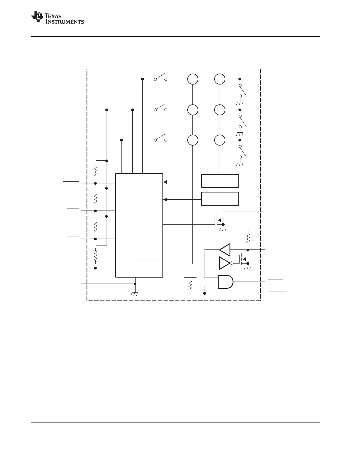
PG CS
S1
S4
PG CS
S2
S5
PG CS
S3
S6
CurrentLimit
ThermalLimit
Control
Logic
UVLO
POR
FAULT
AUXIN
Delay
PWR_GOOD_ALL
3.3VOUT
AUXOUT
1.5VOUT
OC
RCLKEN
PERST
SYSRST
3.3VIN
AUXIN
1.5VIN
CPUSB
CPPE
STBY
SHDN
GND
AUXIN
Note A:PG=powergood
NoteB:CS=currentsense
NoteC:TPS2231MRGP-2doesnothaveapull-upresistor.
(Note A)
(NoteC)
(NoteB)
www.ti.com
.................................................................................................................................................. SLVS536J –JULY 2004–REVISED SEPTEMBER 2009
FUNCTIONAL BLOCK DIAGRAM
Single ExpressCard Power Switch
TPS2231
TPS2236
Copyright © 2004–2009, Texas Instruments Incorporated Submit Documentation Feedback 9
Product Folder Link(s): TPS2231 TPS2236
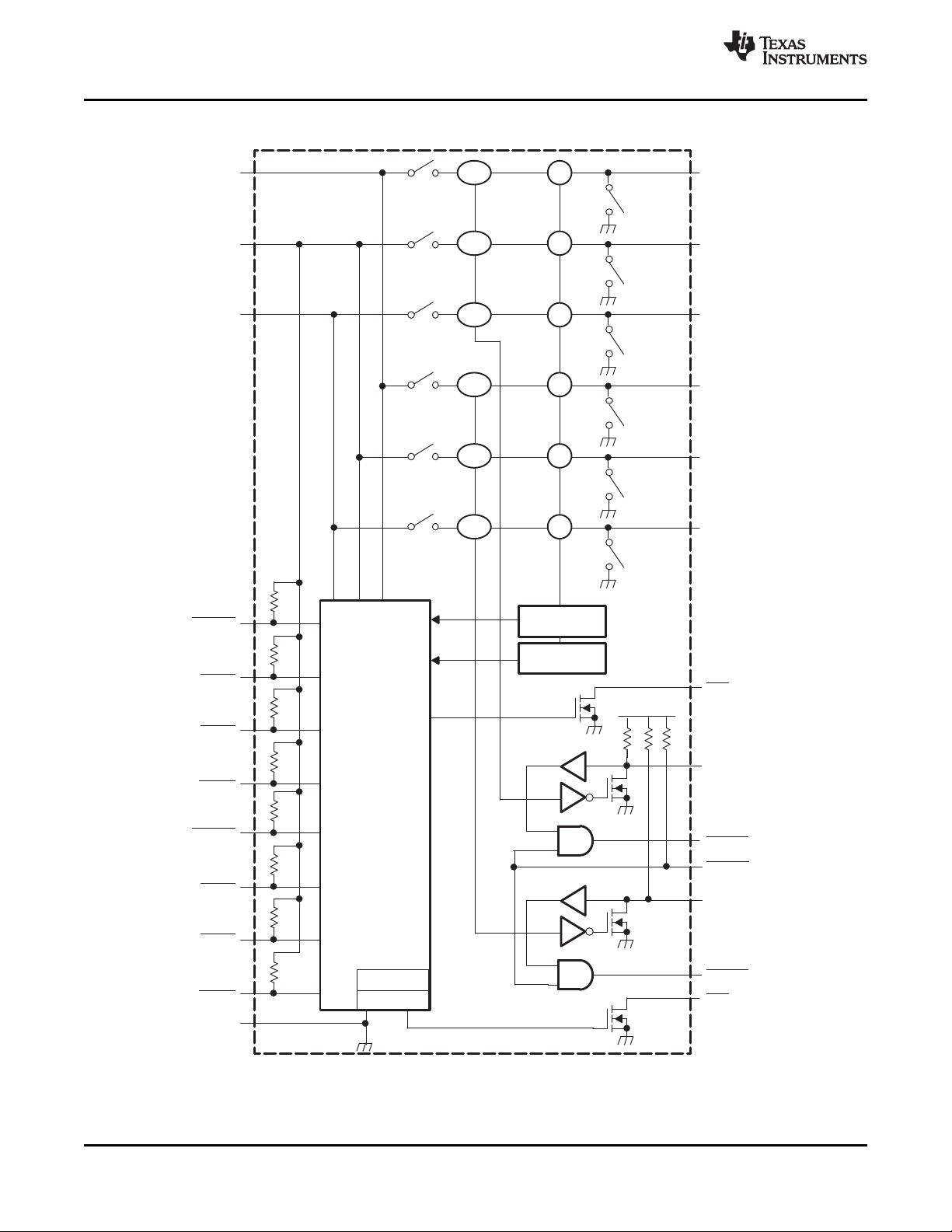
PG1 CS
S1
S4
S2
S5
S3
S6
Current Limit
Thermal Limit
Control
Logic
UVLO
POR
CHANNEL-1
FAULT
AUXIN
Delay
PWR_GOOD_ALL_2
3.3VOUT1
AUXOUT1
1.5 VOUT1
OC1
RCLKEN1
PERST1
SYSRST
3.3VIN
AUXIN
1.5VIN
CPUSB1
CPPE1
STBY1
SHDN1
GND
S7
S10
S8
S11
S9
S12
3.3VOUT2
AUXOUT2
1.5VOUT2
Delay
PWR_GOOD_ALL_1
CHANNEL-2
FAULT
RCLKEN2
PERST2
OC2
CPUSB2
CPPE2
STBY2
SHDN2
PG1 CS
PG1 CS
PG2 CS
PG2 CS
PG2 CS
TPS2231
TPS2236
SLVS536J –JULY 2004–REVISED SEPTEMBER 2009..................................................................................................................................................
Dual ExpressCard Power Switch
www.ti.com
10 Submit Documentation Feedback Copyright © 2004–2009, Texas Instruments Incorporated
Product Folder Link(s): TPS2231 TPS2236

TPS2231
TPS2236
www.ti.com
CPPE
A logic low level on this input indicates that the card present supports PCI Express functions. CPPE connects to
the AUXIN input through an internal pullup. When a card is inserted, CPPE is physically connected to ground if
the card supports PCI Express functions.
CPUSB
A logic low level on this input indicates that the card present supports USB functions. CPUSB connects to the
AUXIN input through an internal pullup. When a card is inserted, CPUSB is physically connected to ground if the
card supports USB functions.
SHDN
When asserted (logic low), this input instructs the power switch to turn off all voltage outputs and the discharge
FETs are activated. SHDN has an internal pullup connected to AUXIN.
STBY
When asserted (logic low) after the card is inserted, this input places the power switch in standby mode by
turning off the 3.3-V and 1.5-V power switches and keeping the AUX switch on. If asserted prior to the card being
present, STBY places the power switch in OFF Mode by turning off the AUX, 3.3-V, and 1.5-V power switches.
STBY has an internal pullup connected to AUXIN.
.................................................................................................................................................. SLVS536J –JULY 2004–REVISED SEPTEMBER 2009
DETAILED PIN DESCRIPTIONS
RCLKEN
This pin serves as both an input and an output. On power up, a discharge FET keeps this signal at a low state as
long as any of the output power rails are out of their tolerance range. Once all output power rails are within
tolerance, the switch releases RCLKEN allowing it to transition to a high state (internally pulled up to AUXIN).
The transition of RCLKEN from a low to a high state starts an internal timer for the purpose of deasserting
PERST. As an input, RCLKEN can be kept low to delay the start of the PERST internal timer.
Because RCLKEN is internally connected to a discharge FET, this pin can only be driven low and should never
be driven high as a logic input. When an external circuit drives this pin low, RCLKEN becomes an input;
otherwise, this pin is an output.
RCLKEN can be used by the host system to enable a clock driver.
PERST
On power up, this output remains asserted (logic level low) until all power rails are within tolerance. Once all
power rails are within tolerance and RCLKEN has been released (logic high), PERST is deasserted (logic high)
after a time delay as shown in the parametric table. On power down, this output is asserted whenever any of the
power rails drop below their voltage tolerance.
The PERST signal is an output from the host system and an input to the ExpressCard module. This signal is only
used by PCI Express-based modules and its function is to place the ExpressCard module in a reset state.
During power up, power down, or whenever power to the ExpressCard module is not stable or not within voltage
tolerance limits, the ExpressCard standard requires that PERST be asserted. As a result, this signal also serves
as a power-good indicator to the ExpressCard module, and the relationship between the power rails and PERST
are explicitly defined in the ExpressCard standard.
The host can also place the ExpressCard module in a reset state by asserting a system reset SYSRST. This
system reset generates a PERST to the ExpressCard module without disrupting the voltage rails. This is what is
normally called a warm reset. However, in a cold start situation, the system reset can also be used to extend the
length of time that PERST is asserted.
Copyright © 2004–2009, Texas Instruments Incorporated Submit Documentation Feedback 11
Product Folder Link(s): TPS2231 TPS2236
TPS2231
TPS2236
SLVS536J –JULY 2004–REVISED SEPTEMBER 2009..................................................................................................................................................
SYSRST
This input is driven by the host system and directly affects PERST. Asserting SYSRST (logic low) forces PERST
to assert. RCLKEN is not affected by the assertion of SYSRST. SYSRST has an internal pullup connected to
AUXIN.
OC
This pin is an open-drain output. When any of the three power switches (AUX, 3.3V, and 1.5V) is in an
overcurrent condition, OC is asserted (logic low) by an internal discharge FET with a deglitch delay. Otherwise,
the discharge FET is open, and the pin can be pulled up to a power supply through an external resistor.
FUNCTIONAL TRUTH TABLES
www.ti.com
VOLTAGE INPUTS
AUXIN 3.3VIN 1.5VIN SHDN STBY CP
Off x x x x x Off Off Off OFF
On x x 0 x x GND GND GND Shutdown
On x x 1 x 1 GND GND GND No Card
On On On 1 0 0 On Off Off Standby
On On On 1 1 0 On On On Card Inserted
(1) For input voltages, On means the respective input voltage is higher than its turnon threshold voltage; otherwise, the voltage is Off (for
AUX input,Off means the voltage is close to zero volt).
(2) For output voltages, On means the respective power switch is turned on so the input voltage is connected to the output; Off means the
power switch and its output discharge FET are both off; GND means the power switch is off but the output discharge FET is on so the
voltage on the output is pulled down to 0 V.
(3) Mode assigns each set of input conditions and respective output voltage results to a different name. These modes are referred to as
input conditions in the following Truth Table for Logic Outputs.
(4) CP = CPUSB and CPPE – equal to 1 when both CPUSB and CPPE signals are logic high, or equal to 0 when either CPUSB or CPPE is
low.
(1)
LOGIC INPUTS VOLTAGE OUTPUTS
(4)
AUXOUT 3.3VOUT 1.5VOUT
(2)
MODE
(3)
Truth Table for Logic Outputs
INPUT CONDITIONS LOGIC OUTPUTS
Truth Table for Voltage Outputs
MODE SYSRST RCLKEN
OFF
Shutdown
No Card
Standby
Card Inserted
(1) RCLKEN as a logic input in this column. RCLKEN is an I/O pin and it can be driven low externally, left open, or connected to
high-impedance terminals, such as the gate of a MOSFET. It must not be driven high externally.
(2) RCLKEN as a logic output in this column.
X X 0 0
0 Hi-Z 0 1
0 0 0 0
1 Hi-Z 1 1
1 0 0 0
(1)
PERST RCLKEN
(2)
12 Submit Documentation Feedback Copyright © 2004–2009, Texas Instruments Incorporated
Product Folder Link(s): TPS2231 TPS2236

TPS2231
TPS2236
www.ti.com
POWER STATES
If AUXIN is not present, then all input-to-output power switches are kept off (OFF mode).
If AUXIN is present and SHDN is asserted (logic low), then all input-to-output power switches are kept off and the
output discharge FETs are turned on (Shutdown mode). If SHDN is asserted and then de-asserted, the state on
the outputs is restored to the state prior to SHDN assertion.
If 3.3VIN, AUXIN and 1.5VIN are present at the input of the power switch and no card is inserted, then all
input-to-output power switches are kept off and the output discharge FETs are turned on (No Card mode).
If 3.3VIN, AUXIN and 1.5VIN are present at the input of the power switch prior to a card being inserted, then all
input-to-output power switches are turned on once a card-present signal (CPUSB and/or CPPE) is detected
(Card Inserted mode).
If a card is present and all output voltages are being applied, then the STBY is asserted (logic low); the AUXOUT
voltage is provided to the card, and the 3.3VOUT and 1.5VOUT switches are turned off (Standby mode).
If a card is present and all output voltages are being applied, then the 1.5VIN, or 3.3VIN is removed from the
input of the power switch; the AUXOUT voltage is provided to the card and the 3.3VOUT and 1.5VOUT switches
are turned off (Standby mode). TPS2231-3 only: If 3.3VIN is removed, the 3.3VOUT switch is turned off; and, the
1.5VOUT switch is unaffected. If 1.5VIN is removed, the 1.5VOUT switch is turned off; and, the 3.3VOUT switch
is unaffected.
If prior to the insertion of a card, the AUXIN is available at the input of the power switch and 3.3VIN and/or
1.5VIN are not, or if STBY is asserted (logic low), then no power is made available to the card (OFF mode). If
1.5VIN and 3.3VIN are made available at the input of the power switch after the card is inserted and STBY is not
asserted, all the output voltages are made available to the card (Card Inserted mode). TPS2231-3 only: If 1.5VIN
or 3.3VIN is made available at the input of the power switch after the card is inserted and STBY is not asserted,
all switches above their individual UVLO thresholds will turn on.
.................................................................................................................................................. SLVS536J –JULY 2004–REVISED SEPTEMBER 2009
DISCHARGE FETs
The discharge FETs on the outputs are activated whenever the device detects that a card is not present (No
Card mode). Activation occurs after the input-to-output power switches are turned off (break before make). The
discharge FETs de-activate if either of the card-present lines go active low, unless the SHDN pin is asserted.
The discharge FETs are also activated whenever the SHDN input is asserted and stay asserted until SHDN is
de-asserted.
Copyright © 2004–2009, Texas Instruments Incorporated Submit Documentation Feedback 13
Product Folder Link(s): TPS2231 TPS2236

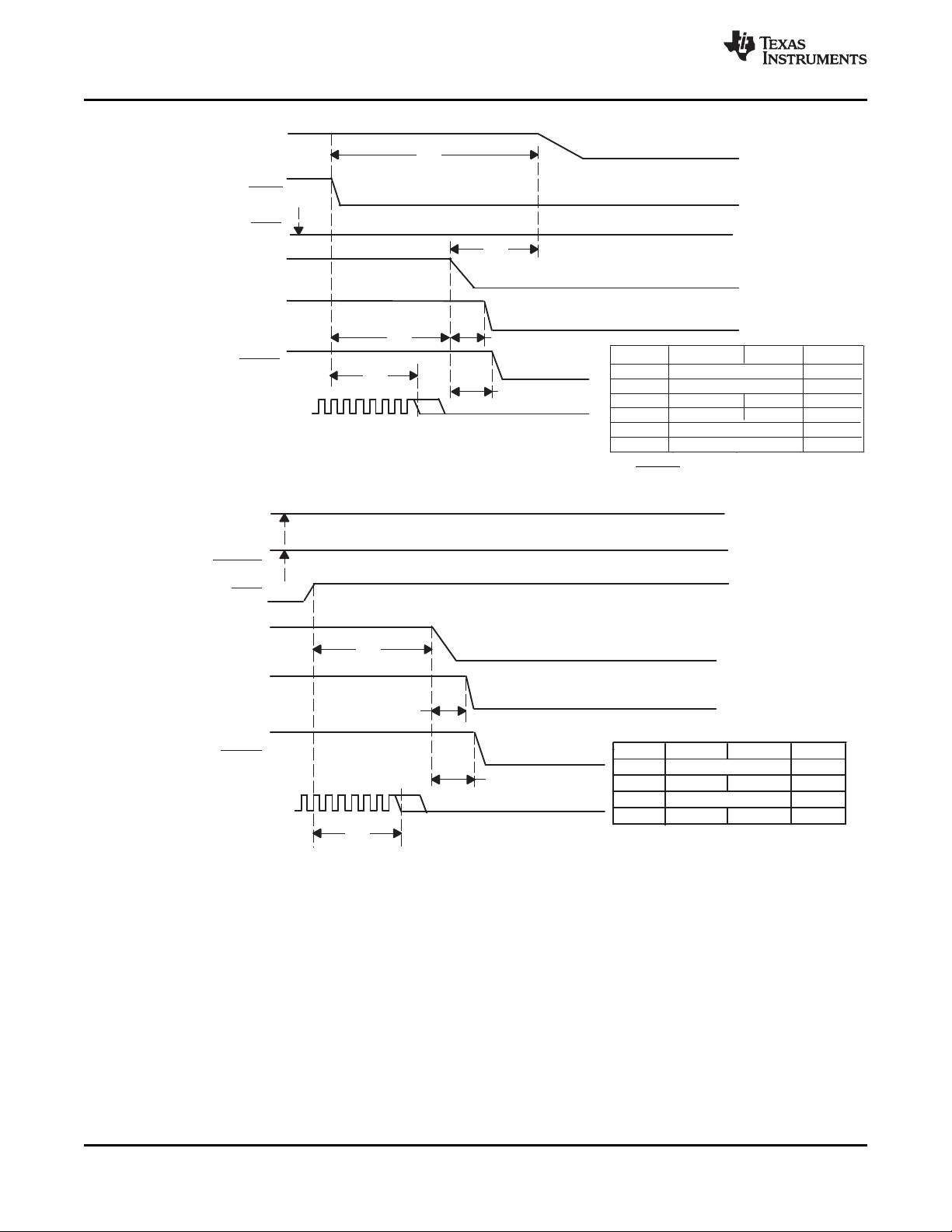
I
O(3.3VOUT/AUXOUT)
VIN
VIN
LOAD CIRCUIT LOAD CIRCUIT
50%
10%
VOLTAGE WAVEFORMS
10%
90%
C
L
I
O(1.5VOUT)
C
L
t
pd(off)
t
pd(on)
VIN
V
O(3.3VOUT/AUXOUT)
V
I(3.3V/AUXIN)
GND
V
I(3.3V)
GND
50%
10%
90%
t
pd(off)
t
pd(on)
VIN
V
O(1.5VOUT)
V
I(1.5V)
GND
V
I(1.5V)
GND
90%
Propagation Delay (1.5VOUT)Propagation Delay (3.3VOUT/AUXOUT)
t
r
t
f
V
O(3.3VOUT/AUXOUT)
V
I(3.3V)
GND
10%
90%
t
r
t
f
V
O(1.5VOUT)
GND
V
I(1.5V)
Rise/Fall Time (1.5VOUT)Rise/Fall Time (3.3VOUT/AUXOUT)
50%
10%
t
off
t
on
VIN
V
O(3.3VOUT/AUXOUT)
V
I(3.3V)
GND
V
I(3.3V)
GND
90%
50%
10%
t
off
t
on
VIN
V
O(1.5VOUT)
V
I(1.5V)
GND
V
I(1.5V)
GND
90%
Turn On/Off Time (1.5VOUT)Turn On/Off Time (3.3VOUT/AUXOUT)
R
L
R
L
TPS2231
TPS2236
SLVS536J –JULY 2004–REVISED SEPTEMBER 2009..................................................................................................................................................
PARAMETER MEASUREMENT INFORMATION
www.ti.com
Figure 1. Test Circuits and Voltage Waveforms
TYPICAL CHARACTERISTICS
14 Submit Documentation Feedback Copyright © 2004–2009, Texas Instruments Incorporated
Output voltage when card is inserted vs Time 2
RCLKEN and PERST voltage during power up vs Time 3
RCLKEN and PERST voltage during power down vs Time 4
PERST asserted by SYSRST when power is on vs Time 5
PERST de-asserted by SYSRST when power is on vs Time 6
Output voltage when 3.3VIN is removed vs Time 7
Output voltage when 1.5VIN is removed vs Time 8
OC response when powered into a short (3.3VOUT) vs Time 9
Supply current of AUXIN vs Junction temperature 10
Static drain-source on-state resistance vs Junction temperature 11
3.3-V power switch current limit vs Junction temperature 12
1.5-V power switch current limit vs Junction temperature 13
AUX power switch current limit vs Junction temperature 14
3.3-V power switch current limit trip vs Junction temperature 15
1.5-V power switch current limit trip vs Junction temperature 16
AUX power switch current limit trip vs Junction temperature 17
Table 1. Table of Graphs
Product Folder Link(s): TPS2231 TPS2236
FIGURE

V
O(3.3VOUT)
V
O(RCLKEN)
V
O(PERST)
t − Time − 5 ms/div
2 V/div
2 V/div
2 V/div
V
I(CPxx)
V
O(3.3VOUT)
V
O(1.5VOUT)
V
O(AUXOUT)
t − Time − 1 ms/div
2 V/div
2 V/div
2 V/div
2 V/div
V
O(AUXOUT)
V
O(RCLKEN)
V
O(PERST)
t − Time − 1 ms/div
2 V/div
2 V/div
2 V/div
V
O(PERST)
t − Time − 500 ns/div
V
I(SYSRST)
2 V/div
2 V/div
www.ti.com
TPS2231
TPS2236
.................................................................................................................................................. SLVS536J –JULY 2004–REVISED SEPTEMBER 2009
OUTPUT VOLTAGE WHEN CARD IS INSERTED RCLKEN AND PERST VOLTAGE DURING POWER UP
vs vs
TIME TIME
Figure 2. Figure 3.
RCLKEN AND PERST VOLTAGE DURING POWER DOWN PERST ASSERTED BY SYSRST WHEN POWER IS ON
vs vs
TIME TIME
Figure 4. Figure 5.
Copyright © 2004–2009, Texas Instruments Incorporated Submit Documentation Feedback 15
Product Folder Link(s): TPS2231 TPS2236

V
O(PERST)
t − Time − 100 ms/div
V
I(SYSRST)
2 V/div
2 V/div
V
O(3.3VOUT)
V
O(1.5VOUT)
V
O(AUXOUT)
V
I(3.3VIN)
R
L(3.3VOUT)
= 3.6 W
R
L(1.5VOUT)
= 2.7 W
R
L(AUXOUT)
= 12 W
C
L(3.3V/1.5V / AUXOUT)
= 68 mF
t − Time − 500 ms/div
2 V/div
2 V/div
2 V/div
2 V/div
V
O(3.3VOUT)
V
O(1.5VOUT)
V
I(1.5VIN)
t − Time − 500 ms/div
V
O(AUXVOUT)
R
L(3.3VOUT)
= 3.6 W
R
L(1.5VOUT)
= 2.7 W
R
L(AUXOUT)
= 12 W
C
L(3.3V/1.5V / AUXOUT)
= 68 mF
2 V/div
2 V/div
2 V/div
2 V/div
V
O(OC)
2 V/div
I
O(3.3VOUT)
0.5 A/div
t − Time − 5 ms/div
TPS2231
TPS2236
SLVS536J –JULY 2004–REVISED SEPTEMBER 2009..................................................................................................................................................
www.ti.com
PERST DE-ASSERTED BY SYSRST WHEN POWER IS ON OUTPUT VOLTAGE WHEN 3.3VIN IS REMOVED
vs vs
TIME TIME
Figure 6. Figure 7.
OUTPUT VOLTAGE WHEN 1.5VIN IS REMOVED OC RESPONSE WHEN POWERED INTO A SHORT (3.3VOUT)
vs vs
TIME TIME
Figure 8. Figure 9.
16 Submit Documentation Feedback Copyright © 2004–2009, Texas Instruments Incorporated
Product Folder Link(s): TPS2231 TPS2236

0
20
40
60
80
100
120
140
160
180
−40 −20 0 20 40 60 80 100 120
3.3V_AUX
1.5VIN
3.3VIN
On−State Resistance −
TJ − Junction Temperature − C
Ω
r
DS(on)
− Static Drain-Source
m
0
50
100
150
200
250
−40 −20 0 20 40 60 80 100 120
AUXIN + CPxx + SHDN+ RCLKEN
AUXIN + CPxx
AUXIN
CC
I Supply Current − − Aµ
TJ − Junction Temperature − C
1.90
1.95
2
2.05
2.10
−40 −20 0 20 40 60 80 100 120
Current Limit − A
TJ − Junction Temperature − C
900
910
920
930
940
950
960
970
980
990
1000
−40 −20 0 20 40 60 80 100 120
Current Limit − mA
TJ − Junction Temperature − C
www.ti.com
TPS2231
TPS2236
.................................................................................................................................................. SLVS536J –JULY 2004–REVISED SEPTEMBER 2009
SUPPLY CURRENT OF AUXIN STATIC DRAIN-SOURCE ON-STATE RESISTANCE
JUNCTION TEMPERATURE JUNCTION TEMPERATURE
3.3-V POWER SWITCH CURRENT LIMIT 1.5-V POWER SWITCH CURRENT LIMIT
JUNCTION TEMPERATURE JUNCTION TEMPERATURE
vs vs
Figure 10. Figure 11.
vs vs
Copyright © 2004–2009, Texas Instruments Incorporated Submit Documentation Feedback 17
Figure 12. Figure 13.
Product Folder Link(s): TPS2231 TPS2236

390
400
410
420
430
440
450
460
470
480
490
500
−40 −20 0 20 40 60 80 100 120
Current Limit − mA
TJ − Junction Temperature − C
2.50
2.60
2.70
2.80
2.90
3
3.10
3.20
−40 −20 0 20 40 60 80 100 120
Current Limit Trip Threshold − A
TJ − Junction Temperature − C
1000
1100
1200
1300
1400
1500
1600
1700
1800
1900
2000
−40 −20 0 20 40 60 80 100 120
Current Limit Trip Threshold − mA
TJ − Junction Temperature − C
600
640
680
720
760
800
−40 −20 0 20 40 60 80 100 120
Current Limit Trip Threshold − mA
TJ − Junction Temperature − C
TPS2231
TPS2236
SLVS536J –JULY 2004–REVISED SEPTEMBER 2009..................................................................................................................................................
www.ti.com
AUX POWER SWITCH CURRENT LIMIT 3.3-V POWER SWITCH CURRENT LIMIT TRIP
JUNCTION TEMPERATURE JUNCTION TEMPERATURE
1.5-V POWER SWITCH CURRENT LIMIT TRIP AUX POWER SWITCH CURRENT LIMIT TRIP
JUNCTION TEMPERATURE JUNCTION TEMPERATURE
vs vs
Figure 14. Figure 15.
vs vs
18 Submit Documentation Feedback Copyright © 2004–2009, Texas Instruments Incorporated
Figure 16. Figure 17.
Product Folder Link(s): TPS2231 TPS2236

TPS2231
TPS2236
www.ti.com
INTRODUCTION TO ExpressCard
An ExpressCard module is an add-in card with a serial interface based on PCI Express and/or Universal Serial
Bus (USB) technologies. An ExpressCard comes in two form factors defined as ExpressCard|34 or
ExpressCard|54. The difference, as defined by the name, is the width of the module, 34 mm or 54 mm,
respectively. Host systems supporting the ExpressCard module can support either the ExpressCard|34 or
ExpressCard|54 or both.
ExpressCard POWER REQUIREMENTS
Regardless of which ExpressCard module is used, the power requirements as defined in the ExpressCard
Standard apply to both on an individual slot basis. The host system is required to supply 3.3 V, 1.5 V, and AUX
to each of the ExpressCard slots. However, the voltage is only applied after an ExpressCard is inserted into the
slot.
The ExpressCard connector has two pins, CPPE and CPUSB, that are used to signal the host when a card is
inserted. If the ExpressCard module itself connects the CPPE to ground, the logic low level on that signal
indicates to the host that a card supporting PCI Express has been inserted. If CPUSB is connected to ground,
then the ExpressCard module supports the USB interface. If both PCI Express and USB are supported by the
ExpressCard module, then both signals, CPPE and CPUSB, must be connected to ground.
In addition to the Card Present signals (CPPE and CPUSB), the host system determines when to apply power to
the ExpressCard module based on the state of the system. The state of the system is defined by the state of the
3.3 V, 1.5 V, and AUX input voltage rails. For the sake of simplicity, the 3.3-V and 1.5-V rails are defined as the
primary voltage rails as oppose to the auxiliary voltage rail, AUX.
.................................................................................................................................................. SLVS536J –JULY 2004–REVISED SEPTEMBER 2009
APPLICATION INFORMATION
ExpressCard POWER SWITCH OPERATION
The ExpressCard power switch resides on the host, and its main function is to control when to send power to the
ExpressCard slot. The ExpressCard power switch makes decisions based on the Card Present inputs and on the
state of the host system as defined by the primary and auxiliary voltage rails.
The following conditions define the operation of the host power controller:
1. When both primary power and auxiliary power at the input of the ExpressCard power switch are off, then all
power to the ExpressCard connector is off regardless of whether a card is present.
2. When both primary power and auxiliary power at the input of the ExpressCard power switch are on, then
power is only applied to the ExpressCard after the ExpressCard power switch detects that a card is present.
3. When primary power (either +3.3 V or +1.5 V) at the input of the ExpressCard power switch is off and
auxiliary power at the input of the ExpressCard power switch is on, then the ExpressCard power switch
behaves in the following manner:
(a) If neither of the Card Present inputs is detected (no card inserted), then no power is applied to the
ExpressCard slot.
(b) If the card is inserted after the system has entered this power state, then no power is applied to the
ExpressCard slot.
(c) If the card is inserted prior to the removal of the primary power (either +3.3 V or +1.5 V or both) at the
input of the ExpressCard power switch, then only the primary power (both +3.3 V and +1.5 V) is removed
and the auxiliary power is sent to the ExpressCard slot.
Figure 18 through Figure 23 illustrate the timing relationships between power/logic inputs and outputs of
ExpressCard.
Copyright © 2004–2009, Texas Instruments Incorporated Submit Documentation Feedback 19
Product Folder Link(s): TPS2231 TPS2236

b
Tpd
Min Max
Units
a
b 100
c
d
e
100
f
4
20
ms
g
10 ms
a
g c d
e
f
SYSRST
CPxx
Host Power
(AUXIN, 3.3VIN,
and 1.5VIN)
Card Power
(AUXIN, 3.3VOUT,
and 1.5VOUT)
RCLKEN
PERST
REFCLK
System Dependent
System Dependent
System Dependent
ms
ms
a
b c d
e
SYSRST
CPxx
Host Power
(AUXIN, 3.3VIN,
and 1.5VIN)
Card Power
(AUXIN, 3.3VOUT,
and 1.5VOUT)
RCLKEN
PERST
REFCLK
Tpd
Min Max
Units
a
b
100
c
d
e
4
20
ms
10 ms
System Dependent
System Dependent
ms
TPS2231
TPS2236
SLVS536J –JULY 2004–REVISED SEPTEMBER 2009..................................................................................................................................................
EXPRESS CARD TIMING DIAGRAMS
www.ti.com
Figure 18. Timing Signals - Card Present Before Host Power Is On
Figure 19. Timing Signals - Host Power Is On Prior to Card Insertion
20 Submit Documentation Feedback Copyright © 2004–2009, Texas Instruments Incorporated
Product Folder Link(s): TPS2231 TPS2236

SYSRST
CPxx
RCLKEN
PERST
REFCLK
(Either Tri-Stated or Off)
Host Power
(AUXIN)
Host Power
(3.3VIN and 1.5VIN)
Card Power
(AUXIN, 3.3VOUT,
and 1.5VOUT)
Note: Once 3.3 V and 1.5 V are applied, the power switch follows the power-up sequence of Figure 18 or Figure 19.
SYSRST
CPxx
RCLKEN
REFCLK
Host Power
(AUXIN, 3.3VIN, and 1.5VIN)
Card Power
(AUXOUT, 3.3VOUT, and 1.5VOUT)
PERST
c
d
e
a
a
Tpd
Min Max
Units
a
b
500
c
d
e 500
ns
System Dependent
System Dependent
ns
Load Dependent
www.ti.com
TPS2231
TPS2236
.................................................................................................................................................. SLVS536J –JULY 2004–REVISED SEPTEMBER 2009
Figure 20. Timing Signals - Host System In Standby Prior to Card Insertion
Figure 21. Timing Signals - Host-Controlled Power Down
Copyright © 2004–2009, Texas Instruments Incorporated Submit Documentation Feedback 21
Product Folder Link(s): TPS2231 TPS2236
e
f
a
d
f
SHDN
CPxx
RCLKEN
REFCLK
Host Power
(AUXIN, 3.3VIN, and 1.5VIN)
Card Power
(AUXOUT, 3.3VOUT, and 1.5VOUT)
PERST
Tpd
Min Max
Units
a
b
c
d
e
f
500
ns
System Dependent
System Dependent
System Dependent
500
Load Dependent
ns
c
Tpd Min Max Units
a
b
500
ns
c
d
500
a
d
b
c
Load Dependent
System Dependent
ns
SYSRST
CPxx
RCLKEN
REFCLK
Host Power
(AUXIN, 3.3VIN, and 1.5VIN)
Card Power
(AUXOUT, 3.3VOUT, and 1.5VOUT)
PERST
TPS2231
TPS2236
SLVS536J –JULY 2004–REVISED SEPTEMBER 2009..................................................................................................................................................
Figure 22. Timing Signals - Controlled Power Down When SHDN Asserted
www.ti.com
22 Submit Documentation Feedback Copyright © 2004–2009, Texas Instruments Incorporated
Figure 23. Timing Signals - Surprise Card Removal
Product Folder Link(s): TPS2231 TPS2236

TPS2231
TPS2236
www.ti.com
NOTE: Page numbers in the latest revision may differ from previous versions.
Changes from Revision F (August 2007) to Revision G ................................................................................................ Page
• Changed note
(1) The TPS2231MRGP is identical to the TPS2231 with the exception of the PowerPAD dimensions. See the Thermal Pad Mechanical
Changes from Revision G (August 2007) to Revision H ................................................................................................ Page
• Changed From; reel is rotated 90°C To: reel is rotated 180°C ............................................................................................ 2
Changes from Revision H (September 2007) to Revision I ............................................................................................ Page
• Added TPS2231MRGP-2 and
• Added TPS2231, TPS2231-1, and TPS2231-1 values to the Logic input supply current .................................................... 4
• Added Note C to the Function Block Diagram ...................................................................................................................... 9
.................................................................................................................................................. SLVS536J –JULY 2004–REVISED SEPTEMBER 2009
REVISION HISTORY
(1)
of the Available Options table. .................................................................................................................. 2
data portion of this data sheet for specific information. The thermal pad for the TPS2231MRGP and TPS2231MRGP-1 is 2,2 mm × 2,2
mm; the thermal pad for the TPS2231RGP is 2,7 mm × 2,7 mm.
(2)
to the Available Options table. ......................................................................................... 2
(2) The TPS2231MRGP-2 is identical to the TPS2231MRGP with the exception that the orientation of the part in the reel is rotated 90° and
does not have an internal pull-up resistor between AUX IN and SYSRST. See the Package Materials Information portion of this data
sheet for specific information.
Changes from Revision I (November 2007) to Revision J ............................................................................................. Page
• Added TPS2231-3 to the Available Options table. ............................................................................................................... 2
• Added explanatory footnote to Available Options table regarding TPS2231MRGP-3 ......................................................... 2
• Added TPS2231-3 test condition statement to UVLO spec. ................................................................................................ 5
• Added power state explanation for TPS2231-3 device. ..................................................................................................... 13
Copyright © 2004–2009, Texas Instruments Incorporated Submit Documentation Feedback 23
Product Folder Link(s): TPS2231 TPS2236

PACKAGE OPTION ADDENDUM
www.ti.com
PACKAGING INFORMATION
Orderable Device Status
TPS2231MRGPR ACTIVE QFN RGP 20 3000 Green (RoHS
TPS2231MRGPR-1 ACTIVE QFN RGP 20 3000 Green (RoHS
TPS2231MRGPR-1G4 ACTIVE QFN RGP 20 3000 Green (RoHS
TPS2231MRGPR-2 ACTIVE QFN RGP 20 3000 Green (RoHS
TPS2231MRGPR-2G4 ACTIVE QFN RGP 20 3000 Green (RoHS
TPS2231MRGPR-3 ACTIVE QFN RGP 20 3000 Green (RoHS
TPS2231MRGPRG4 ACTIVE QFN RGP 20 3000 Green (RoHS
TPS2231MRGPT ACTIVE QFN RGP 20 250 Green (RoHS
TPS2231MRGPT-1 ACTIVE QFN RGP 20 250 Green (RoHS
TPS2231MRGPT-1G4 ACTIVE QFN RGP 20 250 Green (RoHS
TPS2231MRGPT-3 ACTIVE QFN RGP 20 250 Green (RoHS
TPS2231MRGPTG4 ACTIVE QFN RGP 20 250 Green (RoHS
TPS2231PW ACTIVE TSSOP PW 20 70 Green (RoHS
TPS2231PWG4 ACTIVE TSSOP PW 20 70 Green (RoHS
TPS2231PWP ACTIVE HTSSOP PWP 24 60 Green (RoHS
TPS2231PWPG4 ACTIVE HTSSOP PWP 24 60 Green (RoHS
TPS2231PWPR ACTIVE HTSSOP PWP 24 2000 Green (RoHS
Package Type Package
(1)
Drawing
Pins Package
Qty
Eco Plan
(2)
& no Sb/Br)
& no Sb/Br)
& no Sb/Br)
& no Sb/Br)
& no Sb/Br)
& no Sb/Br)
& no Sb/Br)
& no Sb/Br)
& no Sb/Br)
& no Sb/Br)
& no Sb/Br)
& no Sb/Br)
& no Sb/Br)
& no Sb/Br)
& no Sb/Br)
& no Sb/Br)
& no Sb/Br)
Lead/Ball Finish MSL Peak Temp
(3)
CU NIPDAU Level-2-260C-1 YEAR -40 to 85 2231M
CU NIPDAU Level-2-260C-1 YEAR -40 to 85 2231M
CU NIPDAU Level-2-260C-1 YEAR -40 to 85 2231M
CU NIPDAU Level-2-260C-1 YEAR -40 to 85 2231-2
CU NIPDAU Level-2-260C-1 YEAR -40 to 85 2231-2
CU NIPDAU Level-2-260C-1 YEAR -40 to 85 2231-3
CU NIPDAU Level-2-260C-1 YEAR -40 to 85 2231M
CU NIPDAU Level-2-260C-1 YEAR -40 to 85 2231M
CU NIPDAU Level-2-260C-1 YEAR -40 to 85 2231M
CU NIPDAU Level-2-260C-1 YEAR -40 to 85 2231M
CU NIPDAU Level-2-260C-1 YEAR -40 to 85 2231-3
CU NIPDAU Level-2-260C-1 YEAR -40 to 85 2231M
CU NIPDAU Level-1-260C-UNLIM -40 to 85 TPS2231
CU NIPDAU Level-1-260C-UNLIM -40 to 85 TPS2231
CU NIPDAU Level-2-260C-1 YEAR -40 to 85 TPS2231
CU NIPDAU Level-2-260C-1 YEAR -40 to 85 TPS2231
CU NIPDAU Level-2-260C-1 YEAR -40 to 85 TPS2231
Op Temp (°C) Top-Side Markings
11-Apr-2013
Samples
(4)
Addendum-Page 1

PACKAGE OPTION ADDENDUM
www.ti.com
Orderable Device Status
Package Type Package
(1)
Drawing
Pins Package
Qty
TPS2231PWPRG4 ACTIVE HTSSOP PWP 24 2000 Green (RoHS
Eco Plan
(2)
Lead/Ball Finish MSL Peak Temp
(3)
Op Temp (°C) Top-Side Markings
CU NIPDAU Level-2-260C-1 YEAR -40 to 85 TPS2231
(4)
11-Apr-2013
& no Sb/Br)
TPS2231PWR ACTIVE TSSOP PW 20 2000 Green (RoHS
CU NIPDAU Level-1-260C-UNLIM -40 to 85 TPS2231
& no Sb/Br)
TPS2231PWRG4 ACTIVE TSSOP PW 20 2000 Green (RoHS
CU NIPDAU Level-1-260C-UNLIM -40 to 85 TPS2231
& no Sb/Br)
TPS2231RGPR ACTIVE QFN RGP 20 3000 Green (RoHS
CU NIPDAU Level-2-260C-1 YEAR -40 to 85 2231
& no Sb/Br)
TPS2231RGPRG4 ACTIVE QFN RGP 20 3000 Green (RoHS
CU NIPDAU Level-2-260C-1 YEAR -40 to 85 2231
& no Sb/Br)
TPS2231RGPT ACTIVE QFN RGP 20 250 Green (RoHS
CU NIPDAU Level-2-260C-1 YEAR 2231
& no Sb/Br)
TPS2231RGPTG4 ACTIVE QFN RGP 20 250 Green (RoHS
CU NIPDAU Level-2-260C-1 YEAR 2231
& no Sb/Br)
TPS2236DAP ACTIVE HTSSOP DAP 32 46 Green (RoHS
CU NIPDAU Level-3-260C-168 HR -40 to 85 TPS2236
& no Sb/Br)
TPS2236DAPG4 ACTIVE HTSSOP DAP 32 46 Green (RoHS
CU NIPDAU Level-3-260C-168 HR -40 to 85 TPS2236
& no Sb/Br)
TPS2236DAPR ACTIVE HTSSOP DAP 32 2000 Green (RoHS
CU NIPDAU Level-3-260C-168 HR -40 to 85 TPS2236
& no Sb/Br)
TPS2236DAPRG4 ACTIVE HTSSOP DAP 32 2000 Green (RoHS
CU NIPDAU Level-3-260C-168 HR -40 to 85 TPS2236
& no Sb/Br)
(1)
The marketing status values are defined as follows:
ACTIVE: Product device recommended for new designs.
LIFEBUY: TI has announced that the device will be discontinued, and a lifetime-buy period is in effect.
NRND: Not recommended for new designs. Device is in production to support existing customers, but TI does not recommend using this part in a new design.
PREVIEW: Device has been announced but is not in production. Samples may or may not be available.
OBSOLETE: TI has discontinued the production of the device.
(2)
Eco Plan - The planned eco-friendly classification: Pb-Free (RoHS), Pb-Free (RoHS Exempt), or Green (RoHS & no Sb/Br) - please check http://www.ti.com/productcontent for the latest availability
information and additional product content details.
TBD: The Pb-Free/Green conversion plan has not been defined.
Pb-Free (RoHS): TI's terms "Lead-Free" or "Pb-Free" mean semiconductor products that are compatible with the current RoHS requirements for all 6 substances, including the requirement that
lead not exceed 0.1% by weight in homogeneous materials. Where designed to be soldered at high temperatures, TI Pb-Free products are suitable for use in specified lead-free processes.
Pb-Free (RoHS Exempt): This component has a RoHS exemption for either 1) lead-based flip-chip solder bumps used between the die and package, or 2) lead-based die adhesive used between
the die and leadframe. The component is otherwise considered Pb-Free (RoHS compatible) as defined above.
Samples
Addendum-Page 2

PACKAGE OPTION ADDENDUM
www.ti.com
Green (RoHS & no Sb/Br): TI defines "Green" to mean Pb-Free (RoHS compatible), and free of Bromine (Br) and Antimony (Sb) based flame retardants (Br or Sb do not exceed 0.1% by weight
in homogeneous material)
11-Apr-2013
(3)
MSL, Peak Temp. -- The Moisture Sensitivity Level rating according to the JEDEC industry standard classifications, and peak solder temperature.
(4)
Multiple Top-Side Markings will be inside parentheses. Only one Top-Side Marking contained in parentheses and separated by a "~" will appear on a device. If a line is indented then it is a
continuation of the previous line and the two combined represent the entire Top-Side Marking for that device.
Important Information and Disclaimer:The information provided on this page represents TI's knowledge and belief as of the date that it is provided. TI bases its knowledge and belief on information
provided by third parties, and makes no representation or warranty as to the accuracy of such information. Efforts are underway to better integrate information from third parties. TI has taken and
continues to take reasonable steps to provide representative and accurate information but may not have conducted destructive testing or chemical analysis on incoming materials and chemicals.
TI and TI suppliers consider certain information to be proprietary, and thus CAS numbers and other limited information may not be available for release.
In no event shall TI's liability arising out of such information exceed the total purchase price of the TI part(s) at issue in this document sold by TI to Customer on an annual basis.
Addendum-Page 3

PACKAGE MATERIALS INFORMATION
www.ti.com 14-Mar-2014
TAPE AND REEL INFORMATION
*All dimensions are nominal
Device Package
TPS2231MRGPR QFN RGP 20 3000 330.0 12.4 4.25 4.25 1.15 8.0 12.0 Q2
TPS2231MRGPR QFN RGP 20 3000 330.0 12.4 4.25 4.25 1.15 8.0 12.0 Q2
TPS2231MRGPR-1 QFN RGP 20 3000 330.0 12.4 4.25 4.25 1.15 8.0 12.0 Q3
TPS2231MRGPR-2 QFN RGP 20 3000 330.0 12.4 4.25 4.25 1.15 8.0 12.0 Q1
TPS2231MRGPR-3 QFN RGP 20 3000 330.0 12.4 4.25 4.25 1.15 8.0 12.0 Q2
TPS2231MRGPT QFN RGP 20 250 180.0 12.4 4.25 4.25 1.15 8.0 12.0 Q2
TPS2231MRGPT QFN RGP 20 250 180.0 12.4 4.25 4.25 1.15 8.0 12.0 Q2
TPS2231MRGPT-1 QFN RGP 20 250 180.0 12.4 4.25 4.25 1.15 8.0 12.0 Q3
TPS2231MRGPT-3 QFN RGP 20 250 180.0 12.4 4.25 4.25 1.15 8.0 12.0 Q2
TPS2231PWPR HTSSOP PWP 24 2000 330.0 16.4 6.95 8.3 1.6 8.0 16.0 Q1
TPS2231PWR TSSOP PW 20 2000 330.0 16.4 6.95 7.1 1.6 8.0 16.0 Q1
TPS2231RGPR QFN RGP 20 3000 330.0 12.4 4.25 4.25 1.15 8.0 12.0 Q2
TPS2231RGPT QFN RGP 20 250 180.0 12.4 4.25 4.25 1.15 8.0 12.0 Q2
TPS2236DAPR HTSSOP DAP 32 2000 330.0 24.4 8.6 11.5 1.6 12.0 24.0 Q1
Type
Package
Drawing
Pins SPQ Reel
Diameter
(mm)
Reel
Width
W1 (mm)
A0
(mm)B0(mm)K0(mm)P1(mm)W(mm)
Pin1
Quadrant
Pack Materials-Page 1
PACKAGE MATERIALS INFORMATION
www.ti.com 14-Mar-2014
*All dimensions are nominal
Device Package Type Package Drawing Pins SPQ Length (mm) Width (mm) Height (mm)
TPS2231MRGPR QFN RGP 20 3000 367.0 367.0 35.0
TPS2231MRGPR QFN RGP 20 3000 367.0 367.0 35.0
TPS2231MRGPR-1 QFN RGP 20 3000 367.0 367.0 35.0
TPS2231MRGPR-2 QFN RGP 20 3000 367.0 367.0 35.0
TPS2231MRGPR-3 QFN RGP 20 3000 367.0 367.0 35.0
TPS2231MRGPT QFN RGP 20 250 210.0 185.0 35.0
TPS2231MRGPT QFN RGP 20 250 210.0 185.0 35.0
TPS2231MRGPT-1 QFN RGP 20 250 210.0 185.0 35.0
TPS2231MRGPT-3 QFN RGP 20 250 210.0 185.0 35.0
TPS2231PWPR HTSSOP PWP 24 2000 367.0 367.0 38.0
TPS2231PWR TSSOP PW 20 2000 367.0 367.0 38.0
TPS2231RGPR QFN RGP 20 3000 367.0 367.0 35.0
TPS2231RGPT QFN RGP 20 250 210.0 185.0 35.0
TPS2236DAPR HTSSOP DAP 32 2000 367.0 367.0 45.0
Pack Materials-Page 2


IMPORTANT NOTICE
Texas Instruments Incorporated and its subsidiaries (TI) reserve the right to make corrections, enhancements, improvements and other
changes to its semiconductor products and services per JESD46, latest issue, and to discontinue any product or service per JESD48, latest
issue. Buyers should obtain the latest relevant information before placing orders and should verify that such information is current and
complete. All semiconductor products (also referred to herein as “components”) are sold subject to TI’s terms and conditions of sale
supplied at the time of order acknowledgment.
TI warrants performance of its components to the specifications applicable at the time of sale, in accordance with the warranty in TI’s terms
and conditions of sale of semiconductor products. Testing and other quality control techniques are used to the extent TI deems necessary
to support this warranty. Except where mandated by applicable law, testing of all parameters of each component is not necessarily
performed.
TI assumes no liability for applications assistance or the design of Buyers’ products. Buyers are responsible for their products and
applications using TI components. To minimize the risks associated with Buyers’ products and applications, Buyers should provide
adequate design and operating safeguards.
TI does not warrant or represent that any license, either express or implied, is granted under any patent right, copyright, mask work right, or
other intellectual property right relating to any combination, machine, or process in which TI components or services are used. Information
published by TI regarding third-party products or services does not constitute a license to use such products or services or a warranty or
endorsement thereof. Use of such information may require a license from a third party under the patents or other intellectual property of the
third party, or a license from TI under the patents or other intellectual property of TI.
Reproduction of significant portions of TI information in TI data books or data sheets is permissible only if reproduction is without alteration
and is accompanied by all associated warranties, conditions, limitations, and notices. TI is not responsible or liable for such altered
documentation. Information of third parties may be subject to additional restrictions.
Resale of TI components or services with statements different from or beyond the parameters stated by TI for that component or service
voids all express and any implied warranties for the associated TI component or service and is an unfair and deceptive business practice.
TI is not responsible or liable for any such statements.
Buyer acknowledges and agrees that it is solely responsible for compliance with all legal, regulatory and safety-related requirements
concerning its products, and any use of TI components in its applications, notwithstanding any applications-related information or support
that may be provided by TI. Buyer represents and agrees that it has all the necessary expertise to create and implement safeguards which
anticipate dangerous consequences of failures, monitor failures and their consequences, lessen the likelihood of failures that might cause
harm and take appropriate remedial actions. Buyer will fully indemnify TI and its representatives against any damages arising out of the use
of any TI components in safety-critical applications.
In some cases, TI components may be promoted specifically to facilitate safety-related applications. With such components, TI’s goal is to
help enable customers to design and create their own end-product solutions that meet applicable functional safety standards and
requirements. Nonetheless, such components are subject to these terms.
No TI components are authorized for use in FDA Class III (or similar life-critical medical equipment) unless authorized officers of the parties
have executed a special agreement specifically governing such use.
Only those TI components which TI has specifically designated as military grade or “enhanced plastic” are designed and intended for use in
military/aerospace applications or environments. Buyer acknowledges and agrees that any military or aerospace use of TI components
which have not been so designated is solely at the Buyer's risk, and that Buyer is solely responsible for compliance with all legal and
regulatory requirements in connection with such use.
TI has specifically designated certain components as meeting ISO/TS16949 requirements, mainly for automotive use. In any case of use of
non-designated products, TI will not be responsible for any failure to meet ISO/TS16949.
Products Applications
Audio www.ti.com/audio Automotive and Transportation www.ti.com/automotive
Amplifiers amplifier.ti.com Communications and Telecom www.ti.com/communications
Data Converters dataconverter.ti.com Computers and Peripherals www.ti.com/computers
DLP® Products www.dlp.com Consumer Electronics www.ti.com/consumer-apps
DSP dsp.ti.com Energy and Lighting www.ti.com/energy
Clocks and Timers www.ti.com/clocks Industrial www.ti.com/industrial
Interface interface.ti.com Medical www.ti.com/medical
Logic logic.ti.com Security www.ti.com/security
Power Mgmt power.ti.com Space, Avionics and Defense www.ti.com/space-avionics-defense
Microcontrollers microcontroller.ti.com Video and Imaging www.ti.com/video
RFID www.ti-rfid.com
OMAP Applications Processors www.ti.com/omap TI E2E Community e2e.ti.com
Wireless Connectivity www.ti.com/wirelessconnectivity
Mailing Address: Texas Instruments, Post Office Box 655303, Dallas, Texas 75265
Copyright © 2014, Texas Instruments Incorporated

 Loading...