

TPS2212
SINGLE-SLOT, PARALLEL INTERFACE POWER SWITCH
FOR LOW POWER PC CARD SLOTS
SLVS193 – APRIL 1999
1
POST OFFICE BOX 655303 • DALLAS, TEXAS 75265
D
Fully Integrated VCC and Vpp Switching for
Low Power Single-Slot PC Card Interface
D
Low r
DS(on)
(160-mΩ VCC Switches)
D
Low Current Limit, 450 mA (VCC) Typ
D
3.3-V Low-Voltage Mode
D
12-V Supply Can Be Disabled Except
During 12-V Flash Programming
D
Short-Circuit and Thermal Protection
D
Space-Saving 16-Pin SSOP (DB)
D
Compatible With 3.3-V, 5-V, and 12-V PC
Cards
D
Break-Before-Make Switching
D
Typical Applications Include: PCMCIA PC
Card Sockets in PDAs, PBXs, Bar Code
Scanners, Compact Flash and Smart Cards
description
The TPS2212 PC Card power-interface switch provides an integrated power-management solution for a single
low power PC Card. All of the discrete power MOSFET s, a logic section, current limiting, and thermal protection
for PC Card control are combined on a single integrated circuit, using the Texas Instruments LinBiCMOS
process. The circuit allows the distribution of 3.3-V , 5-V, and/or 12-V card power , and is compatible with many
PCMCIA controllers. The current-limiting feature eliminates the need for fuses, which reduces component count
and improves reliability. Current-limit reporting can help the user isolate a system fault to the PC Card.
The TPS2212 features a 3.3-V low-voltage mode that allows for 3.3-V switching without the need for 5 V . Bias
power can be derived from either the 3.3-V or 5-V inputs. This facilitates low-power system designs such as
sleep mode and pager mode, where only 3.3 V is available.
End equipment for the TPS2212 includes notebook computers, desktop computers, personal digital assistants
(PDAs), digital cameras, and bar-code scanners. This device is well suited for those applications which need to
limit the power provided to the PC card due to power supply constraints. In many applications, such as palm
computers, the system cannot allocate more than 200 mA of current to a PC card slot. For these lower power
applications, the TPS2212 provides the same advanced level of protection as the TPS221 1 provides for higher
power applications.
AVAILABLE OPTIONS
PACKAGED DEVICE
T
A
SMALL OUTLINE
(DB)
–40°C to 85°C TPS2212IDBLE
The DB package is only available left-end taped
and reeled (indicated by the LE suffix on the
device type, e.g. TPS2212IDBLE).
Copyright 1999, Texas Instruments Incorporated
PRODUCTION DATA information is current as of publication date.
Products conform to specifications per the terms of Texas Instruments
standard warranty. Production processing does not necessarily include
testing of all parameters.
Please be aware that an important notice concerning availability, standard warranty, and use in critical applications of
Texas Instruments semiconductor products and disclaimers thereto appears at the end of this data sheet.
PC Card is a trademark of PCMCIA (Personal Computer Memory Card International Association).
LinBiCMOS is a trademark of Texas Instruments Incorporated.
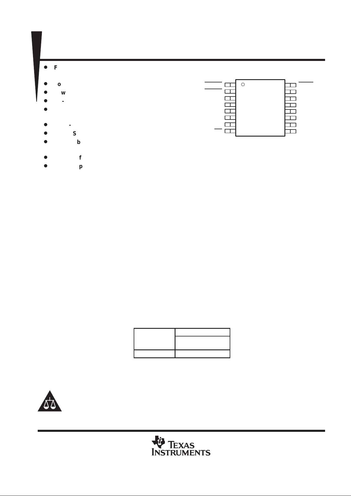
1
2
3
4
5
6
7
8
16
15
14
13
12
11
10
9
VCCD0
VCCD1
3.3V
3.3V
5V
5V
GND
OC
SHDN
VPPD0
VPPD1
VCC
VCC
VCC
VPP
VPPI
DB PACKAGE
(TOP VIEW)
TPS2212
SINGLE-SLOT, PARALLEL INTERFACE POWER SWITCH
FOR LOW POWER PC CARD SLOTS
SLVS193 – APRIL 1999
2
POST OFFICE BOX 655303 • DALLAS, TEXAS 75265
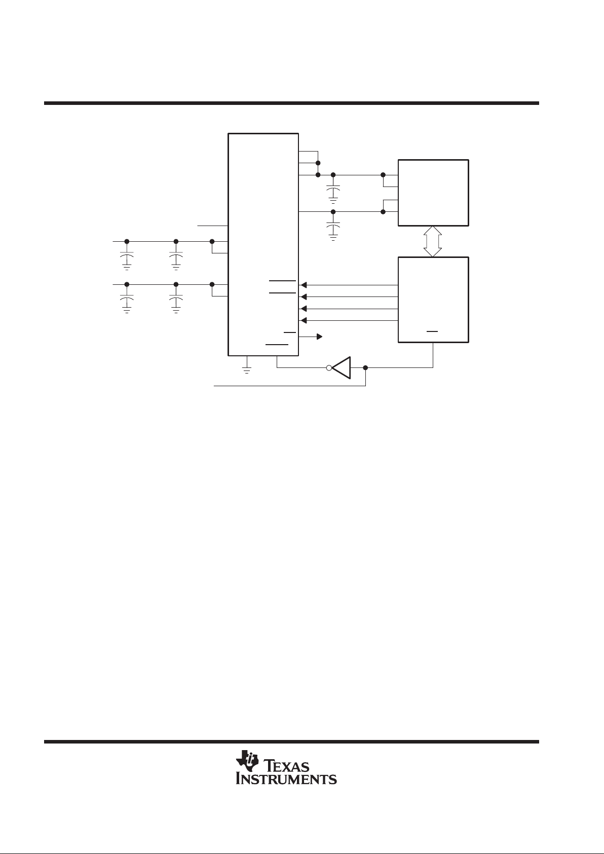
typical PC-card power-distribution application
VCC
VCC
VCC
VPP
VCCD0
VCCD1
VPPD0
VPPD1
OC
SHDNGND
0.1 µF
0.1 µF
V
CC1
V
CC2
V
pp1
V
pp2
PC Card
Connector
PCMCIA
Controller
VCC_EN0
VCC_EN1
VPP_EN0
VPP_EN1
CS
To CPU
TPS2212
VPPI
5V
5V
1 µF0.1 µF
5 V
3.3V
3.3V
1 µF0.1 µF
3.3 V
Shutdown Signal From CPU
3.3 V–12 V
TPS2212
SINGLE-SLOT, PARALLEL INTERFACE POWER SWITCH
FOR LOW POWER PC CARD SLOTS
SLVS193 – APRIL 1999
3
POST OFFICE BOX 655303 • DALLAS, TEXAS 75265
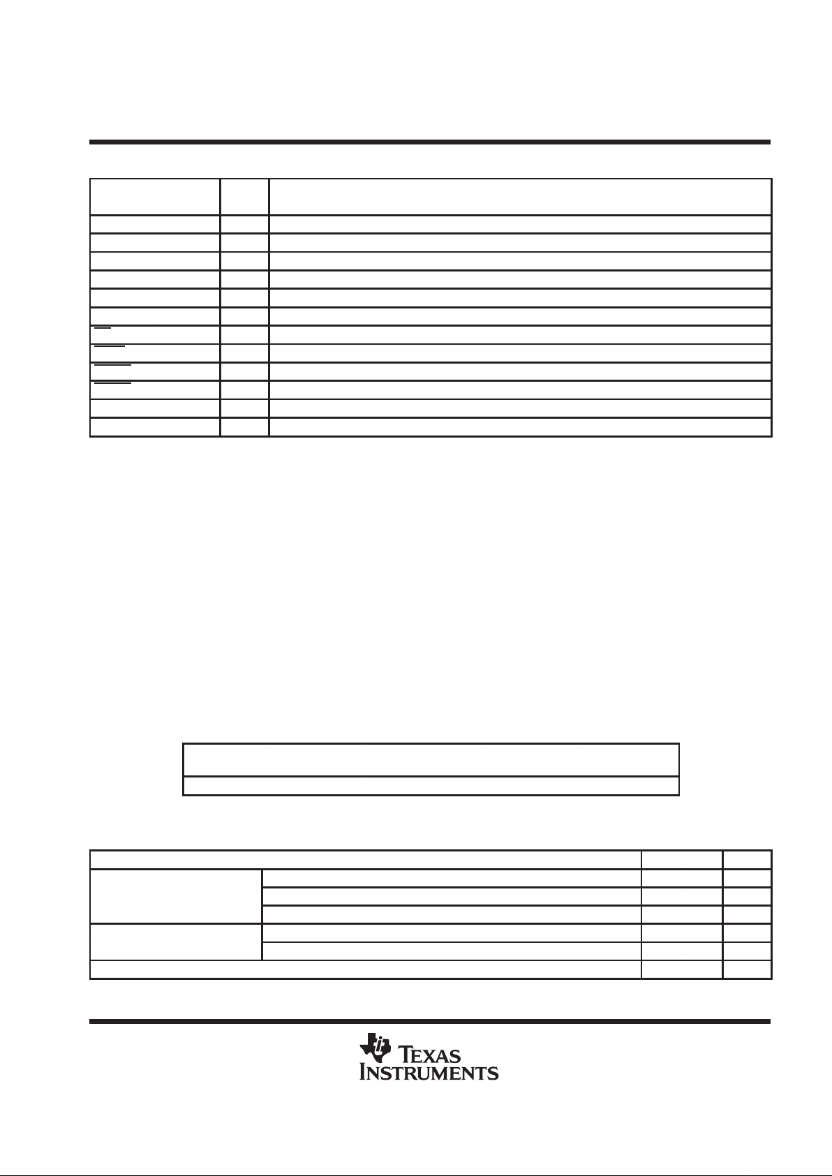
Terminal Functions
TERMINAL
NAME NO.
I/O
DESCRIPTION
3.3V 3, 4 I 3.3-V VCC input for card power and/or chip power if 5 V is not present
5V 5, 6 I 5-V VCC input for card power and/or chip power
VPPI 9 I Main VPP input, typically 12 V, allows 3.3 V–12 V.
VCC 11, 12, 13 O Switched output that delivers 0 V , 3.3-V, 5-V, or high impedance to card
VPP 10 O Switched output that delivers 0 V 3.3-V, 5-V, VPPI (12V), or high impedance to card
GND 7 Ground
OC 8 O Logic-level overcurrent reporting output that goes low when an overcurrent conditions exists
SHDN 16 I Logic input that shuts down the TPS2212 and sets all power outputs to high-impedance state
VCCD0 1 I Logic input that controls voltage of VCC (see control-logic table)
VCCD1 2 I Logic input that controls voltage of VCC (see control-logic table)
VPPD0 15 I Logic input that controls voltage of VPP (see control-logic table)
VPPD1 14 I Logic input that controls voltage of VPP (see control-logic table)
absolute maximum ratings over operating free-air temperature (unless otherwise noted)
†
Input voltage range for card power: V
I(5V)
–0.3 V to 7 V. . . . . . . . . . . . . . . . . . . . . . . . . . . . . . . . . . . . . . . . . . .
V
I(3.3V)
–0.3 V to 7 V. . . . . . . . . . . . . . . . . . . . . . . . . . . . . . . . . . . . . . . . .
V
I(VPPI)
–0.3 V to 14 V. . . . . . . . . . . . . . . . . . . . . . . . . . . . . . . . . . . . . . . .
Logic input voltage –0.3 V to 7 V. . . . . . . . . . . . . . . . . . . . . . . . . . . . . . . . . . . . . . . . . . . . . . . . . . . . . . . . . . . . . . . . .
Continuous total power dissipation See Dissipation Rating Table. . . . . . . . . . . . . . . . . . . . . . . . . . . . . . . . . . . . .
Output current (each card): I
O(VCC)
internally limited. . . . . . . . . . . . . . . . . . . . . . . . . . . . . . . . . . . . . . . . . . . . . .
I
O(VPP)
internally limited. . . . . . . . . . . . . . . . . . . . . . . . . . . . . . . . . . . . . . . . . . . . . .
Operating
virtual junction temperature range, T
J
–40°C to 150°C. . . . . . . . . . . . . . . . . . . . . . . . . . . . . . . . . . . . .
Operating free-air temperature range, T
A
–40°C to 85°C. . . . . . . . . . . . . . . . . . . . . . . . . . . . . . . . . . . . . . . . . . . .
Storage temperature range, T
stg
–55°C to 150°C. . . . . . . . . . . . . . . . . . . . . . . . . . . . . . . . . . . . . . . . . . . . . . . . . . .
Lead temperature 1.6 mm (1/16 inch) from case for 10 seconds 260°C. . . . . . . . . . . . . . . . . . . . . . . . . . . . . . .
†
Stresses beyond those listed under “absolute maximum ratings” may cause permanent damage to the device. These are stress ratings only, and
functional operation of the device at these or any other conditions beyond those indicated under “recommended operating conditions” is not
implied. Exposure to absolute-maximum-rated conditions for extended periods may affect device reliability.
DISSIPATION RATING TABLE
PACKAGE
TA ≤ 25°C
POWER RATING
DERATING FACTOR
ABOVE TA = 25°C
TA = 70°C
POWER RATING
TA = 85°C
POWER RATING
DB 775 mW 6.2 mW/°C 496 mW 403 mW
These devices are mounted on an FR4 board with no special thermal considerations.
recommended operating conditions
MIN MAX UNIT
V
I(5V)
0 5.25 V
Input voltage, V
I
V
I(3.3V)
0 5.25 V
V
I(VPPI)
0 13.5 V
p
I
O(VCC)
250 mA
Output Current
I
O(VPP)
150 mA
Operating virtual junction temperature, T
J
–40 125 °C
TPS2212
SINGLE-SLOT, PARALLEL INTERFACE POWER SWITCH
FOR LOW POWER PC CARD SLOTS
SLVS193 – APRIL 1999
4
POST OFFICE BOX 655303 • DALLAS, TEXAS 75265
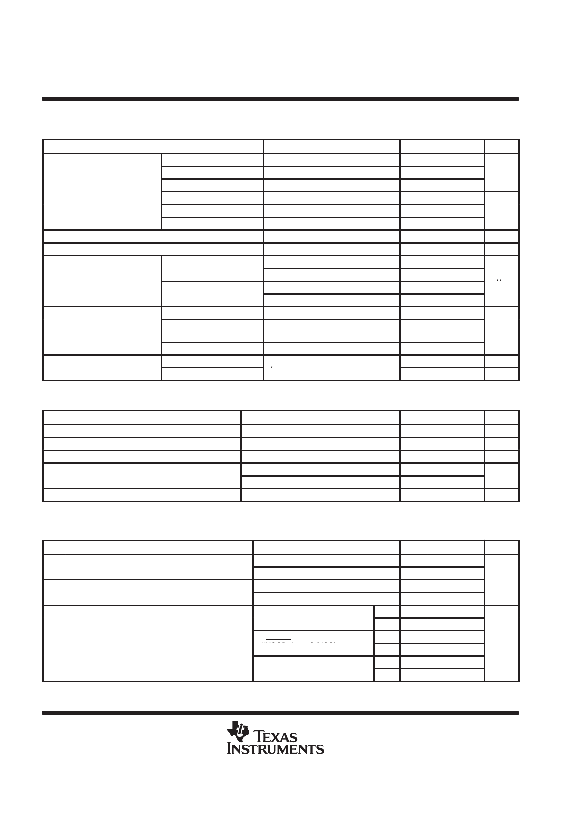
electrical characteristics, TA = –40°C to 85°C (unless otherwise noted)
power switch
PARAMETER
TEST CONDITIONS
†
MIN TYP MAX UNIT
5 V to VCC V
I(5V)
= 5 V 160 210
3.3 V to VCC V
I(5V)
= 5 V, V
I(3.3V)
= 3.3 V 160 210
mΩ
3.3 V to VCC V
I(5V)
= 0 V, V
I(3.3V)
= 3.3 V 160 210
Switch resistance
5 V to VPP TJ=25°C 6
3.3 V to VPP TJ=25°C 6
Ω
12 V to VPP TJ=25°C 1
V
O(VPP)
Clamp low voltage Ipp at 10 mA 0.8 V
V
O(VCC)
Clamp low voltage ICC at 10 mA 0.8 V
p
TA = 25°C 1 10
I
PP
high-impedance state
TA= 85°C 50
I
lkg
Leakage current
p
TA = 25°C 1 10
µ
A
I
CC
high-impedance state
TA=85°C 50
V
I(5V)
= 5 V V
O(VCC)
= 5 V, V
O(VPP)
= 12 V 40 150
I
I
Input current
V
I(5V)
= 0 V,
V
I(3.3V)
= 3.3 V
V
O(VCC)
= 3.3 V, V
O(VPP)
= 12 V 40 150
µA
Shutdown mode V
O(VCC)
= V
O(VPP)
= Hi-Z 1
Short-circuit
I
O(VCC)
TJ = 85°C, output powered into a
300 600 mA
I
OS
output-current limit
I
O(VPP)
J
short to GND
120 400 mA
†
Pulse-testing techniques maintain junction temperature close to ambient temperature; thermal effects must be taken into account separately.
logic section
PARAMETER
TEST CONDITIONS
†
MIN MAX UNIT
Logic input current 1 µA
Logic input high level 2 V
Logic input low level 0.8 V
p
V
I(5V)
= 5 V, IO = 1 mA V
I(5V)
– 0.4
Logic output high level
V
I(5V)
= 0 V, IO = 1 mA, V
I(3.3V)
= 3.3 V V
I(3.3V)
– 0.4
V
Logic output low level IO = 1 mA 0.4 V
†
Pulse-testing techniques maintain junction temperature close to ambient temperature; thermal effects must be taken into account separately.
switching characteristics
‡
PARAMETER
TEST CONDITIONS
§
MIN TYP MAX UNIT
p
V
O(VCC)
2.8
trRise times, output
V
O(VPP)
6.4
p
V
O(VCC)
4.5
ms
tfFall times, output
V
O(VPP)
12
t
on
6.8
V
I(VPPD0)
to
V
O(VPP)
t
off
18
p
t
on
4
tpdPropagation delay (see Figure1)
V
I(VCCD1)
to
V
O(VCC)
(3.
3V)
t
off
17
ms
t
on
6.6
V
I(VCCD0)
to
V
O(VCC)
(5V)
t
off
17
‡
Switching Characteristics are with CL = 150 µF.
§
Refer to Parameter Measurement Information
TPS2212
SINGLE-SLOT, PARALLEL INTERFACE POWER SWITCH
FOR LOW POWER PC CARD SLOTS
SLVS193 – APRIL 1999
5
POST OFFICE BOX 655303 • DALLAS, TEXAS 75265
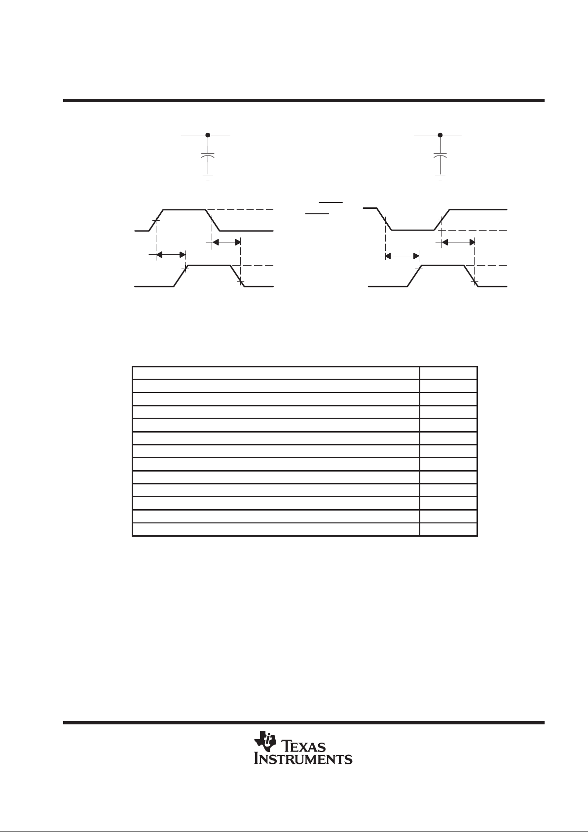
PARAMETER MEASUREMENT INFORMATION
t
off
t
off
LOAD CIRCUIT
C
L
t
on
VOLTAGE WAVEFORMS
V
I(VPPI)
GND
50%
90%
V
DD
GND
(V
I(VPPD1)
= 0 V)
V
O(VPP)
AVPP
LOAD CIRCUIT
C
L
AVCC
VOLTAGE WAVEFORMS
V
I(3.3V)
GND
50%
90%
10%
V
DD
GND
(V
I(VCCD0)
= VDD)
V
O(VCC)
10%
t
on
50%
50%
V
I(VPPD0)
V
I(VCCD1)
Figure 1. Test Circuits and Voltage Waveforms
Table of Timing Diagrams
FIGURE
VCC Propagation Delay and Rise Time With 1-µF Load, 3.3-V Switch 2
VCC Propagation Delay and Fall Time With 1-µF Load, 3.3-V Switch 3
VCC Propagation Delay and Rise Time With 150-µF Load, 3.3-V Switch 4
VCC Propagation Delay and Fall Time With 150-µF Load, 3.3-V Switch 5
VCC Propagation Delay and Rise Time With 1-µF Load, 5-V Switch 6
VCC Propagation Delay and Fall Time With 1-µF Load, 5-V Switch 7
VCC Propagation Delay and Rise Time With 150-µF Load, 5-V Switch 8
VCC Propagation Delay and Fall Time With 150-µF Load, 5-V Switch 9
VPP Propagation Delay and Rise Time With 1-µF Load, 12-V Switch 10
VPP Propagation Delay and Fall Time With 1-µF Load, 12-V Switch 11
VPP Propagation Delay and Rise Time With 150-µF Load, 12-V Switch 12
VPP Propagation Delay and Fall Time With 150-µF Load, 12-V Switch 13
TPS2212
SINGLE-SLOT, PARALLEL INTERFACE POWER SWITCH
FOR LOW POWER PC CARD SLOTS
SLVS193 – APRIL 1999
6
POST OFFICE BOX 655303 • DALLAS, TEXAS 75265
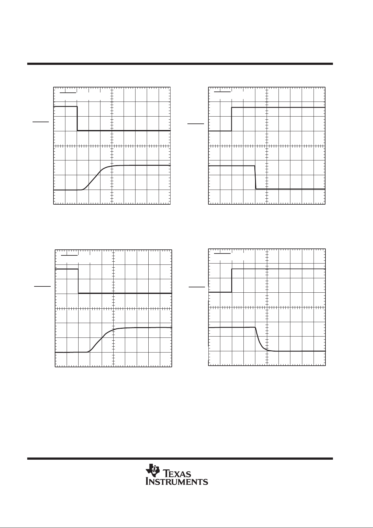
PARAMETER MEASUREMENT INFORMATION
Figure 2. VCC Propagation Delay and Rise Time
With 1-µF Load, 3.3-V Switch
032145768910
VCCD0 = 3.3 V
t – Time – ms
VCCD1
(2 V/div)
VCC
(2 V/div)
Figure 3. VCC Propagation Delay and Fall Time
With 1-µF Load, 3.3-V Switch
01510520253530 40 45 50
VCCD0 = 3.3 V
t – Time – ms
VCCD1
(2 V/div)
VCC
(2 V/div)
Figure 4. VCC Propagation Delay and Rise Time
With 150-µF Load, 3.3-V Switch
032145768910
VCCD0 = 3.3 V
t – Time – ms
VCCD1
(2 V/div)
VCC
(2 V/div)
Figure 5. VCC Propagation Delay and Fall Time
With 150-µF Load, 3.3-V Switch
01510520253530 40 45 50
VCCD0 = 3.3 V
t – Time – ms
VCCD1
(2 V/div)
VCC
(2 V/div)

TPS2212
SINGLE-SLOT, PARALLEL INTERFACE POWER SWITCH
FOR LOW POWER PC CARD SLOTS
SLVS193 – APRIL 1999
7
POST OFFICE BOX 655303 • DALLAS, TEXAS 75265
PARAMETER MEASUREMENT INFORMATION
Figure 6. VCC Propagation Delay and Rise Time
With 1-µF Load, 5-V Switch
0642 8 10 1412 16 18 20
VCCD1 = 5 V
t – Time – ms
VCCD0
(2 V/div)
VCC
(2 V/div)
Figure 7. VCC Propagation Delay and Fall Time
With 1-µF Load, 5-V Switch
01510520253530 40 45 50
VCCD1 = 5 V
t – Time – ms
VCC
(2 V/div)
VCCD0
(2 V/div)
Figure 8. VCC Propagation Delay and Rise Time
With 150-µF Load, 5-V Switch
0642 8 10 1412 16 18 20
VCCD1 = 5 V
t – Time – ms
VCCD0
(2 V/div)
VCC
(2 V/div)
Figure 9. VCC Propagation Delay and Fall Time
With 150-µF Load, 5-V Switch
01510520253530 40 45 50
VCCD1 = 5 V
t – Time – ms
VCCD0
(2 V/div)
VCC
(2 V/div)

TPS2212
SINGLE-SLOT, PARALLEL INTERFACE POWER SWITCH
FOR LOW POWER PC CARD SLOTS
SLVS193 – APRIL 1999
8
POST OFFICE BOX 655303 • DALLAS, TEXAS 75265
PARAMETER MEASUREMENT INFORMATION
Figure 10. VPP Propagation Delay and Rise Time
With 1-µF Load, 12-V Switch
0 0.60.40.2 0.8 1 1.41.2 1.6 1.8 2
VPPD1 = 0 V
t – Time – ms
VPPD0
(2 V/div)
VPP
(5 V/div)
Figure 11. VPP Propagation Delay and Fall Time
With 1-µF Load, 12-V Switch
032145768910
VPPD1 = 0 V
t – Time – ms
VPPD0
(2 V/div)
VPP
(5 V/div)
Figure 12. VPP Propagation Delay and Rise Time
With 150-µF Load, 12-V Switch
0642 8 10 1412 16 18 20
VPPD1 = 0 V
t – Time – ms
VPPD0
(2 V/div)
VPP
(5 V/div)
Figure 13. VPP Propagation Delay and Fall Time
With 150-µF Load, 12-V Switch
01510520253530 40 45 50
VPPD1 = 0 V
t – Time – ms
VPPD0
(2 V/div)
VPP
(5 V/div)

TPS2212
SINGLE-SLOT, PARALLEL INTERFACE POWER SWITCH
FOR LOW POWER PC CARD SLOTS
SLVS193 – APRIL 1999
9
POST OFFICE BOX 655303 • DALLAS, TEXAS 75265
TYPICAL CHARACTERISTICS
Table of Graphs
FIGURE
I
CC(5V)
Supply current vs Junction Temperature 14
I
CC(3.3V)
Supply current vs Junction Temperature 15
r
DS(on)
Static drain-source on-state resistance, 5-V VCC switch vs Junction Temperature 16
r
DS(on)
Static drain-source on-state resistance, 3.3-V VCC switch vs Junction Temperature 17
r
DS(on)
Static drain-source on-state resistance, 12-V VPP switch vs Junction Temperature 18
V
O(VCC)
Output voltage, 5-V VCC switch vs Output current 19
V
O(VCC)
Output voltage, 3.3-V VCC switch vs Output current 20
V
O(VPP)
Output voltage, 12-V VPP switch vs Output current 21
I
OS(VCC)
Short-circuit current, 5-V VCC switch vs Junction Temperature 22
I
OS(VCC)
Short-circuit current, 3.3-V VCC switch vs Junction Temperature 23
I
OS(VPP)
Short-circuit current, 12-V VPP switch vs Junction Temperature 24

TPS2212
SINGLE-SLOT, PARALLEL INTERFACE POWER SWITCH
FOR LOW POWER PC CARD SLOTS
SLVS193 – APRIL 1999
10
POST OFFICE BOX 655303 • DALLAS, TEXAS 75265
TYPICAL CHARACTERISTICS
Figure 14
39
37
35
–50 –25 0 25 50
– Supply Current –
41
43
SUPPLY CURRENT
vs
JUNCTION TEMPERATURE
45
75 100 125
TJ – Junction Temperature – °C
I
CC
Aµ
V
O(VCC)
= 5 V
V
O(VPP)
= 12 V
No Load
Figure 15
39
37
35
–50 –25 0 25 50
– Supply Current –
41
43
SUPPLY CURRENT
vs
JUNCTION TEMPERATURE
45
75 100 125
TJ – Junction Temperature – °C
I
CC
Aµ
V
O(VCC)
= 3.3 V
V
O(VPP)
= 12 V
No Load
Figure 16
140
120
100
80
–50 –25 0 25 50
– Static Drain-Source On-State Resistance – m
160
180
5–V VCC SWITCH
STATIC DRAIN-SOURCE ON-STATE RESISTANCE
vs
JUNCTION TEMPERATURE
200
75 100 125
TJ – Junction Temperature – °C
r
DS(on)
Ω
Figure 17
140
120
100
80
–50 –25 0 25 50
– Static Drain-Source On-State Resistance – m
160
180
3.3–V VCC SWITCH
STATIC DRAIN-SOURCE ON-STATE RESISTANCE
vs
JUNCTION TEMPERATURE
200
75 100 125
TJ – Junction Temperature – °C
r
DS(on)
Ω

TPS2212
SINGLE-SLOT, PARALLEL INTERFACE POWER SWITCH
FOR LOW POWER PC CARD SLOTS
SLVS193 – APRIL 1999
11
POST OFFICE BOX 655303 • DALLAS, TEXAS 75265
TYPICAL CHARACTERISTICS
Figure 18
1100
800
700
600
–50 –25 0 25 50
– Static Drain-Source On-State Resistance – m
1200
12-V VPP SWITCH
STATIC DRAIN-SOURCE ON-STATE RESISTANCE
vs
JUNCTION TEMPERATURE
75 100 125
900
TJ – Junction Temperature – °C
V
I(5V)
= 5 V
V
I(VPP)
= 12 V
r
DS(on)
Ω
1000
Figure 19
125°C
25°C
4.97
4.96
4.95
4.94
0 0.05 0.1 0.15
– Output Voltage – V
4.98
4.99
5-V VCC SWITCH
OUTPUT VOLTAGE
vs
OUTPUT CURRENT
5
0.2 0.25
I
O(VCC)
– Output Current – A
V
O(VCC)
–40°C
85°C
Figure 20
–40°C
125°C
85°C
25°C
3.27
3.26
3.25
0 0.05 0.1 0.15
– Output Voltage – V
3.28
3.29
3.3-V VCC SWITCH
OUTPUT VOLTAGE
vs
OUTPUT CURRENT
3.3
0.2 0.25
I
O(VCC)
– Output Current – A
V
O(VCC)
Figure 21
–40°C
125°C
25°C
85°C
11.96
11.94
11.86
11.84
0 0.03 0.06 0.09
11.98
12-V VPP SWITCH
OUTPUT VOLTAGE
vs
OUTPUT CURRENT
12
0.12
I
O(VPP)
– Output Current – A
11.92
11.9
11.88
– Output Voltage – V
V
O(VPP)

TPS2212
SINGLE-SLOT, PARALLEL INTERFACE POWER SWITCH
FOR LOW POWER PC CARD SLOTS
SLVS193 – APRIL 1999
12
POST OFFICE BOX 655303 • DALLAS, TEXAS 75265
TYPICAL CHARACTERISTICS
Figure 22
0.48
0.44
0.42
0.4
–50 –25 0 25 50 75 100
– Short-Circuit Output Current – A
0.5
0.52
5-V VCC SWITCH
SHORT-CIRCUIT CURRENT
vs
JUNCTION TEMPERATURE
0.54
125
0.46
I
OS(VCC)
TJ – Junction Temperature – °C
Figure 23
0.44
0.4
0.38
0.36
–50 –25 0 25 50 75 100
– Short-Circuit Output Current – A
0.46
0.48
3.3-V VCC SWITCH
SHORT-CIRCUIT CURRENT
vs
JUNCTION TEMPERATURE
0.5
125
0.42
I
OS(VCC)
TJ – Junction Temperature – °C
0.24
0.22
0.2
0.18
–50 –25 0 25 50
– Short-Circuit Output Current – A
12-V VPP SWITCH
SHORT-CIRCUIT CURRENT
vs
JUNCTION TEMPERATURE
0.28
75 100 125
0.26
I
OS(VPP)
TJ – Junction Temperature – °C
Figure 24

TPS2212
SINGLE-SLOT, PARALLEL INTERFACE POWER SWITCH
FOR LOW POWER PC CARD SLOTS
SLVS193 – APRIL 1999
13
POST OFFICE BOX 655303 • DALLAS, TEXAS 75265
APPLICATION INFORMATION
overview
PC Cards were initially introduced as a means to add EEPROM (flash memory) to portable computers with
limited on-board memory . The idea of add-in cards quickly took hold; modems, wireless LANs, GPS systems,
multimedia, and hard-disk versions were soon available. As the number of PC Card applications grew, the
engineering community quickly recognized the need for a standard to ensure compatibility across platforms.
To this end, the PCMCIA (Personal Computer Memory Card International Association) was established,
comprised of members from leading computer, software, PC Card, and semiconductor manufacturers. One key
goal was to realize the
plug and play
concept, i.e. cards and hosts from different vendors should be compatible.
PC Card power specification
System compatibility also means power compatibility . The most current set of specifications (PC Card Standard)
set forth by the PCMCIA committee states that power is to be transferred between the host and the card through
eight of the 68 terminals of the PC Card connectors. This power interface consists of two VCC, two VPP, and
four ground terminals. Multiple VCC and ground terminals minimize connector-terminal and line resistance. The
two VPP terminals were originally specified as separate signals, but are commonly tied together in the host to
form a single node to minimize voltage losses. Card primary power is supplied through the VCC terminals;
flash-memory programming and erase voltage is supplied through the VPP terminals.
designing for voltage regulation
The current PCMCIA specification for output voltage regulation of the 5-V output is 5% (250 mV). In a typical
PC power-system design, the power supply will have an output voltage regulation (V
PS(reg)
) of 2% (100 mV).
Also, a voltage drop from the power supply to the PC Card will result from resistive losses (V
PCB
) in the PCB
traces and the PCMCIA connector. A typical design would limit the total of these resistive losses to less than
1% (50 mV) of the output voltage. Therefore the allowable voltage drop (V
DS
) for the TPS2212 is the PCMCIA
voltage regulation less the power supply regulation and less the PCB and connector resistive drops:
V
DS
+
V
Oǒreg
Ǔ
–V
PSǒreg
Ǔ
–V
PCB
Typically, this would leave 100 mV for the allowable voltage drop across the TPS2212. The voltage drop is the
output current multiplied by the switch resistance of the TPS2212. Therefore, the maximum output current that
can be delivered to the PC Card in regulation is the allowable voltage drop across the TPS2212 divided by the
output switch resistance.
I
O
max
+
V
DS
r
DSǒon
Ǔ
The VCC outputs deliver 250 mA continuous at 5 V and 3.3 V within regulation over the operating temperature
range. Using the same equations, the PCMCIA specification for output voltage regulation of the 3.3 V output
is 300 mV . Using the voltage drop percentages for power supply regulation (2%) and PCB resistive loss (1%),
the allowable voltage drop for the 3.3 V switch is 200 mV . The 12-V outputs (VPP) of the TPS2212 can deliver
150 mA continuously .

TPS2212
SINGLE-SLOT, PARALLEL INTERFACE POWER SWITCH
FOR LOW POWER PC CARD SLOTS
SLVS193 – APRIL 1999
14
POST OFFICE BOX 655303 • DALLAS, TEXAS 75265
APPLICATION INFORMATION
overcurrent and overtemperature protection
PC Cards are inherently subject to damage from mishandling. Host systems require protection against
short-circuited cards that could lead to power supply or PCB trace damage. Even systems sufficiently robust
to withstand a short circuit would still undergo rapid battery discharge into the damaged PC Card, resulting in
a sudden loss of system power. Most hosts include fuses for protection. The reliability of fused systems is poor
and requires troubleshooting and repair, usually by the manufacturer, when fuses are blown.
The TPS2212 uses sense FET s to check for overcurrent conditions in each of the VCC and VPP outputs. Unlike
sense resistors or polyfuses, these FET s do not add to the series resistance of the switch; therefore voltage and
power losses are reduced. Overcurrent sensing is applied to each output separately. When an overcurrent
condition is detected, only the power output affected is limited; all other power outputs continue to function
normally. The OC
indicator, normally a logic high, is a logic low when an overcurrent condition is detected
providing for initiation of system diagnostics and/or sending a warning message to the user.
During power up, the TPS2212 controls the rise time of the VCC and VPP outputs and limits the current into
a faulty card or connector. If a short circuit is applied after power is established (e.g., hot insertion of a bad card),
current is initially limited only by the impedance between the short and the power supply . In extreme cases, as
much as 5 A to 10 A may flow into the short before the current limiting of the TPS2212 engages. If the VCC or
VPP outputs are driven below ground, the TPS2212 may latch nondestructively in an off state. Cycling power
will reestablish normal operation.
Overcurrent limiting for the VCC outputs is designed to activate if powered up into a short in the range of
300 mA to 600 mA, typically at about 450 mA. The VPP outputs limit from 120 mA to 400 mA, typically around
280 mA. The protection circuitry acts by linearly limiting the current passing through the switch rather than
initiating a full shutdown of the supply. Shutdown occurs only during thermal limiting.
Thermal limiting prevents destruction of the IC from overheating if the package power dissipation ratings are
exceeded. Thermal limiting disables power output until the device has cooled.
12-V supply not required
Most PC Card switches use the externally supplied 12 V to power gate drive and other chip functions, which
requires that power be present at all times. The TPS2212 offers considerable power savings by using an internal
charge pump to generate the required higher voltages from the 5-V input. Therefore, the external 12-V supply
can be disabled except when needed for flash-memory functions, thereby extending battery lifetime. Do not
ground the VPPI switch input when the VPPI input is not used. Additional power savings are realized by the
TPS2212 during a software shutdown in which quiescent current drops to a maximum of 1 µA.
3.3-V low-voltage mode
The TPS2212 will operate in a 3.3-V low-voltage mode when 3.3 V is the only available input voltage
(V
I(5V)
= 0). This allows host and PC Cards to be operated in low-power 3.3-volts-only modes such as sleep or
pager modes. Note that in these operation modes, the TPS2212 will derive its bias current from the 3.3-V input
pin and only 3.3 V can be delivered to the PC Card.

TPS2212
SINGLE-SLOT, PARALLEL INTERFACE POWER SWITCH
FOR LOW POWER PC CARD SLOTS
SLVS193 – APRIL 1999
15
POST OFFICE BOX 655303 • DALLAS, TEXAS 75265
APPLICATION INFORMATION
voltage transitioning requirement
PC Cards are migrating from 5 V to 3.3 V to minimize power consumption, optimize board space, and increase
logic speeds. The TPS2212 meets all combinations of power delivery as currently defined in the PCMCIA
standard. The latest protocol accommodates mixed 3.3-V/5-V systems by first powering the card with 5 V , then
polling it to determine its 3.3-V compatibility. The PCMCIA specification requires that the capacitors on 3.3-V
compatible cards be discharged to below 0.8 V before applying 3.3-V power. This functions as a power reset
and ensures that sensitive 3.3-V circuitry is not subjected to any residual 5-V charge. The TPS2212 offers a
selectable VCC and VPP ground state, in accordance with PCMCIA 3.3-V/5-V switching specifications.
output ground switches
PC Card specification requires that VCC be discharged within 100 ms. PC Card resistance can not be relied on
to provide a discharge path for voltages stored on PC Card capacitance because of possible high-impedance
isolation by power-management schemes.
power supply considerations
The TPS2212 has multiple pins for each of its 3.3-V and 5-V power inputs and for the switched VCC outputs.
Any individual pin can conduct the rated input or output current. Unless all pins are connected in parallel, the
series resistance is significantly higher than that specified, resulting in increased voltage drops and lost power.
It is recommended that all input and output power pins be paralleled for optimum operation.
To increase the noise immunity of the TPS2212, the power supply inputs should be bypassed with a 1-µF
electrolytic or tantalum capacitor paralleled by a 0.047-µF to 0.1-µF ceramic capacitor. It is strongly
recommended that the switched outputs be bypassed with a 0.1-µF, or larger, ceramic capacitor; doing so
improves the immunity of the TPS2212 to electrostatic discharge (ESD). Care should be taken to minimize the
inductance of PCB traces between the TPS2212 and the load. High switching currents can produce large
negative voltage transients, which forward biases substrate diodes, resulting in unpredictable performance.
Similarly, no pin should be taken below –0.3 V.
calculating junction temperature
The switch resistance, r
DS(on)
, is dependent on the junction temperature, TJ, of the die and the current through
the switch. To calculate T
J
, first find r
DS(on)
from Figures 16 through 18 using an initial temperature estimate
about 50°C above ambient. Then calculate the power dissipation for each switch, using the formula:
P
D
+
r
DSǒon
Ǔ
I
2
Next, sum the power dissipation and calculate the junction temperature:
T
J
+
ǒ
ȍ
PD
R
q
JA
Ǔ
)
TA,R
q
JA
+
108°CńW
Compare the calculated junction temperature with the initial temperature estimate. If the temperatures are not
within a few degrees of each other, recalculate using the calculated temperature as the initial estimate.

TPS2212
SINGLE-SLOT, PARALLEL INTERFACE POWER SWITCH
FOR LOW POWER PC CARD SLOTS
SLVS193 – APRIL 1999
16
POST OFFICE BOX 655303 • DALLAS, TEXAS 75265
APPLICATION INFORMATION
ESD protection
All TPS2212 inputs and outputs incorporate ESD-protection circuitry designed to withstand a 2-kV human-bodymodel discharge as defined in MIL-STD-883C, Method 3015. The VCC and VPP outputs can be exposed to potentially higher discharges from the external environment through the PC Card connector. Bypassing the outputs
with 0.1-µF capacitors protects the devices from discharges up to 10 kV.
SHDN
VPPD0
VPPD1
VCCD0
VCCD1
OC
Internal
Current Monitor
GND
Thermal
CS
CS
S4
S5
S6
13
12
11
10
17
51
18
52
V
CC1
V
CC2
V
pp1
V
pp2
Card B
S1
S2
S3
3
4
5
6
9
16
15
14
1
2
8
7
CPU
Controller
3.3 V
3.3 V
5 V
5 V
3.3 V to 12 V
VPPI
TPS2212
See Note A
NOTE A: MOSFET switch S6 has a back-gate diode from the source to the drain. Unused switch inputs should never be grounded.
Figure 25. Internal Switching Matrix, TPS2212 Control Logic

TPS2212
SINGLE-SLOT, PARALLEL INTERFACE POWER SWITCH
FOR LOW POWER PC CARD SLOTS
SLVS193 – APRIL 1999
17
POST OFFICE BOX 655303 • DALLAS, TEXAS 75265
APPLICATION INFORMATION
TPS2212 control logic
VPP
CONTROL SIGNALS INTERNAL SWITCH SETTINGS OUTPUT
SHDN VPPD0 VPPD1 S4 S5 S6 VPP
1 0 0 CLOSED OPEN OPEN 0 V
1 0 1 OPEN CLOSED OPEN VCC
†
1 1 0 OPEN OPEN CLOSED VPPI
1 1 1 OPEN OPEN OPEN Hi-Z
0 X X OPEN OPEN OPEN Hi-Z
†
Output depends on AVCC
VCC
CONTROL SIGNALS INTERNAL SWITCH SETTINGS OUTPUT
SHDN VCCD1 VCCD0 S1 S2 S3 VCC
1 0 0 CLOSED OPEN OPEN 0 V
1 0 1 OPEN CLOSED OPEN 3.3 V
1 1 0 OPEN OPEN CLOSED 5 V
1 1 1 CLOSED OPEN OPEN 0 V
0 X X OPEN OPEN OPEN Hi-Z

TPS2212
SINGLE-SLOT, PARALLEL INTERFACE POWER SWITCH
FOR LOW POWER PC CARD SLOTS
SLVS193 – APRIL 1999
18
POST OFFICE BOX 655303 • DALLAS, TEXAS 75265
APPLICATION INFORMATION
12-V flash memory supply
The TPS6734 is a fixed 12-V output boost converter capable of delivering 120 mA from inputs as low as
2.7 V . The device is pin-for-pin compatible with the MAX734 regulator and offers the following advantages: lower
supply current, wider operating input-voltage range, and higher output currents. As shown in Figure 26, the only
external components required are: an inductor, a Schottky rectifier, an output filter capacitor, an input filter
capacitor, and a small capacitor for loop compensation. The entire converter occupies less than 0.7 in
2
of PCB
space when implemented with surface-mount components. An enable input is provided to shut the converter
down and reduce the supply current to 3 µA when 12 V is not needed.
The TPS6734 is a 170-kHz current-mode PWM ( pulse-width modulation) controller with an n-channel MOSFET
power switch. Gate drive for the switch is derived from the 12-V output after start-up to minimize the die area
needed to realize the 0.7-Ω MOSFET and improve efficiency at input voltages below 5 V. Soft start is
accomplished with the addition of one small capacitor. A 1.22-V reference (pin 2) is brought out for external use.
For additional information, see the TPS6734 data sheet (SLVS127).
V
CC
FB
OUT
GND
EN
REF
SS
COMP
1
2
3
4
8
7
6
5
TPS6734
3.3 V or 5 V
ENABLE
(see Note A)
+
33 µF, 20 V
L1
18 µH
C5
D1
U1
C4 0.001 µF
+
C1
C2
0.01 µF
R1
10 kΩ
33 µF, 20 V
VCC
VCC
VCC
VPP
VCCD0
VCCD1
VPPD0
VPPD1
OC
SHDNGND
0.1 µF
0.1 µF
To CPU
TPS2212
12V
5V
5V
1 µF0.1 µF
5 V
3.3V
3.3V
1 µF0.1 µF
3.3 V
12 V
VPPI
NOTE A: The enable terminal can be tied to a generall purpose I/O terminal on the PCMCIA controller or tied high.
Figure 26. TPS2212 with TPS6734 12-V, 120-mA Supply

TPS2212
SINGLE-SLOT, PARALLEL INTERFACE POWER SWITCH
FOR LOW POWER PC CARD SLOTS
SLVS193 – APRIL 1999
19
POST OFFICE BOX 655303 • DALLAS, TEXAS 75265
MECHANICAL DATA
DB (R-PDSO-G**) PLASTIC SMALL-OUTLINE PACKAGE
4040065 /C 10/95
28 PIN SHOWN
Gage Plane
8,20
7,40
0,15 NOM
0,63
1,03
0,25
38
12,90
12,30
28
10,50
24
8,50
Seating Plane
9,907,90
30
10,50
9,90
0,38
5,60
5,00
15
0,22
14
A
28
1
2016
6,50
6,50
14
0,05 MIN
5,905,90
DIM
A MAX
A MIN
PINS **
2,00 MAX
6,90
7,50
0,65
M
0,15
0°–8°
0,10
3,30
8
2,70
NOTES: A. All linear dimensions are in millimeters.
B. This drawing is subject to change without notice.
C. Body dimensions do not include mold flash or protrusion not to exceed 0,15.
D. Falls within JEDEC MO-150

IMPORTANT NOTICE
T exas Instruments and its subsidiaries (TI) reserve the right to make changes to their products or to discontinue
any product or service without notice, and advise customers to obtain the latest version of relevant information
to verify, before placing orders, that information being relied on is current and complete. All products are sold
subject to the terms and conditions of sale supplied at the time of order acknowledgement, including those
pertaining to warranty, patent infringement, and limitation of liability.
TI warrants performance of its semiconductor products to the specifications applicable at the time of sale in
accordance with TI’s standard warranty. Testing and other quality control techniques are utilized to the extent
TI deems necessary to support this warranty. Specific testing of all parameters of each device is not necessarily
performed, except those mandated by government requirements.
CERT AIN APPLICATIONS USING SEMICONDUCTOR PRODUCTS MA Y INVOLVE POTENTIAL RISKS OF
DEATH, PERSONAL INJURY, OR SEVERE PROPERTY OR ENVIRONMENTAL DAMAGE (“CRITICAL
APPLICATIONS”). TI SEMICONDUCTOR PRODUCTS ARE NOT DESIGNED, AUTHORIZED, OR
WARRANTED TO BE SUITABLE FOR USE IN LIFE-SUPPORT DEVICES OR SYSTEMS OR OTHER
CRITICAL APPLICATIONS. INCLUSION OF TI PRODUCTS IN SUCH APPLICA TIONS IS UNDERST OOD TO
BE FULLY AT THE CUSTOMER’S RISK.
In order to minimize risks associated with the customer’s applications, adequate design and operating
safeguards must be provided by the customer to minimize inherent or procedural hazards.
TI assumes no liability for applications assistance or customer product design. TI does not warrant or represent
that any license, either express or implied, is granted under any patent right, copyright, mask work right, or other
intellectual property right of TI covering or relating to any combination, machine, or process in which such
semiconductor products or services might be or are used. TI’s publication of information regarding any third
party’s products or services does not constitute TI’s approval, warranty or endorsement thereof.
Copyright 1999, Texas Instruments Incorporated
 Loading...